EP1995844B1 - A method for detecting connection of remote power supply and a line powering method and system - Google Patents
A method for detecting connection of remote power supply and a line powering method and system Download PDFInfo
- Publication number
- EP1995844B1 EP1995844B1 EP07711034A EP07711034A EP1995844B1 EP 1995844 B1 EP1995844 B1 EP 1995844B1 EP 07711034 A EP07711034 A EP 07711034A EP 07711034 A EP07711034 A EP 07711034A EP 1995844 B1 EP1995844 B1 EP 1995844B1
- Authority
- EP
- European Patent Office
- Prior art keywords
- powered device
- capacitor
- voltage
- timing
- charge
- Prior art date
- Legal status (The legal status is an assumption and is not a legal conclusion. Google has not performed a legal analysis and makes no representation as to the accuracy of the status listed.)
- Active
Links
Images




Classifications
-
- H—ELECTRICITY
- H04—ELECTRIC COMMUNICATION TECHNIQUE
- H04M—TELEPHONIC COMMUNICATION
- H04M19/00—Current supply arrangements for telephone systems
- H04M19/001—Current supply source at the exchanger providing current to substations
-
- H—ELECTRICITY
- H04—ELECTRIC COMMUNICATION TECHNIQUE
- H04L—TRANSMISSION OF DIGITAL INFORMATION, e.g. TELEGRAPHIC COMMUNICATION
- H04L12/00—Data switching networks
- H04L12/02—Details
- H04L12/10—Current supply arrangements
Definitions
- the present invention relates to the field of electronics and communication technology; and in particular to a method and system for remote power supplying.
- the carriers keep on developing new services for end users by using the already installed subscriber line networks, or providing new services by laying new subscriber networks.
- a general way is to move the broadband and narrowband products closer to the subscriber, in which twisted pairs or coaxial cables are used as up links, and more subscribers and services can be configured on the subscriber side.
- the powering becomes a practical problem difficult to be solved, due to the complicated subscriber environment and inconvenience of supplying power in most cases.
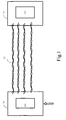
- Fig. 1 shows the operating principle of a typical remote power supply system using this method.
- the remote power supply system includes a central office apparatus 10 and a remote apparatus 11; a power supply module in the central office apparatus 101 supplies a feeding high voltage to a powered device in the remote apparatus 111 via the subscriber line 12, such as twisted pairs or coaxial cables.
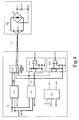
- Fig. 2 is a detailed circuit diagram of the above remote power supply system.
- a voltage conversion unit 201 in the central office power source 21 includes, but is not limited to, a transformer, a diode and a MOS transistor, boosts an input 48V DC voltage, and supplies the boosted DC high voltage to the powered device via a pair or several pairs of subscriber lines.
- a voltage conversion unit 202 reduces the DC high voltage fed through the subscriber lines, and the reduced DC voltage is used as a power for the remote communication device (now shown).
- the communication device may be an xDSL device, etc.
- the boosted voltage generated by the voltage conversion unit at the central office is normally a dangerous voltage higher than 60V, and is transferred to the powered device through the existing low voltage communication network. Since it cannot be determined whether the powered device is reliably connected (hereafter referred to as "ready"), when the high voltage is output and the powered device is not reliably connected, the possibility that the maintenance and operating staff may get shocked will increase when they touch the wire.
- FIG. 3 Another remote power supply system is shown in Fig. 3 , which includes a central office power source 31, a powered device 32 and at least four pairs of subscriber lines 33.
- the central office power source 31 and the powered device 32 can communicate via the communication channels A1, A2, B1 and B2, and the signal processing for the central office power source 31 and the powered device 32 are performed via the internal control circuit 311, 321 and power conversion circuit 312, 322 at the central office power source and the powered device, respectively.
- the communication channels A1, A2, B1 and B2 also carry the remote power transmission.
- the communication channels A1 and A2 couple to signal input terminal 1, the communication channel B1 couples to signal transmitting terminal 2, and the communication channel B2 couples to signal receiving terminal 3.
- the power conversion circuit 312 of the central office power source 31 is connected to a power input terminal 4, and the power conversion circuit 322 of the powered device 32 is connected to a power output terminal 5.
- the purpose of the above communication is to set up power monitoring for the central office and powered device, and the detail procedure is as follows.
- the central office power source controls the power conversion circuit to output a DC low voltage usually lower than 60V, which is used as the power needed for operating the control circuit at the powered device;
- a predefined protocol it may be a general protocol such as ADSL protocol or a customized protocol
- control circuit at the central office controls the power conversion circuit at the central office to output the high voltage, so as to supply electric power to the powered device.
- the above solution makes it possible for the communication signals and the electric power to share the channels without interfering each other, and implements coupling the signal to the electric power. It can effectively prevent the maintenance and operating staff from getting shocked when touching the wire, by determining whether the powered device is ready before supplying the DC high voltage to the powered device.
- Communication circuits and the predefined communication protocol must be designed to implement the powered device communicating with the central office, which would significantly increase the design complexity in terms of both hardware and software.
- US 3 870 822 A discloses a power supply at a point remote from a control power source by way of a telephone line.
- the remote power supply is generally derived from a rechargeable battery.
- the battery charging current is only supplied to the line when it is in an "idle" state. This idle state is sensed at the power transmitter and receiver and the charging source and chargeable source are then coupled to the line.
- GB 2 223 379A discloses bell capacitance circuit to perform the remote measurement of the bell capacitance in the line conductors at a telephone receiver.
- the circuit includes a capacitor, means for charging said capacitor, line conductor of the receiver and high impedance monitoring means.
- Embodiments of the present invention provide a method for detecting connection of a powered device, and a remote power supplying system.
- An embodiment of the present invention provides a central office power source, connected with a powered device via subscriber lines, the central office power source has a power supply module, a timing and control circuit and comparator circuits.
- the comparator circuits, the subscriber lines and a characteristic capacitor of the powered device form a resistor-capacitor charge/discharge loop
- the comparator circuits are adapted to detect a voltage input therein during the charge/discharge of the characteristic capacitor Ct, and output a corresponding level signal to the timing and control circuit;
- the timing and control circuit is adapted to control the charge/discharge of the charge/discharge loop according to the level signal, and determines whether the powered device is ready according to a discharge time of the charge/discharge loop;
- the power supply module connected to the timing and control circuit is configured to supply a voltage higher than 60V to the powered device when the powered device is ready.
- An embodiment of the present invention provides a remote power supplying method, including the steps of:
- An embodiment of the present invention provides a method for detecting a powered device, including the steps of:
- the time difference produced in the charge/discharge procedure is used as a basis of determination for logically determining whether the powered device is ready.
- the low voltage test procedure it is checked whether the powered device is ready by using the resistor-capacitor charge/discharge, and the implementation is easy to be realized and of low cost and high reliability.
- the remote voltage is output only when the powered device is reliably connected.
- the technical solutions can effectively prevent electric shock from happening and guarantee the safety of the operating and maintenance staff.
- Fig. 1 shows the operating principle of remote power supply system according to a prior art
- Fig. 2 shows a detailed circuit of the remote power supply system shown in Fig. 1 ;
- Fig. 3 shows a detailed circuit of remote power supply system according to another prior art
- Fig. 4 is a structural diagram of a remote power supply system according to a first embodiment of the present invention.
- Fig. 5 is a structural diagram of a remote power supply system according to a second embodiment of the present invention.
- Fig. 6 is a structural diagram of a remote power supply system according to a third embodiment of the present invention.
- Fig. 7 is a structural diagram of a remote power supply system according to a fourth embodiment of the present invention.
- Fig. 4 shows a schematic diagram of a remote power supply system according to an embodiment of the present invention.
- the central office power source 41 of the remote power supply system includes a power conversion circuit 411, a switch circuit 412, a timing and control circuit 413 and a comparator circuit 414.
- the powered device 42 includes a characteristic capacitor Ct 421.
- the central office and the powered device are connected via subscriber lines 43, which may be equivalent to a resistor Rp and a distributed capacitor Cp.
- the powered device is further provided with a diode circuit (or a bridge rectifier) Dz 422.
- the power conversion circuit In the central office power source, the power conversion circuit generates a test low voltage Vt and a feeding high voltage Vh, where the test low voltage V1 is usually lower than 60V and the feeding high voltage Vh is usually a DC voltage higher than 60V.
- the system also includes one power conversion circuit, which outputs the test low voltage Vt and the feeding high voltage Vh by correspondingly converting the input voltage. It should be noted that only one of the test low voltage Vt and the feeding high voltage Vh is supplied to the powered device via the subscriber line at a time.
- the test low voltage Vt output from the power conversion circuit is fed to a first comparator circuit 1 and a second comparator circuit2, respectively.
- the first comparator circuit 1 and the second comparator circuit 2 are adapted to detect a voltage input therein during the charge/discharge of the characteristic capacitor Ct, and output a corresponding voltage according to a change in the voltage input to the characteristic capacitor Ct.
- the first comparator circuit 1 includes a voltage divider network composed of resistors R1 and R2, a reference power source and a comparator.
- the non-inverse input of the comparator is a terminal voltage of the resistor R2; the inverse input of the comparator is an internal reference voltage Vs; and the output voltage Vc1 of the comparator is output to the timing and control circuit, as a first input voltage.
- the second comparator circuit 2 includes a voltage divider network composed of resistors R3 and R4 and a comparator.
- the non-inverse input of the comparator is a terminal voltage of resistor R4; the inverse input of the comparator is an internal reference voltage Vs; and the output voltage Vc2 of the comparator is output to the timing and control circuit, as a second input voltage.
- resistors R1, R2, R3 and R4 form voltage divider networks for detecting the test low voltage Vt; and the test low voltage Vt is compared with the internal reference voltage Vs so as to output a corresponding high/low level.
- Vt1 and Vt2 are not limited to the above examples.
- the timing and control circuit generates a switch signal QH (from high to low, or from low to high) according to the received output voltage Vc1, Vc2 output from the first comparator circuit 1 and the second comparator circuit 2, and further controls the switch circuit to switch between the test low voltage and the feeding high voltage.
- the timing and control circuit also generates signals KC1 or KC2 for controlling the power conversion circuit, according to the output voltage Vc1, Vc2 of the first comparator circuit 1 and the second comparator circuit 2, and controls the output of the power conversion circuit to turn on/off.
- the subscriber lines are connected to both terminals of the remote characteristic capacitor Ct; and the test low voltage Vt provide by the central office charges the remote characteristic capacitor Ct, so that the detect.
- the capacitance of the characteristic capacitor Ct is sufficient large with respect to the distributed capacitance Cp of the subscriber lines, so that the distributed capacitance Cp of the subscriber lines is negligible when identifying the characteristic capacitor Ct during the timing procedure.
- the diode circuit (or a bridge rectifier) Dz in the powered device is used to isolate the characteristic capacitor Ct from the capacitor Cin, so that the identifying of the characteristic capacitor Ct is speeded up during the timing procedure.
- the voltage divider networks composed of R1, R2 as well as R3 and R4 together with the equivalent resistor Rp and the distributed capacitor Cp of the subscriber lines and the remote characteristic capacitor Ct form a resistor-capacitor charge/discharge loop, thereby a certain delay occurs during the charge/discharge procedure, and the time and control circuit uses the delay to perform control and timing.
- the resistance of the voltage divider network should be sufficient large with respect to the equivalent resistance Rp of the subscriber lines, so that the affection of the resistance Rp of the subscriber lines can be ignored during the timing procedure.
- the timing and control circuit obtains the distributed capacitance of the subscriber lines according to the above delay, i.e., the time period between starting and finishing the discharge timing; and compares the distributed capacitance of the subscriber lines with the characteristic capacitor Ct (e.g. 1 ⁇ F); if the obtained distributed capacitance satisfies a predetermined condition (e.g. larger than 1 ⁇ F), then the powered device is considered as being connected normally (ready).
- the characteristic capacitor Ct e.g. 1 ⁇ F
- the remote power supplying method provided in an embodiment of the present invention includes a low voltage test procedure and a remote powering procedure; the low voltage test procedure is the procedure for determining the powered device.
- the timing and control circuit first controls the power conversion circuit to output the test low voltage Vt, which is fed to the first comparator circuit and the second comparator circuit respectively.
- the test low voltage Vt is also supplied to the powered device via the subscriber lines, as the terminal voltage of the characteristic capacitor Ct.
- the test low voltage Vt charges the subscriber line capacitor Cp and the characteristic capacitor Ct via the voltage divider resistors of the comparator circuit and the subscriber line resistor Rp.
- the timing and control circuit controls the power conversion circuit to disconnect the output, and the subscriber line capacitor Cp and characteristic capacitor Ct of the powered device discharge through the voltage divider resistors of the comparator circuit and the subscriber line resistor Rp.
- the timing and control circuit stops timing, computes the total capacitance of the lines (the whole charge/discharge loop) according to Eq. (1), based on the delay between starting timing and stopping timing. Then it is determined whether the powered device is ready according to the computed total capacitance of the lines.
- U c U 0 ⁇ e - t / ⁇
- ⁇ RC
- R is the equivalent resistance of the charge/ discharge loop
- C is the equivalent capacitance of the charge/discharge loop
- U c is an end voltage of the equivalent capacitor
- U 0 is the initial voltage of the equivalent capacitor.
- the total capacitance of the lines (the whole charge/discharge loop) is larger than the characteristic capacitance Ct, it can be determined that the powered device is reliably connected, and that the powered device is ready; otherwise the powered device is not ready; and the low voltage test procedure is repeated.
- the resistor-capacitor charge/discharge principle is used to detect whether the powered device is ready, which is easy to be implemented and low cost and high reliability.
- the timing and control circuit switches the switch in the switching circuit to the output terminal of the power conversion circuit that outputs the feeding high voltage by using the QH signal. Meanwhile, the timing and control circuit controls the power conversion circuit to output the feeding high voltage by using the KCl signal, and supply the high voltage power to the powered device via the subscriber lines.
- Fig. 5 shows a schematic diagram of a remote power supply system according to a second embodiment of the present invention.
- the second embodiment is substantially the same as the first embodiment, and the difference between the two embodiments lies in that the powered device further includes a signal transformer 523 and the characteristic capacitor Ct is arranged at the center tap of the signal transformer.
- Fig. 6 shows a schematic diagram of a remote power supply system according to a third embodiment of the present invention.
- the third embodiment is substantially the same as the first embodiment, and the difference between the two embodiments lies in that in third embodiment, the capacitor Cin 621 for storing electric energy and filtering within the powered device is directly used as the characteristic capacitor to replace the characteristic capacitor Ct and the diode circuit (or a bridge rectifier) Dz.
- the remote power supply system of the third embodiment can reduce design complexity and the cost, on the basis of realizing safe powering.
- Fig. 7 shows a schematic diagram of a remote power supply system according to a fourth embodiment of the present invention.
- the fourth embodiment is substantially the same as the third embodiment, and the difference between them lies in that the powered device further includes a signal transformer, and the capacitor Cin as the characteristic capacitor Ct is arranged at the center tap of the signal transformer.
- the remote power system of the fourth embodiment can further reduce design complexity and the cost, on the basis of realizing safe powering.
- the two resistor networks in the comparator circuits are first connected in series and then connected in parallel, which corresponds to a resistor and can be equivalent to a loop.
- another charge/discharge resistor network may be further added when necessary, for example, when the resistors in the comparator circuit of the above charge/discharge loop are connected, in parallel, with one or more resistors having resistances much smaller than that of any of the voltage dividing resistors, as a result, the resistance of the comparator circuit can be ignored when determining whether the powered device is ready.
- one or more comparator circuits may also be used to provide the output level, as the basis of controlling charge/discharge by the timing and control circuit.
- the high level output by the comparator circuit is used to trigger the timing and control circuit to start the discharge timing
- the low level output by the comparator circuit is used to trigger the timing and control circuit to stop the timing
- a low level may also be used to trigger timing start and the high level may be used to trigger timing stop.
- the non-inverse input of the comparator may be not limited to be the terminal voltage of the voltage dividing resistor, and the inverse input of the comparator may be not limited to be the voltage of the reference power source.
- the same effect can be achieved by taking the voltage of the reference power source as the non-inverse input and taking the terminal voltage of the voltage dividing resistor as the inverse input of the comparator, if only the trigger level for the timing and control circuit is changed to be high or low.
Landscapes
- Engineering & Computer Science (AREA)
- Signal Processing (AREA)
- Computer Networks & Wireless Communication (AREA)
- Direct Current Feeding And Distribution (AREA)
- Cable Transmission Systems, Equalization Of Radio And Reduction Of Echo (AREA)
- Selective Calling Equipment (AREA)
- Remote Monitoring And Control Of Power-Distribution Networks (AREA)
- Devices For Supply Of Signal Current (AREA)
- Circuits Of Receivers In General (AREA)
Abstract
Description
- The present invention claims a priority to Chinese Patent Application No.
200610058189.5 - The present invention relates to the field of electronics and communication technology; and in particular to a method and system for remote power supplying.
- With the continuous increasing of communication service requirement, the carriers keep on developing new services for end users by using the already installed subscriber line networks, or providing new services by laying new subscriber networks. A general way is to move the broadband and narrowband products closer to the subscriber, in which twisted pairs or coaxial cables are used as up links, and more subscribers and services can be configured on the subscriber side. However, when moving devices to the subscriber side, the powering becomes a practical problem difficult to be solved, due to the complicated subscriber environment and inconvenience of supplying power in most cases.
- Under this circumstance, the carriers use a method for supplying power from the office end (i.e., Line Powering), which is an essential technical solution for expanding services and subscribers.
Fig. 1 shows the operating principle of a typical remote power supply system using this method. The remote power supply system includes acentral office apparatus 10 and aremote apparatus 11; a power supply module in thecentral office apparatus 101 supplies a feeding high voltage to a powered device in theremote apparatus 111 via thesubscriber line 12, such as twisted pairs or coaxial cables. -
Fig. 2 is a detailed circuit diagram of the above remote power supply system. As shown inFig. 2 , avoltage conversion unit 201 in the centraloffice power source 21 includes, but is not limited to, a transformer, a diode and a MOS transistor, boosts an input 48V DC voltage, and supplies the boosted DC high voltage to the powered device via a pair or several pairs of subscriber lines. At theremote apparatus 22, avoltage conversion unit 202 reduces the DC high voltage fed through the subscriber lines, and the reduced DC voltage is used as a power for the remote communication device (now shown). Here the communication device may be an xDSL device, etc. - It has been found that the above prior art has at least the following problem.
- In the remote power supply system, the boosted voltage generated by the voltage conversion unit at the central office is normally a dangerous voltage higher than 60V, and is transferred to the powered device through the existing low voltage communication network. Since it cannot be determined whether the powered device is reliably connected (hereafter referred to as "ready"), when the high voltage is output and the powered device is not reliably connected, the possibility that the maintenance and operating staff may get shocked will increase when they touch the wire.
- Another remote power supply system is shown in
Fig. 3 , which includes a centraloffice power source 31, a powereddevice 32 and at least four pairs of subscriber lines 33. Where, the centraloffice power source 31 and the powereddevice 32 can communicate via the communication channels A1, A2, B1 and B2, and the signal processing for the centraloffice power source 31 and the powereddevice 32 are performed via theinternal control circuit power conversion circuit signal input terminal 1, the communication channel B1 couples to signal transmittingterminal 2, and the communication channel B2 couples to signal receivingterminal 3. Thepower conversion circuit 312 of the centraloffice power source 31 is connected to apower input terminal 4, and thepower conversion circuit 322 of the powereddevice 32 is connected to apower output terminal 5. - The purpose of the above communication is to set up power monitoring for the central office and powered device, and the detail procedure is as follows.
- First, the central office power source controls the power conversion circuit to output a DC low voltage usually lower than 60V, which is used as the power needed for operating the control circuit at the powered device;
- After the central office and the powered device establishing the communication according to a predefined protocol (it may be a general protocol such as ADSL protocol or a customized protocol), it is determined whether the powered device is ready.
- When the powered device is ready, the control circuit at the central office controls the power conversion circuit at the central office to output the high voltage, so as to supply electric power to the powered device.
- The above solution makes it possible for the communication signals and the electric power to share the channels without interfering each other, and implements coupling the signal to the electric power. It can effectively prevent the maintenance and operating staff from getting shocked when touching the wire, by determining whether the powered device is ready before supplying the DC high voltage to the powered device.
- However, it was found that the above prior art has the following problem.
- Communication circuits and the predefined communication protocol must be designed to implement the powered device communicating with the central office, which would significantly increase the design complexity in terms of both hardware and software.
- Because of the high design complexity, a problem occurring in any part of the hardware and software may lead to communication abnormality, and may result in that the powered device cannot start up, and as a result, the reliability of service is degraded.
-
US 3 870 822 A discloses a power supply at a point remote from a control power source by way of a telephone line. The remote power supply is generally derived from a rechargeable battery. The battery charging current is only supplied to the line when it is in an "idle" state. This idle state is sensed at the power transmitter and receiver and the charging source and chargeable source are then coupled to the line.GB 2 223 379A - Embodiments of the present invention provide a method for detecting connection of a powered device, and a remote power supplying system.
- An embodiment of the present invention provides a central office power source, connected with a powered device via subscriber lines, the central office power source has a power supply module, a timing and control circuit and comparator circuits.
- The comparator circuits, the subscriber lines and a characteristic capacitor of the powered device form a resistor-capacitor charge/discharge loop;
- The comparator circuits are adapted to detect a voltage input therein during the charge/discharge of the characteristic capacitor Ct, and output a corresponding level signal to the timing and control circuit;
- The timing and control circuit is adapted to control the charge/discharge of the charge/discharge loop according to the level signal, and determines whether the powered device is ready according to a discharge time of the charge/discharge loop; and
- The power supply module connected to the timing and control circuit, is configured to supply a voltage higher than 60V to the powered device when the powered device is ready.
- An embodiment of the present invention provides a remote power supplying method, including the steps of:
- feeding a test low voltage to a comparator circuit, providing the test low voltage to a characteristic capacitor via subscriber lines, and charging a charge/discharge loop formed of the subscriber lines and the characteristic capacitor;
- under the control of a timing and control circuit, stopping the feeding test low voltage when an output level of the comparator circuit is a first level; starting timing of the timing and control circuit, and controlling the charge/discharge loop to discharge;
- stopping the timing of the timing and control circuit when the output level of the comparator circuit is a second level, and determining whether the powered device is ready according to a discharge time of the charge/discharge loop; and
- supplying a remote feeding high voltage to the powered device via the subscriber lines when determining that the powered device is ready.
- An embodiment of the present invention provides a method for detecting a powered device, including the steps of:
- feeding a test voltage to a comparator circuit and providing the test voltage to a characteristic capacitor of the powered device via subscriber lines;
- stopping the feeding the test voltage under the control of a timing and control circuit, when an output level of the comparator circuit is a first level, so that a charge/discharge loop formed of the subscriber lines and the characteristic capacitor discharges, and starting the timing of the timing and control circuit; and
- stopping the timing of the timing and control circuit when the charge/discharge loop discharges to make the output level of the comparator circuit to be a second level, obtaining a discharge time, and determining whether the powered device is ready according to the discharge time.
- In the technical solutions of the embodiments of the present invention, by use of the resistor-capacitor charge/discharge principle, the time difference produced in the charge/discharge procedure is used as a basis of determination for logically determining whether the powered device is ready. During the low voltage test procedure, it is checked whether the powered device is ready by using the resistor-capacitor charge/discharge, and the implementation is easy to be realized and of low cost and high reliability.
- Since it is tested that the powered device is ready during the low voltage test procedure, the remote voltage is output only when the powered device is reliably connected. As a result, the technical solutions can effectively prevent electric shock from happening and guarantee the safety of the operating and maintenance staff.
-
Fig. 1 shows the operating principle of remote power supply system according to a prior art; -
Fig. 2 shows a detailed circuit of the remote power supply system shown inFig. 1 ; -
Fig. 3 shows a detailed circuit of remote power supply system according to another prior art; -
Fig. 4 is a structural diagram of a remote power supply system according to a first embodiment of the present invention; -
Fig. 5 is a structural diagram of a remote power supply system according to a second embodiment of the present invention; -
Fig. 6 is a structural diagram of a remote power supply system according to a third embodiment of the present invention; and -
Fig. 7 is a structural diagram of a remote power supply system according to a fourth embodiment of the present invention; - A central office power source, the method for determining a powered device according to the present invention will be explained in the following with reference to the accompany drawing and embodiments.
-
Fig. 4 shows a schematic diagram of a remote power supply system according to an embodiment of the present invention. The centraloffice power source 41 of the remote power supply system includes apower conversion circuit 411, aswitch circuit 412, a timing andcontrol circuit 413 and acomparator circuit 414. Thepowered device 42 includes acharacteristic capacitor Ct 421. The central office and the powered device are connected viasubscriber lines 43, which may be equivalent to a resistor Rp and a distributed capacitor Cp. The powered device is further provided with a diode circuit (or a bridge rectifier)Dz 422. - In the central office power source, the power conversion circuit generates a test low voltage Vt and a feeding high voltage Vh, where the test low voltage V1 is usually lower than 60V and the feeding high voltage Vh is usually a DC voltage higher than 60V. In
Fig. 4 , two power conversion circuits are used to provide the test low voltage Vt and the feeding high voltage Vh respectively; and one of the test low voltage Vt and remote feeding high voltage Vh is supplied to the powered device via the subscriber line, by the switching of the switch circuit. However, in an embodiment of the present invention, the system also includes one power conversion circuit, which outputs the test low voltage Vt and the feeding high voltage Vh by correspondingly converting the input voltage. It should be noted that only one of the test low voltage Vt and the feeding high voltage Vh is supplied to the powered device via the subscriber line at a time. - The test low voltage Vt output from the power conversion circuit is fed to a
first comparator circuit 1 and a second comparator circuit2, respectively. Thefirst comparator circuit 1 and thesecond comparator circuit 2 are adapted to detect a voltage input therein during the charge/discharge of the characteristic capacitor Ct, and output a corresponding voltage according to a change in the voltage input to the characteristic capacitor Ct. Thefirst comparator circuit 1 includes a voltage divider network composed of resistors R1 and R2, a reference power source and a comparator. The non-inverse input of the comparator is a terminal voltage of the resistor R2; the inverse input of the comparator is an internal reference voltage Vs; and the output voltage Vc1 of the comparator is output to the timing and control circuit, as a first input voltage. Thesecond comparator circuit 2 includes a voltage divider network composed of resistors R3 and R4 and a comparator. The non-inverse input of the comparator is a terminal voltage of resistor R4; the inverse input of the comparator is an internal reference voltage Vs; and the output voltage Vc2 of the comparator is output to the timing and control circuit, as a second input voltage. - In the
first comparator circuit 1 and thesecond comparator circuit 2, resistors R1, R2, R3 and R4 form voltage divider networks for detecting the test low voltage Vt; and the test low voltage Vt is compared with the internal reference voltage Vs so as to output a corresponding high/low level. - As shown in
Fig. 4 , when thefirst comparator circuit 1 and thesecond comparator circuit 2 detect the test low voltage, assuming that the test low voltage Vt starts to increase from 0V, then there exist the following cases: - (1). if the test low voltage Vt is smaller than both a first predetermined voltage Vt1=Vs×(1+R1/R2) and a second predetermined voltage Vt2=Vs×(1+R3/R4), that is, Vt1>Vt and Vt2>Vt, then both the output voltage Vc1 of the first comparator circuit and the output voltage Vc2 of the second comparator circuit are low levels;
- (2). if the test love voltage Vt satisfies Vt1>Vt>Vt2, then the output voltage Vc1 of the
first comparator circuit 1 is low level, and the output voltage Vc2 of thecomparator circuit 2 is high level; and - (3). if the test love voltage Vt satisfies Vt>Vt1>Vt2, then both the output voltage Vc1 of the
first comparator circuit 1 and the output voltage Vc2 of thesecond comparator circuit 2 are high levels. - Here, the relationship between Vt1 and Vt2 is not limited to the above examples.
- At this time, the timing and control circuit generates a switch signal QH (from high to low, or from low to high) according to the received output voltage Vc1, Vc2 output from the
first comparator circuit 1 and thesecond comparator circuit 2, and further controls the switch circuit to switch between the test low voltage and the feeding high voltage. At the same time, the timing and control circuit also generates signals KC1 or KC2 for controlling the power conversion circuit, according to the output voltage Vc1, Vc2 of thefirst comparator circuit 1 and thesecond comparator circuit 2, and controls the output of the power conversion circuit to turn on/off. - The subscriber lines are connected to both terminals of the remote characteristic capacitor Ct; and the test low voltage Vt provide by the central office charges the remote characteristic capacitor Ct, so that the detect. Preferably the capacitance of the characteristic capacitor Ct is sufficient large with respect to the distributed capacitance Cp of the subscriber lines, so that the distributed capacitance Cp of the subscriber lines is negligible when identifying the characteristic capacitor Ct during the timing procedure. Furthermore, in order to prevent the effect of other capacitors Cin for storing electrical energy and filtering in the powered device when identifying the characteristic capacitor Ct (converting the capacitance, from the charge/discharge timing), the diode circuit (or a bridge rectifier) Dz in the powered device is used to isolate the characteristic capacitor Ct from the capacitor Cin, so that the identifying of the characteristic capacitor Ct is speeded up during the timing procedure.
- When identifying the characteristic capacitor Ct, the voltage divider networks composed of R1, R2 as well as R3 and R4 together with the equivalent resistor Rp and the distributed capacitor Cp of the subscriber lines and the remote characteristic capacitor Ct form a resistor-capacitor charge/discharge loop, thereby a certain delay occurs during the charge/discharge procedure, and the time and control circuit uses the delay to perform control and timing. Here, the resistance of the voltage divider network should be sufficient large with respect to the equivalent resistance Rp of the subscriber lines, so that the affection of the resistance Rp of the subscriber lines can be ignored during the timing procedure.
- The timing and control circuit obtains the distributed capacitance of the subscriber lines according to the above delay, i.e., the time period between starting and finishing the discharge timing; and compares the distributed capacitance of the subscriber lines with the characteristic capacitor Ct (e.g. 1µF); if the obtained distributed capacitance satisfies a predetermined condition (e.g. larger than 1µF), then the powered device is considered as being connected normally (ready).
- To make the present invention more apparent, the method for determining the powered device and the remote power supplying method are explained below with reference to the operating procedure of the remote power supply system. The remote power supplying method provided in an embodiment of the present invention includes a low voltage test procedure and a remote powering procedure; the low voltage test procedure is the procedure for determining the powered device.
- During the low voltage test procedure, the timing and control circuit first controls the power conversion circuit to output the test low voltage Vt, which is fed to the first comparator circuit and the second comparator circuit respectively. The test low voltage Vt is also supplied to the powered device via the subscriber lines, as the terminal voltage of the characteristic capacitor Ct. The test low voltage Vt charges the subscriber line capacitor Cp and the characteristic capacitor Ct via the voltage divider resistors of the comparator circuit and the subscriber line resistor Rp.
- With the increasing from 0V of the test low voltage Vt, the output levels Vc1 of the
first comparator circuit 1 and the output levels Vc2 of thesecond comparator circuit 2 change accordingly. When both the output levels Vc1 and Vc2 of thefirst comparator circuit 1 and thesecond comparator circuit 2 are high levels, the timing and control circuit starts timing; meanwhile, the timing and control circuit controls the power conversion circuit to disconnect the output, and the subscriber line capacitor Cp and characteristic capacitor Ct of the powered device discharge through the voltage divider resistors of the comparator circuit and the subscriber line resistor Rp. - With the progress of the discharge proceeding, the output level Vc1 of the
first comparator circuit 1 and the output level Vc2 of thesecond comparator circuit 2 changes from high to low levels. When both the output levels Vc1 and Vc2 of the first and second comparator circuits are low levels, the timing and control circuit stops timing, computes the total capacitance of the lines (the whole charge/discharge loop) according to Eq. (1), based on the delay between starting timing and stopping timing. Then it is determined whether the powered device is ready according to the computed total capacitance of the lines.
- In Eq.(1), τ = RC, R is the equivalent resistance of the charge/ discharge loop, C is the equivalent capacitance of the charge/discharge loop, Uc is an end voltage of the equivalent capacitor, U0 is the initial voltage of the equivalent capacitor.
- If the total capacitance of the lines (the whole charge/discharge loop) is larger than the characteristic capacitance Ct, it can be determined that the powered device is reliably connected, and that the powered device is ready; otherwise the powered device is not ready; and the low voltage test procedure is repeated.
- In the above low voltage test procedure, the resistor-capacitor charge/discharge principle is used to detect whether the powered device is ready, which is easy to be implemented and low cost and high reliability.
- When it is determined in the above low voltage test procedure that the powered device is ready, it proceeds to the remote powering procedure.
- During the remote powering procedure, the timing and control circuit switches the switch in the switching circuit to the output terminal of the power conversion circuit that outputs the feeding high voltage by using the QH signal. Meanwhile, the timing and control circuit controls the power conversion circuit to output the feeding high voltage by using the KCl signal, and supply the high voltage power to the powered device via the subscriber lines.
- Thus, since it is detected during the low voltage test procedure whether the powered device is ready, and the remote voltage is output only when the powered device is reliably connected, as a result, the electric shock can be effectively prevented from happening, and the safety of the operating and maintenance staff can be guaranteed.
-
Fig. 5 shows a schematic diagram of a remote power supply system according to a second embodiment of the present invention. As shown inFig. 5 , the second embodiment is substantially the same as the first embodiment, and the difference between the two embodiments lies in that the powered device further includes asignal transformer 523 and the characteristic capacitor Ct is arranged at the center tap of the signal transformer. -
Fig. 6 shows a schematic diagram of a remote power supply system according to a third embodiment of the present invention. As shown inFig. 6 , the third embodiment is substantially the same as the first embodiment, and the difference between the two embodiments lies in that in third embodiment, thecapacitor Cin 621 for storing electric energy and filtering within the powered device is directly used as the characteristic capacitor to replace the characteristic capacitor Ct and the diode circuit (or a bridge rectifier) Dz. Thus, compared with the first embodiment, the remote power supply system of the third embodiment can reduce design complexity and the cost, on the basis of realizing safe powering. -
Fig. 7 shows a schematic diagram of a remote power supply system according to a fourth embodiment of the present invention. As shown inFig. 7 , the fourth embodiment is substantially the same as the third embodiment, and the difference between them lies in that the powered device further includes a signal transformer, and the capacitor Cin as the characteristic capacitor Ct is arranged at the center tap of the signal transformer. Thus, compared with the second embodiment, the remote power system of the fourth embodiment can further reduce design complexity and the cost, on the basis of realizing safe powering. - It can be seen from the above embodiments that during charge and discharge processes, the two resistor networks in the comparator circuits are first connected in series and then connected in parallel, which corresponds to a resistor and can be equivalent to a loop. Furthermore, according to the same testing principle as stated above, another charge/discharge resistor network may be further added when necessary, for example, when the resistors in the comparator circuit of the above charge/discharge loop are connected, in parallel, with one or more resistors having resistances much smaller than that of any of the voltage dividing resistors, as a result, the resistance of the comparator circuit can be ignored when determining whether the powered device is ready.
- Though, in the above embodiments, two comparator circuits are used, one or more comparator circuits may also be used to provide the output level, as the basis of controlling charge/discharge by the timing and control circuit.
- Furthermore, though, in the above embodiments, the high level output by the comparator circuit is used to trigger the timing and control circuit to start the discharge timing, and the low level output by the comparator circuit is used to trigger the timing and control circuit to stop the timing, a low level may also be used to trigger timing start and the high level may be used to trigger timing stop.
- Also, in the above embodiments, the non-inverse input of the comparator may be not limited to be the terminal voltage of the voltage dividing resistor, and the inverse input of the comparator may be not limited to be the voltage of the reference power source. On the contrary, the same effect can be achieved by taking the voltage of the reference power source as the non-inverse input and taking the terminal voltage of the voltage dividing resistor as the inverse input of the comparator, if only the trigger level for the timing and control circuit is changed to be high or low.
The above mentioned embodiments of the present invention are only exemplary, and are not intended to limit the scope of the present invention.
Claims (11)
- A central office power source, connected with a powered device via subscriber lines, characterized in that the central office power source comprises a power supply module, a timing and control circuit and comparator circuits; the comparator circuits, the subscriber lines and a characteristic capacitor of the powered device form a resistor-capacitor charge/discharge loop;
wherein the comparator circuits are adapted to detect a voltage input therein during the charge/discharge of the characteristic capacitor, and output a corresponding level signal to the timing and control circuit;
the timing and control circuit is adapted to control the charge/discharge of the charge/discharge loop according to the level signal, and determines whether the powered device is ready according to a discharge time of the charge/discharge loop; and
the power supply module connected to the timing and control circuit, is configured to supply high voltage power to the powered device when the powered device is ready. - The central office power source according to claim 1, characterized in that one of the comparator circuits comprises voltage dividing resistors, a reference power source, and a comparator to which a terminal voltage of the voltage dividing resistors and a voltage of the reference power source are input, a comparison result of the comparator is output to the timing and control circuit.
- A remote power supply system, characterized in that, the remote power supply system comprises a central office power source according to claim 1 or 2, and a powered device, the central office power source is connected to the powered device via the subscriber lines, the powered device has the characteristic capacitor, wherein the comparator circuit, the subscriber lines and the characteristic capacitor form a resistor-capacitor charge/discharge loop.
- The remote power supply system according to claim 3, characterized in that the powered device further comprises an isolating circuit, which is connected to both terminals of the characteristic capacitor and isolates the characteristic capacitor from other capacitors in the powered device.
- The remote power supply system according to claim 4, characterized in that the isolating circuit is a diode circuit or a bridge rectifier.
- The remote power supply system according to claim 3, characterized in that the characteristic capacitor is a capacitor for storing electric energy or/and filtering in the powered device.
- The remote power supply system according to claim 3 or 6, characterized in that the powered device further comprises a signal transformer, and the characteristic capacitor is arranged at a center tap of the signal transformer.
- A method for detecting a powered device, comprising:feeding a test voltage to a comparator circuit and providing the test voltage to a characteristic capacitor of the powered device via subscriber lines;stopping the feeding the test voltage under the control of a timing and control circuit, when an output level of the comparator circuit is a first level, so that a charge/discharge loop formed of the subscriber lines and the characteristic capacitor discharges, and starting the timing of the timing and control circuit; andstopping the timing of the timing and control circuit, when the charge/discharge loop discharges to make the output level of the comparator circuit to be a second level, obtaining a discharge time, and determining whether the powered device is ready according to the discharge time.
- The method according to claim 8, characterized in that the step of determining whether the powered device is ready according to the discharge time comprises:computing a total capacitance of the whole charge/discharge loop according to the discharge time, and determining whether the powered device is ready according to the computed total capacitance of the loop; determining that the powered device is reliably connected when the total capacitance is larger than the characteristic capacitor, and accordingly determining that the powered device is ready; otherwise determining that the powered device is not ready.
- The method according to claim 9, characterized in the total capacitance of the whole charge/discharge loop is computed according to the following equation,

where τ = RC, R is an equivalent resistance of the charge/discharge loop, C is an equivalent capacitance of the charge/discharge loop, Uc is an end voltage of the equivalent capacitor, U0 is an initial voltage of the equivalent capacitor. - The method according to claim 8, characterized in that the characteristic capacitor is a capacitor for storing electric energy or/and filtering in the powered device.
Applications Claiming Priority (2)
| Application Number | Priority Date | Filing Date | Title |
|---|---|---|---|
| CN2006100581895A CN101035178B (en) | 2006-03-10 | 2006-03-10 | Remote power supply system, remote power supply presence detection method, and remote power supply method |
| PCT/CN2007/000663 WO2007104232A1 (en) | 2006-03-10 | 2007-03-02 | A method for detecting connection of remote power supply and a line powering method and system |
Publications (4)
| Publication Number | Publication Date |
|---|---|
| EP1995844A1 EP1995844A1 (en) | 2008-11-26 |
| EP1995844A9 EP1995844A9 (en) | 2009-06-17 |
| EP1995844A4 EP1995844A4 (en) | 2009-07-22 |
| EP1995844B1 true EP1995844B1 (en) | 2010-11-03 |
Family
ID=38509039
Family Applications (1)
| Application Number | Title | Priority Date | Filing Date |
|---|---|---|---|
| EP07711034A Active EP1995844B1 (en) | 2006-03-10 | 2007-03-02 | A method for detecting connection of remote power supply and a line powering method and system |
Country Status (5)
| Country | Link |
|---|---|
| EP (1) | EP1995844B1 (en) |
| CN (1) | CN101035178B (en) |
| AT (1) | ATE487319T1 (en) |
| DE (1) | DE602007010251D1 (en) |
| WO (1) | WO2007104232A1 (en) |
Families Citing this family (3)
| Publication number | Priority date | Publication date | Assignee | Title |
|---|---|---|---|---|
| CN106684851A (en) * | 2016-12-30 | 2017-05-17 | 广州大中科技发展有限公司 | Safe power supply method and system |
| CN115728663B (en) * | 2021-08-27 | 2025-07-25 | 北京机械设备研究所 | Power module testing system and method based on input/output filter board |
| CN115498615A (en) * | 2022-09-22 | 2022-12-20 | 中塔新兴通讯技术集团有限公司 | A high voltage direct current remote supply system |
Family Cites Families (7)
| Publication number | Priority date | Publication date | Assignee | Title |
|---|---|---|---|---|
| GB1387565A (en) | 1971-02-16 | 1975-03-19 | Post Office | Supplying a charging current by way of telephone lines |
| GB8822755D0 (en) * | 1988-09-28 | 1988-11-02 | Northern Eng Ind | Bell capacitance measuring circuit |
| FR2752126B1 (en) * | 1996-07-31 | 1999-04-09 | Gandar Marc | SYSTEM FOR REMOTE POWERING OF ELEMENTS CONNECTED TO A NETWORK |
| CN2355484Y (en) * | 1998-06-15 | 1999-12-22 | 栖霞市宏远电力有限公司 | Protector for electric leakage ard electric shock |
| US6606383B1 (en) * | 1999-04-19 | 2003-08-12 | Adtran Inc. | Automatic remote termination sensing and line powering scheme |
| CN2548216Y (en) * | 2002-05-14 | 2003-04-30 | 王永亮 | Long-distance control A.C. power switch |
| CN100521721C (en) * | 2005-06-30 | 2009-07-29 | 艾默生网络能源有限公司 | Electric shock protection system with remote-power supply and electric shock protection method thereof |
-
2006
- 2006-03-10 CN CN2006100581895A patent/CN101035178B/en not_active Expired - Fee Related
-
2007
- 2007-03-02 AT AT07711034T patent/ATE487319T1/en not_active IP Right Cessation
- 2007-03-02 WO PCT/CN2007/000663 patent/WO2007104232A1/en not_active Ceased
- 2007-03-02 DE DE602007010251T patent/DE602007010251D1/en active Active
- 2007-03-02 EP EP07711034A patent/EP1995844B1/en active Active
Also Published As
| Publication number | Publication date |
|---|---|
| WO2007104232A1 (en) | 2007-09-20 |
| EP1995844A9 (en) | 2009-06-17 |
| EP1995844A1 (en) | 2008-11-26 |
| CN101035178B (en) | 2010-06-09 |
| DE602007010251D1 (en) | 2010-12-16 |
| ATE487319T1 (en) | 2010-11-15 |
| EP1995844A4 (en) | 2009-07-22 |
| CN101035178A (en) | 2007-09-12 |
Similar Documents
| Publication | Publication Date | Title |
|---|---|---|
| US6973394B2 (en) | Device for remote power feeding a terminal in a telecommunication network, and a concentrator and a repreater including the device | |
| US6715087B1 (en) | Method of providing a remote power feed to a terminal in a local area network, and corresponding remote power feed unit, concentrator, repeator, and terminal | |
| US7973538B2 (en) | Power over ethernet system having hazard detection circuitry to detect potentially hazardous cable conditions | |
| EP3963826B1 (en) | Method of detecting a fault in a pulsed power distribution system | |
| US7511388B2 (en) | System and method of detection of power loss in powered ethernet devices | |
| US7099463B1 (en) | Method and apparatus for detecting a compatible phantom powered device using common mode signaling | |
| EP4075656B1 (en) | Charging systems with direct charging port support and extended capabilities | |
| KR101877654B1 (en) | Detection and classification scheme for power over ethernet system | |
| US7924019B2 (en) | System and method for fault isolation and leakage current detection | |
| EP3029881B1 (en) | Reverse power supply method, reverse power supply device and system | |
| US11541766B2 (en) | Apparatus for sensing temperature of electric vehicle charger | |
| US12523692B2 (en) | Systems and methods for electrical power delivery with fault management | |
| US4551671A (en) | Terminal disconnect and media wire fault detect mechanism | |
| EP3719516B1 (en) | Charging device test system and method | |
| EP1995844A9 (en) | A method for detecting connection of remote power supply and a line powering method and system | |
| EP2036317A1 (en) | Office id remote with oscillating circuit | |
| CN223093483U (en) | Overvoltage protection circuit for electronic equipment interface and electronic equipment | |
| JP2731391B2 (en) | Wire contrast device | |
| EP3859984A1 (en) | Melt with reverse power feed | |
| JP3143322B2 (en) | Subscriber line monitoring method and device, and subscriber line test monitoring device | |
| JPH07307793A (en) | Power supply monitoring device, power supply monitoring method, and station-side terminating device | |
| WO2000033093A1 (en) | Test circuit and method for determining the operating status of a coaxial cable | |
| JP3060035B2 (en) | Terminal receiving circuit | |
| HUP0100695A2 (en) | Method for connecting a remotely powered peripheral unit | |
| JPH0870345A (en) | Communication line disconnection detection circuit |
Legal Events
| Date | Code | Title | Description |
|---|---|---|---|
| PUAI | Public reference made under article 153(3) epc to a published international application that has entered the european phase |
Free format text: ORIGINAL CODE: 0009012 |
|
| 17P | Request for examination filed |
Effective date: 20080918 |
|
| AK | Designated contracting states |
Kind code of ref document: A1 Designated state(s): AT BE BG CH CY CZ DE DK EE ES FI FR GB GR HU IE IS IT LI LT LU LV MC MT NL PL PT RO SE SI SK TR |
|
| RIN1 | Information on inventor provided before grant (corrected) |
Inventor name: ZHOU, YINGJIE Inventor name: LIANG, YUANHONG Inventor name: ZHOU, JIAQIAN Inventor name: QIN, ZHEN Inventor name: ZHONG, WENBIAO |
|
| RIN1 | Information on inventor provided before grant (corrected) |
Inventor name: LIANG, YUANHONG Inventor name: QIN, ZHEN Inventor name: ZHONG, WENBIAO Inventor name: ZHOU, JIAQIAN Inventor name: ZHOU, YINGJIE |
|
| A4 | Supplementary search report drawn up and despatched |
Effective date: 20090619 |
|
| RIC1 | Information provided on ipc code assigned before grant |
Ipc: H04M 3/30 20060101AFI20090615BHEP |
|
| 17Q | First examination report despatched |
Effective date: 20091022 |
|
| GRAP | Despatch of communication of intention to grant a patent |
Free format text: ORIGINAL CODE: EPIDOSNIGR1 |
|
| DAX | Request for extension of the european patent (deleted) | ||
| GRAS | Grant fee paid |
Free format text: ORIGINAL CODE: EPIDOSNIGR3 |
|
| GRAA | (expected) grant |
Free format text: ORIGINAL CODE: 0009210 |
|
| AK | Designated contracting states |
Kind code of ref document: B1 Designated state(s): AT BE BG CH CY CZ DE DK EE ES FI FR GB GR HU IE IS IT LI LT LU LV MC MT NL PL PT RO SE SI SK TR |
|
| REG | Reference to a national code |
Ref country code: GB Ref legal event code: FG4D |
|
| REG | Reference to a national code |
Ref country code: CH Ref legal event code: EP |
|
| REG | Reference to a national code |
Ref country code: IE Ref legal event code: FG4D |
|
| REF | Corresponds to: |
Ref document number: 602007010251 Country of ref document: DE Date of ref document: 20101216 Kind code of ref document: P |
|
| REG | Reference to a national code |
Ref country code: SE Ref legal event code: TRGR |
|
| REG | Reference to a national code |
Ref country code: NL Ref legal event code: VDEP Effective date: 20101103 |
|
| LTIE | Lt: invalidation of european patent or patent extension |
Effective date: 20101103 |
|
| PG25 | Lapsed in a contracting state [announced via postgrant information from national office to epo] |
Ref country code: LT Free format text: LAPSE BECAUSE OF FAILURE TO SUBMIT A TRANSLATION OF THE DESCRIPTION OR TO PAY THE FEE WITHIN THE PRESCRIBED TIME-LIMIT Effective date: 20101103 |
|
| PG25 | Lapsed in a contracting state [announced via postgrant information from national office to epo] |
Ref country code: PT Free format text: LAPSE BECAUSE OF FAILURE TO SUBMIT A TRANSLATION OF THE DESCRIPTION OR TO PAY THE FEE WITHIN THE PRESCRIBED TIME-LIMIT Effective date: 20110303 Ref country code: AT Free format text: LAPSE BECAUSE OF FAILURE TO SUBMIT A TRANSLATION OF THE DESCRIPTION OR TO PAY THE FEE WITHIN THE PRESCRIBED TIME-LIMIT Effective date: 20101103 Ref country code: LV Free format text: LAPSE BECAUSE OF FAILURE TO SUBMIT A TRANSLATION OF THE DESCRIPTION OR TO PAY THE FEE WITHIN THE PRESCRIBED TIME-LIMIT Effective date: 20101103 Ref country code: NL Free format text: LAPSE BECAUSE OF FAILURE TO SUBMIT A TRANSLATION OF THE DESCRIPTION OR TO PAY THE FEE WITHIN THE PRESCRIBED TIME-LIMIT Effective date: 20101103 Ref country code: FI Free format text: LAPSE BECAUSE OF FAILURE TO SUBMIT A TRANSLATION OF THE DESCRIPTION OR TO PAY THE FEE WITHIN THE PRESCRIBED TIME-LIMIT Effective date: 20101103 Ref country code: IS Free format text: LAPSE BECAUSE OF FAILURE TO SUBMIT A TRANSLATION OF THE DESCRIPTION OR TO PAY THE FEE WITHIN THE PRESCRIBED TIME-LIMIT Effective date: 20110303 Ref country code: SI Free format text: LAPSE BECAUSE OF FAILURE TO SUBMIT A TRANSLATION OF THE DESCRIPTION OR TO PAY THE FEE WITHIN THE PRESCRIBED TIME-LIMIT Effective date: 20101103 Ref country code: BG Free format text: LAPSE BECAUSE OF FAILURE TO SUBMIT A TRANSLATION OF THE DESCRIPTION OR TO PAY THE FEE WITHIN THE PRESCRIBED TIME-LIMIT Effective date: 20110203 |
|
| PG25 | Lapsed in a contracting state [announced via postgrant information from national office to epo] |
Ref country code: GR Free format text: LAPSE BECAUSE OF FAILURE TO SUBMIT A TRANSLATION OF THE DESCRIPTION OR TO PAY THE FEE WITHIN THE PRESCRIBED TIME-LIMIT Effective date: 20110204 |
|
| PG25 | Lapsed in a contracting state [announced via postgrant information from national office to epo] |
Ref country code: EE Free format text: LAPSE BECAUSE OF FAILURE TO SUBMIT A TRANSLATION OF THE DESCRIPTION OR TO PAY THE FEE WITHIN THE PRESCRIBED TIME-LIMIT Effective date: 20101103 Ref country code: BE Free format text: LAPSE BECAUSE OF FAILURE TO SUBMIT A TRANSLATION OF THE DESCRIPTION OR TO PAY THE FEE WITHIN THE PRESCRIBED TIME-LIMIT Effective date: 20101103 Ref country code: ES Free format text: LAPSE BECAUSE OF FAILURE TO SUBMIT A TRANSLATION OF THE DESCRIPTION OR TO PAY THE FEE WITHIN THE PRESCRIBED TIME-LIMIT Effective date: 20110214 Ref country code: CZ Free format text: LAPSE BECAUSE OF FAILURE TO SUBMIT A TRANSLATION OF THE DESCRIPTION OR TO PAY THE FEE WITHIN THE PRESCRIBED TIME-LIMIT Effective date: 20101103 |
|
| PG25 | Lapsed in a contracting state [announced via postgrant information from national office to epo] |
Ref country code: SK Free format text: LAPSE BECAUSE OF FAILURE TO SUBMIT A TRANSLATION OF THE DESCRIPTION OR TO PAY THE FEE WITHIN THE PRESCRIBED TIME-LIMIT Effective date: 20101103 Ref country code: DK Free format text: LAPSE BECAUSE OF FAILURE TO SUBMIT A TRANSLATION OF THE DESCRIPTION OR TO PAY THE FEE WITHIN THE PRESCRIBED TIME-LIMIT Effective date: 20101103 Ref country code: RO Free format text: LAPSE BECAUSE OF FAILURE TO SUBMIT A TRANSLATION OF THE DESCRIPTION OR TO PAY THE FEE WITHIN THE PRESCRIBED TIME-LIMIT Effective date: 20101103 Ref country code: PL Free format text: LAPSE BECAUSE OF FAILURE TO SUBMIT A TRANSLATION OF THE DESCRIPTION OR TO PAY THE FEE WITHIN THE PRESCRIBED TIME-LIMIT Effective date: 20101103 |
|
| PLBE | No opposition filed within time limit |
Free format text: ORIGINAL CODE: 0009261 |
|
| STAA | Information on the status of an ep patent application or granted ep patent |
Free format text: STATUS: NO OPPOSITION FILED WITHIN TIME LIMIT |
|
| 26N | No opposition filed |
Effective date: 20110804 |
|
| PG25 | Lapsed in a contracting state [announced via postgrant information from national office to epo] |
Ref country code: MC Free format text: LAPSE BECAUSE OF NON-PAYMENT OF DUE FEES Effective date: 20110331 |
|
| REG | Reference to a national code |
Ref country code: CH Ref legal event code: PL |
|
| REG | Reference to a national code |
Ref country code: DE Ref legal event code: R097 Ref document number: 602007010251 Country of ref document: DE Effective date: 20110804 |
|
| PG25 | Lapsed in a contracting state [announced via postgrant information from national office to epo] |
Ref country code: IT Free format text: LAPSE BECAUSE OF FAILURE TO SUBMIT A TRANSLATION OF THE DESCRIPTION OR TO PAY THE FEE WITHIN THE PRESCRIBED TIME-LIMIT Effective date: 20101103 Ref country code: MT Free format text: LAPSE BECAUSE OF FAILURE TO SUBMIT A TRANSLATION OF THE DESCRIPTION OR TO PAY THE FEE WITHIN THE PRESCRIBED TIME-LIMIT Effective date: 20101103 |
|
| REG | Reference to a national code |
Ref country code: IE Ref legal event code: MM4A |
|
| PG25 | Lapsed in a contracting state [announced via postgrant information from national office to epo] |
Ref country code: LI Free format text: LAPSE BECAUSE OF NON-PAYMENT OF DUE FEES Effective date: 20110331 Ref country code: CH Free format text: LAPSE BECAUSE OF NON-PAYMENT OF DUE FEES Effective date: 20110331 Ref country code: IE Free format text: LAPSE BECAUSE OF NON-PAYMENT OF DUE FEES Effective date: 20110302 |
|
| PG25 | Lapsed in a contracting state [announced via postgrant information from national office to epo] |
Ref country code: CY Free format text: LAPSE BECAUSE OF FAILURE TO SUBMIT A TRANSLATION OF THE DESCRIPTION OR TO PAY THE FEE WITHIN THE PRESCRIBED TIME-LIMIT Effective date: 20101103 Ref country code: LU Free format text: LAPSE BECAUSE OF NON-PAYMENT OF DUE FEES Effective date: 20110302 |
|
| PG25 | Lapsed in a contracting state [announced via postgrant information from national office to epo] |
Ref country code: TR Free format text: LAPSE BECAUSE OF FAILURE TO SUBMIT A TRANSLATION OF THE DESCRIPTION OR TO PAY THE FEE WITHIN THE PRESCRIBED TIME-LIMIT Effective date: 20101103 |
|
| PG25 | Lapsed in a contracting state [announced via postgrant information from national office to epo] |
Ref country code: HU Free format text: LAPSE BECAUSE OF FAILURE TO SUBMIT A TRANSLATION OF THE DESCRIPTION OR TO PAY THE FEE WITHIN THE PRESCRIBED TIME-LIMIT Effective date: 20101103 |
|
| REG | Reference to a national code |
Ref country code: FR Ref legal event code: PLFP Year of fee payment: 10 |
|
| REG | Reference to a national code |
Ref country code: FR Ref legal event code: PLFP Year of fee payment: 11 |
|
| REG | Reference to a national code |
Ref country code: FR Ref legal event code: PLFP Year of fee payment: 12 |
|
| P01 | Opt-out of the competence of the unified patent court (upc) registered |
Effective date: 20230524 |
|
| PGFP | Annual fee paid to national office [announced via postgrant information from national office to epo] |
Ref country code: SE Payment date: 20260211 Year of fee payment: 20 |
|
| PGFP | Annual fee paid to national office [announced via postgrant information from national office to epo] |
Ref country code: GB Payment date: 20260202 Year of fee payment: 20 |
|
| PGFP | Annual fee paid to national office [announced via postgrant information from national office to epo] |
Ref country code: DE Payment date: 20260204 Year of fee payment: 20 |
|
| PGFP | Annual fee paid to national office [announced via postgrant information from national office to epo] |
Ref country code: FR Payment date: 20260209 Year of fee payment: 20 |