EP1995822A1 - Portable electronic device - Google Patents
Portable electronic device Download PDFInfo
- Publication number
- EP1995822A1 EP1995822A1 EP06834881A EP06834881A EP1995822A1 EP 1995822 A1 EP1995822 A1 EP 1995822A1 EP 06834881 A EP06834881 A EP 06834881A EP 06834881 A EP06834881 A EP 06834881A EP 1995822 A1 EP1995822 A1 EP 1995822A1
- Authority
- EP
- European Patent Office
- Prior art keywords
- magnetic core
- circuit board
- coil
- electronic device
- portable electronic
- Prior art date
- Legal status (The legal status is an assumption and is not a legal conclusion. Google has not performed a legal analysis and makes no representation as to the accuracy of the status listed.)
- Granted
Links
Images




Classifications
-
- H—ELECTRICITY
- H01—ELECTRIC ELEMENTS
- H01Q—ANTENNAS, i.e. RADIO AERIALS
- H01Q7/00—Loop antennas with a substantially uniform current distribution around the loop and having a directional radiation pattern in a plane perpendicular to the plane of the loop
- H01Q7/06—Loop antennas with a substantially uniform current distribution around the loop and having a directional radiation pattern in a plane perpendicular to the plane of the loop with core of ferromagnetic material
- H01Q7/08—Ferrite rod or like elongated core
Definitions
- the present invention relates to portable electronic devices for, for example, portable telephone terminals having wireless tags for RFID (Radio Frequency Identification) used for communication with external devices via electromagnetic-field signals.
- RFID Radio Frequency Identification
- FIG. 17 is a perspective view illustrating the principal part of a portable electronic device 800 shown in Patent Document 1.
- Fig. 17 illustrates the structure of the portable electronic device 800 including a substrate 500 and a cylindrical antenna coil 600 having a magnetic core 601 disposed on the substrate 500.
- the antenna coil 600 is disposed such that the axial direction thereof is parallel to the surface of the substrate 500, and can be interlinked with a magnetic flux parallel to the surface of the substrate 500.
- Patent Document 2 shown in Fig. 18 discloses a portable electronic device 810 capable of being interlinked with a magnetic flux parallel to the surface of a substrate 510 in all directions by disposing an antenna coil 610 including an L-shaped magnetic core 611 formed of a first leg portion 611a and a second leg portion 611b on the substrate 510.
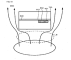
- Fig. 19 is a schematic view illustrating an example of magnetic-flux paths when the portable electronic device 800 shown in Fig. 17 is held over a RFID reader/writer.
- reference symbol ⁇ denotes a magnetic flux generated by the reader/writer.
- the portable electronic device 800 is usually held over the reader/writer such that the principal surface of a metallic casing 700 of the portable electronic device 800 is parallel to the principal surface of the reader/writer.
- magnetic-shielding objects such as the substrate 500 and the metallic casing 700 are located between the antenna coil 600 and the reader/writer in the structure shown in Patent Document 1, and the magnetic flux is blocked by the substrate 500 and the metallic casing 700. Therefore, almost no magnetic flux passes through the antenna coil. Furthermore, the axial direction of the magnetic core 601 of the antenna coil 600 is parallel to the surface of the substrate 500. Therefore, the antenna coil 600 cannot be interlinked with the magnetic flux generated by the reader/writer (magnetic flux orthogonal to the axial direction of the antenna coil 600), and cannot communicate with the reader/writer.
- the antenna coil 610 has a portion without a coil at a position where the first leg portion 611a and the second leg portion 611b of the L-shaped magnetic core 611 intersect each other at a right angle, and can be interlinked with the magnetic flux orthogonal to the axial directions at the intersecting portion.
- the magnetic resistance at end surfaces of the magnetic core 611 is large since the antenna coil 610 is disposed in the central area of the substrate. This prevents the magnetic flux from being guided into the antenna coil 610. That is, the antenna coil 610 described in Patent Document 2 also cannot be interlinked with the magnetic flux generated by the reader/writer (magnetic flux orthogonal to the axial directions of the magnetic core 611), and cannot communicate with the reader/writer.
- an object of the present invention is to provide a portable electronic device capable of appropriately being interlinked with a magnetic flux orthogonal to the axial direction of a magnetic core and capable of performing highly sensitive communication during communication with external devices such as RFID readers/writers.
- the present invention has the following structure.
- a portable electronic device includes a circuit board and an antenna coil installed on the circuit board.
- the antenna coil includes a magnetic core and a coil wound around the magnetic core and separated into a first coil portion and a second coil portion such that an unwound portion lies at the intermediate portion of the magnetic core in a longitudinal direction of the magnetic core.
- the winding directions of the first coil portion and the second coil portion differ from each other.
- the length X of the magnetic core and the distance Y between two intersecting points at which a virtual line formed by projecting the central line of the magnetic core onto the circuit board intersects the outer periphery of the circuit board satisfy Y ⁇ x ⁇ 0.8Y.
- the portable electronic device is characterized in that the distance D1 between points x1 and y1 is equal to the distance D2 between points x2 and y2, where two intersecting points at which the virtual line intersects end surfaces of the magnetic core are defined as x1 and x2, one of two intersecting points at which the virtual line intersects the outer periphery of the circuit board closer to the point x1 is defined as y1, and the other intersecting point closer to the point x2 is defined as y2.
- the portable electronic device is characterized in that the circuit board is rectangular, and the axial direction of the magnetic core corresponds to the lateral direction of the circuit board.
- the portable electronic device is characterized in that an electrode is formed on at least one surface of the magnetic core at the unwound portion.
- the portable electronic device is characterized in that the electrode has at least one slit.
- the portable electronic device is characterized in that the magnetic core has a raised portion projecting in the thickness direction of the magnetic core at the unwound portion.
- the portable electronic device is characterized in that a coil is wound around the outer periphery of the raised portion.
- the portable electronic device is characterized in that the magnetic core has at least one cut-off portion at the unwound portion.
- the portable electronic device is characterized in that the cut-off portion is formed on a surface of the magnetic core facing the circuit board.
- the portable electronic device is characterized in that the cut-off portion is formed on a side surface of the magnetic core perpendicular to the circuit board.
- the portable electronic device is characterized in that the number of turns of the first coil portion and the number of turns of the second coil portion differ from each other.
- the portable electronic device is characterized in that the antenna coil is installed over the circuit board so as to be separated from the circuit board at a distance, and the electrode is formed on the surface of the magnetic core facing the circuit board.
- a portable electronic device includes a circuit board and an antenna coil installed on the circuit board.
- the antenna coil includes a first magnetic core and a second magnetic core around which a coil is wound.
- the winding direction of a first coil portion wound around the first magnetic core differs from the winding direction of a second coil portion wound around the second magnetic core.
- the first magnetic core and the second magnetic core are juxtaposed to each other such that the axes of the first coil portion and the second coil portion correspond to each other and so as to have a gap between the first magnetic core and the second magnetic core.
- the length X of the antenna coil in the axial direction and the distance Y between two intersecting points at which a virtual line formed by projecting the central line of the antenna coil in the axial direction onto the circuit board intersects the outer periphery of the circuit board satisfy Y ⁇ x ⁇ 0.8Y.
- the portable electronic device is characterized in that the distance D1 between points x1 and y1 is equal to the distance D2 between points x2 and y2, where two intersecting points at which the virtual line intersects both end surfaces of the antenna coil in the axial direction are defined as x1 and x2, one of two intersecting points at which the virtual line intersects the outer periphery of the circuit board closer to the point x1 is defined as y1, and the other intersecting point closer to the point x2 is defined as y2.
- the portable electronic device is characterized in that the length A of the antenna coil in the axial direction and the distance B between the first magnetic core and the second magnetic core satisfy 0.6A ⁇ B ⁇ 0.4A.
- the portable electronic device is characterized in that the circuit board is rectangular, and the axial direction of the antenna coil corresponds to the lateral direction of the circuit board.
- the portable electronic device is characterized in that the antenna coil is installed over the circuit board so as to be separated from the circuit board at a distance, and an electrode is formed on surfaces of the first magnetic core and the second magnetic core facing the circuit board.
- the portable electronic device is characterized in that the first coil portion and the second coil portion are connected to each other using a conductor formed on the circuit board.
- the portable electronic device is characterized in that the first coil portion and the second coil portion are connected to each other using a conductor formed on a flexible substrate.
- the antenna coil of the portable electronic device includes a magnetic core and a coil wound around the magnetic core and separated into a first coil portion and a second coil portion such that an unwound portion lies at the intermediate portion of the magnetic core in a longitudinal direction of the magnetic core, and the winding direction of the coil is changed at either side of the unwound portion.
- the antenna coil can be interlinked with a magnetic flux that is generated by an external device such as a reader/writer and is orthogonal to the axial direction of the magnetic core during communication with the reader/writer even when the portable electronic device is held over the reader/writer such that the principal surface of the portable electronic device is parallel to the principal surface of the reader/writer, and can communicate with the reader/writer.
- the length X of the magnetic core and the distance Y between two intersecting points at which a virtual line formed by projecting the central line of the magnetic core in the axial direction onto the circuit board intersects the outer periphery of the circuit board satisfy Y ⁇ X ⁇ 0.8Y.
- the axial direction of the magnetic core preferably corresponds to the lateral direction of the circuit board.
- a larger amount of magnetic flux can be collected at the antenna coil as compared with the case where the axial direction of the magnetic core corresponds to the longitudinal direction of the circuit board. That is, part of magnetic flux that is generated by the external device and is orthogonal to the axial direction of the magnetic core is bent so as to avoid magnetic-shielding objects such as the circuit board and a metallic casing of the portable electronic device, and detours to side surfaces of the portable electronic device also in the antenna coil used in the portable electronic device according to the present invention.
- the amount of magnetic flux that detours in the lateral direction of the circuit board is larger than that of the magnetic flux that detours in the longitudinal direction since the magnetic resistance in the lateral direction is smaller than that in the longitudinal direction.
- the magnetic core disposed such that the axial direction thereof corresponds to the lateral direction of the circuit board can collect a larger amount of magnetic flux in the lateral direction of the circuit board at the antenna coil.
- the size of the antenna coil can be reduced when the axial direction of the magnetic core corresponds to the lateral direction of the circuit board.
- the magnetic core satisfies the inequality expression Y ⁇ x ⁇ 0.8Y with respect to the lateral direction of the circuit board, and the length of the magnetic core can be reduced as compared with the case where the magnetic core satisfies the above-described inequality expression with respect to the longitudinal direction. Moreover, the volume of the magnetic core can also be reduced.
- the distance D1 between points x1 and y1 is preferably equal to the distance D2 between points x2 and y2, where two intersecting points at which the virtual line intersects the end surfaces of the magnetic core are defined as x1 and x2, one of two intersecting points at which the virtual line intersects the outer periphery of the circuit board closer to the point x1 is defined as y1, and the other intersecting point closer to the point x2 is defined as y2.
- the magnetic resistance at both end surfaces of the magnetic core in the axial direction can be substantially equalized, and the amount of magnetic flux that enters the antenna coil located at either end of the unwound portion can be equalized.
- an electrode is preferably formed on at least one surface of the magnetic core at the unwound portion.
- the magnetic core preferably has a raised portion extending in the thickness direction of the magnetic core at the unwound portion.
- the magnetic core preferably has at least one cut-off portion at the unwound portion.
- paths of the magnetic flux that is orthogonal to the axial direction of the magnetic core and enters the unwound portion can be bent in the axial direction of the magnetic core more easily and reliably.
- the communication sensitivity can be further increased.
- the space inside the portable electronic device can be effectively used since the volume of the antenna coil can be reduced due to the cut-off portion.
- the cut-off portion can be formed on a surface of the magnetic core facing the circuit board at the unwound portion, or can be formed on a side surface of the magnetic core perpendicular to the circuit board at the unwound portion.
- the number of turns of the first coil portion and the number of turns of the second coil portion, the first coil portion and the second coil portion having the unwound portion being interposed between the first and second coil portions can differ from each other.
- the antenna coil can be interlinked with the magnetic flux parallel to the axial direction of the magnetic core in addition to the magnetic flux orthogonal to the axial direction of the magnetic core.
- the antenna coil can be installed over the circuit board so as to be separated from the circuit board at a distance. With this structure, the antenna coil does not come into contact with the circuit board, and does not influence the performance of the circuit formed on the circuit board.
- the antenna coil of the portable electronic device includes a first magnetic core and a second magnetic core juxtaposed to each other so as to have a gap therebetween, and the winding direction of a first coil portion wound around the first magnetic core differs from the winding direction of a second coil portion wound around the second magnetic core.
- the antenna coil can be interlinked with the magnetic flux that is generated by the external device and is orthogonal to the axial direction of the antenna coil, and can communicate with the reader/writer.
- the length X of the antenna coil and the distance Y between two intersecting points at which a virtual line formed by projecting the central line of the antenna coil in the axial direction onto the circuit board intersects the outer periphery of the circuit board satisfy Y ⁇ x ⁇ 0.8Y.
- the length A of the antenna coil in the axial direction and the distance B between the first magnetic core and the second magnetic core preferably satisfy 0.6A ⁇ B ⁇ 0.4A.
- the conductor connecting the first coil portion and the second coil portion can be formed on the circuit board, or can be formed on a flexible substrate.
- the antenna coil can be mounted on the circuit board using various methods.
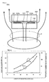
- a portable electronic device according to a first embodiment will now be described with reference to Figs. 1(A), 1(B) , and 2 .
- Figs. 1(A) and 1(B) illustrate the principal part of the portable electronic device according to the first embodiment.
- Fig. 1(A) is a perspective view
- Fig. 1(B) is a plan view.
- Fig. 2 is a schematic view illustrating an example of magnetic-flux paths when the portable electronic device shown in Figs. 1(A) and 1(B) is held over a RFID reader/writer.
- a portable electronic device 280 includes a circuit board 100 and an antenna coil 200 installed on the circuit board 100.
- the circuit board 100 is formed of a rectangular circuit substrate having a length of 90 mm and a width of 45 mm, for example.
- the antenna coil 200 includes a magnetic core 201 composed of ferrite or the like and a coil 202 wound around the outer periphery of the magnetic core 201.
- the magnetic core 201 is a rectangular parallelepiped core having a length of 45 mm, a width of 5 mm, a thickness of 2.4 mm, and a Q-factor of 100.
- the coil 202 includes a first coil portion 202a and a second coil portion 202b separately wound around the magnetic core 201 such that an unwound portion 203 lies at the intermediate portion of the magnetic core 201 in the longitudinal direction thereof.
- the winding directions of the first coil portion 202a and the second coil portion 202b differ from each other.
- the coil 202 is wound for seven turns at either side of the unwound portion 203 such that both ends of the magnetic core 201 in the longitudinal direction thereof project from the coil 202 by 1 mm.
- the magnetic core 201 has electrodes 204 formed of thin films of metal such as aluminum disposed on a side surface that faces the circuit board 100 and on both side surfaces that are perpendicular to the circuit board 100 at the unwound portion 203. That is, the electrodes 204 are formed on all side surfaces of the magnetic core 201 at the unwound portion 203 except for a side surface opposing the side surface that faces the circuit board 100.
- a magnetic flux generated by a reader/writer enters the side surface having no electrodes 204.
- reference symbol ⁇ denotes the magnetic flux generated by the reader/writer.
- the portable electronic device 280 is usually held over the reader/writer such that the principal surface of a metallic casing 300 of the portable electronic device 280 is parallel to the principal surface of the reader/writer.
- the antenna coil 200 can capture and be interlinked with the magnetic flux substantially orthogonal to the axial direction thereof since the antenna coil 200 includes the unwound portion 203 at the intermediate portion thereof.
- the magnetic flux generated by the reader/writer and entering the unwound portion 203 is bent substantially by 90° along the axial direction of the coil 202, and travels toward the first coil portion 202a and the second coil portion 202b.
- the coil 202 can capture and be interlinked with the magnetic flux that is generated by the reader/writer and is orthogonal to the axial direction of the magnetic core 201 at either the first coil portion 202a or the second coil portion 202b.
- the antenna coil can be appropriately interlinked with the magnetic flux that is generated by the reader/writer and is orthogonal to the axial direction of the magnetic core, and can perform highly sensitive communication with the reader/writer.
- the inequality expression can be satisfied. Therefore, the antenna coil 200 can be appropriately interlinked with the magnetic flux that is generated by the reader/writer and is orthogonal to the axial direction of the magnetic core 201, and can perform highly sensitive communication.
- the antenna coil 200 is disposed such that the distance D1 between points x1 and y1 is equal to the distance D2 between points x2 and y2 (herein, two intersecting points at which the virtual line intersects the end surfaces of the magnetic core 201 are defined as x1 and x2, one of two intersecting points at which the virtual line intersects the outer periphery of the circuit board 100 closer to the point x1 is defined as y1, and the other intersecting point closer to the point x2 is defined as y2). Therefore, the magnetic resistance at the end surfaces of the magnetic core 201 in the axial direction can be substantially equalized. Moreover, the amount of magnetic flux that enters the coil 202 located at either end of the unwound portion 203 can be equalized.
- the antenna coil 200 according to this embodiment is disposed such that the axial direction of the magnetic core 201 corresponds to the lateral direction of the circuit board 100.
- a larger amount of magnetic flux can be collected at the antenna coil as compared with the case where the axial direction of the magnetic core 201 corresponds to the longitudinal direction of the circuit board 100. That is, part of magnetic flux that is generated by an external device and is orthogonal to the axial direction of the magnetic core 201 is bent so as to avoid magnetic-shielding objects such as the circuit board 100 and the metallic casing 300 of the portable electronic device 280, and detours to side surfaces of the portable electronic device 280 also in this embodiment.
- the amount of magnetic flux that detours in the lateral direction of the circuit board 100 is larger than that of the magnetic flux that detours in the longitudinal direction since the magnetic resistance in the lateral direction is smaller than that in the longitudinal direction.
- the magnetic core disposed such that the axial direction thereof corresponds to the lateral direction of the circuit board 100 can collect a larger amount of magnetic flux in the lateral direction.
- the size of the antenna coil can be reduced.
- the magnetic core 201 satisfies the inequality expression Y ⁇ X ⁇ 0.8Y with respect to the lateral direction of the circuit board 100, and the length of the magnetic core 201 can be reduced as compared with the case where the magnetic core 201 satisfies the above-described inequality expression with respect to the longitudinal direction. Moreover, the volume of the magnetic core 201 can also be reduced.
- Figs. 3 to 5 illustrate changes in coupling coefficients between the antenna coil 200 and a magnetic flux generated by a reader and estimated communication ranges when the length, width, and thickness of the magnetic core 201 of the antenna coil 200 according to the first embodiment are changed from the basic dimensions.
- Figs. 3 , 4, and 5 illustrate changes in the coupling coefficients and the estimated communication ranges when the length, width, and thickness, respectively, are changed.
- the magnetic core 201 of the antenna coil 200 in this experimental example has basic dimensions of 45 mm in length, 5 mm in width, and 2.4 mm in thickness, and has a Q-factor of 100.
- the coil 202 is wound for seven turns at either side of the unwound portion 203 such that both ends of the magnetic core 201 in the longitudinal direction thereof project from the coil 202 by 1 mm.
- the circuit board 100 has a length of 90 mm, a width of 45 mm, and an electrical conductivity ⁇ of 0.60 ⁇ 10 6 .
- the antenna coil 200 is disposed such that the axial direction thereof is substantially parallel to the lateral direction of the circuit board 100.
- the antenna coil 200 can be appropriately interlinked with the magnetic flux that is generated by a reader/writer and is orthogonal to the axial direction of the magnetic core 201, and can perform highly sensitive communication when the antenna coil 200 having the basic dimensions installed on the circuit board 100 is used for communication with the reader/writer that is remote from the antenna coil 200 by 100 mm. Therefore, changes in the coupling coefficients and the estimated communication ranges when the size of the antenna coil 200 is reduced from the basic dimensions will be shown in this experimental example.
- the term "highly sensitive communication” indicates communication with a sensitivity at a level more than or equal to that required for satisfying market needs.
- the term indicates communication with a coupling coefficient of 0.18% or more when the distance between the antenna coil 200 and the reader/writer is 100 mm. That is, when the coupling coefficient is 0.18% or more, the antenna coil can ensure a communication range of 100 mm.
- the magnetic core 201 of the antenna coil 200 shown in Fig. 3 has a length ranging from 10 to 45 mm, a width of 5 mm, and a thickness of 2.4 mm.
- the magnetic core 201 of the antenna coil 200 shown in Fig. 4 has a length of 45 mm, a width ranging from 2 to 5 mm, and a thickness of 2.4 mm.
- the magnetic core 201 of the antenna coil 200 shown in Fig. 5 has a length of 45 mm, a width of 5 mm, and a thickness ranging from 1.2 to 2.4 mm.
- the coupling coefficient is reduced in proportion to the length of the magnetic core 201.
- the coupling coefficient is reduced to 0.12%, and only the estimated communication range of 87 mm can be ensured. Therefore, when the length of the magnetic core 201 is reduced to 30 mm, communication sensitivity at the level required for satisfying market needs cannot be achieved.
- the coupling coefficient is not markedly changed even when the width of the magnetic core 201 is reduced. This indicates that excellent communication can be ensured.
- the coupling coefficient of 0.28% can be achieved even when the width is set to 2 mm, and the estimated communication range of 100 mm or more can be ensured.
- the coupling coefficient is not markedly changed even when the thickness, i.e., height, of the magnetic core 201 is reduced. This indicates that excellent communication can be ensured.
- the coupling coefficient of 0.30% can be achieved even when the thickness is set to 1.2 mm, and an amount of coupling that ensures the estimated communication range of 100 mm or more can be achieved.
- the experimental results shown in Figs. 3 to 5 show that the most influential dimension in the amount of coupling between the antenna coil 200 and the magnetic flux of the reader/writer is the length of the magnetic core 201 among the length, width, and thickness of the magnetic core 201. Moreover, it is shown that the coupling coefficient of 0.18% or more can be achieved by setting the length of the magnetic core 201 of the antenna coil 200 to at least 36 mm, and the antenna coil 200 can perform highly sensitive communication with the reader/writer at a level more than or equal to that required for satisfying market needs.
- the experimental results show that when the distance X between two intersecting points at which the central line of the magnetic core 201 in the axial direction intersects end surfaces of the magnetic core 201 and the distance Y between two intersecting points at which the virtual line formed by projecting the central line onto the circuit board 100 intersects the outer periphery of the circuit board 100 shown satisfy Y ⁇ X ⁇ 0.8Y, the antenna coil 200 can be appropriately interlinked with the magnetic flux generated by the reader/writer (magnetic flux orthogonal to the axial direction of the magnetic core 201), and can perform highly sensitive communication.
- the lower limit of X (X ⁇ 0.8Y) indicates the minimum length of the magnetic core required for ensuring the coupling coefficient of 0.18% or more determined from the drawing, and the upper limit of X (B ⁇ A) is set to the same length as that of the circuit board 200 in the lateral direction.
- the electrodes 204 are formed on all the side surfaces of the magnetic core 201 at the unwound portion 203 except for the side surface opposing the side surface that faces the circuit board 100, that is, formed on the side surface that faces the circuit board 100 and on both side surfaces that are perpendicular to the circuit board 100.
- the present invention is not limited to this embodiment.
- the electrodes 204 can be formed on side surfaces of the magnetic core 201 at the unwound portion 203 except for at least one side surface into which the magnetic flux travels.
- the electrodes 204 are not necessarily formed in the present invention. However, the electrodes 204 are preferably formed from the viewpoint of increasing the communication sensitivity.
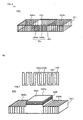
- each of the electrodes 204 can have a ladder shape including a plurality of rung portions 204a and stile portions 204b that connect the rung portions 204a.
- the ladder-shaped electrodes 204 each have a plurality of slits 207. Since the length of current paths can be changed by trimming parts of the stile portions 204b off as shown in Fig. 6(B) , the inductance of the coil 202 can be easily adjusted.
- Each of the electrodes 204 preferably has at least one slit 207 since the inductance of the coil 202 can be easily changed by changing the length of the current paths using trimming.
- the magnetic core 201 is a rectangular parallelepiped.
- the present invention is not limited to this embodiment, and the magnetic core 201 can have other shapes, for example, a cylindrical shape or a triangular prismatic shape.
- the magnetic core 201 can have a raised portion 203a projecting in the thickness direction at the unwound portion 203, and a coil 205 can be wound around the raised portion 203a.
- the ability to collect the magnetic flux of the magnetic core 201 can be enhanced such that a larger amount of magnetic flux can be guided into the antenna coil 201.
- the electromotive force can be increased, and the communication sensitivity can be further increased.
- the antenna coil 200 according to the present invention can have a cut-off portion 206 formed on the side surface of the magnetic core 201, the side surface facing the circuit board.
- the cut-off portion 206 shown in Fig. 8 is formed by cutting a triangular prismatic portion off the magnetic core 201.
- the cut-off portion 206 can be formed by cutting a rectangular parallelepiped portion off the magnetic core 201.
- the cut-off portion 206 is formed on the side surface that faces the circuit board.
- a gap is formed between the antenna coil 200 and the circuit board at the central portion of the antenna coil 200, and the space formed by the gap can be effectively used.
- the cut-off portion 206 shown in Fig. 10 is formed on a side surface perpendicular to the circuit board.
- a recessed portion where no magnetic core lies is formed on the board at the central portion of the antenna coil 200, and other components disposed on the circuit board can extend toward this portion.
- flexibility in designing the circuit board on which the antenna coil 200 is mounted can be improved.
- the number of turns of the first coil portion 202a and the number of turns of the second coil portion 202b, the unwound portion 203 being interposed between the coil portions 202a and 202b can differ from each other.
- the ratio of the number of turns of the first coil portion 202a to the number of turns of the second coil portion 202b, the unwound portion 203 being interposed between the coil portions 202a and 202b is, for example, 1:2 in the coil 202 as shown in Figs.
- the antenna coil 200 can be interlinked with the magnetic flux parallel to the axial direction of the magnetic core 201 in addition to the magnetic flux orthogonal to the axial direction of the magnetic core 201. That is, when a magnetic flux orthogonal to the axial direction of the magnetic core 201 passes through the antenna coil 200, a current A and a current B flowing in the same direction are generated at the first coil portion 202a and the second coil portion 202b, respectively, as shown in Fig. 11(A) .
- a current A and a current B flowing in directions opposite to each other are generated at the first coil portion 202a and the second coil portion 202b, respectively, as shown in Fig. 11(B) .
- the ratio of the number of turns of the first coil portion 202a to the number of turns of the second coil portion 202b, the unwound portion 203 being interposed between the coil portions 202a and 202b is 1:2, i.e., not one, the amounts of currents A and B flowing in directions opposite to each other differ from each other, and the currents A and B do not cancel each other completely.
- the antenna coil 200 can reliably capture the magnetic flux generated by the reader/writer, and can communicate with the reader/writer.
- the ratio of the number of turns of the first coil portion 202a to the number of turns of the second coil portion 202b is not limited to 1:2, and may be any value as long as the number of turns of the first coil portion 202a and that of the second coil portion 202b differ from each other.
- the first coil portion 202a and the second coil portion 202b can be disposed in parallel.
- a portable electronic device according to a second embodiment will now be described with reference to Fig. 12 .
- Fig. 12 is a front view of the portable electronic device according to the second embodiment.
- descriptions of components common to or corresponding to those shown in Fig. 1 illustrating the first embodiment will be omitted as appropriate.
- a portable electronic device 280 includes a circuit board 100 and an antenna coil 200 installed over the circuit board 100.
- the antenna coil 200 is installed over the circuit board 100 so as to be separated from the circuit board 100 at a predetermined distance.
- the antenna coil 200 is installed over the circuit board 100 at a predetermined distance from the circuit board 100 by, for example, being bonded to a casing located above the circuit board 100.
- the circuit board 100 and the antenna coil 200 have a predetermined gap therebetween in this manner, the antenna coil 200 does not come into contact with the circuit board 100, and does not influence the performance of the circuit.
- flexibility in the layout of the antenna coil 200 can be improved since the antenna coil 200 does not come into contact with the circuit board 100.
- the antenna coil 200 includes a magnetic core 201. As shown in Fig. 12 , an electrode 208 is formed so as to cover the entire surface of the magnetic core 201 facing the circuit board 100. In order to avoid connection of the electrode 208 to a first coil portion 202a and a second coil portion 202b, the electrode 208 is formed on the surface of the magnetic core 201 facing the circuit board 100 after a nonconductive adhesive or the like is applied to the surface.
- the electrode 208 formed on the surface of the magnetic core 201 facing the circuit board 100 in this manner can prevent the magnetic flux that enters the magnetic core 201 from leaking into the gap between the magnetic core 201 and the circuit board 100. Thus, reduction in communication sensitivity can be regulated even when a predetermined gap is formed between the circuit board 100 and the antenna coil 200.
- the electrode 208 is formed so as to cover the entire surface of the magnetic core 201 facing the circuit board 100 in the second embodiment, but can be formed so as to cover a part of the surface. However, a larger electrode 208 is preferably formed since the larger electrode 208 can prevent the magnetic flux entering the magnetic core 201 from leaking into the gap between the magnetic core 201 and the circuit board 100 more easily.
- a portable electronic device according to a third embodiment will now be described with reference to Figs. 13(A) and 13(B) .
- Figs. 13(A) and 13(B) illustrate the principal part of the portable electronic device according to the third embodiment.
- Fig. 13(A) is a perspective view
- Fig. 13(B) is a plan view.
- a portable electronic device 480 includes a circuit board 300 and an antenna coil 400 installed on the circuit board 300.
- the circuit board 300 is formed of a rectangular circuit substrate having a length of 90 mm and a width of 45 mm, for example.
- the antenna coil 400 is disposed on the circuit board 300 such that the axial direction of the antenna coil 400 corresponds to the lateral direction of the circuit board 300.
- the axial direction of the antenna coil corresponds to the axial directions of magnetic cores (described below).
- the antenna coil 400 includes a first magnetic core 401a and a second magnetic core 401b composed of ferrite or the like.
- the magnetic cores 401a and 401b are rectangular parallelepiped cores each having a length of 10 mm, a width of 7 mm, a thickness of 1.5 mm, and a Q-factor of 100.
- the first magnetic core 401a and the second magnetic core 401b are juxtaposed to each other such that the axes thereof correspond to each other and so as to have a gap therebetween.
- the size of the gap is 26 mm.
- a coil wound around the first magnetic core 401a and the second magnetic core 401b constitutes a first coil portion 402a and a second coil portion 402b, respectively.
- the first coil portion 402a is wound for six turns such that both ends of the first magnetic core in the axial direction thereof project from the first coil portion 402a by 1 mm.
- the second coil portion 402b has the same structure as that of the first coil portion 402a.
- the winding directions of the first coil portion 402a and the second coil portion 402b differ from each other.
- coils are wound around the magnetic cores 401a and 401b such that the lateral directions of the magnetic cores correspond to the axial directions of the coils.
- the antenna coil 400 can capture and be interlinked with a magnetic flux substantially orthogonal to the axial direction of the antenna coil. That is, since the winding directions of the first coil portion 402a and the second coil portion 402b differ from each other, the magnetic flux generated by the reader/writer and entering the gap between the first magnetic core 401a and the second magnetic core 401b (magnetic flux orthogonal to the axial direction of the antenna coil) is bent substantially by 90° along the axial direction of the first magnetic core 401a and the second magnetic core 401b.
- the antenna coil can capture and be interlinked with the magnetic flux that is generated by the reader/writer and is orthogonal to the axial direction of the antenna coil at either the first magnetic core 401a or the second magnetic core 401b.
- the antenna coil 400 has a gap between the first magnetic core 401a and the second magnetic core 401b, and other components disposed on the circuit board 300 can extend toward the gap.
- flexibility in designing the circuit board 300 on which the antenna coil 400 is mounted can be improved.
- the antenna coil can be appropriately interlinked with the magnetic flux that is generated by the reader/writer and is orthogonal to the axial direction of the magnetic cores, and can perform highly sensitive communication with the reader/writer.
- the inequality expression can be satisfied since the length X of the antenna coil 400 in the axial direction thereof is 40 mm and the distance Y between the two intersecting points at which the virtual line formed by projecting the central line of the antenna coil 400 in the axial direction onto the circuit board intersects the outer periphery of the circuit board is 45 mm. Therefore, the antenna coil 400 can be appropriately interlinked with the magnetic flux that is generated by the reader/writer and is orthogonal to the axial direction of the antenna coil 400, and can perform highly sensitive communication with the reader/writer.
- the antenna coil 400 is disposed such that the distance D1 between points x1 and y1 is equal to the distance D2 between points x2 and y2 (herein, two intersecting points at which the virtual line intersects the end surfaces of the antenna coil 400 are defined as x1 and x2, one of two intersecting points at which the virtual line intersects the outer periphery of the circuit board 300 closer to the point x1 is defined as y1, and the other intersecting point closer to the point x2 is defined as y2). Therefore, the magnetic resistance at the end surfaces of the antenna coil 400 in the axial direction can be substantially equalized. Moreover, the amount of magnetic flux that enters the gap between the first magnetic core 401a and the second magnetic core 401b can be equalized.
- the antenna coil 400 according to this embodiment is disposed such that the axial direction of the antenna coil 400 corresponds to the lateral direction of the circuit board 300. With this arrangement, a larger amount of magnetic flux can be collected at the antenna coil as compared with the case where the axial direction of the antenna coil 400 corresponds to the longitudinal direction of the circuit board 300.
- the portable electronic device 480 includes the first magnetic core 401a and the second magnetic core 401b juxtaposed to each other so as to have a gap therebetween.
- a larger gap prevents the magnetic flux from being guided into the first magnetic core 401a and the second magnetic core 401b, and the amount of magnetic flux penetrating through the axes of the first coil portion 402a and the second coil portion 402b is reduced.
- the distance between the first magnetic core 401a and the second magnetic core 401b is preferably set to a predetermined length.
- the antenna coil 400 can be appropriately interlinked with the magnetic flux that is generated by the reader/writer and is orthogonal to the axial direction of the antenna coil 400, and can perform highly sensitive communication. Therefore, it is preferable that the distance between the first magnetic core 401a and the second magnetic core 401b is set in accordance with this condition.
- the above-described condition is satisfied since the length A of the antenna coil 400 in the axial direction is 40 mm, and the distance B between the first magnetic core 401a and the second magnetic core 401b is 26 mm. Therefore, the antenna coil 400 can be appropriately interlinked with the magnetic flux that is generated by the reader/writer and is orthogonal to the axial direction of the antenna coil 400, and can perform highly sensitive communication with the reader/writer.
- the number of turns of the first coil portion 402a and the number of turns of the second coil portion 402b are the same. However, the number of turns of the first coil portion 402a and the number of turns of the second coil portion 402b can differ from each other. When the numbers of turns of the first coil portion 402a and the second coil portion 402b differ from each other, the antenna coil 400 can be interlinked with a magnetic flux parallel to the axial direction of the antenna coil 400 in addition to that orthogonal to the axial direction of the antenna coil 480.
- a portable electronic device according to a fourth embodiment will now be described with reference to Fig. 14 .
- Fig. 14 is a front view of the portable electronic device according to the fourth embodiment.
- descriptions of components common to or corresponding to those shown in Fig. 13 illustrating the third embodiment will be omitted as appropriate.
- a portable electronic device 480 includes a circuit board 300 and an antenna coil 400 installed over the circuit board 300.
- the antenna coil 400 is installed over the circuit board 300 so as to be separated from the circuit board 300 at a predetermined distance.
- the antenna coil 400 is installed over the circuit board 300 at a predetermined distance from the circuit board 300 by, for example, being bonded to a casing located above the circuit board 300.
- the antenna coil 400 does not come into contact with the circuit board 300, and does not influence the performance of the circuit formed on the circuit board 300.
- flexibility in the layout of the antenna coil 400 can be improved since the antenna coil 400 does not come into contact with the circuit board 300.
- the antenna coil 400 includes a first magnetic core 401a and a second magnetic core 401b. As shown in Fig. 14 , an electrode 408 is formed so as to cover surfaces of the first magnetic core 401a and the second magnetic core 401b facing the circuit board 300. In order to avoid connection of the electrode 407 to a first coil portion 402a and a second coil portion 402b, the electrode 408 is formed on the surfaces of the first magnetic core 401a and the second magnetic core 401b facing the circuit board 300 after a nonconductive adhesive or the like is applied to the surfaces.
- the electrode 408 formed on the surfaces of the first magnetic core 401a and the second magnetic core 401b facing the circuit board 300 in this manner can prevent the magnetic flux that enters the first magnetic core 401a and the second magnetic core 401b from leaking into the gap between the antenna coil 400 and the circuit board 300.
- reduction in communication sensitivity can be regulated even when a predetermined gap is formed between the circuit board 300 and the magnetic cores 401a and 401b.
- a portable electronic device according to a fifth embodiment will now be described with reference to Fig. 15 .
- Fig. 15 is a partially enlarged view of the portable electronic device according to the fifth embodiment.
- descriptions of components common to or corresponding to those shown in Fig. 13 illustrating the third embodiment will be omitted as appropriate.
- a portable electronic device 480 includes a first coil portion 402a and a second coil portion 402b connected using a connecting conductor 460 formed on a circuit board 300.
- the first coil portion 402a and the second coil portion 402b can be connected by only mounting an antenna coil 400 on the circuit board 300 due to the connecting conductor 460 formed on the circuit board 300. This can facilitate the production of the portable electronic device 480.
- the connecting conductor 460 can be formed on a circuit board other than the circuit board 300 on which the antenna coil 400 is mounted.
- Fig. 16 illustrates a modification of the portable electronic device 480 according to the fifth embodiment.
- the first coil portion 402a and the second coil portion 402b can be connected to each other using the connecting conductor 460 formed on a flexible substrate 470.
- the flexible substrate 470 can be formed of a foldable electrically insulating film such as a resin film including a polyimide film and a glass epoxy film.
- the connecting conductor 460 for connecting the first coil portion 402a and the second coil portion 402b is formed on the flexible substrate 470.
- a connecting conductor for connection to an input terminal and a connecting conductor for connection to an output terminal are also formed on the flexible substrate 470.
- the coil portions 402a and 402b can be easily connected to the input/output terminals by only connecting the flexible substrate 470 to the input/output terminals due to the connecting conductors for connection to the input terminal and the output terminal formed on the flexible substrate 470.
- a first magnetic core 401a around which the first coil portion 402a is wound and a second magnetic core 401b around which the second coil portion 402b is wound are bonded to the flexible substrate 470 using an adhesive, and the first coil portion 402a and the second coil portion 402b are soldered to the connecting conductor 460. In this manner, the first coil portion 402a and the second coil portion 402b are connected to each other via the connecting conductor 460.
- the first magnetic core 401a and the second magnetic core 402b are integrated with each other on the flexible substrate 470 by bonding the first magnetic core 401a and second magnetic core 401b to the flexible substrate 470, and can be easily mounted on the circuit board 300.
- the first magnetic core 401a and the second magnetic core 401b are integrated with each other on the flexible substrate 470 in advance, there is no need to adjust the distance between the first magnetic core 401a and the second magnetic core 401b on the circuit board 300. In other words, the sensitivity of the antenna coil 400 is not changed due to the fixed distance between the first magnetic core 401a and the second magnetic core 401b.
- End portions of the connecting conductor 460 formed on the flexible substrate 470 can have certain widths.
- connecting positions at which the connecting conductor 460 is connected to the first coil portion 402a and the second coil portion 402b can be arbitrarily selected within the widths of end portions of the connecting conductor 460. With this, the distance between the first magnetic core 401a and the second magnetic core 401b can be easily adjusted on the flexible substrate 470.
Landscapes
- Support Of Aerials (AREA)
- Near-Field Transmission Systems (AREA)
- Coils Or Transformers For Communication (AREA)
- Telephone Set Structure (AREA)
Abstract
Description
- The present invention relates to portable electronic devices for, for example, portable telephone terminals having wireless tags for RFID (Radio Frequency Identification) used for communication with external devices via electromagnetic-field signals.
- Portable electronic devices such as cellular phones having RFID wireless tags have come into widespread use in recent years, and some of which include antenna coils for wireless tags as described in, for example,
Patent Document 1.Fig. 17 is a perspective view illustrating the principal part of a portableelectronic device 800 shown inPatent Document 1.Fig. 17 illustrates the structure of the portableelectronic device 800 including asubstrate 500 and acylindrical antenna coil 600 having amagnetic core 601 disposed on thesubstrate 500. Theantenna coil 600 is disposed such that the axial direction thereof is parallel to the surface of thesubstrate 500, and can be interlinked with a magnetic flux parallel to the surface of thesubstrate 500. - Moreover,
Patent Document 2 shown inFig. 18 discloses a portableelectronic device 810 capable of being interlinked with a magnetic flux parallel to the surface of asubstrate 510 in all directions by disposing anantenna coil 610 including an L-shaped magnetic core 611 formed of afirst leg portion 611a and asecond leg portion 611b on thesubstrate 510. - Patent Document 1: Japanese Unexamined Patent Application Publication No.
2003-16409 - Patent Document 2: Japanese Unexamined Patent Application Publication No.
10-242742 -
Fig. 19 is a schematic view illustrating an example of magnetic-flux paths when the portableelectronic device 800 shown inFig. 17 is held over a RFID reader/writer. InFig. 19 , reference symbol φ denotes a magnetic flux generated by the reader/writer. As shown inFig. 19 , the portableelectronic device 800 is usually held over the reader/writer such that the principal surface of ametallic casing 700 of the portableelectronic device 800 is parallel to the principal surface of the reader/writer. - However, magnetic-shielding objects such as the
substrate 500 and themetallic casing 700 are located between theantenna coil 600 and the reader/writer in the structure shown inPatent Document 1, and the magnetic flux is blocked by thesubstrate 500 and themetallic casing 700. Therefore, almost no magnetic flux passes through the antenna coil. Furthermore, the axial direction of themagnetic core 601 of theantenna coil 600 is parallel to the surface of thesubstrate 500. Therefore, theantenna coil 600 cannot be interlinked with the magnetic flux generated by the reader/writer (magnetic flux orthogonal to the axial direction of the antenna coil 600), and cannot communicate with the reader/writer. - Similarly, almost no magnetic flux orthogonal to the axial directions of the magnetic core 611 passes through the
antenna coil 610 shown inPatent Document 2 since the magnetic flux is blocked by the substrate and the metallic casing. Theantenna coil 610 has a portion without a coil at a position where thefirst leg portion 611a and thesecond leg portion 611b of the L-shaped magnetic core 611 intersect each other at a right angle, and can be interlinked with the magnetic flux orthogonal to the axial directions at the intersecting portion. However, the magnetic resistance at end surfaces of the magnetic core 611 is large since theantenna coil 610 is disposed in the central area of the substrate. This prevents the magnetic flux from being guided into theantenna coil 610. That is, theantenna coil 610 described inPatent Document 2 also cannot be interlinked with the magnetic flux generated by the reader/writer (magnetic flux orthogonal to the axial directions of the magnetic core 611), and cannot communicate with the reader/writer. - Accordingly, an object of the present invention is to provide a portable electronic device capable of appropriately being interlinked with a magnetic flux orthogonal to the axial direction of a magnetic core and capable of performing highly sensitive communication during communication with external devices such as RFID readers/writers.
- To solve the above-described problems, the present invention has the following structure.
- According to the invention as claimed in
Claim 1, a portable electronic device includes a circuit board and an antenna coil installed on the circuit board. The antenna coil includes a magnetic core and a coil wound around the magnetic core and separated into a first coil portion and a second coil portion such that an unwound portion lies at the intermediate portion of the magnetic core in a longitudinal direction of the magnetic core. The winding directions of the first coil portion and the second coil portion differ from each other. The length X of the magnetic core and the distance Y between two intersecting points at which a virtual line formed by projecting the central line of the magnetic core onto the circuit board intersects the outer periphery of the circuit board satisfy Y ≥ x ≥ 0.8Y. - According to the invention as claimed in
Claim 2, which is dependent onClaim 1, the portable electronic device is characterized in that the distance D1 between points x1 and y1 is equal to the distance D2 between points x2 and y2, where two intersecting points at which the virtual line intersects end surfaces of the magnetic core are defined as x1 and x2, one of two intersecting points at which the virtual line intersects the outer periphery of the circuit board closer to the point x1 is defined as y1, and the other intersecting point closer to the point x2 is defined as y2. - According to the invention as claimed in
Claim 3, which is dependent onClaim - According to the invention as claimed in
Claim 4, which is dependent on any one ofClaims 1 to 3, the portable electronic device is characterized in that an electrode is formed on at least one surface of the magnetic core at the unwound portion. - According to the invention as claimed in Claim 5, which is dependent on
Claim 4, the portable electronic device is characterized in that the electrode has at least one slit. - According to the invention as claimed in Claim 6, which is dependent on any one of
Claims 1 to 5, the portable electronic device is characterized in that the magnetic core has a raised portion projecting in the thickness direction of the magnetic core at the unwound portion. - According to the invention as claimed in Claim 7, which is dependent on Claim 6, the portable electronic device is characterized in that a coil is wound around the outer periphery of the raised portion.
- According to the invention as claimed in Claim 8, which is dependent on any one of
Claims 1 to 7, the portable electronic device is characterized in that the magnetic core has at least one cut-off portion at the unwound portion. - According to the invention as claimed in Claim 9, which is dependent on Claim 8, the portable electronic device is characterized in that the cut-off portion is formed on a surface of the magnetic core facing the circuit board.
- According to the invention as claimed in
Claim 10, which is dependent on Claim 8 or 9, the portable electronic device is characterized in that the cut-off portion is formed on a side surface of the magnetic core perpendicular to the circuit board. - According to the invention as claimed in Claim 11, which is dependent on any one of
Claims 1 to 10, the portable electronic device is characterized in that the number of turns of the first coil portion and the number of turns of the second coil portion differ from each other. - According to the invention as claimed in Claim 12, which is dependent on any one of
Claims 1 to 11, the portable electronic device is characterized in that the antenna coil is installed over the circuit board so as to be separated from the circuit board at a distance, and the electrode is formed on the surface of the magnetic core facing the circuit board. - According to the invention as claimed in Claim 13, a portable electronic device includes a circuit board and an antenna coil installed on the circuit board. The antenna coil includes a first magnetic core and a second magnetic core around which a coil is wound. The winding direction of a first coil portion wound around the first magnetic core differs from the winding direction of a second coil portion wound around the second magnetic core. The first magnetic core and the second magnetic core are juxtaposed to each other such that the axes of the first coil portion and the second coil portion correspond to each other and so as to have a gap between the first magnetic core and the second magnetic core. The length X of the antenna coil in the axial direction and the distance Y between two intersecting points at which a virtual line formed by projecting the central line of the antenna coil in the axial direction onto the circuit board intersects the outer periphery of the circuit board satisfy Y ≥ x ≥ 0.8Y.
- According to the invention as claimed in Claim 14, which is dependent on Claim 13, the portable electronic device is characterized in that the distance D1 between points x1 and y1 is equal to the distance D2 between points x2 and y2, where two intersecting points at which the virtual line intersects both end surfaces of the antenna coil in the axial direction are defined as x1 and x2, one of two intersecting points at which the virtual line intersects the outer periphery of the circuit board closer to the point x1 is defined as y1, and the other intersecting point closer to the point x2 is defined as y2.
- According to the invention as claimed in Claim 15, which is dependent on Claim 13 or 14, the portable electronic device is characterized in that the length A of the antenna coil in the axial direction and the distance B between the first magnetic core and the second magnetic core satisfy 0.6A ≥ B ≥ 0.4A.
- According to the invention as claimed in Claim 16, which is dependent on any one of Claims 13 to 15, the portable electronic device is characterized in that the circuit board is rectangular, and the axial direction of the antenna coil corresponds to the lateral direction of the circuit board.
- According to the invention as claimed in Claim 17, which is dependent on any one of Claims 13 to 16, the portable electronic device is characterized in that the antenna coil is installed over the circuit board so as to be separated from the circuit board at a distance, and an electrode is formed on surfaces of the first magnetic core and the second magnetic core facing the circuit board.
- According to the invention as claimed in Claim 18, which is dependent on any one of Claims 13 to 17, the portable electronic device is characterized in that the first coil portion and the second coil portion are connected to each other using a conductor formed on the circuit board.
- According to the invention as claimed in Claim 19, which is dependent on any one of Claims 13 to 18, the portable electronic device is characterized in that the first coil portion and the second coil portion are connected to each other using a conductor formed on a flexible substrate.
- According to the present invention, the following effects can be obtained.
- According to a first invention, the antenna coil of the portable electronic device includes a magnetic core and a coil wound around the magnetic core and separated into a first coil portion and a second coil portion such that an unwound portion lies at the intermediate portion of the magnetic core in a longitudinal direction of the magnetic core, and the winding direction of the coil is changed at either side of the unwound portion. With this structure, the antenna coil can be interlinked with a magnetic flux that is generated by an external device such as a reader/writer and is orthogonal to the axial direction of the magnetic core during communication with the reader/writer even when the portable electronic device is held over the reader/writer such that the principal surface of the portable electronic device is parallel to the principal surface of the reader/writer, and can communicate with the reader/writer. Moreover, the length X of the magnetic core and the distance Y between two intersecting points at which a virtual line formed by projecting the central line of the magnetic core in the axial direction onto the circuit board intersects the outer periphery of the circuit board satisfy Y ≥ X ≥ 0.8Y. With this structure, the magnetic resistance of the magnetic core can be reduced by bringing the end surfaces of the magnetic core in the axial direction close to the outer periphery of the circuit board. Thus, the magnetic flux can be collected at the antenna coil, and the antenna coil can be appropriately interlinked with the magnetic flux orthogonal to the axial direction of the magnetic core. In this manner, the communication sensitivity can be further increased.
- When the circuit board is rectangular, the axial direction of the magnetic core preferably corresponds to the lateral direction of the circuit board. With this arrangement, a larger amount of magnetic flux can be collected at the antenna coil as compared with the case where the axial direction of the magnetic core corresponds to the longitudinal direction of the circuit board. That is, part of magnetic flux that is generated by the external device and is orthogonal to the axial direction of the magnetic core is bent so as to avoid magnetic-shielding objects such as the circuit board and a metallic casing of the portable electronic device, and detours to side surfaces of the portable electronic device also in the antenna coil used in the portable electronic device according to the present invention. At this moment, the amount of magnetic flux that detours in the lateral direction of the circuit board is larger than that of the magnetic flux that detours in the longitudinal direction since the magnetic resistance in the lateral direction is smaller than that in the longitudinal direction. Thus, the magnetic core disposed such that the axial direction thereof corresponds to the lateral direction of the circuit board can collect a larger amount of magnetic flux in the lateral direction of the circuit board at the antenna coil. Moreover, the size of the antenna coil can be reduced when the axial direction of the magnetic core corresponds to the lateral direction of the circuit board. That is, the magnetic core satisfies the inequality expression Y ≥ x ≥ 0.8Y with respect to the lateral direction of the circuit board, and the length of the magnetic core can be reduced as compared with the case where the magnetic core satisfies the above-described inequality expression with respect to the longitudinal direction. Moreover, the volume of the magnetic core can also be reduced.
- Moreover, the distance D1 between points x1 and y1 is preferably equal to the distance D2 between points x2 and y2, where two intersecting points at which the virtual line intersects the end surfaces of the magnetic core are defined as x1 and x2, one of two intersecting points at which the virtual line intersects the outer periphery of the circuit board closer to the point x1 is defined as y1, and the other intersecting point closer to the point x2 is defined as y2. With this structure, the magnetic resistance at both end surfaces of the magnetic core in the axial direction can be substantially equalized, and the amount of magnetic flux that enters the antenna coil located at either end of the unwound portion can be equalized.
- Moreover, an electrode is preferably formed on at least one surface of the magnetic core at the unwound portion. With this structure, the magnetic flux can be prevented from leaking and can be guided into the antenna coil, resulting in an increase in the electromotive force of the antenna coil. The electrode preferably has a slit since the inductance of the coil can be easily adjusted.
- Moreover, the magnetic core preferably has a raised portion extending in the thickness direction of the magnetic core at the unwound portion. With this structure, the ability to collect the magnetic flux of the antenna coil can be enhanced, and the electromotive force of the antenna coil can be increased. Furthermore, the ability to collect the magnetic flux can be further increased when a coil is wound around the raised portion.
- Moreover, the magnetic core preferably has at least one cut-off portion at the unwound portion. With this structure, paths of the magnetic flux that is orthogonal to the axial direction of the magnetic core and enters the unwound portion can be bent in the axial direction of the magnetic core more easily and reliably. Thus, the communication sensitivity can be further increased. According to another effect of this structure, the space inside the portable electronic device can be effectively used since the volume of the antenna coil can be reduced due to the cut-off portion. The cut-off portion can be formed on a surface of the magnetic core facing the circuit board at the unwound portion, or can be formed on a side surface of the magnetic core perpendicular to the circuit board at the unwound portion.
- Moreover, the number of turns of the first coil portion and the number of turns of the second coil portion, the first coil portion and the second coil portion having the unwound portion being interposed between the first and second coil portions, can differ from each other. With this structure, the antenna coil can be interlinked with the magnetic flux parallel to the axial direction of the magnetic core in addition to the magnetic flux orthogonal to the axial direction of the magnetic core.
- Moreover, the antenna coil can be installed over the circuit board so as to be separated from the circuit board at a distance. With this structure, the antenna coil does not come into contact with the circuit board, and does not influence the performance of the circuit formed on the circuit board.
- Moreover, according to a second invention, the antenna coil of the portable electronic device includes a first magnetic core and a second magnetic core juxtaposed to each other so as to have a gap therebetween, and the winding direction of a first coil portion wound around the first magnetic core differs from the winding direction of a second coil portion wound around the second magnetic core. With this structure, the antenna coil can be interlinked with the magnetic flux that is generated by the external device and is orthogonal to the axial direction of the antenna coil, and can communicate with the reader/writer. Moreover, the length X of the antenna coil and the distance Y between two intersecting points at which a virtual line formed by projecting the central line of the antenna coil in the axial direction onto the circuit board intersects the outer periphery of the circuit board satisfy Y ≥ x ≥ 0.8Y. With this structure, the magnetic resistance of the antenna coil can be reduced by bringing the end surfaces of the antenna coil in the axial direction close to the outer periphery of the circuit board. Thus, the magnetic flux can be collected at the antenna coil, and the antenna coil can be appropriately interlinked with the magnetic flux orthogonal to the axial direction of the antenna coil. In this manner, the communication sensitivity can be further increased.
- Moreover, the length A of the antenna coil in the axial direction and the distance B between the first magnetic core and the second magnetic core preferably satisfy 0.6A ≥ B ≥ 0.4A. With this structure, the communication sensitivity is not markedly degraded even when the first magnetic core and the second magnetic core are juxtaposed to each other so as to have a gap therebetween.
- Moreover, the conductor connecting the first coil portion and the second coil portion can be formed on the circuit board, or can be formed on a flexible substrate. With these structures, the antenna coil can be mounted on the circuit board using various methods.
-
- [
Fig. 1] Figs. 1(A) and 1(B) illustrate the principal part of a portable electronic device according to a first embodiment. - [
Fig. 2] Fig. 2 is a schematic view illustrating an example of magnetic-flux paths when the portable electronic device shown inFigs. 1(A) and 1(B) is held over a RFID reader/writer. - [
Fig. 3] Fig. 3 illustrates changes in a coupling coefficient and an estimated communication range when the length of a magnetic core of an antenna coil according to the first embodiment is changed from a basic dimension. [Fig. 4] Fig. 4 illustrates changes in the coupling coefficient and the estimated communication range when the width of the magnetic core of the antenna coil according to the first embodiment is changed from the basic dimension. [Fig. 5] Fig. 5 illustrates changes in the coupling coefficient and the estimated communication range when the thickness of the magnetic core of the antenna coil according to the first embodiment is changed from the basic dimension. [Fig. 6] Figs. 6(A) and 6(B) illustrate a modification of the antenna coil according to the first embodiment. - [
Fig. 7] Fig. 7 is a perspective view of another modification of the antenna coil according to the first embodiment. - [
Fig. 8] Fig. 8 is a perspective view of another modification of the antenna coil according to the first embodiment. - [
Fig. 9] Fig. 9 is a perspective view of another modification of the antenna coil according to the first embodiment. - [
Fig. 10] Fig. 10 is a perspective view of another modification of the antenna coil according to the first embodiment. - [
Fig. 11] Figs. 11(A) and 11(B) are perspective views illustrating another modification of the antenna coil according to the first embodiment. - [
Fig. 12] Fig. 12 is a front view illustrating the principal part of a portable electronic device according to a second embodiment. - [
Fig. 13] Figs. 13(A) and 13(B) illustrate the principal part of a portable electronic device according to a third embodiment. - [
Fig. 14] Fig. 14 is a front view illustrating the principal part of a portable electronic device according to a fourth embodiment. - [
Fig. 15] Fig. 15 is a perspective view illustrating the principal part of a portable electronic device according to a fifth embodiment. - [
Fig. 16] Fig. 16 is a perspective view illustrating a modification of the portable electronic device according to the fifth embodiment. - [
Fig. 17] Fig. 17 is a perspective view illustrating the principal part of a portable electronic device according to a known technology. - [
Fig. 18] Fig. 18 a perspective view illustrating the principal part of a portable electronic device according to another known technology. - [
Fig. 19] Fig. 19 is a sectional view illustrating an example of magnetic-flux paths when the portable electronic device according to the known technology is held over a RFID reader/writer. -
- 100, 300 circuit boards
- 200, 400 antenna coils
- 280, 480 portable electronic devices
- 201 magnetic core
- 401a first magnetic core
- 401b second magnetic core
- 202 coil
- 202a first coil portion
- 202b second coil portion
- 402a first coil portion
- 402b second coil portion
- 203 unwound portion
- 204 electrodes
- 205 coil at raised portion
- 206 cut-off portion
- 207 slits
- 208, 408 electrodes
- 300 metallic casing
- 460 connecting conductor
- 470 flexible substrate
- A portable electronic device according to a first embodiment will now be described with reference to
Figs. 1(A), 1(B) , and2 . -
Figs. 1(A) and 1(B) illustrate the principal part of the portable electronic device according to the first embodiment.Fig. 1(A) is a perspective view, andFig. 1(B) is a plan view.Fig. 2 is a schematic view illustrating an example of magnetic-flux paths when the portable electronic device shown inFigs. 1(A) and 1(B) is held over a RFID reader/writer. - A portable
electronic device 280 according to the first embodiment includes acircuit board 100 and anantenna coil 200 installed on thecircuit board 100. Thecircuit board 100 is formed of a rectangular circuit substrate having a length of 90 mm and a width of 45 mm, for example. Theantenna coil 200 includes amagnetic core 201 composed of ferrite or the like and acoil 202 wound around the outer periphery of themagnetic core 201. Themagnetic core 201 is a rectangular parallelepiped core having a length of 45 mm, a width of 5 mm, a thickness of 2.4 mm, and a Q-factor of 100. Thecoil 202 includes afirst coil portion 202a and asecond coil portion 202b separately wound around themagnetic core 201 such that an unwoundportion 203 lies at the intermediate portion of themagnetic core 201 in the longitudinal direction thereof. The winding directions of thefirst coil portion 202a and thesecond coil portion 202b differ from each other. Moreover, thecoil 202 is wound for seven turns at either side of the unwoundportion 203 such that both ends of themagnetic core 201 in the longitudinal direction thereof project from thecoil 202 by 1 mm. - Moreover, the
magnetic core 201 haselectrodes 204 formed of thin films of metal such as aluminum disposed on a side surface that faces thecircuit board 100 and on both side surfaces that are perpendicular to thecircuit board 100 at the unwoundportion 203. That is, theelectrodes 204 are formed on all side surfaces of themagnetic core 201 at the unwoundportion 203 except for a side surface opposing the side surface that faces thecircuit board 100. A magnetic flux generated by a reader/writer (described below) enters the side surface having noelectrodes 204. - In
Fig. 2 , reference symbol φ denotes the magnetic flux generated by the reader/writer. As shown inFig. 2 , the portableelectronic device 280 is usually held over the reader/writer such that the principal surface of ametallic casing 300 of the portableelectronic device 280 is parallel to the principal surface of the reader/writer. As clearly shown inFig. 2 , theantenna coil 200 can capture and be interlinked with the magnetic flux substantially orthogonal to the axial direction thereof since theantenna coil 200 includes the unwoundportion 203 at the intermediate portion thereof. That is, since the winding directions of thefirst coil portion 202a and thesecond coil portion 202b of thecoil 202 differ from each other, the magnetic flux generated by the reader/writer and entering the unwound portion 203 (magnetic flux orthogonal to the axial direction of the magnetic core 201) is bent substantially by 90° along the axial direction of thecoil 202, and travels toward thefirst coil portion 202a and thesecond coil portion 202b. In this manner, thecoil 202 can capture and be interlinked with the magnetic flux that is generated by the reader/writer and is orthogonal to the axial direction of themagnetic core 201 at either thefirst coil portion 202a or thesecond coil portion 202b. - Research studies described in an experimental example (described below) conducted by the inventors proved the followings. That is, when the length X of the magnetic core in the longitudinal direction and the distance Y between two intersecting points at which the virtual line formed by projecting the central line of the magnetic core in the axial direction onto the circuit board intersects the outer periphery of the circuit board shown in
Fig. 1(B) satisfy Y ≥ X ≥ 0.8Y, the antenna coil can be appropriately interlinked with the magnetic flux that is generated by the reader/writer and is orthogonal to the axial direction of the magnetic core, and can perform highly sensitive communication with the reader/writer. When this embodiment is applied to the above-described inequality expression, the inequality expression can be satisfied. Therefore, theantenna coil 200 can be appropriately interlinked with the magnetic flux that is generated by the reader/writer and is orthogonal to the axial direction of themagnetic core 201, and can perform highly sensitive communication. - Moreover, as shown in
Fig. 1(B) , theantenna coil 200 according to this embodiment is disposed such that the distance D1 between points x1 and y1 is equal to the distance D2 between points x2 and y2 (herein, two intersecting points at which the virtual line intersects the end surfaces of themagnetic core 201 are defined as x1 and x2, one of two intersecting points at which the virtual line intersects the outer periphery of thecircuit board 100 closer to the point x1 is defined as y1, and the other intersecting point closer to the point x2 is defined as y2). Therefore, the magnetic resistance at the end surfaces of themagnetic core 201 in the axial direction can be substantially equalized. Moreover, the amount of magnetic flux that enters thecoil 202 located at either end of the unwoundportion 203 can be equalized. - Furthermore, the
antenna coil 200 according to this embodiment is disposed such that the axial direction of themagnetic core 201 corresponds to the lateral direction of thecircuit board 100. With this arrangement, a larger amount of magnetic flux can be collected at the antenna coil as compared with the case where the axial direction of themagnetic core 201 corresponds to the longitudinal direction of thecircuit board 100. That is, part of magnetic flux that is generated by an external device and is orthogonal to the axial direction of themagnetic core 201 is bent so as to avoid magnetic-shielding objects such as thecircuit board 100 and themetallic casing 300 of the portableelectronic device 280, and detours to side surfaces of the portableelectronic device 280 also in this embodiment. At this moment, the amount of magnetic flux that detours in the lateral direction of thecircuit board 100 is larger than that of the magnetic flux that detours in the longitudinal direction since the magnetic resistance in the lateral direction is smaller than that in the longitudinal direction. Thus, the magnetic core disposed such that the axial direction thereof corresponds to the lateral direction of thecircuit board 100 can collect a larger amount of magnetic flux in the lateral direction. Moreover, the size of the antenna coil can be reduced. That is, themagnetic core 201 satisfies the inequality expression Y ≥ X ≥ 0.8Y with respect to the lateral direction of thecircuit board 100, and the length of themagnetic core 201 can be reduced as compared with the case where themagnetic core 201 satisfies the above-described inequality expression with respect to the longitudinal direction. Moreover, the volume of themagnetic core 201 can also be reduced. -
Figs. 3 to 5 illustrate changes in coupling coefficients between theantenna coil 200 and a magnetic flux generated by a reader and estimated communication ranges when the length, width, and thickness of themagnetic core 201 of theantenna coil 200 according to the first embodiment are changed from the basic dimensions.Figs. 3 ,4, and 5 illustrate changes in the coupling coefficients and the estimated communication ranges when the length, width, and thickness, respectively, are changed. Themagnetic core 201 of theantenna coil 200 in this experimental example has basic dimensions of 45 mm in length, 5 mm in width, and 2.4 mm in thickness, and has a Q-factor of 100. Thecoil 202 is wound for seven turns at either side of the unwoundportion 203 such that both ends of themagnetic core 201 in the longitudinal direction thereof project from thecoil 202 by 1 mm. Thecircuit board 100 has a length of 90 mm, a width of 45 mm, and an electrical conductivity σ of 0.60 × 10⁶. Theantenna coil 200 is disposed such that the axial direction thereof is substantially parallel to the lateral direction of thecircuit board 100. - It has been already confirmed that the
antenna coil 200 can be appropriately interlinked with the magnetic flux that is generated by a reader/writer and is orthogonal to the axial direction of themagnetic core 201, and can perform highly sensitive communication when theantenna coil 200 having the basic dimensions installed on thecircuit board 100 is used for communication with the reader/writer that is remote from theantenna coil 200 by 100 mm. Therefore, changes in the coupling coefficients and the estimated communication ranges when the size of theantenna coil 200 is reduced from the basic dimensions will be shown in this experimental example. In this experimental example, the term "highly sensitive communication" indicates communication with a sensitivity at a level more than or equal to that required for satisfying market needs. More specifically, the term indicates communication with a coupling coefficient of 0.18% or more when the distance between theantenna coil 200 and the reader/writer is 100 mm. That is, when the coupling coefficient is 0.18% or more, the antenna coil can ensure a communication range of 100 mm. - The
magnetic core 201 of theantenna coil 200 shown inFig. 3 has a length ranging from 10 to 45 mm, a width of 5 mm, and a thickness of 2.4 mm. - The
magnetic core 201 of theantenna coil 200 shown inFig. 4 has a length of 45 mm, a width ranging from 2 to 5 mm, and a thickness of 2.4 mm. - The
magnetic core 201 of theantenna coil 200 shown inFig. 5 has a length of 45 mm, a width of 5 mm, and a thickness ranging from 1.2 to 2.4 mm. - As clearly shown in
Fig. 3 , the coupling coefficient is reduced in proportion to the length of themagnetic core 201. For example, when the length of themagnetic core 201 is reduced to 30 mm, the coupling coefficient is reduced to 0.12%, and only the estimated communication range of 87 mm can be ensured. Therefore, when the length of themagnetic core 201 is reduced to 30 mm, communication sensitivity at the level required for satisfying market needs cannot be achieved. - In contrast, as shown in
Fig. 4 , the coupling coefficient is not markedly changed even when the width of themagnetic core 201 is reduced. This indicates that excellent communication can be ensured. For example, the coupling coefficient of 0.28% can be achieved even when the width is set to 2 mm, and the estimated communication range of 100 mm or more can be ensured. - Moreover, as shown in
Fig. 5 , the coupling coefficient is not markedly changed even when the thickness, i.e., height, of themagnetic core 201 is reduced. This indicates that excellent communication can be ensured. For example, the coupling coefficient of 0.30% can be achieved even when the thickness is set to 1.2 mm, and an amount of coupling that ensures the estimated communication range of 100 mm or more can be achieved. - The experimental results shown in
Figs. 3 to 5 show that the most influential dimension in the amount of coupling between theantenna coil 200 and the magnetic flux of the reader/writer is the length of themagnetic core 201 among the length, width, and thickness of themagnetic core 201. Moreover, it is shown that the coupling coefficient of 0.18% or more can be achieved by setting the length of themagnetic core 201 of theantenna coil 200 to at least 36 mm, and theantenna coil 200 can perform highly sensitive communication with the reader/writer at a level more than or equal to that required for satisfying market needs. - Moreover, the experimental results show that when the distance X between two intersecting points at which the central line of the
magnetic core 201 in the axial direction intersects end surfaces of themagnetic core 201 and the distance Y between two intersecting points at which the virtual line formed by projecting the central line onto thecircuit board 100 intersects the outer periphery of thecircuit board 100 shown satisfy Y ≥ X ≥ 0.8Y, theantenna coil 200 can be appropriately interlinked with the magnetic flux generated by the reader/writer (magnetic flux orthogonal to the axial direction of the magnetic core 201), and can perform highly sensitive communication. In the above-described inequality expression, the lower limit of X (X ≥ 0.8Y) indicates the minimum length of the magnetic core required for ensuring the coupling coefficient of 0.18% or more determined from the drawing, and the upper limit of X (B ≥ A) is set to the same length as that of thecircuit board 200 in the lateral direction. - The inventors considered the reason the most influential dimension in the amount of coupling of the magnetic flux was the length to be as follows. That is, when magnetic-shielding objects such as the
circuit board 100 and themetallic casing 300 that block the magnetic flux generated by the reader are disposed between the reader/writer and theantenna coil 200 as in this experimental example, the magnetic resistance at both ends of themagnetic core 201 in the axial direction is reduced by increasing the length of themagnetic core 201 in the axial direction such that both ends of themagnetic core 201 in the axial direction are brought close to the outer periphery of thecircuit board 100. With this, the magnetic flux can pass through themagnetic core 201 more easily, and the amount of coupling between theantenna coil 200 and the magnetic flux generated by the reader/writer is increased. - Moreover, the inventors found that degradation of communication sensitivity is small and communication with a required sensitivity can be achieved even when the width and thickness of the
magnetic core 201 in this experimental example are reduced, for example, to half the basic dimensions or less. That is, when the volume of theantenna coil 200 is constant, the sensitivity of theantenna coil 200 can be increased by increasing the length of themagnetic core 201 and reducing the width and thickness. Moreover, when the sensitivity of theantenna coil 200 is constant, asmaller antenna coil 200 having a small volume can be realized by increasing the length of themagnetic core 201 and reducing the width and thickness. - In the first embodiment, the
electrodes 204 are formed on all the side surfaces of themagnetic core 201 at the unwoundportion 203 except for the side surface opposing the side surface that faces thecircuit board 100, that is, formed on the side surface that faces thecircuit board 100 and on both side surfaces that are perpendicular to thecircuit board 100. However, the present invention is not limited to this embodiment. In theantenna coil 200 according to the present invention, theelectrodes 204 can be formed on side surfaces of themagnetic core 201 at the unwoundportion 203 except for at least one side surface into which the magnetic flux travels. Theelectrodes 204 are not necessarily formed in the present invention. However, theelectrodes 204 are preferably formed from the viewpoint of increasing the communication sensitivity. - Moreover, as shown in
Figs. 6(A) and 6(B) , each of theelectrodes 204 can have a ladder shape including a plurality ofrung portions 204a andstile portions 204b that connect therung portions 204a. The ladder-shapedelectrodes 204 each have a plurality ofslits 207. Since the length of current paths can be changed by trimming parts of thestile portions 204b off as shown inFig. 6(B) , the inductance of thecoil 202 can be easily adjusted. Each of theelectrodes 204 preferably has at least oneslit 207 since the inductance of thecoil 202 can be easily changed by changing the length of the current paths using trimming. - In the first embodiment, the
magnetic core 201 is a rectangular parallelepiped. However, the present invention is not limited to this embodiment, and themagnetic core 201 can have other shapes, for example, a cylindrical shape or a triangular prismatic shape. Furthermore, as shown inFig. 7 , themagnetic core 201 can have a raisedportion 203a projecting in the thickness direction at the unwoundportion 203, and acoil 205 can be wound around the raisedportion 203a. With this structure, the ability to collect the magnetic flux of themagnetic core 201 can be enhanced such that a larger amount of magnetic flux can be guided into theantenna coil 201. Thus, the electromotive force can be increased, and the communication sensitivity can be further increased. - Moreover, as shown in
Fig. 8 , theantenna coil 200 according to the present invention can have a cut-offportion 206 formed on the side surface of themagnetic core 201, the side surface facing the circuit board. The cut-offportion 206 shown inFig. 8 is formed by cutting a triangular prismatic portion off themagnetic core 201. With this structure, the magnetic flux that is orthogonal to the axial direction of themagnetic core 201 and enters the unwoundportion 203 can be bent in the axial direction of themagnetic core 201 more easily and reliably. Thus, the communication sensitivity can be further increased. - Moreover, as shown in
Figs. 9 and 10 , the cut-offportion 206 can be formed by cutting a rectangular parallelepiped portion off themagnetic core 201. InFig. 9 , the cut-offportion 206 is formed on the side surface that faces the circuit board. With this structure, a gap is formed between theantenna coil 200 and the circuit board at the central portion of theantenna coil 200, and the space formed by the gap can be effectively used. The cut-offportion 206 shown inFig. 10 is formed on a side surface perpendicular to the circuit board. With this structure, a recessed portion where no magnetic core lies is formed on the board at the central portion of theantenna coil 200, and other components disposed on the circuit board can extend toward this portion. Thus, flexibility in designing the circuit board on which theantenna coil 200 is mounted can be improved. - Moreover, in the
antenna coil 200 according to the present invention, the number of turns of thefirst coil portion 202a and the number of turns of thesecond coil portion 202b, the unwoundportion 203 being interposed between thecoil portions first coil portion 202a to the number of turns of thesecond coil portion 202b, the unwoundportion 203 being interposed between thecoil portions coil 202 as shown inFigs. 11(A) and 11(B) , theantenna coil 200 can be interlinked with the magnetic flux parallel to the axial direction of themagnetic core 201 in addition to the magnetic flux orthogonal to the axial direction of themagnetic core 201. That is, when a magnetic flux orthogonal to the axial direction of themagnetic core 201 passes through theantenna coil 200, a current A and a current B flowing in the same direction are generated at thefirst coil portion 202a and thesecond coil portion 202b, respectively, as shown inFig. 11(A) . Moreover, when a magnetic flux parallel to the axial direction of themagnetic core 201 passes through theantenna coil 200, a current A and a current B flowing in directions opposite to each other are generated at thefirst coil portion 202a and thesecond coil portion 202b, respectively, as shown inFig. 11(B) . Since the ratio of the number of turns of thefirst coil portion 202a to the number of turns of thesecond coil portion 202b, the unwoundportion 203 being interposed between thecoil portions magnetic core 201, theantenna coil 200 can reliably capture the magnetic flux generated by the reader/writer, and can communicate with the reader/writer. Herein, the ratio of the number of turns of thefirst coil portion 202a to the number of turns of thesecond coil portion 202b is not limited to 1:2, and may be any value as long as the number of turns of thefirst coil portion 202a and that of thesecond coil portion 202b differ from each other. - In the
antenna coil 200 according to the present invention, thefirst coil portion 202a and thesecond coil portion 202b can be disposed in parallel. - A portable electronic device according to a second embodiment will now be described with reference to
Fig. 12 . -
Fig. 12 is a front view of the portable electronic device according to the second embodiment. InFig. 12 , descriptions of components common to or corresponding to those shown inFig. 1 illustrating the first embodiment will be omitted as appropriate. - As shown in
Fig. 12 , a portableelectronic device 280 according to the second embodiment includes acircuit board 100 and anantenna coil 200 installed over thecircuit board 100. As shown inFig. 12 , theantenna coil 200 is installed over thecircuit board 100 so as to be separated from thecircuit board 100 at a predetermined distance. Theantenna coil 200 is installed over thecircuit board 100 at a predetermined distance from thecircuit board 100 by, for example, being bonded to a casing located above thecircuit board 100. When thecircuit board 100 and theantenna coil 200 have a predetermined gap therebetween in this manner, theantenna coil 200 does not come into contact with thecircuit board 100, and does not influence the performance of the circuit. Moreover, flexibility in the layout of theantenna coil 200 can be improved since theantenna coil 200 does not come into contact with thecircuit board 100. - The
antenna coil 200 includes amagnetic core 201. As shown inFig. 12 , anelectrode 208 is formed so as to cover the entire surface of themagnetic core 201 facing thecircuit board 100. In order to avoid connection of theelectrode 208 to afirst coil portion 202a and asecond coil portion 202b, theelectrode 208 is formed on the surface of themagnetic core 201 facing thecircuit board 100 after a nonconductive adhesive or the like is applied to the surface. Theelectrode 208 formed on the surface of themagnetic core 201 facing thecircuit board 100 in this manner can prevent the magnetic flux that enters themagnetic core 201 from leaking into the gap between themagnetic core 201 and thecircuit board 100. Thus, reduction in communication sensitivity can be regulated even when a predetermined gap is formed between thecircuit board 100 and theantenna coil 200. - The
electrode 208 is formed so as to cover the entire surface of themagnetic core 201 facing thecircuit board 100 in the second embodiment, but can be formed so as to cover a part of the surface. However, alarger electrode 208 is preferably formed since thelarger electrode 208 can prevent the magnetic flux entering themagnetic core 201 from leaking into the gap between themagnetic core 201 and thecircuit board 100 more easily. - A portable electronic device according to a third embodiment will now be described with reference to
Figs. 13(A) and 13(B) . -
Figs. 13(A) and 13(B) illustrate the principal part of the portable electronic device according to the third embodiment.Fig. 13(A) is a perspective view, andFig. 13(B) is a plan view. - As shown in
Fig. 13(A) , a portableelectronic device 480 according to the third embodiment includes acircuit board 300 and anantenna coil 400 installed on thecircuit board 300. Thecircuit board 300 is formed of a rectangular circuit substrate having a length of 90 mm and a width of 45 mm, for example. Theantenna coil 400 is disposed on thecircuit board 300 such that the axial direction of theantenna coil 400 corresponds to the lateral direction of thecircuit board 300. Herein, the axial direction of the antenna coil corresponds to the axial directions of magnetic cores (described below). Theantenna coil 400 includes a firstmagnetic core 401a and a secondmagnetic core 401b composed of ferrite or the like. - The
magnetic cores magnetic core 401a and the secondmagnetic core 401b are juxtaposed to each other such that the axes thereof correspond to each other and so as to have a gap therebetween. In this embodiment, the size of the gap is 26 mm. - A coil wound around the first
magnetic core 401a and the secondmagnetic core 401b constitutes afirst coil portion 402a and asecond coil portion 402b, respectively. Thefirst coil portion 402a is wound for six turns such that both ends of the first magnetic core in the axial direction thereof project from thefirst coil portion 402a by 1 mm. Thesecond coil portion 402b has the same structure as that of thefirst coil portion 402a. The winding directions of thefirst coil portion 402a and thesecond coil portion 402b differ from each other. In this embodiment, coils are wound around themagnetic cores - Since the above-described
antenna coil 400 includes the firstmagnetic core 401a and the secondmagnetic core 401b juxtaposed to each other so as to have a gap without coils therebetween, theantenna coil 400 can capture and be interlinked with a magnetic flux substantially orthogonal to the axial direction of the antenna coil. That is, since the winding directions of thefirst coil portion 402a and thesecond coil portion 402b differ from each other, the magnetic flux generated by the reader/writer and entering the gap between the firstmagnetic core 401a and the secondmagnetic core 401b (magnetic flux orthogonal to the axial direction of the antenna coil) is bent substantially by 90° along the axial direction of the firstmagnetic core 401a and the secondmagnetic core 401b. In this manner, the antenna coil can capture and be interlinked with the magnetic flux that is generated by the reader/writer and is orthogonal to the axial direction of the antenna coil at either the firstmagnetic core 401a or the secondmagnetic core 401b. Furthermore, theantenna coil 400 has a gap between the firstmagnetic core 401a and the secondmagnetic core 401b, and other components disposed on thecircuit board 300 can extend toward the gap. Thus, flexibility in designing thecircuit board 300 on which theantenna coil 400 is mounted can be improved. - As in the experimental example, research studies conducted by the inventors proved the followings. That is, when the length X of the antenna coil in the axial direction and the distance Y between two intersecting points at which the virtual line formed by projecting the central line of the antenna coil in the axial direction onto the circuit board intersects the outer periphery of the circuit board shown in
Fig. 12(B) satisfy Y ≥ x ≥ 0.8Y, the antenna coil can be appropriately interlinked with the magnetic flux that is generated by the reader/writer and is orthogonal to the axial direction of the magnetic cores, and can perform highly sensitive communication with the reader/writer. - When the
antenna coil 400 according to this embodiment is applied to the above-described inequality expression, the inequality expression can be satisfied since the length X of theantenna coil 400 in the axial direction thereof is 40 mm and the distance Y between the two intersecting points at which the virtual line formed by projecting the central line of theantenna coil 400 in the axial direction onto the circuit board intersects the outer periphery of the circuit board is 45 mm. Therefore, theantenna coil 400 can be appropriately interlinked with the magnetic flux that is generated by the reader/writer and is orthogonal to the axial direction of theantenna coil 400, and can perform highly sensitive communication with the reader/writer. - Moreover, as shown in
Fig. 12(B) , theantenna coil 400 according to this embodiment is disposed such that the distance D1 between points x1 and y1 is equal to the distance D2 between points x2 and y2 (herein, two intersecting points at which the virtual line intersects the end surfaces of theantenna coil 400 are defined as x1 and x2, one of two intersecting points at which the virtual line intersects the outer periphery of thecircuit board 300 closer to the point x1 is defined as y1, and the other intersecting point closer to the point x2 is defined as y2). Therefore, the magnetic resistance at the end surfaces of theantenna coil 400 in the axial direction can be substantially equalized. Moreover, the amount of magnetic flux that enters the gap between the firstmagnetic core 401a and the secondmagnetic core 401b can be equalized. - Furthermore, the
antenna coil 400 according to this embodiment is disposed such that the axial direction of theantenna coil 400 corresponds to the lateral direction of thecircuit board 300. With this arrangement, a larger amount of magnetic flux can be collected at the antenna coil as compared with the case where the axial direction of theantenna coil 400 corresponds to the longitudinal direction of thecircuit board 300. - As described above, the portable
electronic device 480 according to this embodiment includes the firstmagnetic core 401a and the secondmagnetic core 401b juxtaposed to each other so as to have a gap therebetween. A larger gap prevents the magnetic flux from being guided into the firstmagnetic core 401a and the secondmagnetic core 401b, and the amount of magnetic flux penetrating through the axes of thefirst coil portion 402a and thesecond coil portion 402b is reduced. On the other hand, when the size of the gap is reduced, the portion through which the magnetic flux penetrates becomes small, and the amount of magnetic flux theantenna coil 400 can capture is reduced. Therefore, the distance between the firstmagnetic core 401a and the secondmagnetic core 401b is preferably set to a predetermined length. On the basis of findings of the inventors, when the length A of the antenna coil in the axial direction and the distance B between the firstmagnetic core 401a and the secondmagnetic core 401b satisfy 0.6A ≥ B ≥ 0.4A, theantenna coil 400 can be appropriately interlinked with the magnetic flux that is generated by the reader/writer and is orthogonal to the axial direction of theantenna coil 400, and can perform highly sensitive communication. Therefore, it is preferable that the distance between the firstmagnetic core 401a and the secondmagnetic core 401b is set in accordance with this condition. - In this embodiment, the above-described condition is satisfied since the length A of the
antenna coil 400 in the axial direction is 40 mm, and the distance B between the firstmagnetic core 401a and the secondmagnetic core 401b is 26 mm. Therefore, theantenna coil 400 can be appropriately interlinked with the magnetic flux that is generated by the reader/writer and is orthogonal to the axial direction of theantenna coil 400, and can perform highly sensitive communication with the reader/writer. - In this embodiment, the number of turns of the
first coil portion 402a and the number of turns of thesecond coil portion 402b are the same. However, the number of turns of thefirst coil portion 402a and the number of turns of thesecond coil portion 402b can differ from each other. When the numbers of turns of thefirst coil portion 402a and thesecond coil portion 402b differ from each other, theantenna coil 400 can be interlinked with a magnetic flux parallel to the axial direction of theantenna coil 400 in addition to that orthogonal to the axial direction of theantenna coil 480. - A portable electronic device according to a fourth embodiment will now be described with reference to
Fig. 14 . -
Fig. 14 is a front view of the portable electronic device according to the fourth embodiment. InFig. 14 , descriptions of components common to or corresponding to those shown inFig. 13 illustrating the third embodiment will be omitted as appropriate. - As shown in
Fig. 14 , a portableelectronic device 480 according to the fourth embodiment includes acircuit board 300 and anantenna coil 400 installed over thecircuit board 300. Theantenna coil 400 is installed over thecircuit board 300 so as to be separated from thecircuit board 300 at a predetermined distance. Theantenna coil 400 is installed over thecircuit board 300 at a predetermined distance from thecircuit board 300 by, for example, being bonded to a casing located above thecircuit board 300. When thecircuit board 300 and theantenna coil 400 have a predetermined gap therebetween in this manner, theantenna coil 400 does not come into contact with thecircuit board 300, and does not influence the performance of the circuit formed on thecircuit board 300. Moreover, flexibility in the layout of theantenna coil 400 can be improved since theantenna coil 400 does not come into contact with thecircuit board 300. - The
antenna coil 400 includes a firstmagnetic core 401a and a secondmagnetic core 401b. As shown inFig. 14 , anelectrode 408 is formed so as to cover surfaces of the firstmagnetic core 401a and the secondmagnetic core 401b facing thecircuit board 300. In order to avoid connection of the electrode 407 to afirst coil portion 402a and asecond coil portion 402b, theelectrode 408 is formed on the surfaces of the firstmagnetic core 401a and the secondmagnetic core 401b facing thecircuit board 300 after a nonconductive adhesive or the like is applied to the surfaces. Theelectrode 408 formed on the surfaces of the firstmagnetic core 401a and the secondmagnetic core 401b facing thecircuit board 300 in this manner can prevent the magnetic flux that enters the firstmagnetic core 401a and the secondmagnetic core 401b from leaking into the gap between theantenna coil 400 and thecircuit board 300. Thus, reduction in communication sensitivity can be regulated even when a predetermined gap is formed between thecircuit board 300 and themagnetic cores - A portable electronic device according to a fifth embodiment will now be described with reference to
Fig. 15 . -
Fig. 15 is a partially enlarged view of the portable electronic device according to the fifth embodiment. InFig. 15 , descriptions of components common to or corresponding to those shown inFig. 13 illustrating the third embodiment will be omitted as appropriate. - As shown in
Fig. 15 , a portableelectronic device 480 according to the fifth embodiment includes afirst coil portion 402a and asecond coil portion 402b connected using a connectingconductor 460 formed on acircuit board 300. Thefirst coil portion 402a and thesecond coil portion 402b can be connected by only mounting anantenna coil 400 on thecircuit board 300 due to the connectingconductor 460 formed on thecircuit board 300. This can facilitate the production of the portableelectronic device 480. The connectingconductor 460 can be formed on a circuit board other than thecircuit board 300 on which theantenna coil 400 is mounted. -
Fig. 16 illustrates a modification of the portableelectronic device 480 according to the fifth embodiment. As shown inFig. 16 , thefirst coil portion 402a and thesecond coil portion 402b can be connected to each other using the connectingconductor 460 formed on aflexible substrate 470. Theflexible substrate 470 can be formed of a foldable electrically insulating film such as a resin film including a polyimide film and a glass epoxy film. The connectingconductor 460 for connecting thefirst coil portion 402a and thesecond coil portion 402b is formed on theflexible substrate 470. Moreover, a connecting conductor for connection to an input terminal and a connecting conductor for connection to an output terminal are also formed on theflexible substrate 470. Thecoil portions flexible substrate 470 to the input/output terminals due to the connecting conductors for connection to the input terminal and the output terminal formed on theflexible substrate 470. A firstmagnetic core 401a around which thefirst coil portion 402a is wound and a secondmagnetic core 401b around which thesecond coil portion 402b is wound are bonded to theflexible substrate 470 using an adhesive, and thefirst coil portion 402a and thesecond coil portion 402b are soldered to the connectingconductor 460. In this manner, thefirst coil portion 402a and thesecond coil portion 402b are connected to each other via the connectingconductor 460. With this structure, even when theantenna coil 400 is formed of two magnetic cores, i.e., the firstmagnetic core 401a and the secondmagnetic core 401b, the firstmagnetic core 401a and the secondmagnetic core 402b are integrated with each other on theflexible substrate 470 by bonding the firstmagnetic core 401a and secondmagnetic core 401b to theflexible substrate 470, and can be easily mounted on thecircuit board 300. Moreover, when the firstmagnetic core 401a and the secondmagnetic core 401b are integrated with each other on theflexible substrate 470 in advance, there is no need to adjust the distance between the firstmagnetic core 401a and the secondmagnetic core 401b on thecircuit board 300. In other words, the sensitivity of theantenna coil 400 is not changed due to the fixed distance between the firstmagnetic core 401a and the secondmagnetic core 401b. - End portions of the connecting
conductor 460 formed on theflexible substrate 470 can have certain widths. When the end portions of the connectingconductor 460 have certain widths, connecting positions at which the connectingconductor 460 is connected to thefirst coil portion 402a and thesecond coil portion 402b can be arbitrarily selected within the widths of end portions of the connectingconductor 460. With this, the distance between the firstmagnetic core 401a and the secondmagnetic core 401b can be easily adjusted on theflexible substrate 470.
Claims (19)
- A portable electronic device comprising:a circuit board; andan antenna coil installed on the circuit board, whereinthe antenna coil includes a magnetic core and a coil wound around the magnetic core and separated into a first coil portion and a second coil portion such that an unwound portion lies at the intermediate portion of the magnetic core in a longitudinal direction of the magnetic core;the winding directions of the first coil portion and the second coil portion differ from each other; andthe length X of the magnetic core and the distance Y between two intersecting points at which a virtual line formed by projecting the central line of the magnetic core in the axial direction onto the circuit board intersects the outer periphery of the circuit board satisfy Y ≥ x ≥ 0.8Y.
- The portable electronic device according to Claim 1, wherein the distance D1 between points x1 and y1 is equal to the distance D2 between points x2 and y2, where two intersecting points at which the virtual line intersects end surfaces of the magnetic core are defined as x1 and x2, one of two intersecting points at which the virtual line intersects the outer periphery of the circuit board closer to the point x1 is defined as y1, and the other intersecting point closer to the point x2 is defined as y2.
- The portable electronic device according to Claim 1 or 2, wherein the circuit board is rectangular, and the axial direction of the magnetic core corresponds to the lateral direction of the circuit board.
- The portable electronic device according to any one of Claims 1 to 3, wherein an electrode is formed on at least one surface of the magnetic core at the unwound portion.
- The portable electronic device according to Claim 4, wherein the electrode has at least one slit.
- The portable electronic device according to any one of Claims 1 to 5, wherein the magnetic core has a raised portion projecting in the thickness direction of the magnetic core at the unwound portion.
- The portable electronic device according to Claim 6, wherein a coil is wound around the outer periphery of the raised portion.
- The portable electronic device according to any one of Claims 1 to 7, wherein the magnetic core has at least one cut-off portion at the unwound portion.
- The portable electronic device according to Claim 8, wherein the cut-off portion is formed on a surface of the magnetic core facing the circuit board.
- The portable electronic device according to Claim 8 or 9, wherein the cut-off portion is formed on a side surface of the magnetic core perpendicular to the circuit board.
- The portable electronic device according to any one of Claims 1 to 10, wherein the number of turns of the first coil portion and the number of turns of the second coil portion differ from each other.
- The portable electronic device according to any one of Claims 1 to 11, wherein the antenna coil is installed over the circuit board so as to be separated from the circuit board at a distance, and the electrode is formed on the surface of the magnetic core facing the circuit board.
- A portable electronic device comprising:a circuit board; andan antenna coil installed on the circuit board, whereinthe antenna coil includes a first magnetic core and a second magnetic core around which a coil is wound;the winding direction of a first coil portion wound around the first magnetic core differs from the winding direction of a second coil portion wound around the second magnetic core;the first magnetic core and the second magnetic core are juxtaposed to each other such that the axes of the first coil portion and the second coil portion correspond to each other and so as to have a gap between the first magnetic core and the second magnetic core; andthe length X of the antenna coil in the axial direction and the distance Y between two intersecting points at which a virtual line formed by projecting the central line of the antenna coil in the axial direction onto the circuit board intersects the outer periphery of the circuit board satisfy Y ≥ x ≥ 0.8Y.
- The portable electronic device according to Claim 13, wherein the distance D1 between points x1 and y1 is equal to the distance D2 between points x2 and y2, where two intersecting points at which the virtual line intersects both end surfaces of the antenna coil in the axial direction are defined as x1 and x2, one of two intersecting points at which the virtual line intersects the outer periphery of the circuit board closer to the point x1 is defined as y1, and the other intersecting point closer to the point x2 is defined as y2.
- The portable electronic device according to Claim 13 or 14, wherein the length A of the antenna coil in the axial direction and the distance B between the first magnetic core and the second magnetic core satisfy 0.6A ≥ B ≥ 0.4A.
- The portable electronic device according to any one of Claims 13 to 15, wherein the circuit board is rectangular, and the axial direction of the antenna coil corresponds to the lateral direction of the circuit board.
- The portable electronic device according to any one of Claims 13 to 16, wherein the antenna coil is installed over the circuit board so as to be separated from the circuit board at a distance, and an electrode is formed on surfaces of the first magnetic core and the second magnetic core facing the circuit board.
- The portable electronic device according to any one of Claims 13 to 17, wherein the first coil portion and the second coil portion are connected to each other using a conductor formed on the circuit board.
- The portable electronic device according to any one of Claims 13 to 18, wherein the first coil portion and the second coil portion are connected to each other using a conductor formed on a flexible substrate.
Applications Claiming Priority (4)
| Application Number | Priority Date | Filing Date | Title |
|---|---|---|---|
| JP2006067800 | 2006-03-13 | ||
| JP2006187485 | 2006-07-07 | ||
| JP2006300464A JP3933191B1 (en) | 2006-03-13 | 2006-11-06 | Portable electronic devices |
| PCT/JP2006/325154 WO2007105348A1 (en) | 2006-03-13 | 2006-12-18 | Portable electronic device |
Publications (3)
| Publication Number | Publication Date |
|---|---|
| EP1995822A1 true EP1995822A1 (en) | 2008-11-26 |
| EP1995822A4 EP1995822A4 (en) | 2011-07-13 |
| EP1995822B1 EP1995822B1 (en) | 2012-08-01 |
Family
ID=38249165
Family Applications (1)
| Application Number | Title | Priority Date | Filing Date |
|---|---|---|---|
| EP06834881A Not-in-force EP1995822B1 (en) | 2006-03-13 | 2006-12-18 | Portable electronic device |
Country Status (6)
| Country | Link |
|---|---|
| US (2) | US7710341B2 (en) |
| EP (1) | EP1995822B1 (en) |
| JP (1) | JP3933191B1 (en) |
| CN (1) | CN101128957B (en) |
| TW (1) | TW200737598A (en) |
| WO (1) | WO2007105348A1 (en) |
Families Citing this family (110)
| Publication number | Priority date | Publication date | Assignee | Title |
|---|---|---|---|---|
| CA2613241A1 (en) | 2005-06-21 | 2007-01-04 | Cardiomems, Inc. | Method of manufacturing implantable wireless sensor for in vivo pressure measurement |
| JP4803184B2 (en) * | 2005-11-22 | 2011-10-26 | 株式会社村田製作所 | Coil antenna and portable electronic device |
| US7519328B2 (en) | 2006-01-19 | 2009-04-14 | Murata Manufacturing Co., Ltd. | Wireless IC device and component for wireless IC device |
| US9064198B2 (en) | 2006-04-26 | 2015-06-23 | Murata Manufacturing Co., Ltd. | Electromagnetic-coupling-module-attached article |
| JP4281850B2 (en) | 2006-06-30 | 2009-06-17 | 株式会社村田製作所 | optical disk |
| DE112007002024B4 (en) | 2006-09-26 | 2010-06-10 | Murata Mfg. Co., Ltd., Nagaokakyo-shi | Inductively coupled module and element with inductively coupled module |
| KR102593172B1 (en) * | 2016-10-05 | 2023-10-24 | 삼성전자 주식회사 | Electronic device having loop antenna |
| JP5331307B2 (en) * | 2007-01-24 | 2013-10-30 | オリンパス株式会社 | Capsule endoscope and capsule endoscope system |
| US8235299B2 (en) | 2007-07-04 | 2012-08-07 | Murata Manufacturing Co., Ltd. | Wireless IC device and component for wireless IC device |
| WO2008136226A1 (en) | 2007-04-26 | 2008-11-13 | Murata Manufacturing Co., Ltd. | Wireless ic device |
| JP4666102B2 (en) | 2007-05-11 | 2011-04-06 | 株式会社村田製作所 | Wireless IC device |
| WO2009008296A1 (en) | 2007-07-09 | 2009-01-15 | Murata Manufacturing Co., Ltd. | Wireless ic device |
| CN104540317B (en) | 2007-07-17 | 2018-11-02 | 株式会社村田制作所 | printed wiring board |
| JP5104865B2 (en) | 2007-07-18 | 2012-12-19 | 株式会社村田製作所 | Wireless IC device |
| JP4930601B2 (en) * | 2007-12-18 | 2012-05-16 | 株式会社村田製作所 | Magnetic material antenna and antenna device |
| EP2557528A3 (en) * | 2007-12-26 | 2017-01-18 | Murata Manufacturing Co., Ltd. | Antenna device and wireless IC device |
| EP2251934B1 (en) | 2008-03-03 | 2018-05-02 | Murata Manufacturing Co. Ltd. | Wireless ic device and wireless communication system |
| CN103295056B (en) | 2008-05-21 | 2016-12-28 | 株式会社村田制作所 | Wireless IC device |
| CN104077622B (en) | 2008-05-26 | 2016-07-06 | 株式会社村田制作所 | The authenticating method of wireless IC device system and Wireless IC device |
| WO2010021217A1 (en) | 2008-08-19 | 2010-02-25 | 株式会社村田製作所 | Wireless ic device and method for manufacturing same |
| JP4957683B2 (en) * | 2008-08-29 | 2012-06-20 | 株式会社村田製作所 | Antenna device |
| US8525294B2 (en) * | 2008-09-18 | 2013-09-03 | Renesas Electronics Corporation | Semiconductor device |
| DE112009002384B4 (en) | 2008-11-17 | 2021-05-06 | Murata Manufacturing Co., Ltd. | Antenna and wireless IC component |
| JP4752909B2 (en) * | 2008-12-24 | 2011-08-17 | 株式会社村田製作所 | Magnetic material antenna and antenna device |
| CN102273012B (en) | 2009-01-09 | 2013-11-20 | 株式会社村田制作所 | Wireless IC device and wireless IC module |
| EP2385580B1 (en) | 2009-01-30 | 2014-04-09 | Murata Manufacturing Co., Ltd. | Antenna and wireless ic device |
| KR20110117119A (en) | 2009-01-30 | 2011-10-26 | 도다 고교 가부시끼가이샤 | Magnetic antenna, RF tag, and board on which the RF tag is mounted |
| JP4883125B2 (en) * | 2009-04-03 | 2012-02-22 | 株式会社村田製作所 | antenna |
| US9136600B2 (en) | 2010-09-30 | 2015-09-15 | Murata Manufacturing Co., Ltd. | Antenna |
| JP5510450B2 (en) | 2009-04-14 | 2014-06-04 | 株式会社村田製作所 | Wireless IC device |
| EP2424041B1 (en) | 2009-04-21 | 2018-11-21 | Murata Manufacturing Co., Ltd. | Antenna apparatus and resonant frequency setting method of same |
| WO2010140429A1 (en) | 2009-06-03 | 2010-12-09 | 株式会社村田製作所 | Wireless ic device and production method thereof |
| JP5516580B2 (en) | 2009-06-19 | 2014-06-11 | 株式会社村田製作所 | Wireless IC device and method for coupling power feeding circuit and radiation plate |
| JP4905506B2 (en) | 2009-06-22 | 2012-03-28 | 株式会社村田製作所 | Antenna device |
| WO2011001709A1 (en) | 2009-07-03 | 2011-01-06 | 株式会社村田製作所 | Antenna and antenna module |
| EP3057178A1 (en) * | 2009-09-25 | 2016-08-17 | Murata Manufacturing Co., Ltd. | Antenna device and mobile terminal |
| JP5182431B2 (en) | 2009-09-28 | 2013-04-17 | 株式会社村田製作所 | Wireless IC device and environmental state detection method using the same |
| CN102577646B (en) | 2009-09-30 | 2015-03-04 | 株式会社村田制作所 | Circuit substrate and method of manufacture thereof |
| JP5304580B2 (en) | 2009-10-02 | 2013-10-02 | 株式会社村田製作所 | Wireless IC device |
| CN102576939B (en) | 2009-10-16 | 2015-11-25 | 株式会社村田制作所 | Antenna and wireless ic device |
| JP5418600B2 (en) | 2009-10-27 | 2014-02-19 | 株式会社村田製作所 | Transceiver and RFID tag reader |
| WO2011055702A1 (en) | 2009-11-04 | 2011-05-12 | 株式会社村田製作所 | Wireless ic tag, reader/writer, and information processing system |
| CN102576930A (en) | 2009-11-04 | 2012-07-11 | 株式会社村田制作所 | Communication terminal and information processing system |
| JP5327334B2 (en) | 2009-11-04 | 2013-10-30 | 株式会社村田製作所 | Communication terminal and information processing system |
| GB2487491B (en) | 2009-11-20 | 2014-09-03 | Murata Manufacturing Co | Antenna device and mobile communication terminal |
| JP4978756B2 (en) | 2009-12-24 | 2012-07-18 | 株式会社村田製作所 | Communication terminal |
| JP5652470B2 (en) | 2010-03-03 | 2015-01-14 | 株式会社村田製作所 | Wireless communication module and wireless communication device |
| WO2011108341A1 (en) | 2010-03-03 | 2011-09-09 | 株式会社村田製作所 | Radio communication device and radio communication terminal |
| CN102576940B (en) | 2010-03-12 | 2016-05-04 | 株式会社村田制作所 | Wireless communication devices and metal article processed |
| CN102668241B (en) | 2010-03-24 | 2015-01-28 | 株式会社村田制作所 | RFID system |
| JP5630499B2 (en) | 2010-03-31 | 2014-11-26 | 株式会社村田製作所 | Antenna apparatus and wireless communication device |
| JP5135450B2 (en) * | 2010-03-31 | 2013-02-06 | デクセリアルズ株式会社 | Antenna device, communication device |
| JP5376060B2 (en) | 2010-07-08 | 2013-12-25 | 株式会社村田製作所 | Antenna and RFID device |
| GB2495418B (en) | 2010-07-28 | 2017-05-24 | Murata Manufacturing Co | Antenna apparatus and communication terminal instrument |
| JP5403279B2 (en) * | 2010-08-04 | 2014-01-29 | 戸田工業株式会社 | RF tag manufacturing method, magnetic antenna manufacturing method, substrate mounted with the RF tag, and communication system |
| WO2012020748A1 (en) | 2010-08-10 | 2012-02-16 | 株式会社村田製作所 | Printed wire board and wireless communication system |
| JP5625813B2 (en) * | 2010-08-12 | 2014-11-19 | 株式会社村田製作所 | Communication terminal device |
| CN103038939B (en) | 2010-09-30 | 2015-11-25 | 株式会社村田制作所 | Wireless IC device |
| CN105226382B (en) | 2010-10-12 | 2019-06-11 | 株式会社村田制作所 | Antenna device and terminal device |
| GB2501385B (en) | 2010-10-21 | 2015-05-27 | Murata Manufacturing Co | Communication terminal device |
| JP5848120B2 (en) | 2010-12-28 | 2016-01-27 | デクセリアルズ株式会社 | ANTENNA MODULE, COMMUNICATION DEVICE, AND ANTENNA MODULE MANUFACTURING METHOD |
| CN102088128A (en) * | 2010-12-29 | 2011-06-08 | 浙江琅木达电子系统工程有限公司 | Radio-frequency identification reader antenna |
| CN105048058B (en) | 2011-01-05 | 2017-10-27 | 株式会社村田制作所 | Wireless communication devices |
| JP5304956B2 (en) | 2011-01-14 | 2013-10-02 | 株式会社村田製作所 | RFID chip package and RFID tag |
| CN104899639B (en) | 2011-02-28 | 2018-08-07 | 株式会社村田制作所 | Wireless communication devices |
| JP5630566B2 (en) | 2011-03-08 | 2014-11-26 | 株式会社村田製作所 | Antenna device and communication terminal device |
| JP5273326B2 (en) | 2011-04-05 | 2013-08-28 | 株式会社村田製作所 | Wireless communication device |
| WO2012141070A1 (en) | 2011-04-13 | 2012-10-18 | 株式会社村田製作所 | Wireless ic device and wireless communication terminal |
| WO2012144482A1 (en) * | 2011-04-18 | 2012-10-26 | 株式会社村田製作所 | Antenna device and communication terminal device |
| WO2012144077A1 (en) | 2011-04-22 | 2012-10-26 | Necトーキン株式会社 | Antenna device, communication module, portable electronic apparatus, and communication method using portable electronic apparatus |
| WO2012157596A1 (en) | 2011-05-16 | 2012-11-22 | 株式会社村田製作所 | Wireless ic device |
| DE102011104878B4 (en) * | 2011-06-07 | 2025-05-22 | HELLA GmbH & Co. KGaA | Antenna device |
| US10226218B2 (en) | 2011-06-30 | 2019-03-12 | Endotronix, Inc. | Pressure sensing implant |
| CN103857325B (en) | 2011-06-30 | 2017-05-17 | 内电子有限公司 | Implantable sensor closure with thin sidewalls |
| US12029546B2 (en) | 2011-06-30 | 2024-07-09 | Endotronix, Inc. | Implantable sensor enclosure with thin sidewalls |
| US11896365B2 (en) | 2011-06-30 | 2024-02-13 | Endotronix, Inc. | MEMS device for an implant assembly |
| US10638955B2 (en) | 2011-06-30 | 2020-05-05 | Endotronix, Inc. | Pressure sensing implant |
| WO2013008874A1 (en) | 2011-07-14 | 2013-01-17 | 株式会社村田製作所 | Wireless communication device |
| JP5333707B2 (en) | 2011-07-15 | 2013-11-06 | 株式会社村田製作所 | Wireless communication device |
| WO2013011865A1 (en) | 2011-07-19 | 2013-01-24 | 株式会社村田製作所 | Antenna module, antenna device, rfid tag, and communication terminal device |
| JP5418737B2 (en) | 2011-09-09 | 2014-02-19 | 株式会社村田製作所 | Antenna apparatus and wireless device |
| JP5874338B2 (en) * | 2011-11-18 | 2016-03-02 | カシオ計算機株式会社 | ANTENNA STRUCTURE, RADIO RECEIVING DEVICE, AND ANTENNA STRUCTURE MANUFACTURING METHOD |
| JP5926544B2 (en) | 2011-11-29 | 2016-05-25 | デクセリアルズ株式会社 | ANTENNA DEVICE, COMMUNICATION DEVICE, AND ANTENNA DEVICE MANUFACTURING METHOD |
| JP2013115648A (en) | 2011-11-29 | 2013-06-10 | Dexerials Corp | Antenna device and communication device |
| CN103380432B (en) | 2011-12-01 | 2016-10-19 | 株式会社村田制作所 | Wireless IC device and manufacturing method thereof |
| JP5354137B1 (en) | 2012-01-30 | 2013-11-27 | 株式会社村田製作所 | Wireless IC device |
| WO2013125610A1 (en) | 2012-02-24 | 2013-08-29 | 株式会社村田製作所 | Antenna device and wireless communication device |
| JP5639606B2 (en) * | 2012-02-27 | 2014-12-10 | 三智商事株式会社 | Wireless IC tag |
| WO2013153697A1 (en) | 2012-04-13 | 2013-10-17 | 株式会社村田製作所 | Rfid tag inspection method, and inspection device |
| CN104185883B (en) | 2012-05-15 | 2019-04-19 | 株式会社村田制作所 | Inductive components |
| WO2013183575A1 (en) | 2012-06-04 | 2013-12-12 | 株式会社村田製作所 | Antenna apparatus and wireless communication apparatus |
| US10224601B2 (en) * | 2012-09-06 | 2019-03-05 | Panasonic Intelletual Property Management Co., Ltd. | Antenna device and communications device |
| JP6143485B2 (en) | 2012-10-17 | 2017-06-07 | デクセリアルズ株式会社 | Electronic device and antenna device |
| JP5985366B2 (en) | 2012-11-15 | 2016-09-06 | デクセリアルズ株式会社 | Composite coil module and electronic device |
| JP6063719B2 (en) * | 2012-11-19 | 2017-01-18 | 株式会社東芝 | Wireless power transmission device |
| JP6110656B2 (en) | 2012-12-21 | 2017-04-05 | デクセリアルズ株式会社 | Wireless communication system, antenna module, and electronic device |
| JP2014175514A (en) * | 2013-03-11 | 2014-09-22 | Yazaki Corp | Power feeding-side coil and non-contact power feeding apparatus |
| CN204991353U (en) * | 2013-06-14 | 2016-01-20 | 株式会社村田制作所 | Installation structure and electronic equipment of flexible inductor |
| WO2015045269A1 (en) * | 2013-09-27 | 2015-04-02 | パナソニックIpマネジメント株式会社 | Near-field communications element and electronic device having same mounted therein |
| CN105745789A (en) * | 2013-11-18 | 2016-07-06 | 株式会社理光 | Method for manufacturing coil antenna and method for manufacturing coil antenna mounting body |
| WO2015194036A1 (en) * | 2014-06-20 | 2015-12-23 | 三菱電機株式会社 | Antenna device |
| US10403979B2 (en) * | 2015-03-13 | 2019-09-03 | Samsung Electro-Mechanics Co., Ltd. | Antenna apparatus and electronic device including the same |
| JP6638254B2 (en) * | 2015-08-21 | 2020-01-29 | 株式会社リコー | Antenna equipment and electronic equipment |
| JP6762692B2 (en) * | 2015-08-24 | 2020-09-30 | Tdk株式会社 | Antenna device |
| KR20170136316A (en) * | 2016-06-01 | 2017-12-11 | 삼성전기주식회사 | Wireless communication antenna and wearable device including the same |
| EP4656128A3 (en) | 2017-07-19 | 2026-01-07 | Endotronix, Inc. | Physiological monitoring system |
| KR102088032B1 (en) * | 2017-08-18 | 2020-03-11 | 주식회사 아모텍 | Antenna module |
| JP7069960B2 (en) * | 2018-03-29 | 2022-05-18 | Tdk株式会社 | Magnetic sensor |
| US11764462B2 (en) * | 2020-08-11 | 2023-09-19 | BCS Access Systems US, LLC | Vehicle door handle |
| CN115832673B (en) * | 2021-09-17 | 2026-04-03 | 英飞特德国有限公司 | Antennas, driving devices, and LED lamps for near-field communication |
Family Cites Families (26)
| Publication number | Priority date | Publication date | Assignee | Title |
|---|---|---|---|---|
| JPH03121577A (en) | 1989-03-14 | 1991-05-23 | Fujitsu Ltd | System for plotting clipped graphic |
| JPH03121577U (en) * | 1990-03-27 | 1991-12-12 | ||
| JPH10242742A (en) * | 1997-02-26 | 1998-09-11 | Harada Ind Co Ltd | Transmitting and receiving antenna |
| US5923300A (en) * | 1997-04-03 | 1999-07-13 | Destron-Fearing Corporation | Multi-phase transmitter with single receive antenna for transponder interrogator |
| JP3293554B2 (en) * | 1997-09-12 | 2002-06-17 | 三菱マテリアル株式会社 | Anti-theft tag |
| JP4280313B2 (en) * | 1997-10-16 | 2009-06-17 | 株式会社日立国際電気 | IC card system |
| JPH11340734A (en) * | 1998-05-27 | 1999-12-10 | Aisin Seiki Co Ltd | Loop antenna device |
| JP3121577B2 (en) | 1998-07-31 | 2001-01-09 | 昭和電工株式会社 | Centrifugal casting method |
| TW531976B (en) * | 2001-01-11 | 2003-05-11 | Hanex Co Ltd | Communication apparatus and installing structure, manufacturing method and communication method |
| JP4578728B2 (en) * | 2001-07-02 | 2010-11-10 | 株式会社ハネックス | Portable equipment |
| KR20040037127A (en) * | 2001-09-28 | 2004-05-04 | 미쓰비시 마테리알 가부시키가이샤 | Antenna coil and rfid-use tag using it, transponder-use antenna |
| JP4537712B2 (en) * | 2002-01-16 | 2010-09-08 | 中川特殊鋼株式会社 | Magnetic substrate, laminate of magnetic substrate, and method for producing laminate |
| JP3896965B2 (en) * | 2002-01-17 | 2007-03-22 | 三菱マテリアル株式会社 | Reader / writer antenna and reader / writer equipped with the antenna |
| JP2003298348A (en) * | 2002-03-29 | 2003-10-17 | Honda Denshi Giken:Kk | Antenna |
| JP2003318634A (en) * | 2002-04-24 | 2003-11-07 | Smart Card:Kk | Noncontact sensor coil |
| WO2004030148A1 (en) * | 2002-09-30 | 2004-04-08 | The Furukawa Electric Co., Ltd. | Rfid tag and process for producing the same |
| JP2004187159A (en) * | 2002-12-05 | 2004-07-02 | Matsushita Electric Ind Co Ltd | Wireless tag reader / writer |
| JP2004227046A (en) * | 2003-01-20 | 2004-08-12 | Hitachi Ltd | Portable information equipment |
| JP2004229144A (en) * | 2003-01-24 | 2004-08-12 | Citizen Electronics Co Ltd | Surface mounting antenna |
| US7209090B2 (en) * | 2003-06-16 | 2007-04-24 | Sensormatic Electronics Corporation | High efficiency core antenna and construction method |
| EP1689028A4 (en) * | 2003-11-28 | 2008-04-23 | Fujitsu Ltd | DATA PROCESSING DEVICE EQUIPPED WITH CONTACTLESS READER AND / OR SCRIPTER AND MAGNETICALLY CONNECTED HELICOIDAL ANTENNA |
| JP4218519B2 (en) * | 2003-12-26 | 2009-02-04 | 戸田工業株式会社 | Magnetic field antenna, wireless system and communication system using the same |
| JP4206946B2 (en) * | 2004-03-23 | 2009-01-14 | パナソニック株式会社 | Magnetic antenna |
| JP2005333244A (en) * | 2004-05-18 | 2005-12-02 | Mitsubishi Electric Corp | Mobile phone |
| US7317426B2 (en) * | 2005-02-04 | 2008-01-08 | Sensormatic Electronics Corporation | Core antenna for EAS and RFID applications |
| JP3121577U (en) * | 2006-03-02 | 2006-05-18 | 株式会社スマート | Eccentric magnetic coil system |
-
2006
- 2006-11-06 JP JP2006300464A patent/JP3933191B1/en active Active
- 2006-12-11 TW TW095146215A patent/TW200737598A/en not_active IP Right Cessation
- 2006-12-18 WO PCT/JP2006/325154 patent/WO2007105348A1/en not_active Ceased
- 2006-12-18 CN CN2006800017260A patent/CN101128957B/en not_active Expired - Fee Related
- 2006-12-18 EP EP06834881A patent/EP1995822B1/en not_active Not-in-force
-
2007
- 2007-06-27 US US11/769,192 patent/US7710341B2/en not_active Expired - Fee Related
-
2010
- 2010-03-12 US US12/723,334 patent/US8314743B2/en not_active Expired - Fee Related
Also Published As
| Publication number | Publication date |
|---|---|
| CN101128957A (en) | 2008-02-20 |
| JP3933191B1 (en) | 2007-06-20 |
| TW200737598A (en) | 2007-10-01 |
| CN101128957B (en) | 2011-07-13 |
| US20070247387A1 (en) | 2007-10-25 |
| WO2007105348A1 (en) | 2007-09-20 |
| US8314743B2 (en) | 2012-11-20 |
| JP2008035464A (en) | 2008-02-14 |
| US7710341B2 (en) | 2010-05-04 |
| EP1995822A4 (en) | 2011-07-13 |
| TWI342086B (en) | 2011-05-11 |
| EP1995822B1 (en) | 2012-08-01 |
| US20100164823A1 (en) | 2010-07-01 |
Similar Documents
| Publication | Publication Date | Title |
|---|---|---|
| EP1995822B1 (en) | Portable electronic device | |
| US8604993B2 (en) | Antenna coil to be mounted on a circuit board and antenna device | |
| JP6168198B2 (en) | Antenna device and communication terminal device | |
| KR101051816B1 (en) | Antenna device | |
| JP4893631B2 (en) | Antenna device | |
| US8698685B2 (en) | Antenna device | |
| US8638268B2 (en) | Coil antenna and antenna structure | |
| US20120038443A1 (en) | Communication terminal | |
| US20120162028A1 (en) | Antenna Device, Battery Pack with Antenna, and Communication Terminal Device |
Legal Events
| Date | Code | Title | Description |
|---|---|---|---|
| PUAI | Public reference made under article 153(3) epc to a published international application that has entered the european phase |
Free format text: ORIGINAL CODE: 0009012 |
|
| 17P | Request for examination filed |
Effective date: 20070523 |
|
| AK | Designated contracting states |
Kind code of ref document: A1 Designated state(s): AT BE BG CH CY CZ DE DK EE ES FI FR GB GR HU IE IS IT LI LT LU LV MC NL PL PT RO SE SI SK TR |
|
| A4 | Supplementary search report drawn up and despatched |
Effective date: 20110616 |
|
| GRAP | Despatch of communication of intention to grant a patent |
Free format text: ORIGINAL CODE: EPIDOSNIGR1 |
|
| DAX | Request for extension of the european patent (deleted) | ||
| GRAS | Grant fee paid |
Free format text: ORIGINAL CODE: EPIDOSNIGR3 |
|
| GRAA | (expected) grant |
Free format text: ORIGINAL CODE: 0009210 |
|
| AK | Designated contracting states |
Kind code of ref document: B1 Designated state(s): AT BE BG CH CY CZ DE DK EE ES FI FR GB GR HU IE IS IT LI LT LU LV MC NL PL PT RO SE SI SK TR |
|
| REG | Reference to a national code |
Ref country code: GB Ref legal event code: FG4D |
|
| REG | Reference to a national code |
Ref country code: CH Ref legal event code: EP Ref country code: AT Ref legal event code: REF Ref document number: 569082 Country of ref document: AT Kind code of ref document: T Effective date: 20120815 |
|
| REG | Reference to a national code |
Ref country code: IE Ref legal event code: FG4D |
|
| REG | Reference to a national code |
Ref country code: DE Ref legal event code: R096 Ref document number: 602006031189 Country of ref document: DE Effective date: 20120927 |
|
| REG | Reference to a national code |
Ref country code: NL Ref legal event code: VDEP Effective date: 20120801 |
|
| REG | Reference to a national code |
Ref country code: AT Ref legal event code: MK05 Ref document number: 569082 Country of ref document: AT Kind code of ref document: T Effective date: 20120801 |
|
| REG | Reference to a national code |
Ref country code: LT Ref legal event code: MG4D Effective date: 20120801 |
|
| PG25 | Lapsed in a contracting state [announced via postgrant information from national office to epo] |
Ref country code: LT Free format text: LAPSE BECAUSE OF FAILURE TO SUBMIT A TRANSLATION OF THE DESCRIPTION OR TO PAY THE FEE WITHIN THE PRESCRIBED TIME-LIMIT Effective date: 20120801 Ref country code: AT Free format text: LAPSE BECAUSE OF FAILURE TO SUBMIT A TRANSLATION OF THE DESCRIPTION OR TO PAY THE FEE WITHIN THE PRESCRIBED TIME-LIMIT Effective date: 20120801 Ref country code: CY Free format text: LAPSE BECAUSE OF FAILURE TO SUBMIT A TRANSLATION OF THE DESCRIPTION OR TO PAY THE FEE WITHIN THE PRESCRIBED TIME-LIMIT Effective date: 20120801 Ref country code: IS Free format text: LAPSE BECAUSE OF FAILURE TO SUBMIT A TRANSLATION OF THE DESCRIPTION OR TO PAY THE FEE WITHIN THE PRESCRIBED TIME-LIMIT Effective date: 20121201 Ref country code: FI Free format text: LAPSE BECAUSE OF FAILURE TO SUBMIT A TRANSLATION OF THE DESCRIPTION OR TO PAY THE FEE WITHIN THE PRESCRIBED TIME-LIMIT Effective date: 20120801 |
|
| PG25 | Lapsed in a contracting state [announced via postgrant information from national office to epo] |
Ref country code: SE Free format text: LAPSE BECAUSE OF FAILURE TO SUBMIT A TRANSLATION OF THE DESCRIPTION OR TO PAY THE FEE WITHIN THE PRESCRIBED TIME-LIMIT Effective date: 20120801 Ref country code: SI Free format text: LAPSE BECAUSE OF FAILURE TO SUBMIT A TRANSLATION OF THE DESCRIPTION OR TO PAY THE FEE WITHIN THE PRESCRIBED TIME-LIMIT Effective date: 20120801 Ref country code: PL Free format text: LAPSE BECAUSE OF FAILURE TO SUBMIT A TRANSLATION OF THE DESCRIPTION OR TO PAY THE FEE WITHIN THE PRESCRIBED TIME-LIMIT Effective date: 20120801 Ref country code: BE Free format text: LAPSE BECAUSE OF FAILURE TO SUBMIT A TRANSLATION OF THE DESCRIPTION OR TO PAY THE FEE WITHIN THE PRESCRIBED TIME-LIMIT Effective date: 20120801 Ref country code: LV Free format text: LAPSE BECAUSE OF FAILURE TO SUBMIT A TRANSLATION OF THE DESCRIPTION OR TO PAY THE FEE WITHIN THE PRESCRIBED TIME-LIMIT Effective date: 20120801 Ref country code: PT Free format text: LAPSE BECAUSE OF FAILURE TO SUBMIT A TRANSLATION OF THE DESCRIPTION OR TO PAY THE FEE WITHIN THE PRESCRIBED TIME-LIMIT Effective date: 20121203 Ref country code: GR Free format text: LAPSE BECAUSE OF FAILURE TO SUBMIT A TRANSLATION OF THE DESCRIPTION OR TO PAY THE FEE WITHIN THE PRESCRIBED TIME-LIMIT Effective date: 20121102 |
|
| PG25 | Lapsed in a contracting state [announced via postgrant information from national office to epo] |
Ref country code: NL Free format text: LAPSE BECAUSE OF FAILURE TO SUBMIT A TRANSLATION OF THE DESCRIPTION OR TO PAY THE FEE WITHIN THE PRESCRIBED TIME-LIMIT Effective date: 20120801 |
|
| PG25 | Lapsed in a contracting state [announced via postgrant information from national office to epo] |
Ref country code: RO Free format text: LAPSE BECAUSE OF FAILURE TO SUBMIT A TRANSLATION OF THE DESCRIPTION OR TO PAY THE FEE WITHIN THE PRESCRIBED TIME-LIMIT Effective date: 20120801 Ref country code: DK Free format text: LAPSE BECAUSE OF FAILURE TO SUBMIT A TRANSLATION OF THE DESCRIPTION OR TO PAY THE FEE WITHIN THE PRESCRIBED TIME-LIMIT Effective date: 20120801 Ref country code: CZ Free format text: LAPSE BECAUSE OF FAILURE TO SUBMIT A TRANSLATION OF THE DESCRIPTION OR TO PAY THE FEE WITHIN THE PRESCRIBED TIME-LIMIT Effective date: 20120801 Ref country code: EE Free format text: LAPSE BECAUSE OF FAILURE TO SUBMIT A TRANSLATION OF THE DESCRIPTION OR TO PAY THE FEE WITHIN THE PRESCRIBED TIME-LIMIT Effective date: 20120801 Ref country code: ES Free format text: LAPSE BECAUSE OF FAILURE TO SUBMIT A TRANSLATION OF THE DESCRIPTION OR TO PAY THE FEE WITHIN THE PRESCRIBED TIME-LIMIT Effective date: 20121112 |
|
| PG25 | Lapsed in a contracting state [announced via postgrant information from national office to epo] |
Ref country code: SK Free format text: LAPSE BECAUSE OF FAILURE TO SUBMIT A TRANSLATION OF THE DESCRIPTION OR TO PAY THE FEE WITHIN THE PRESCRIBED TIME-LIMIT Effective date: 20120801 Ref country code: IT Free format text: LAPSE BECAUSE OF FAILURE TO SUBMIT A TRANSLATION OF THE DESCRIPTION OR TO PAY THE FEE WITHIN THE PRESCRIBED TIME-LIMIT Effective date: 20120801 |
|
| PLBE | No opposition filed within time limit |
Free format text: ORIGINAL CODE: 0009261 |
|
| STAA | Information on the status of an ep patent application or granted ep patent |
Free format text: STATUS: NO OPPOSITION FILED WITHIN TIME LIMIT |
|
| 26N | No opposition filed |
Effective date: 20130503 |
|
| PG25 | Lapsed in a contracting state [announced via postgrant information from national office to epo] |
Ref country code: BG Free format text: LAPSE BECAUSE OF FAILURE TO SUBMIT A TRANSLATION OF THE DESCRIPTION OR TO PAY THE FEE WITHIN THE PRESCRIBED TIME-LIMIT Effective date: 20121101 Ref country code: MC Free format text: LAPSE BECAUSE OF NON-PAYMENT OF DUE FEES Effective date: 20121231 |
|
| REG | Reference to a national code |
Ref country code: CH Ref legal event code: PL |
|
| REG | Reference to a national code |
Ref country code: DE Ref legal event code: R097 Ref document number: 602006031189 Country of ref document: DE Effective date: 20130503 |
|
| REG | Reference to a national code |
Ref country code: IE Ref legal event code: MM4A |
|
| PG25 | Lapsed in a contracting state [announced via postgrant information from national office to epo] |
Ref country code: CH Free format text: LAPSE BECAUSE OF NON-PAYMENT OF DUE FEES Effective date: 20121231 Ref country code: LI Free format text: LAPSE BECAUSE OF NON-PAYMENT OF DUE FEES Effective date: 20121231 Ref country code: IE Free format text: LAPSE BECAUSE OF NON-PAYMENT OF DUE FEES Effective date: 20121218 |
|
| PG25 | Lapsed in a contracting state [announced via postgrant information from national office to epo] |
Ref country code: TR Free format text: LAPSE BECAUSE OF FAILURE TO SUBMIT A TRANSLATION OF THE DESCRIPTION OR TO PAY THE FEE WITHIN THE PRESCRIBED TIME-LIMIT Effective date: 20120801 |
|
| PG25 | Lapsed in a contracting state [announced via postgrant information from national office to epo] |
Ref country code: LU Free format text: LAPSE BECAUSE OF NON-PAYMENT OF DUE FEES Effective date: 20121218 |
|
| PG25 | Lapsed in a contracting state [announced via postgrant information from national office to epo] |
Ref country code: HU Free format text: LAPSE BECAUSE OF FAILURE TO SUBMIT A TRANSLATION OF THE DESCRIPTION OR TO PAY THE FEE WITHIN THE PRESCRIBED TIME-LIMIT Effective date: 20061218 |
|
| REG | Reference to a national code |
Ref country code: FR Ref legal event code: PLFP Year of fee payment: 10 |
|
| REG | Reference to a national code |
Ref country code: FR Ref legal event code: PLFP Year of fee payment: 11 |
|
| REG | Reference to a national code |
Ref country code: FR Ref legal event code: PLFP Year of fee payment: 12 |
|
| PGFP | Annual fee paid to national office [announced via postgrant information from national office to epo] |
Ref country code: DE Payment date: 20191210 Year of fee payment: 14 |
|
| PGFP | Annual fee paid to national office [announced via postgrant information from national office to epo] |
Ref country code: FR Payment date: 20191220 Year of fee payment: 14 |
|
| PGFP | Annual fee paid to national office [announced via postgrant information from national office to epo] |
Ref country code: GB Payment date: 20191220 Year of fee payment: 14 |
|
| REG | Reference to a national code |
Ref country code: DE Ref legal event code: R119 Ref document number: 602006031189 Country of ref document: DE |
|
| GBPC | Gb: european patent ceased through non-payment of renewal fee |
Effective date: 20201218 |
|
| PG25 | Lapsed in a contracting state [announced via postgrant information from national office to epo] |
Ref country code: FR Free format text: LAPSE BECAUSE OF NON-PAYMENT OF DUE FEES Effective date: 20201231 |
|
| PG25 | Lapsed in a contracting state [announced via postgrant information from national office to epo] |
Ref country code: DE Free format text: LAPSE BECAUSE OF NON-PAYMENT OF DUE FEES Effective date: 20210701 Ref country code: GB Free format text: LAPSE BECAUSE OF NON-PAYMENT OF DUE FEES Effective date: 20201218 |