EP1994420B1 - Apparatus and method for adjusting an operating parameter of an integrated circuit - Google Patents
Apparatus and method for adjusting an operating parameter of an integrated circuit Download PDFInfo
- Publication number
- EP1994420B1 EP1994420B1 EP07756489.6A EP07756489A EP1994420B1 EP 1994420 B1 EP1994420 B1 EP 1994420B1 EP 07756489 A EP07756489 A EP 07756489A EP 1994420 B1 EP1994420 B1 EP 1994420B1
- Authority
- EP
- European Patent Office
- Prior art keywords
- memory
- speed
- operating parameter
- shift register
- logic
- Prior art date
- Legal status (The legal status is an assumption and is not a legal conclusion. Google has not performed a legal analysis and makes no representation as to the accuracy of the status listed.)
- Active
Links
- 238000000034 method Methods 0.000 title claims description 22
- 230000004044 response Effects 0.000 claims description 14
- 230000000977 initiatory effect Effects 0.000 claims 3
- 239000004020 conductor Substances 0.000 description 13
- 102100036285 25-hydroxyvitamin D-1 alpha hydroxylase, mitochondrial Human genes 0.000 description 5
- 101000875403 Homo sapiens 25-hydroxyvitamin D-1 alpha hydroxylase, mitochondrial Proteins 0.000 description 5
- 238000010586 diagram Methods 0.000 description 4
- 230000002457 bidirectional effect Effects 0.000 description 2
- 230000001419 dependent effect Effects 0.000 description 2
- 238000012986 modification Methods 0.000 description 2
- 230000004048 modification Effects 0.000 description 2
- 230000000295 complement effect Effects 0.000 description 1
- 230000003247 decreasing effect Effects 0.000 description 1
- 230000001934 delay Effects 0.000 description 1
- 230000007334 memory performance Effects 0.000 description 1
- 230000002093 peripheral effect Effects 0.000 description 1
- 230000003068 static effect Effects 0.000 description 1
Images


Classifications
-
- G—PHYSICS
- G06—COMPUTING; CALCULATING OR COUNTING
- G06F—ELECTRIC DIGITAL DATA PROCESSING
- G06F1/00—Details not covered by groups G06F3/00 - G06F13/00 and G06F21/00
- G06F1/26—Power supply means, e.g. regulation thereof
- G06F1/32—Means for saving power
- G06F1/3203—Power management, i.e. event-based initiation of a power-saving mode
-
- G—PHYSICS
- G11—INFORMATION STORAGE
- G11C—STATIC STORES
- G11C7/00—Arrangements for writing information into, or reading information out from, a digital store
- G11C7/10—Input/output [I/O] data interface arrangements, e.g. I/O data control circuits, I/O data buffers
-
- G—PHYSICS
- G06—COMPUTING; CALCULATING OR COUNTING
- G06F—ELECTRIC DIGITAL DATA PROCESSING
- G06F1/00—Details not covered by groups G06F3/00 - G06F13/00 and G06F21/00
- G06F1/26—Power supply means, e.g. regulation thereof
- G06F1/32—Means for saving power
- G06F1/3203—Power management, i.e. event-based initiation of a power-saving mode
- G06F1/3234—Power saving characterised by the action undertaken
- G06F1/325—Power saving in peripheral device
- G06F1/3275—Power saving in memory, e.g. RAM, cache
-
- G—PHYSICS
- G11—INFORMATION STORAGE
- G11C—STATIC STORES
- G11C7/00—Arrangements for writing information into, or reading information out from, a digital store
- G11C7/22—Read-write [R-W] timing or clocking circuits; Read-write [R-W] control signal generators or management
-
- Y—GENERAL TAGGING OF NEW TECHNOLOGICAL DEVELOPMENTS; GENERAL TAGGING OF CROSS-SECTIONAL TECHNOLOGIES SPANNING OVER SEVERAL SECTIONS OF THE IPC; TECHNICAL SUBJECTS COVERED BY FORMER USPC CROSS-REFERENCE ART COLLECTIONS [XRACs] AND DIGESTS
- Y02—TECHNOLOGIES OR APPLICATIONS FOR MITIGATION OR ADAPTATION AGAINST CLIMATE CHANGE
- Y02D—CLIMATE CHANGE MITIGATION TECHNOLOGIES IN INFORMATION AND COMMUNICATION TECHNOLOGIES [ICT], I.E. INFORMATION AND COMMUNICATION TECHNOLOGIES AIMING AT THE REDUCTION OF THEIR OWN ENERGY USE
- Y02D10/00—Energy efficient computing, e.g. low power processors, power management or thermal management
Definitions
- the present invention relates generally to integrated circuits, and more particularly, to an apparatus and method for adjusting an operating parameter of an integrated circuit.
- an integrated circuit it is desirable for an integrated circuit to operate with the lowest possible power consumption.
- One way to reduce power consumption is to lower the power supply voltage to the integrated circuit.
- lowering the power supply voltage reduces the switching speed of the transistors of the integrated circuit.
- the rate of change in access time of memory circuits may be different than the rate of change in switching speed of logic circuits.
- Patent Publication Number 2005/0283630 A1 a determination may be made whether a core is likely to properly operate when a power supply to a processor that includes the core is altered.” Therefore, in order to compensate for temperature and process changes in an integrated circuit having both memory cells and logic circuits, it would be useful to be able to determine the relative difference in induced speed variations caused by the power supply voltage, temperature and process changes for both memory cells and logic circuits.
- the invention provides a method according to claim 1 and an apparatus according to claim 8.
- bus is used to refer to a plurality of signals or conductors which may be used to transfer one or more various types of information, such as data, addresses, control, or status.
- the conductors as discussed herein may be illustrated or described in reference to being a single conductor, a plurality of conductors, unidirectional conductors, or bidirectional conductors. However, different embodiments may vary the implementation of the conductors. For example, separate unidirectional conductors may be used rather than bidirectional conductors and vice versa.
- the plurality of conductors may be replaced with a single conductor that transfers multiple signals serially or in a time multiplexed manner. Likewise, single conductors carrying multiple signals may be separated out into various different conductors carrying subsets of these signals. Therefore, many options exist for transferring signals.
- the present invention provides an apparatus and method for adjusting an operating parameter of an integrated circuit having both a logic circuit and a memory.
- the operating parameter to be adjusted is the power supply voltage to a memory on the integrated circuit.
- the operating parameter may be a clock frequency of the integrated circuit or an element of the integrated circuit environment, such as for example, temperature.
- the apparatus includes a ring oscillator, a shift register and compare logic.
- the ring oscillator provides a clock signal that is dependent on the ring oscillator's power supply voltage, temperature, and process.
- the clock signal is used to clock a shift register.
- the shift register begins a shifting operation in response to a read access to the memory. The shifting operation is terminated in response to completing the read access.
- the number of shifting operations is then compared to a predetermined value, where the predetermined value represents a desired operating speed of the memory. If the number of shifting operations is greater than the predetermined value, then the memory is slower than desired, and if the number of shifting operations is less than the predetermined value, then the memory is faster than desired.
- the power supply voltage can be adjusted to change the operating speed of the memory based on the comparison. In the illustrated embodiment, the speed of the memory is determined using a dummy path representing the worst case access time for the memory.
- the disclosed embodiment provides a way to track the difference between logic performance and memory performance against changes in process, temperature, and voltage dynamically, in real time.
- the power supply voltages for the integrated circuit can then be adjusted for optimal performance of both the memory and the logic circuits.
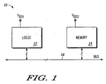
- FIG. 1 illustrates, in block diagram form, an integrated circuit 10 in accordance with an embodiment of the present invention.
- the integrated circuit 10 includes logic circuits 12 and a memory 14.
- the logic circuits 12 may include any type of digital circuit, such as for example, a data processor, an ASIC (application specific integrated circuit), or the like.
- the integrated circuit 10 can be characterized as being a data processing system having an embedded memory.
- the memory 14 is coupled to the logic circuit 14 via a bus 16 and can be any kind of volatile or non-volatile memory.
- memory 14 is a static random access memory (SRAM).
- memory 14 may be a dynamic random access memory (DRAM), a magnetoresistive random access memory (MRAM), ferro-electric random access memory (FeRAM), flash, electrically erasable programmable read only memory (EEPROM), and the like.
- the logic circuits 12 may be coupled directly to the memory 14 instead of via the bus 16.
- the integrated circuit 10 may be a stand-alone memory where the logic circuits 12 are the peripheral circuitry for accessing the memory.
- the logic circuits 12 are coupled to a power supply voltage terminal labeled "VDD1" and the memory 14 is coupled to a power supply voltage terminal labeled "VDD2".
- VDD1 and VDD2 receive positive power supply voltages with respect to ground and are supplied separately.
- power supply voltage VDD1 may, or may not, be equal to VDD2.
- the illustrated embodiment shows two independent power supply voltages. In other embodiments, there may be more than two power supply voltages. Also, in other embodiments, there may be only one power supply voltage. In addition, the power supply voltages may be negative with respect to ground in other embodiments.
- FIG. 2 illustrates, in block diagram form, a portion of the integrated circuit 10 of FIG. 1 .
- FIG. 2 includes the memory 14, a ring oscillator 20, a shift register 22, a register 24, a compare logic circuit 26, and a control circuit 28.
- the memory 14 includes a memory array 30, a row decoder 34, and column logic 36.
- the memory array 30 is a conventional SRAM array and includes a plurality of SRAM cells coupled to bit line pairs and to word lines.
- the memory array 14 may also have the memory cells organized into multiple blocks of memory cells (not shown).
- the memory array 30 includes a "dummy path" for duplicating a worst case critical timing path for a memory access.
- a dummy path may be implemented as part of the memory or as a separate circuit having elements for copying each of the delays in the memory.
- the dummy path is also implemented to track any changes in process and/or temperature in the same way as the memory 14.
- the dummy path is represented by a dummy memory cell 32 coupled to a dummy word line (DWL) and to a dummy bit line pair (DBL/DBL*).
- DWL dummy word line
- DBL/DBL* dummy bit line pair
- the asterisk (*) is used to represent that the dummy bit line DBL* is the logical complement of the dummy bit line DBL.
- the dummy bit lines, dummy word lines, and the dummy memory cell are identical to the actual bit lines, word lines and memory cells of memory array 30.
- the memory 14 has an input for receiving a clock signal labeled "CLK”, an input for receiving a plurality of address signals labeled "ROW ADDRESS” and “COLUMN ADDRESS”, an input for receiving a memory enable signal labeled "MEM EN”, and an input for receiving a read/write signal labeled "R/W”.
- the column logic 36 receives the signals COLUMN ADDRESS and includes column decoders and sense amplifiers for sensing and amplifying the relatively small bit line voltages.
- the memory array 30 is coupled to the power supply voltage terminal VDD2 and to a power supply voltage terminal labeled "VSS".
- VDD2 is for receiving a power supply voltage of about 1.2 volts and VSS is coupled to ground.
- a plurality of bi-directional terminals is used for transmitting data signals DATA to and from the memory 14.
- the memory 14 operates as a conventional embedded RAM.
- the memory enable signal MEM EN is asserted to start an access to memory 14.
- the read/write signal R/W determines whether the access is a read access or a write access.
- a row address is provided to select a word line and a column address is provided to select a bit line pair. Note that in some embodiments, there may be only a single bit line coupled to a column of memory cells instead of a pair.
- a memory cell coupled to the selected word line and bit line pair is accessed for a read or write operation depending on the state of read/write signal R/W. In the case of a write cycle, a data bit is transmitted to the bit line pair via the column logic 36 and stored in the memory cell.
- a data bit is provided by the memory cell to the selected bit line pair and output from the memory via the column logic 36 as data signals DATA.
- the data signals DATA may be provided to, for example, the bus 16 of FIG. 1 for use by logic circuits 12.
- a data processor may provide the control, data, and address signals that are provided to the memory 14.
- Ring oscillator 20 is a conventional ring oscillator having a plurality of inverters coupled in a feedback path and is coupled to a power supply voltage terminal labeled "VDD1" and to a power supply voltage terminal labeled "VSS".
- the ring oscillator 20 provides a clock signal labeled "SHIFT CLK” that varies in response to changes in power supply voltage, process, and temperature.
- the clock signal is provided to a clock input of the shift register 22.
- the ring oscillator 20 tracks process, temperature, and power supply variations in the same manner as the logic circuits 12, and the power supply voltage provided to ring oscillator 20 is the same as the power supply voltage provided to logic circuits 12.
- the power supply voltage provided to VDD1 may be the same as the voltage provided to VDD2 or may be different.
- the shift register 22 is a conventional shift register having a plurality of stages coupled together in series. The number of stages is dependent upon the number of inverters in the ring oscillator 20 and the speed of the logic circuits 12 and memory 14.
- the shift register 22 is enabled by a control signal labeled "SR EN" from the control circuit 28.
- the control circuit 28 receives the memory enable signal MEM EN, the read/write signal R/W, and a signal representing the operating state of the memory labeled "MEM BUSY".
- the control signal SR EN enables the shift register 22 to begin a shifting operation in response to the start of a read access of the memory 14.
- the shift register 22 shifts, for example, a logic one from an input stage toward the output stage in response to the clock signal SHIFT CLK.
- the control signal SR EN causes the shift register 22 to end a shifting operation.
- the number of stages that contain a logic one is compared against a predetermined value, or threshold, stored in the register 24. More specifically, the compare logic 26 has an input for receiving the output from the shift register 22 labeled "SR OUTPUT" and an input for receiving the predetermined value labeled "TH" from the register 24.
- the value TH represents the desired operating speed of the memory.
- the compare logic 26 compares the value SR OUTPUT to the value TH and provides one of a memory slow signal labeled "MEM SLOW" and a memory fast signal labeled "MEM FAST".
- the MEM SLOW signal indicates that the memory is slower than the desired operating speed of the memory.
- the operating speed of the memory may be increased by, for example, increasing the power supply voltage to the power supply voltage terminal VDD2 to the memory.
- the MEM FAST signal indicates that the memory is operating faster than the desired operating speed of the memory. If the MEM FAST signal is provided, the power supply voltage provided to VDD2 may be decreased to conserve power consumption of the integrated circuit 10.
- the desired operating speed of the memory 14 is relative to the speed of the logic circuits 12 as determined by the speed of the ring oscillator 20. Note that in other embodiments, there may be more than one predetermined threshold voltage TH to compare against the signal SR OUTPUT.
- the shift register 22 is cleared upon completion of the comparison step. Also, the shift register 22 may be cleared when and if the integrated circuit 10 is cleared. For the purposes of clarity and simplicity, the means for resetting or clearing the shift register 22 is not shown but is well known in the art. Also, in other embodiments, the shift register 22 may be replaced with a counter that outputs a count value to compare with the threshold TH.
- FIG. 3 illustrates several possible comparison results for the compare logic of FIG. 2 .
- shift register 22 is shown having 8 bits for illustration purposes. In an actual embodiment, shifter register 22 may have, for example, 32 or 64 bits. The mid point of the shift register 22 is marked with "TH", indicating the bit position for the desired memory operating speed in the illustrated embodiment. In other embodiments, the desired memory operating speed may coincide with another bit position of shift register 22.
- a logic one is shifted into the left side of shift register 22 in response to a memory read operation being started as indicated by control signal SR EN being asserted.
- the logic one has been shifted to the fourth bit position. Because the SR output is equal to value TH, the output signal MEM SLOW is zero and the output signal MEM FAST is zero, indicating that the memory is operating at the desired speed and therefore the power supply voltage VDD2 provided to the memory 14 is optimal.
- a logic one is shifted into the left side of shift register 22 in response to a memory read operation being started as indicated by control signal SR EN being asserted. At the end of the read operation, the logic one has been shifted to the second bit position.
- the SR OUTPUT is less than the value TH, indicating that the memory is faster than desired.
- the compare logic 26 outputs a logic zero MEM SLOW and a logic one MEM FAST.
- a system that includes memory 14 may cause an interrupt to be generated and the power supply voltage to memory 14 to be lowered by a predetermined amount. On the next memory read access, the speed will be checked again and another incremental adjustment to VDD2 will be made if necessary.
- An example 39 illustrates a case where the SR OUTPUT is higher than the value TH.
- the logic one has been shifted to the sixth bit position.
- the compare logic 26 will output a logic one MEM SLOW and a logic zero MEM FAST.
- An interrupt may be generated in the integrated circuit 10 and the power supply voltage VDD2 adjusted higher to increase the speed of the memory operations. On the next and subsequent read operations, the speed will be checked and other adjustments made to the power supply voltage VDD2 if necessary.
- FIG. 4 illustrates a method for changing an operating parameter of the integrated circuit of FIG. 1 .
- the operating parameter is the power supply voltage to the memory.
- the operating parameter may be another user-controlled or environment variable for the memory.
- a "user" can be a human operator or another portion of a system that includes integrated circuit 10.
- an access to the memory is begun and a worst case critical path for the access is timed using the dummy path in the memory.
- a portion of the dummy path includes the dummy word line DWL and the dummy bit line pair DBL/DBL as illustrated in FIG. 2 .
- Other portions of the dummy path are not illustrated but would be included in other parts of the memory that affect the access time of the memory.
- the shift register 22 is enabled in response to the read access by an asserted control signal SR EN.
- the end of the read access is detected by the control logic 28 receiving a deasserted MEM BUSY signal.
- the control signal SR EN is deasserted causing the shift register 22 to stop shifting.
- the shift register output SR OUTPUT is provided as an input to the compare logic 26.
- the state of the shift register 22 is compared with a value representing the desired operating speed of the memory. The state of shift register 22 is determined by how many stages across the shift register a bit is shifted as discussed above in reference to FIG. 3 . Also, the shift register 22 is cleared by a reset signal (not shown) as discussed above.
- step 48 an operating parameter of the memory is changed in response to the comparison of step 46.
- the power supply voltage VDD2 may be reduced to slow down the memory and conserve power.
- the power supply voltage VDD2 is raised to increase the speed of the memory.
Description
- The present invention relates generally to integrated circuits, and more particularly, to an apparatus and method for adjusting an operating parameter of an integrated circuit.
- Generally, it is desirable for an integrated circuit to operate with the lowest possible power consumption. One way to reduce power consumption is to lower the power supply voltage to the integrated circuit. Also, it is desirable to operate the integrated circuit at the lowest power supply voltage under all process and temperature changes. However, lowering the power supply voltage reduces the switching speed of the transistors of the integrated circuit. Also, in an integrated circuit that has both memory cells and logic circuits, the rate of change in access time of memory circuits may be different than the rate of change in switching speed of logic circuits. In some systems, such as the system described in
U.S. Patent Publication Number 2005/0283630 A1 , a determination may be made whether a core is likely to properly operate when a power supply to a processor that includes the core is altered." Therefore, in order to compensate for temperature and process changes in an integrated circuit having both memory cells and logic circuits, it would be useful to be able to determine the relative difference in induced speed variations caused by the power supply voltage, temperature and process changes for both memory cells and logic circuits. - The invention provides a method according to
claim 1 and an apparatus according to claim 8. - The present invention is illustrated by way of example and not limited by the accompanying figures, in which like references indicate similar elements, and in which:
-
FIG. 1 illustrates, in block diagram form, an integrated circuit in accordance with an embodiment of the present invention. -
FIG. 2 illustrates, in block diagram form, a portion of the integrated circuit ofFIG. 1 . -
FIG. 3 illustrates several comparison results for the compare logic ofFIG. 2 . -
FIG. 4 illustrates a method for changing an operating parameter of the integrated circuit ofFIG. 1 . - Skilled artisans appreciate that elements in the figures are illustrated for simplicity and clarity and have not necessarily been drawn to scale. For example, the dimensions of some of the elements in the figures may be exaggerated relative to other elements to help improve the understanding of the embodiments of the present invention.
- As used herein, the term "bus" is used to refer to a plurality of signals or conductors which may be used to transfer one or more various types of information, such as data, addresses, control, or status. The conductors as discussed herein may be illustrated or described in reference to being a single conductor, a plurality of conductors, unidirectional conductors, or bidirectional conductors. However, different embodiments may vary the implementation of the conductors. For example, separate unidirectional conductors may be used rather than bidirectional conductors and vice versa. Also, the plurality of conductors may be replaced with a single conductor that transfers multiple signals serially or in a time multiplexed manner. Likewise, single conductors carrying multiple signals may be separated out into various different conductors carrying subsets of these signals. Therefore, many options exist for transferring signals.
- Generally, the present invention provides an apparatus and method for adjusting an operating parameter of an integrated circuit having both a logic circuit and a memory. In the illustrated embodiment, the operating parameter to be adjusted is the power supply voltage to a memory on the integrated circuit. In another embodiment the operating parameter may be a clock frequency of the integrated circuit or an element of the integrated circuit environment, such as for example, temperature. The apparatus includes a ring oscillator, a shift register and compare logic. The ring oscillator provides a clock signal that is dependent on the ring oscillator's power supply voltage, temperature, and process. The clock signal is used to clock a shift register. The shift register begins a shifting operation in response to a read access to the memory. The shifting operation is terminated in response to completing the read access. The number of shifting operations is then compared to a predetermined value, where the predetermined value represents a desired operating speed of the memory. If the number of shifting operations is greater than the predetermined value, then the memory is slower than desired, and if the number of shifting operations is less than the predetermined value, then the memory is faster than desired. The power supply voltage can be adjusted to change the operating speed of the memory based on the comparison. In the illustrated embodiment, the speed of the memory is determined using a dummy path representing the worst case access time for the memory.
- The disclosed embodiment provides a way to track the difference between logic performance and memory performance against changes in process, temperature, and voltage dynamically, in real time. The power supply voltages for the integrated circuit can then be adjusted for optimal performance of both the memory and the logic circuits.
-
FIG. 1 illustrates, in block diagram form, anintegrated circuit 10 in accordance with an embodiment of the present invention. Theintegrated circuit 10 includeslogic circuits 12 and amemory 14. Thelogic circuits 12 may include any type of digital circuit, such as for example, a data processor, an ASIC (application specific integrated circuit), or the like. In the illustrated embodiment, the integratedcircuit 10 can be characterized as being a data processing system having an embedded memory. Thememory 14 is coupled to thelogic circuit 14 via abus 16 and can be any kind of volatile or non-volatile memory. In the illustrated embodiment,memory 14 is a static random access memory (SRAM). In another embodiment,memory 14 may be a dynamic random access memory (DRAM), a magnetoresistive random access memory (MRAM), ferro-electric random access memory (FeRAM), flash, electrically erasable programmable read only memory (EEPROM), and the like. Also, thelogic circuits 12 may be coupled directly to thememory 14 instead of via thebus 16. Also, theintegrated circuit 10 may be a stand-alone memory where thelogic circuits 12 are the peripheral circuitry for accessing the memory. - The
logic circuits 12 are coupled to a power supply voltage terminal labeled "VDD1" and thememory 14 is coupled to a power supply voltage terminal labeled "VDD2". In the illustrated embodiment, VDD1 and VDD2 receive positive power supply voltages with respect to ground and are supplied separately. Also, power supply voltage VDD1 may, or may not, be equal to VDD2. Note that the illustrated embodiment shows two independent power supply voltages. In other embodiments, there may be more than two power supply voltages. Also, in other embodiments, there may be only one power supply voltage. In addition, the power supply voltages may be negative with respect to ground in other embodiments. -
FIG. 2 illustrates, in block diagram form, a portion of theintegrated circuit 10 ofFIG. 1 .FIG. 2 includes thememory 14, aring oscillator 20, ashift register 22, aregister 24, acompare logic circuit 26, and acontrol circuit 28. Thememory 14 includes amemory array 30, arow decoder 34, andcolumn logic 36. Thememory array 30 is a conventional SRAM array and includes a plurality of SRAM cells coupled to bit line pairs and to word lines. Thememory array 14 may also have the memory cells organized into multiple blocks of memory cells (not shown). In addition, thememory array 30 includes a "dummy path" for duplicating a worst case critical timing path for a memory access. A dummy path may be implemented as part of the memory or as a separate circuit having elements for copying each of the delays in the memory. The dummy path is also implemented to track any changes in process and/or temperature in the same way as thememory 14. In the illustrated embodiment, the dummy path is represented by adummy memory cell 32 coupled to a dummy word line (DWL) and to a dummy bit line pair (DBL/DBL*). Note that the asterisk (*) is used to represent that the dummy bit line DBL* is the logical complement of the dummy bit line DBL. The dummy bit lines, dummy word lines, and the dummy memory cell are identical to the actual bit lines, word lines and memory cells ofmemory array 30. Thememory 14 has an input for receiving a clock signal labeled "CLK", an input for receiving a plurality of address signals labeled "ROW ADDRESS" and "COLUMN ADDRESS", an input for receiving a memory enable signal labeled "MEM EN", and an input for receiving a read/write signal labeled "R/W". Thecolumn logic 36 receives the signals COLUMN ADDRESS and includes column decoders and sense amplifiers for sensing and amplifying the relatively small bit line voltages. In addition, thememory array 30 is coupled to the power supply voltage terminal VDD2 and to a power supply voltage terminal labeled "VSS". In the illustrated embodiment, VDD2 is for receiving a power supply voltage of about 1.2 volts and VSS is coupled to ground. A plurality of bi-directional terminals is used for transmitting data signals DATA to and from thememory 14. - The
memory 14 operates as a conventional embedded RAM. The memory enable signal MEM EN is asserted to start an access tomemory 14. The read/write signal R/W determines whether the access is a read access or a write access. A row address is provided to select a word line and a column address is provided to select a bit line pair. Note that in some embodiments, there may be only a single bit line coupled to a column of memory cells instead of a pair. A memory cell coupled to the selected word line and bit line pair is accessed for a read or write operation depending on the state of read/write signal R/W. In the case of a write cycle, a data bit is transmitted to the bit line pair via thecolumn logic 36 and stored in the memory cell. In the case of a read cycle, a data bit is provided by the memory cell to the selected bit line pair and output from the memory via thecolumn logic 36 as data signals DATA. The data signals DATA may be provided to, for example, thebus 16 ofFIG. 1 for use bylogic circuits 12. A data processor may provide the control, data, and address signals that are provided to thememory 14. -
Ring oscillator 20 is a conventional ring oscillator having a plurality of inverters coupled in a feedback path and is coupled to a power supply voltage terminal labeled "VDD1" and to a power supply voltage terminal labeled "VSS". Thering oscillator 20 provides a clock signal labeled "SHIFT CLK" that varies in response to changes in power supply voltage, process, and temperature. The clock signal is provided to a clock input of theshift register 22. Thering oscillator 20 tracks process, temperature, and power supply variations in the same manner as thelogic circuits 12, and the power supply voltage provided toring oscillator 20 is the same as the power supply voltage provided tologic circuits 12. Also note that the power supply voltage provided to VDD1 may be the same as the voltage provided to VDD2 or may be different. - The
shift register 22 is a conventional shift register having a plurality of stages coupled together in series. The number of stages is dependent upon the number of inverters in thering oscillator 20 and the speed of thelogic circuits 12 andmemory 14. Theshift register 22 is enabled by a control signal labeled "SR EN" from thecontrol circuit 28. Thecontrol circuit 28 receives the memory enable signal MEM EN, the read/write signal R/W, and a signal representing the operating state of the memory labeled "MEM BUSY". The control signal SR EN enables theshift register 22 to begin a shifting operation in response to the start of a read access of thememory 14. Theshift register 22 shifts, for example, a logic one from an input stage toward the output stage in response to the clock signal SHIFT CLK. At the end of a memory operation the control signal SR EN causes theshift register 22 to end a shifting operation. At the end of the shifting operation the number of stages that contain a logic one is compared against a predetermined value, or threshold, stored in theregister 24. More specifically, the comparelogic 26 has an input for receiving the output from theshift register 22 labeled "SR OUTPUT" and an input for receiving the predetermined value labeled "TH" from theregister 24. The value TH represents the desired operating speed of the memory. The comparelogic 26 compares the value SR OUTPUT to the value TH and provides one of a memory slow signal labeled "MEM SLOW" and a memory fast signal labeled "MEM FAST". The MEM SLOW signal indicates that the memory is slower than the desired operating speed of the memory. The operating speed of the memory may be increased by, for example, increasing the power supply voltage to the power supply voltage terminal VDD2 to the memory. On the other hand, the MEM FAST signal indicates that the memory is operating faster than the desired operating speed of the memory. If the MEM FAST signal is provided, the power supply voltage provided to VDD2 may be decreased to conserve power consumption of theintegrated circuit 10. In the illustrated embodiment, the desired operating speed of thememory 14 is relative to the speed of thelogic circuits 12 as determined by the speed of thering oscillator 20. Note that in other embodiments, there may be more than one predetermined threshold voltage TH to compare against the signal SR OUTPUT. - The
shift register 22 is cleared upon completion of the comparison step. Also, theshift register 22 may be cleared when and if theintegrated circuit 10 is cleared. For the purposes of clarity and simplicity, the means for resetting or clearing theshift register 22 is not shown but is well known in the art. Also, in other embodiments, theshift register 22 may be replaced with a counter that outputs a count value to compare with the threshold TH. -
FIG. 3 illustrates several possible comparison results for the compare logic ofFIG. 2 . InFIG. 3 ,shift register 22 is shown having 8 bits for illustration purposes. In an actual embodiment, shifter register 22 may have, for example, 32 or 64 bits. The mid point of theshift register 22 is marked with "TH", indicating the bit position for the desired memory operating speed in the illustrated embodiment. In other embodiments, the desired memory operating speed may coincide with another bit position ofshift register 22. - In an example 37, a logic one is shifted into the left side of
shift register 22 in response to a memory read operation being started as indicated by control signal SR EN being asserted. At the end of the read operation, as indicated by the control signal SR EN being deasserted, the logic one has been shifted to the fourth bit position. Because the SR output is equal to value TH, the output signal MEM SLOW is zero and the output signal MEM FAST is zero, indicating that the memory is operating at the desired speed and therefore the power supply voltage VDD2 provided to thememory 14 is optimal. - In an example 38, a logic one is shifted into the left side of
shift register 22 in response to a memory read operation being started as indicated by control signal SR EN being asserted. At the end of the read operation, the logic one has been shifted to the second bit position. The SR OUTPUT is less than the value TH, indicating that the memory is faster than desired. The comparelogic 26 outputs a logic zero MEM SLOW and a logic one MEM FAST. In response to the comparison output, a system that includesmemory 14 may cause an interrupt to be generated and the power supply voltage tomemory 14 to be lowered by a predetermined amount. On the next memory read access, the speed will be checked again and another incremental adjustment to VDD2 will be made if necessary. - An example 39 illustrates a case where the SR OUTPUT is higher than the value TH. At the end of the read operation, the logic one has been shifted to the sixth bit position. The compare
logic 26 will output a logic one MEM SLOW and a logic zero MEM FAST. An interrupt may be generated in theintegrated circuit 10 and the power supply voltage VDD2 adjusted higher to increase the speed of the memory operations. On the next and subsequent read operations, the speed will be checked and other adjustments made to the power supply voltage VDD2 if necessary. -
FIG. 4 illustrates a method for changing an operating parameter of the integrated circuit ofFIG. 1 . In the illustrated embodiment, the operating parameter is the power supply voltage to the memory. In other embodiments, the operating parameter may be another user-controlled or environment variable for the memory. In the illustrated embodiment, a "user" can be a human operator or another portion of a system that includes integratedcircuit 10. Atstep 40, an access to the memory is begun and a worst case critical path for the access is timed using the dummy path in the memory. A portion of the dummy path includes the dummy word line DWL and the dummy bit line pair DBL/DBL as illustrated inFIG. 2 . Other portions of the dummy path are not illustrated but would be included in other parts of the memory that affect the access time of the memory. Atstep 42, theshift register 22 is enabled in response to the read access by an asserted control signal SR EN. Atstep 44, the end of the read access is detected by thecontrol logic 28 receiving a deasserted MEM BUSY signal. The control signal SR EN is deasserted causing theshift register 22 to stop shifting. The shift register output SR OUTPUT is provided as an input to the comparelogic 26. Atstep 46, the state of theshift register 22 is compared with a value representing the desired operating speed of the memory. The state ofshift register 22 is determined by how many stages across the shift register a bit is shifted as discussed above in reference toFIG. 3 . Also, theshift register 22 is cleared by a reset signal (not shown) as discussed above. If the number of shifted bits is greater than the threshold TH, then the memory is slower than desired. If the number of shifted bits is less than the threshold TH, the memory is faster than desired. Atstep 48, an operating parameter of the memory is changed in response to the comparison ofstep 46. In the case where the number of shifted bits is less than the threshold TH, the power supply voltage VDD2 may be reduced to slow down the memory and conserve power. In the case where the number of shifted bits is greater than the threshold TH, the power supply voltage VDD2 is raised to increase the speed of the memory. - In the foregoing specification, the invention has been described with reference to specific embodiments. However, one of ordinary skill in the art appreciates that various modifications and changes can be made without departing from the scope of the present invention as set forth in the claims below. Accordingly, the specification and figures are to be regarded in an illustrative rather than a restrictive sense, and all such modifications are intended to be included within the scope of the present invention as defined by the independent claims.
Claims (11)
- A method for adjusting an operating parameter of a data processing system (10) having a memory (14) and logic (12), the logic coupled to the memory and comprising a timing circuit (20, 22, 26), the method characterized comprising:initiating (40) a memory access, wherein a speed of the memory access is affected by a first operating parameter provided to the memory;in response to the initiating, enabling (42) counting circuitry (22) to count pulses generated by the timing circuit, wherein a speed of the timing circuit is affected by a second operating parameter provided to the timing circuit, and the second operating parameter is independent of the first operating parameter;in response to completing (44) the memory access, the counting circuitry outputting a count value;using the count value to determine (46) a relative speed of the memory access with respect to the speed of the timing circuit; andbased on the relative speed, adjusting (48) the speed of the memory by adjusting the first operating parameter of the data processing system (10).
- The method of claim 1, wherein the relative speed indicates whether an operating speed of the memory (14) is faster, slower, or equal to an operating speed of the logic (12).
- The method of claim 1, wherein the timing circuitry (20) comprises a ring oscillator, and wherein the relative speed of the memory access is relative to a frequency of the ring oscillator.
- The method of claim 3, wherein the counting circuitry (22) comprises a shift register clocked by the ring oscillator (20), and wherein the enabling the counting circuitry comprises enabling the shift register.
- The method of claim 1, wherein the memory access comprises an access to a dummy path (30) of the memory (14).
- The method of claim 1, wherein the using the count value to determine the relative speed comprises comparing the count value to a threshold value.
- The method of claim 6, wherein the threshold value represents a desired value of an operating speed of the memory (14).
- An integrated circuit comprising a data processing system (10), the data processing system comprising:a memory (14), wherein a speed of the memory is affected by a first operating parameter provided to the memory; andlogic (12) comprising a timing circuit (20, 22, 26), wherein a speed of the timing circuit is affected by a second operating parameter that is independent of the first operating parameter, andwherein the timing circuit includes:a ring oscillator (20);a shift register (22) having a clock input coupled to an output of the ring oscillator (20), the shift register being enabled in response to initiating a memory access to the memory (14) and disabled in response to completing the memory access; andcompare logic (26) coupled to an output of the shift register and providing a relative speed indicator representative of a relative speed of the memory with respect to the timing circuit, wherein the speed of the memory is adjusted by adjusting the first operating parameter of the data processing system based on the relative speed indicator.
- The integrated circuit of claim 8, wherein a data input of the shift register (22) is coupled to a fixed voltage representative of a known logic state.
- The integrated circuit of claim 8, wherein the compare logic (26) compares the output of the shift register (22) with a threshold value to provide the relative speed indicator.
- The integrated circuit of claim 8, wherein the relative speed indicator is representative of the relative speed of the memory to a frequency of the ring oscillator (20).
Applications Claiming Priority (2)
| Application Number | Priority Date | Filing Date | Title |
|---|---|---|---|
| US11/366,286 US7483327B2 (en) | 2006-03-02 | 2006-03-02 | Apparatus and method for adjusting an operating parameter of an integrated circuit |
| PCT/US2007/061189 WO2007117745A2 (en) | 2006-03-02 | 2007-01-29 | Apparatus and method for adjusting an operating parameter of an integrated circuit |
Publications (3)
| Publication Number | Publication Date |
|---|---|
| EP1994420A2 EP1994420A2 (en) | 2008-11-26 |
| EP1994420A4 EP1994420A4 (en) | 2013-06-05 |
| EP1994420B1 true EP1994420B1 (en) | 2016-09-28 |
Family
ID=38519422
Family Applications (1)
| Application Number | Title | Priority Date | Filing Date |
|---|---|---|---|
| EP07756489.6A Active EP1994420B1 (en) | 2006-03-02 | 2007-01-29 | Apparatus and method for adjusting an operating parameter of an integrated circuit |
Country Status (6)
| Country | Link |
|---|---|
| US (1) | US7483327B2 (en) |
| EP (1) | EP1994420B1 (en) |
| JP (1) | JP4932856B2 (en) |
| KR (1) | KR101367063B1 (en) |
| TW (1) | TWI459403B (en) |
| WO (1) | WO2007117745A2 (en) |
Families Citing this family (29)
| Publication number | Priority date | Publication date | Assignee | Title |
|---|---|---|---|---|
| US7639542B2 (en) * | 2006-05-15 | 2009-12-29 | Apple Inc. | Maintenance operations for multi-level data storage cells |
| US7511646B2 (en) * | 2006-05-15 | 2009-03-31 | Apple Inc. | Use of 8-bit or higher A/D for NAND cell value |
| US8000134B2 (en) * | 2006-05-15 | 2011-08-16 | Apple Inc. | Off-die charge pump that supplies multiple flash devices |
| US7852690B2 (en) * | 2006-05-15 | 2010-12-14 | Apple Inc. | Multi-chip package for a flash memory |
| US7613043B2 (en) * | 2006-05-15 | 2009-11-03 | Apple Inc. | Shifting reference values to account for voltage sag |
| US7551486B2 (en) * | 2006-05-15 | 2009-06-23 | Apple Inc. | Iterative memory cell charging based on reference cell value |
| US7568135B2 (en) | 2006-05-15 | 2009-07-28 | Apple Inc. | Use of alternative value in cell detection |
| US7701797B2 (en) * | 2006-05-15 | 2010-04-20 | Apple Inc. | Two levels of voltage regulation supplied for logic and data programming voltage of a memory device |
| US7911834B2 (en) * | 2006-05-15 | 2011-03-22 | Apple Inc. | Analog interface for a flash memory die |
| US7639531B2 (en) * | 2006-05-15 | 2009-12-29 | Apple Inc. | Dynamic cell bit resolution |
| US7546410B2 (en) * | 2006-07-26 | 2009-06-09 | International Business Machines Corporation | Self timed memory chip having an apportionable data bus |
| US8050781B2 (en) * | 2007-06-29 | 2011-11-01 | Emulex Design & Manufacturing Corporation | Systems and methods for ASIC power consumption reduction |
| JP5228468B2 (en) * | 2007-12-17 | 2013-07-03 | 富士通セミコンダクター株式会社 | System device and method of operating system device |
| US7684263B2 (en) * | 2008-01-17 | 2010-03-23 | International Business Machines Corporation | Method and circuit for implementing enhanced SRAM write and read performance ring oscillator |
| US7852692B2 (en) * | 2008-06-30 | 2010-12-14 | Freescale Semiconductor, Inc. | Memory operation testing |
| US8909957B2 (en) * | 2010-11-04 | 2014-12-09 | Lenovo Enterprise Solutions (Singapore) Pte. Ltd. | Dynamic voltage adjustment to computer system memory |
| KR20130021175A (en) | 2011-08-22 | 2013-03-05 | 삼성전자주식회사 | Memory device and devices having the same |
| US8717831B2 (en) | 2012-04-30 | 2014-05-06 | Hewlett-Packard Development Company, L.P. | Memory circuit |
| US9105328B2 (en) | 2012-07-31 | 2015-08-11 | Taiwan Semiconductor Manufacturing Company, Ltd. | Tracking signals in memory write or read operation |
| CN104838445A (en) * | 2012-12-11 | 2015-08-12 | 惠普发展公司,有限责任合伙企业 | Data operation in shift register ring |
| JP2016514338A (en) | 2013-03-28 | 2016-05-19 | ヒューレット−パッカード デベロップメント カンパニー エル.ピー.Hewlett‐Packard Development Company, L.P. | Storage device reading apparatus and method |
| KR20150043122A (en) * | 2013-10-14 | 2015-04-22 | 에스케이하이닉스 주식회사 | Semiconductor device |
| US9858217B1 (en) * | 2016-06-29 | 2018-01-02 | Qualcomm Incorporated | Within-die special oscillator for tracking SRAM memory performance with global process variation, voltage and temperature |
| US11196574B2 (en) | 2017-08-17 | 2021-12-07 | Taiwan Semiconductor Manufacturing Company, Ltd. | Physically unclonable function (PUF) generation |
| US11294678B2 (en) | 2018-05-29 | 2022-04-05 | Advanced Micro Devices, Inc. | Scheduler queue assignment |
| US11334384B2 (en) * | 2019-12-10 | 2022-05-17 | Advanced Micro Devices, Inc. | Scheduler queue assignment burst mode |
| KR20220022618A (en) | 2020-08-19 | 2022-02-28 | 에스케이하이닉스 주식회사 | Clock monotoring circuit |
| US11948000B2 (en) | 2020-10-27 | 2024-04-02 | Advanced Micro Devices, Inc. | Gang scheduling for low-latency task synchronization |
| CN114705973B (en) * | 2022-06-01 | 2022-11-11 | 北京航空航天大学杭州创新研究院 | Non-invasive complex environment integrated circuit aging monitoring method |
Family Cites Families (16)
| Publication number | Priority date | Publication date | Assignee | Title |
|---|---|---|---|---|
| US4326269A (en) * | 1980-06-09 | 1982-04-20 | General Electric Company | One bit memory for bipolar signals |
| JPH04190389A (en) * | 1990-11-26 | 1992-07-08 | Hitachi Ltd | Look-up table rewriting system for image display device |
| JP3609868B2 (en) | 1995-05-30 | 2005-01-12 | 株式会社ルネサステクノロジ | Static semiconductor memory device |
| US5978929A (en) * | 1997-03-20 | 1999-11-02 | International Business Machines Corporation | Computer unit responsive to difference between external clock period and circuit characteristic period |
| JP2001034530A (en) * | 1999-07-16 | 2001-02-09 | Mitsubishi Electric Corp | Microcomputer and memory access control method |
| US6327224B1 (en) | 2000-06-16 | 2001-12-04 | International Business Machines Corporation | On-chip method for measuring access time and data-pin spread |
| US6269043B1 (en) * | 2000-07-31 | 2001-07-31 | Cisco Technology, Inc. | Power conservation system employing a snooze mode |
| JP2002244917A (en) * | 2001-02-15 | 2002-08-30 | Matsushita Electric Ind Co Ltd | Access management device and program |
| US6483754B1 (en) | 2001-05-16 | 2002-11-19 | Lsi Logic Corporation | Self-time scheme to reduce cycle time for memories |
| JP4894095B2 (en) * | 2001-06-15 | 2012-03-07 | 富士通セミコンダクター株式会社 | Semiconductor memory device |
| US6901027B2 (en) * | 2002-04-30 | 2005-05-31 | Sony Corporation | Apparatus for processing data, memory bank used therefor, semiconductor device, and method for reading out pixel data |
| US6985375B2 (en) * | 2003-06-11 | 2006-01-10 | Micron Technology, Inc. | Adjusting the frequency of an oscillator for use in a resistive sense amp |
| JP4025260B2 (en) * | 2003-08-14 | 2007-12-19 | 株式会社東芝 | Scheduling method and information processing system |
| JP4198644B2 (en) | 2004-06-21 | 2008-12-17 | 富士通マイクロエレクトロニクス株式会社 | Semiconductor integrated circuit |
| US7409315B2 (en) | 2004-06-28 | 2008-08-05 | Broadcom Corporation | On-board performance monitor and power control system |
| US7327185B2 (en) * | 2004-11-02 | 2008-02-05 | Texas Instruments Incorporated | Selectable application of offset to dynamically controlled voltage supply |
-
2006
- 2006-03-02 US US11/366,286 patent/US7483327B2/en active Active
-
2007
- 2007-01-29 KR KR1020087024174A patent/KR101367063B1/en active IP Right Grant
- 2007-01-29 WO PCT/US2007/061189 patent/WO2007117745A2/en active Application Filing
- 2007-01-29 JP JP2008557438A patent/JP4932856B2/en active Active
- 2007-01-29 EP EP07756489.6A patent/EP1994420B1/en active Active
- 2007-02-13 TW TW096105319A patent/TWI459403B/en active
Also Published As
| Publication number | Publication date |
|---|---|
| TWI459403B (en) | 2014-11-01 |
| JP4932856B2 (en) | 2012-05-16 |
| WO2007117745A2 (en) | 2007-10-18 |
| US7483327B2 (en) | 2009-01-27 |
| US20070220388A1 (en) | 2007-09-20 |
| KR20080100474A (en) | 2008-11-18 |
| KR101367063B1 (en) | 2014-02-24 |
| WO2007117745A3 (en) | 2008-05-22 |
| JP2009528635A (en) | 2009-08-06 |
| TW200739604A (en) | 2007-10-16 |
| EP1994420A4 (en) | 2013-06-05 |
| EP1994420A2 (en) | 2008-11-26 |
Similar Documents
| Publication | Publication Date | Title |
|---|---|---|
| EP1994420B1 (en) | Apparatus and method for adjusting an operating parameter of an integrated circuit | |
| US11901037B2 (en) | Apparatuses and methods for storing and writing multiple parameter codes for memory operating parameters | |
| US5909125A (en) | FPGA using RAM control signal lines as routing or logic resources after configuration | |
| US7266009B2 (en) | Ferroelectric memory | |
| US7474553B2 (en) | Device writing to a plurality of rows in a memory matrix simultaneously | |
| CN104375970A (en) | Semiconductor integrated circuit | |
| US6999367B2 (en) | Semiconductor memory device | |
| JP3754593B2 (en) | Integrated circuit having memory cells for storing data bits and method for writing write data bits to memory cells in integrated circuits | |
| EP2026353B1 (en) | AC sensing for a resistive memory | |
| US7054204B2 (en) | Semiconductor device and method for controlling the same | |
| US9478262B2 (en) | Semiconductor device including input/output circuit | |
| US20090323390A1 (en) | Semiconductor memory device | |
| US7603535B2 (en) | Low power consumption semiconductor memory device capable of selectively changing input/output data width and data input/output method | |
| WO2007015097A1 (en) | Memory bitcell and method of using the same | |
| US6337826B1 (en) | Clock synchronization semiconductor memory device sequentially outputting data bit by bit | |
| CN113963728A (en) | Semiconductor device and semiconductor memory device | |
| US7978547B2 (en) | Data I/O control signal generating circuit in a semiconductor memory apparatus | |
| US7606083B2 (en) | Semiconductor memory device with a noise filter and method of controlling the same | |
| US11862291B2 (en) | Integrated counter in memory device | |
| US6304103B1 (en) | FPGA using RAM control signal lines as routing or logic resources after configuration | |
| KR100546136B1 (en) | Nonvolatile Ferroelectric Memory Devices with Wide Page Buffers | |
| US7218564B2 (en) | Dual equalization devices for long data line pairs | |
| CN115954022A (en) | Latch circuit, transmission circuit, and semiconductor device | |
| KR19980047692A (en) | Input buffer circuit | |
| JPH0831192A (en) | Storage device |
Legal Events
| Date | Code | Title | Description |
|---|---|---|---|
| PUAI | Public reference made under article 153(3) epc to a published international application that has entered the european phase |
Free format text: ORIGINAL CODE: 0009012 |
|
| AK | Designated contracting states |
Kind code of ref document: A2 Designated state(s): AT BE BG CH CY CZ DE DK EE ES FI FR GB GR HU IE IS IT LI LT LU LV MC NL PL PT RO SE SI SK TR |
|
| AX | Request for extension of the european patent |
Extension state: AL BA HR MK RS |
|
| 17P | Request for examination filed |
Effective date: 20081124 |
|
| RBV | Designated contracting states (corrected) |
Designated state(s): DE FR GB |
|
| RBV | Designated contracting states (corrected) |
Designated state(s): DE FR GB |
|
| DAX | Request for extension of the european patent (deleted) | ||
| A4 | Supplementary search report drawn up and despatched |
Effective date: 20130507 |
|
| RIC1 | Information provided on ipc code assigned before grant |
Ipc: G01R 31/28 20060101AFI20130430BHEP |
|
| GRAP | Despatch of communication of intention to grant a patent |
Free format text: ORIGINAL CODE: EPIDOSNIGR1 |
|
| INTG | Intention to grant announced |
Effective date: 20151119 |
|
| GRAP | Despatch of communication of intention to grant a patent |
Free format text: ORIGINAL CODE: EPIDOSNIGR1 |
|
| INTG | Intention to grant announced |
Effective date: 20160415 |
|
| GRAS | Grant fee paid |
Free format text: ORIGINAL CODE: EPIDOSNIGR3 |
|
| GRAA | (expected) grant |
Free format text: ORIGINAL CODE: 0009210 |
|
| AK | Designated contracting states |
Kind code of ref document: B1 Designated state(s): DE FR GB |
|
| REG | Reference to a national code |
Ref country code: GB Ref legal event code: FG4D |
|
| REG | Reference to a national code |
Ref country code: DE Ref legal event code: R096 Ref document number: 602007048100 Country of ref document: DE |
|
| RAP2 | Party data changed (patent owner data changed or rights of a patent transferred) |
Owner name: NXP USA, INC. |
|
| REG | Reference to a national code |
Ref country code: FR Ref legal event code: PLFP Year of fee payment: 11 |
|
| REG | Reference to a national code |
Ref country code: DE Ref legal event code: R097 Ref document number: 602007048100 Country of ref document: DE |
|
| PLBE | No opposition filed within time limit |
Free format text: ORIGINAL CODE: 0009261 |
|
| STAA | Information on the status of an ep patent application or granted ep patent |
Free format text: STATUS: NO OPPOSITION FILED WITHIN TIME LIMIT |
|
| 26N | No opposition filed |
Effective date: 20170629 |
|
| REG | Reference to a national code |
Ref country code: GB Ref legal event code: 732E Free format text: REGISTERED BETWEEN 20171116 AND 20171122 |
|
| REG | Reference to a national code |
Ref country code: FR Ref legal event code: PLFP Year of fee payment: 12 |
|
| REG | Reference to a national code |
Ref country code: DE Ref legal event code: R081 Ref document number: 602007048100 Country of ref document: DE Owner name: NXP USA, INC. (N.D.GES.D.STAATES DELAWARE), AU, US Free format text: FORMER OWNER: FREESCALE SEMICONDUCTOR, INC., AUSTIN, TEX., US |
|
| PGFP | Annual fee paid to national office [announced via postgrant information from national office to epo] |
Ref country code: DE Payment date: 20221220 Year of fee payment: 17 |
|
| P01 | Opt-out of the competence of the unified patent court (upc) registered |
Effective date: 20230725 |
|
| PGFP | Annual fee paid to national office [announced via postgrant information from national office to epo] |
Ref country code: GB Payment date: 20231219 Year of fee payment: 18 |
|
| PGFP | Annual fee paid to national office [announced via postgrant information from national office to epo] |
Ref country code: FR Payment date: 20231219 Year of fee payment: 18 |