EP1993138A2 - Device with a strained-channel transistor - Google Patents
Device with a strained-channel transistor Download PDFInfo
- Publication number
- EP1993138A2 EP1993138A2 EP08155761A EP08155761A EP1993138A2 EP 1993138 A2 EP1993138 A2 EP 1993138A2 EP 08155761 A EP08155761 A EP 08155761A EP 08155761 A EP08155761 A EP 08155761A EP 1993138 A2 EP1993138 A2 EP 1993138A2
- Authority
- EP
- European Patent Office
- Prior art keywords
- layer
- gate
- transistor
- piezoelectric
- substrate
- Prior art date
- Legal status (The legal status is an assumption and is not a legal conclusion. Google has not performed a legal analysis and makes no representation as to the accuracy of the status listed.)
- Granted
Links
- 239000004065 semiconductor Substances 0.000 claims abstract description 39
- 230000010287 polarization Effects 0.000 claims abstract description 26
- 238000000034 method Methods 0.000 claims abstract description 23
- 238000004519 manufacturing process Methods 0.000 claims abstract description 13
- 230000001939 inductive effect Effects 0.000 claims abstract description 5
- 230000000284 resting effect Effects 0.000 claims abstract description 5
- 239000000463 material Substances 0.000 claims description 102
- 239000000758 substrate Substances 0.000 claims description 56
- 238000000151 deposition Methods 0.000 claims description 33
- 239000004020 conductor Substances 0.000 claims description 18
- 230000008021 deposition Effects 0.000 claims description 17
- 238000005530 etching Methods 0.000 claims description 12
- 239000011347 resin Substances 0.000 claims description 10
- 229920005989 resin Polymers 0.000 claims description 10
- 239000003989 dielectric material Substances 0.000 claims description 8
- 239000012212 insulator Substances 0.000 claims description 7
- 238000007254 oxidation reaction Methods 0.000 claims description 5
- 230000003647 oxidation Effects 0.000 claims description 4
- 230000008569 process Effects 0.000 claims description 4
- 238000005468 ion implantation Methods 0.000 claims description 3
- 238000002513 implantation Methods 0.000 claims description 2
- 229910004298 SiO 2 Inorganic materials 0.000 description 11
- XUIMIQQOPSSXEZ-UHFFFAOYSA-N Silicon Chemical compound [Si] XUIMIQQOPSSXEZ-UHFFFAOYSA-N 0.000 description 11
- 229910052710 silicon Inorganic materials 0.000 description 11
- 239000010703 silicon Substances 0.000 description 11
- BASFCYQUMIYNBI-UHFFFAOYSA-N platinum Chemical compound [Pt] BASFCYQUMIYNBI-UHFFFAOYSA-N 0.000 description 10
- 230000008901 benefit Effects 0.000 description 8
- 230000000694 effects Effects 0.000 description 8
- 230000005540 biological transmission Effects 0.000 description 7
- 230000001965 increasing effect Effects 0.000 description 7
- 230000005684 electric field Effects 0.000 description 6
- 229910021420 polycrystalline silicon Inorganic materials 0.000 description 6
- 229910000577 Silicon-germanium Inorganic materials 0.000 description 5
- ATJFFYVFTNAWJD-UHFFFAOYSA-N Tin Chemical compound [Sn] ATJFFYVFTNAWJD-UHFFFAOYSA-N 0.000 description 5
- 239000000919 ceramic Substances 0.000 description 5
- 150000002500 ions Chemical class 0.000 description 5
- ZOKXTWBITQBERF-UHFFFAOYSA-N Molybdenum Chemical compound [Mo] ZOKXTWBITQBERF-UHFFFAOYSA-N 0.000 description 4
- 239000000969 carrier Substances 0.000 description 4
- 229910052751 metal Inorganic materials 0.000 description 4
- 239000002184 metal Substances 0.000 description 4
- 229910052750 molybdenum Inorganic materials 0.000 description 4
- 239000011733 molybdenum Substances 0.000 description 4
- 229910052697 platinum Inorganic materials 0.000 description 4
- VYPSYNLAJGMNEJ-UHFFFAOYSA-N Silicium dioxide Chemical compound O=[Si]=O VYPSYNLAJGMNEJ-UHFFFAOYSA-N 0.000 description 3
- 230000015556 catabolic process Effects 0.000 description 3
- 239000002800 charge carrier Substances 0.000 description 3
- 230000006835 compression Effects 0.000 description 3
- 238000007906 compression Methods 0.000 description 3
- 238000005516 engineering process Methods 0.000 description 3
- 229920005591 polysilicon Polymers 0.000 description 3
- 230000009467 reduction Effects 0.000 description 3
- 238000004377 microelectronic Methods 0.000 description 2
- 230000003071 parasitic effect Effects 0.000 description 2
- 239000010409 thin film Substances 0.000 description 2
- 229910001218 Gallium arsenide Inorganic materials 0.000 description 1
- 241001080024 Telles Species 0.000 description 1
- NRTOMJZYCJJWKI-UHFFFAOYSA-N Titanium nitride Chemical compound [Ti]#N NRTOMJZYCJJWKI-UHFFFAOYSA-N 0.000 description 1
- 238000004026 adhesive bonding Methods 0.000 description 1
- 238000000137 annealing Methods 0.000 description 1
- 230000004888 barrier function Effects 0.000 description 1
- 230000008859 change Effects 0.000 description 1
- 229910052681 coesite Inorganic materials 0.000 description 1
- 239000012141 concentrate Substances 0.000 description 1
- 229910052906 cristobalite Inorganic materials 0.000 description 1
- 238000009792 diffusion process Methods 0.000 description 1
- 239000008393 encapsulating agent Substances 0.000 description 1
- 238000000407 epitaxy Methods 0.000 description 1
- 239000010408 film Substances 0.000 description 1
- 239000011521 glass Substances 0.000 description 1
- 238000010438 heat treatment Methods 0.000 description 1
- 239000012535 impurity Substances 0.000 description 1
- 230000007246 mechanism Effects 0.000 description 1
- 230000010070 molecular adhesion Effects 0.000 description 1
- 229910021421 monocrystalline silicon Inorganic materials 0.000 description 1
- 150000004767 nitrides Chemical class 0.000 description 1
- 239000011148 porous material Substances 0.000 description 1
- 239000000377 silicon dioxide Substances 0.000 description 1
- 229910052814 silicon oxide Inorganic materials 0.000 description 1
- 238000004088 simulation Methods 0.000 description 1
- 238000004513 sizing Methods 0.000 description 1
- 229910052682 stishovite Inorganic materials 0.000 description 1
- MZLGASXMSKOWSE-UHFFFAOYSA-N tantalum nitride Chemical compound [Ta]#N MZLGASXMSKOWSE-UHFFFAOYSA-N 0.000 description 1
- 229910052905 tridymite Inorganic materials 0.000 description 1
- 230000005641 tunneling Effects 0.000 description 1
- 229910052720 vanadium Inorganic materials 0.000 description 1
Images


Classifications
-
- H—ELECTRICITY
- H01—ELECTRIC ELEMENTS
- H01L—SEMICONDUCTOR DEVICES NOT COVERED BY CLASS H10
- H01L29/00—Semiconductor devices adapted for rectifying, amplifying, oscillating or switching, or capacitors or resistors with at least one potential-jump barrier or surface barrier, e.g. PN junction depletion layer or carrier concentration layer; Details of semiconductor bodies or of electrodes thereof ; Multistep manufacturing processes therefor
- H01L29/66—Types of semiconductor device ; Multistep manufacturing processes therefor
- H01L29/68—Types of semiconductor device ; Multistep manufacturing processes therefor controllable by only the electric current supplied, or only the electric potential applied, to an electrode which does not carry the current to be rectified, amplified or switched
- H01L29/76—Unipolar devices, e.g. field effect transistors
- H01L29/772—Field effect transistors
- H01L29/78—Field effect transistors with field effect produced by an insulated gate
- H01L29/786—Thin film transistors, i.e. transistors with a channel being at least partly a thin film
- H01L29/78651—Silicon transistors
- H01L29/78654—Monocrystalline silicon transistors
-
- H—ELECTRICITY
- H01—ELECTRIC ELEMENTS
- H01L—SEMICONDUCTOR DEVICES NOT COVERED BY CLASS H10
- H01L29/00—Semiconductor devices adapted for rectifying, amplifying, oscillating or switching, or capacitors or resistors with at least one potential-jump barrier or surface barrier, e.g. PN junction depletion layer or carrier concentration layer; Details of semiconductor bodies or of electrodes thereof ; Multistep manufacturing processes therefor
- H01L29/66—Types of semiconductor device ; Multistep manufacturing processes therefor
- H01L29/66007—Multistep manufacturing processes
- H01L29/66075—Multistep manufacturing processes of devices having semiconductor bodies comprising group 14 or group 13/15 materials
- H01L29/66227—Multistep manufacturing processes of devices having semiconductor bodies comprising group 14 or group 13/15 materials the devices being controllable only by the electric current supplied or the electric potential applied, to an electrode which does not carry the current to be rectified, amplified or switched, e.g. three-terminal devices
- H01L29/66409—Unipolar field-effect transistors
- H01L29/66477—Unipolar field-effect transistors with an insulated gate, i.e. MISFET
- H01L29/66742—Thin film unipolar transistors
- H01L29/66772—Monocristalline silicon transistors on insulating substrates, e.g. quartz substrates
-
- H—ELECTRICITY
- H01—ELECTRIC ELEMENTS
- H01L—SEMICONDUCTOR DEVICES NOT COVERED BY CLASS H10
- H01L29/00—Semiconductor devices adapted for rectifying, amplifying, oscillating or switching, or capacitors or resistors with at least one potential-jump barrier or surface barrier, e.g. PN junction depletion layer or carrier concentration layer; Details of semiconductor bodies or of electrodes thereof ; Multistep manufacturing processes therefor
- H01L29/66—Types of semiconductor device ; Multistep manufacturing processes therefor
- H01L29/68—Types of semiconductor device ; Multistep manufacturing processes therefor controllable by only the electric current supplied, or only the electric potential applied, to an electrode which does not carry the current to be rectified, amplified or switched
- H01L29/76—Unipolar devices, e.g. field effect transistors
- H01L29/772—Field effect transistors
- H01L29/78—Field effect transistors with field effect produced by an insulated gate
- H01L29/7842—Field effect transistors with field effect produced by an insulated gate means for exerting mechanical stress on the crystal lattice of the channel region, e.g. using a flexible substrate
- H01L29/7843—Field effect transistors with field effect produced by an insulated gate means for exerting mechanical stress on the crystal lattice of the channel region, e.g. using a flexible substrate the means being an applied insulating layer
-
- H—ELECTRICITY
- H01—ELECTRIC ELEMENTS
- H01L—SEMICONDUCTOR DEVICES NOT COVERED BY CLASS H10
- H01L29/00—Semiconductor devices adapted for rectifying, amplifying, oscillating or switching, or capacitors or resistors with at least one potential-jump barrier or surface barrier, e.g. PN junction depletion layer or carrier concentration layer; Details of semiconductor bodies or of electrodes thereof ; Multistep manufacturing processes therefor
- H01L29/66—Types of semiconductor device ; Multistep manufacturing processes therefor
- H01L29/68—Types of semiconductor device ; Multistep manufacturing processes therefor controllable by only the electric current supplied, or only the electric potential applied, to an electrode which does not carry the current to be rectified, amplified or switched
- H01L29/76—Unipolar devices, e.g. field effect transistors
- H01L29/772—Field effect transistors
- H01L29/78—Field effect transistors with field effect produced by an insulated gate
- H01L29/786—Thin film transistors, i.e. transistors with a channel being at least partly a thin film
- H01L29/78696—Thin film transistors, i.e. transistors with a channel being at least partly a thin film characterised by the structure of the channel, e.g. multichannel, transverse or longitudinal shape, length or width, doping structure, or the overlap or alignment between the channel and the gate, the source or the drain, or the contacting structure of the channel
Definitions
- the invention relates to the field of integrated circuits, and more particularly that of transistors such as MOS transistors.
- One way of increasing the current I ON that is to say the saturation current in the on state, of the microelectronic devices of the MOS type is to take advantage of the mechanical stresses induced by the technological processes implemented in during the fabrication of transistors to improve the mobility of charge carriers (holes for PMOS transistors and electrons for NMOS transistors).
- nitride-based layers deposited conformably to the surface of the structure of a MOS transistor, make it possible to apply a uniaxial stress in the channel of an NMOS transistor and a uniaxial stress in compression in that of a PMOS transistor.
- These constraints make it possible to increase the mobility of the carriers and therefore to proportionally increase the current I ON of the transistor. But in the blocked state, these constraints reduce the effective mass of the carriers, thus increasing the tunneling leakage currents, especially when the gate length is low, and thus reducing the transistor's performance in the "OFF" state by increasing the consumption of the transistor in this "OFF” state.
- the document US 5,883,419 discloses a MOS transistor having a layer based on a piezoelectric material disposed between the gate and the channel of the transistor.
- the transistor channel is based on MoC, a metallic and piezoresistive material, and is likely to be constrained during the polarization of the piezoelectric material of the gate.
- the document FR 2,888,990 discloses a microelectronic device comprising a transistor having a layer of piezoelectric material deposited conformably to the surface of the structure of a MOS transistor, i.e. on the gate and on the source and drain of the transistor.
- the device is based on the application of a uniaxial stress in the direction of propagation of the carriers, in the transistor channel, to obtain a high I ON current and a low I OFF current.
- piezoelectric materials obtainable by deposition can be used (for example PZT ceramics, whose piezoelectric coefficients are low: d 33 ⁇ 80 pm / V and d 31 ⁇ -40 pm / V, d 33 being a coefficient describing the deformation of the piezoelectric material in a direction parallel to the polarization vector of the piezoelectric layer, that is to say the deformation in thickness, d 31 being a coefficient describing the deformation of the piezoelectric material in a direction orthogonal to the polarization vector of the piezoelectric layer, that is to say the deformation in width).
- PZT ceramics whose piezoelectric coefficients are low: d 33 ⁇ 80 pm / V and d 31 ⁇ -40 pm / V, d 33 being a coefficient describing the deformation of the piezoelectric material in a direction parallel to the polarization vector of the piezoelectric layer, that is to say the deformation in thickness
- d 31 being a coefficient describing the
- the maximum stress that can be obtained on the surface of the channel is, for example, less than 100 MPa for a transistor having a gate length equal to 40 nm and a piezoelectric layer thickness equal to 300 nm, which considerably limits the gains in terms of increase of current I ON and reduction of current I OFF .
- the piezoelectric layer is polarized by its surfaces in contact with, on the one hand, the gate-conducting material, and on the other hand with the source and / or drain region of the transistor.
- the electric field applied to the piezoelectric layer is maximum in the region located near the gate oxide and is therefore inhomogeneous in the piezoelectric layer.
- the maximum value of the electric field applied in this region must remain lower than the value of the breakdown field of the piezoelectric material (for example, for a ceramic-based thin layer PZT, E breakdown ⁇ 800 kV / cm).
- An object of the present invention is to provide a novel structure of MOS transistor with improved electrical performance: increase of the current I ON and reduction of the current I OFF compared to the devices of the prior art, allowing a greater speed of operation of the devices and less consumption in the OFF state, and may include a gate oxide whose thickness may be less than the limits imposed by the devices of the prior art, for example less than about 10 nm.
- This device is based on the application of a mechanical stress of variable intensity in the channel of a MOS transistor, regardless of its gate length.
- the present invention relates to a new MOS transistor structure whose strain state within the channel can be varied as a function of the gate voltage. It is based on the use of a piezoelectric layer for inducing a variable amplitude and variable direction of stress in the region of the channel of a MOS transistor.
- the piezoelectric layer which can be flat, is placed on the upper face of the gate of the transistor, without being directly disposed on the source and drain areas. This benefits from the presence of the gate to transmit the deformations generated within the piezoelectric layer to the channel, making it possible to obtain stresses greater than 100 MPa in the channel.
- the piezoelectric layer is polarized by virtue of the two electrodes between which said piezoelectric layer is located, an electrode being formed on the piezoelectric layer, independently of the dimensions of the MOS structure itself.
- the invention can therefore be applied for very small gate lengths and gate oxide thicknesses, which can be equal to approximately 10 nm and 0.5 nm, respectively.
- the planarization of the surface of the structure of the MOS transistor formed in particular by the upper face of the gate, and the fact that the piezoelectric layer is not deposited on the source and drain zones, allows, in addition to the use of materials deposited piezoelectric such as PZT ceramics to form the piezoelectric layer, to use monocrystalline piezoelectric materials in thin layers reported by gluing. This expands the choice of piezoelectric materials for the realization of the structure.
- some monocrystalline piezoelectric materials have very high piezoelectric coefficients, for example PMN-PT and / or PZN-PT (d 33 (PMN-PT) ⁇ 2404 ⁇ m / V).
- Use piezoelectric materials with very high piezoelectric coefficients has the advantage of increasing the stress levels obtained at the channel, and thus to increase the performance of the transistor.
- a piezoelectric layer as a deformation generator makes it possible to induce in the channel a state of constraint of variable direction and amplitude, controlled respectively by the sign and the value of the polarization applied across the piezoelectric layer. which advantageously may be the same as that applied to the grid.
- the voltage to be applied to the gate of the transistor may be similar to the voltage to be applied to the piezoelectric layer.
- the piezoelectric layer and / or the first conductive layer may be planar.
- the dimensions of the faces of the electrodes in contact with the piezoelectric layer may be greater than or equal to the dimensions of the faces of the piezoelectric layer in contact with the electrodes.
- the electric field created by the voltage applied to the bias electrodes, between which is the piezoelectric layer is uniform throughout the piezoelectric layer. This uniform electric field implies a uniform stress then applied throughout the channel by the piezoelectric layer.
- the other of the two polarization electrodes may be formed by the gate of the transistor.
- the other of the two polarization electrodes may be formed by a second layer based on at least one electrically conductive material disposed between the piezoelectric layer and the gate of the transistor.
- the device may further comprise a dielectric layer disposed between the grid and the second layer based on conductive material.
- This dielectric layer makes it possible to isolate the polarization electrode, formed by the second conductive layer, from the gate of the transistor, thus allowing independent control of the transistor (via the gate) and the piezoelectric layer (by way of FIG. intermediate polarization electrodes).
- the first conductive layer and / or, when the device comprises a second conductive layer, the second conductive layer may be substantially flat and parallel to the piezoelectric layer.
- the rigidity of the gate stack can be exploited: it can participate in the transmission of the deformation generated by the piezoelectric layer to the surface of the channel.
- the gate length Lg of the transistor is reduced, the person skilled in the art tends to replace a low-rigid grid, for example made of polysilicon, with a a more rigid metal grid, for example based on TiN (E (TiN) ⁇ 290 GPa, and E (Si) ⁇ 130 GPa, with E coefficient of stiffness of the material or Young's modulus).
- the piezoelectric layer is conformally deposited on the surface of the transistor (on the gate and on the source and drain zones), as described in the document FR 2,888,990 because it goes against the transmission of deformations.
- the deformation is generated by the piezoelectric layer substantially in a direction substantially perpendicular to the plane in which the face of the piezoelectric layer is located on the side of the gate.
- the induced stress is therefore a uniaxial stress in this direction, equivalent, at the level of the channel zone, to a biaxial stress in a plane parallel to the plane of the face of the piezoelectric layer on the grid side.
- the impact of the grid on the transmission of deformations is different.
- the rigidity of the grid allows to deform more strongly the channel located under the gate stack, while in the case of a deformation transmitted in a direction in said plane of said face of the piezoelectric layer, as is the case for the device described in FR 2,888,990 , the rigidity of the grid reduces the deformation of the channel.
- the rigidity of the conductive layers forming electrodes can also be exploited: according to the direction of the deformations along an axis substantially perpendicular to the plane of the face of the piezoelectric layer on the side of the gate, they participate, in a similar way to the grid, to the transmission of the deformations generated in the piezoelectric layer to the grid.
- the conductive layer or layers may be based on molybdenum and / or platinum.
- these electrodes based on a material, for example molybdenum or platinum, which is very rigid with respect to the silicon of the channel (E (Mo) ⁇ 320 GPa, E (Pt) ⁇ 276 GPa while E (Si) ⁇ 130 MPa) fix the entire surface of the transistor.
- the lower electrode thus acts as a barrier to the transmission of deformations generated along a direction in the plane of the face of the piezoelectric layer on the grid side. It concentrates within it the deformations, these being only very slightly transmitted to the surface of the channel. It is thus difficult to induce constraints within the channel.
- the induced stress can be located under the gate, and more precisely in the vicinity of a gate / substrate dielectric interface which corresponds to the inversion zone of the channel according to the mode of operation of a MOS transistor.
- This is the carrier transport zone and therefore the one where the stress can be most strongly applied in order to take maximum advantage of its effects on the electrical performance of the transistor.
- the resistivity of the gate can be reduced, which implies that the polarization time of the gate over its entire width, and therefore the operating time of the transistor, can be reduced.
- the structure of the device also promotes its mechanical operation and corresponds to a standard technological process for manufacturing a MOS transistor.
- the semiconductor device may further comprise at least one portion based on at least one dielectric material disposed on the substrate and next to the gate, covering at least a portion of the source or drain zone, the piezoelectric layer. also resting on this dielectric portion.
- the semiconductor device may further comprise a second portion of at least one dielectric material disposed on the substrate and next to the gate, on which the piezoelectric layer may rest, the source and drain zones. at least partially covered by the dielectric portions.
- the device according to the invention advantageously takes advantage of the dielectric portion or portions, for example based on SiO 2 , on either side of the gate because the SiO 2 is a mechanically inflexible material.
- the mode of longitudinal deformation of the piezoelectric layer is favored because its vertical edges are free to deform as much as possible.
- the upper surface of the piezoelectric layer can be fixed as rigidly as possible so that the deformations are preferably transmitted downwards, on the transistor side and not to the materials situated above the piezoelectric layer.
- This condition can be intrinsically obtained when the interconnection levels are numerous (which is the case in complex circuits with up to 10 metal levels) and can be experimentally favored by the deposition of a layer serving as upper electrode. made of a very rigid material, for example platinum or molybdenum.
- this device advantageously takes advantage of the longitudinal deformation mode of the piezoelectric material which is an advantage in terms of process compared to the production of vertical electrodes which can be advantageously used to take advantage of the transverse deformation mode of the piezoelectric material.
- the sizing of the electrodes is better controlled in the case horizontal electrodes, that is to say in the plane of the face of the piezoelectric layer located on the side of the gate, formed by a conductive thin layer which can be obtained by deposition, growth, transfer ..., in the case of vertical electrodes posing problems in the vertical etching of the material constituting the electrodes.
- the semiconductor device may further comprise a dielectric layer disposed between the gate and the piezoelectric layer.
- the transistor may advantageously be of the MOS type.
- the substrate may comprise a layer based on a semiconductor material, on which are stacked a dielectric layer and an active layer based on a semiconductor material.
- the substrate may comprise a cavity formed at least under the channel of the transistor.
- the cavity may be filled with at least one material whose stiffness may be less than that of the substrate material.
- the grid may be based on polysilicon and / or titanium nitride and / or tantalum nitride.
- the stiffness of the material of the grid may be greater than the stiffness of the material of the dielectric portion or portions.
- the ratio of the stiffness of the material of the grid to the stiffness of the material of the dielectric portion or portions may be greater than 1, for example between about 2 and 5.
- the stiffness of the material of the conductive layers may be greater than the stiffness of the material of the dielectric portions.
- the piezoelectric layer may be symmetrical with respect to a first plane substantially perpendicular to the plane of the face of the piezoelectric layer on the side of the gate, the gate being symmetrical with respect to a second plane substantially perpendicular to said plane of the face of the the piezoelectric layer being on the side of the gate, the first and second planes being superposable or offset with respect to each other.
- the method may furthermore comprise, between the step of producing the transistor and the step of depositing the piezoelectric layer, a step of deposition of another layer based on at least one electrically conductive material at least above of the gate, the piezoelectric layer may then be deposited on this other conductive layer forming the second polarization electrode.
- the method may also comprise, before the deposition step of the other layer based on electrically conductive material, a step of depositing a dielectric layer on the grid, said other layer based on electrically conductive material being deposited on the dielectric layer.
- the method may furthermore comprise, between the step of producing the transistor and the step of depositing the piezoelectric layer, a step of producing the piezoelectric layer and another layer based on least an electrically conductive material by ion implantation in a substrate based on the piezoelectric material comprising said other conductive layer on one of its faces, and by fracture at the implantation made in the substrate, said other conductive layer being able to be arranged against the gate during the deposition step of the piezoelectric layer.
- the method may further comprise, before the step of producing the transistor, a step of forming a cavity in the substrate intended to be arranged under the channel of the transistor.
- the method may further comprise, after the production of the cavity, a step of filling the cavity with at least one material whose stiffness is less than that of the material of the substrate.
- the method may furthermore comprise, between the step of producing the transistor and the step of depositing the piezoelectric layer, a step of deposition of at least one portion based on at least one dielectric material on the substrate, which can covering at least a portion of the source or drain zone, next to the gate, the piezoelectric layer can then be deposited above the dielectric portion.
- the method may furthermore comprise, between the step of producing the transistor and the step of depositing the piezoelectric layer, a step of deposition of at least one portion based on a resin, and a step of removing this resin portion after deposition of the piezoelectric layer above the grid and the resin portion.
- FIG. 1 represents a semiconductor device 100 comprising a constrained channel MOS transistor in SOI (silicon on insulator) technology.
- the device 100 comprises a substrate 2 based on a semiconductor material, here monocrystalline silicon.
- a dielectric layer 4 for example based on SiO 2 , covers the substrate 2, and is itself covered by a semiconductor layer 6 capable of acting as an active layer and for example based on silicon.
- the substrate 2 and the layers 4 and 6 form a semiconductor-on-insulator substrate, here SOI (silicon on insulator) on which a MOS transistor is formed.
- SOI semiconductor on insulator
- the active layer 6 may also be based on Si, and / or Ge, and / or SiGe, and / or GaAs.
- Part of the face of the active layer 6 located on the side of the dielectric layer 4 is thinned in its middle, for a length less than L 1 , L 1 being the dimension of the layers 2, 4 and 6 along the axis x represented on the figure 1 .
- This thinning thus forms a cavity 8 left empty here (without material inside) so as to further maximize the relaxation of the transistor channel of the device 100 by its lower surface.
- the active layer 6 is covered with a gate dielectric 10 surmounted by a gate 12 of the MOS transistor.
- the MOS transistor also comprises source and drain zones, and a channel, not shown on the figure 1 , made in the active layer 6.
- the gate dielectric 10 is disposed above the channel. In addition, the channel is made above the cavity 8.
- the gate dielectric 10 is for example based on SiO 2 and / or a material with strong permittivity, for example HfO 2 .
- the material of the grid 12 is a conductor, for example polycrystalline silicon, and / or metal such as TiN and / or TaN, and / or a bilayer composed of a layer of metal coated with polysilicon.
- the dimension L G of the gate dielectric 10 and the gate 12 along the x axis corresponds to the gate length of the transistor.
- dielectric portions 14 and 16 On both sides of this gate stack are deposited dielectric portions 14 and 16, for example based on SiO 2 . These dielectric portions 14 and 16 have a thickness equal to the sum of the thicknesses of the gate dielectric 10 and the gate 12.
- the material of the gate 12 here has a stiffness greater than that of the material of the dielectric portions 14 and 16.
- E polycrystalline Si
- E TiN
- E TiN
- E (SiO 2 ) is equal to about 66 GPa.
- the stiffness ratio obtained E wire rack E dielectric portions is for example between about 2 and 5.
- the gate 12 and the dielectric portions 14 and 16 have their upper faces, that is to say the face opposite to that in contact with the active layer 6 for the dielectric portions 14 and 16 and a face opposite to that being in contact with the gate dielectric 10 for the gate 12, located at the same level, that is to say, being in the same plane.
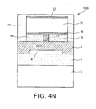
- the gate 12 and the dielectric portions 14 and 16 are covered with a stack of three layers: a first conductive layer 18, a layer 20 based on a piezoelectric material and a second conductive layer 22.
- the conductive layers 18 and 22 serve of electrodes, respectively lower and upper, polarization of the piezoelectric material of the layer 20.
- the material of the conductive layers 18 and 22 may for example be molybdenum and / or platinum, the choice of this material depending on the nature of the material piezoelectric used in the layer 20.
- the stiffness of the material of the conductive layers 18 and 22 is here chosen greater than that of the dielectric material of the dielectric portions 14 and 16.
- the piezoelectric material of the layer 20 may be for example high piezoelectric material such as PMN-PT and / or PZN-PT.
- the layers 18, 20 and 22, as well as the assembly comprising the gate dielectric 10, the gate 12 and the dielectric portions 14 and 16, have, along the x axis represented on the figure 1 , the same length L 2 less than L 1 .
- the piezoelectric layer 20 and the conductive layers 18 and 22 are centered with respect to the axis, or plane, of symmetry of the MOS transistor passing through the middle of the gate 12, between the source and drain zones.
- the gate dielectric 10, the gate 12 and the dielectric portions 14 and 16, portions 23 are deposited on the active layer 6.
- a dielectric material for example SiO 2 .
- the piezoelectric layer 20 extends or is compressed, depending on the sign of the polarization of the gate 12, mainly in the direction of the y axis represented on the figure 1 , according to the configuration of the piezoelectric layer stack 20 / horizontal biasing electrodes 18 and 22.
- the deformations generated along the y axis within the piezoelectric layer 20 are transmitted throughout the structure of the device 100.
- the active layer 6, and therefore the channel of the transistor, is thus constrained biaxially in the plane perpendicular to the y-axis, that is to say a plane parallel to the plane (x, z).
- the piezoelectric effect obtained is all the higher as the surface of the piezoelectric layer facing the polarization electrodes is large.
- the piezoelectric effect generated by the piezoelectric layer must be sufficient.
- the assembly consisting of the piezoelectric layer and its polarization electrodes has a length adapted according to the electromechanical characteristics of the material of the piezoelectric layer.
- the upper electrode 22 has a length along the axis X equal to the length of the piezoelectric layer 20.
- the length of the piezoelectric layer is greater than L G. Given this difference in length, the presence of the lower electrode 18 makes it possible to polarize the piezoelectric layer 20 over its entire length.
- the device 100 may not comprise a lower electrode 18.
- the piezoelectric layer 20 is disposed directly. on the gate 12 which acts as the lower polarization electrode of the piezoelectric layer 20. The piezoelectric layer 20 is thus polarized over its entire length.
- This applied stress makes it possible to increase the current I ON and to reduce the current I OFF of the MOS transistor.
- the influence of the stress on the value of the currents depends on the type of carriers involved, electrons or holes.
- the piezoelectric layer 20 in the on state, that is to say when the gate voltage V G is positive and non-zero, for example equal to about 1 V, the piezoelectric layer 20 is compressed in the y direction and puts the channel of the transistor into biaxial voltage. The carrier mobility and therefore the current I ON are thus increased.
- the off state that is to say when the gate voltage V G is zero, the piezoelectric layer 20 extends in the y direction and biaxially squeezes the channel of the transistor. The carrier mobility and therefore the current I OFF are thus reduced.
- the cavity 8 can be filled with a material whose stiffness is inferior to that of the material of the layer active 6, thus having better properties than the vacuum for the various parasitic phenomena discussed above.
- This material may for example be SiO 2 , and / or a porous material and / or a SOG (Spin-On-Glass) material.
- This possibility of controlling the performance of the device independently of the operation of the MOS transistor is particularly advantageous when the semiconductor device comprises several transistors, allowing for example to increase the leakage currents in a certain branch of a circuit and to reduce them in another.
- FIG. 2 represents a semiconductor device 200 comprising a constrained channel MOS transistor according to a second embodiment.
- the piezoelectric layer 20 and the conductive layers 18 and 22 are off-center with respect to an axis of symmetry 24, or a plane of symmetry, of the MOS transistor.
- an axis of symmetry 26, or a plane of symmetry, of the layers 18, 20 and 22 is off-center by a distance ⁇ with respect to the axis of symmetry 24, or plane of symmetry, of the MOS transistor.
- the distance ⁇ can be taken positive or negative with respect to the axis of symmetry 24 of the MOS transistor, that is to say that the layers 18, 20 and 22 can be decentered as well on one side as on the other.
- This misalignment makes it possible to position the piezoelectric stack formed by the layers 18, 20 and 22 in such a way as to maximize the transmission of the deformations of the piezoelectric layer 20 to the active layer 6. Indeed, the anisotropy of stiffness of certain piezoelectric materials (by PMN-PT) induces a non-uniform deformation field within them.
- the misalignment of the piezoelectric stack makes it possible to place the gate 12 in such a way that the stresses are as high and homogeneous as possible in the transistor channel.
- This misalignment also implies that the dielectric portions 14 and 16 are not of the same length (dimension along the x axis represented on FIG. figure 2 ), the dielectric portion 14 having a length greater than that of the dielectric portion 16 in the example of the figure 2 .
- FIG. 3 represents a semiconductor device 300 comprising a variable-constrained channel MOS transistor according to a third embodiment.
- the set of layers 18, 20 and 22 is here in contact with the upper face of the gate 12 but only overcomes the source region of the transistor in this example on the left side of the gate stack.
- This asymmetrical arrangement of the piezoelectric stack of the layers 18, 20 and 22 with respect to the gate 12 of the transistor can be used to deform the shear transistor channel. The constraint within the channel will then be very inhomogeneous.
- only a dielectric portion, here the dielectric portion 14, is disposed next to the gate stack.
- the effects of the misalignment can be quantified by incrementing the distance ⁇ , representing the distance separating the axis of symmetry 24 of the transistor and the axis of symmetry 26 of the piezoelectric stack, ⁇ being, in this third embodiment, equal to about half a length of the piezoelectric layer 20, from a simulation to the next.
- ⁇ 0
- the surface of the structure of the MOS transistor formed by the upper faces of the gate 12 and the insulating portion or portions 14, 16, being flat it is possible, in addition to the use of piezoelectric materials obtained by deposition to form the piezoelectric layer 20, to use monocrystalline piezoelectric materials in thin layers transferred by bonding. This expands the choice of piezoelectric materials for the realization of the structure.
- certain monocrystalline piezoelectric materials exhibit very high piezoelectric coefficients, for example PMN-PT and PZN-PT (d 33 (PMN-PT) ⁇ 2404 ⁇ m / V, in comparison with the thin films obtained by deposition: d 33 (thin ceramic films of PZT) ⁇ 80).
- a method for producing the semiconductor device 100 according to a first embodiment will now be described in connection with the Figures 4A to 40 .
- an SOI substrate is formed from the substrate 2, the dielectric layer 4, and a semiconductor active layer 6 here based on silicon, for example with a thickness of about 5 nm.
- a layer 104 and then a layer 106 are deposited successively on active layer 6.
- the material of layer 106 is similar to that of active layer 6 ( Figure 4B ).
- the material of the layer 104 is chosen such that it can be etched selectively with respect to the material of the layers 6 and 106, for example SiGe.
- the thickness of the layer 104 is for example equal to about 20 nm, that of the layer 106 being for example equal to about 15 nm.
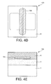
- a vertical anisotropic etching of the layers 104 and 106 is then carried out so as to form portions of the layers 104 and 106 whose shape is substantially similar to that of the cavity 8 intended to be formed in the device 100, but of dimensions a little lower than those of the future cavity 8 ( Figures 4C and 4D , the figure 4D being a view from above).
- a silicon epitaxy of the layer 6 is made, so that the remaining portion of the layer of SiGe 104 is completely surrounded by the silicon of the active layer 6.
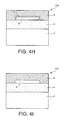
- Oxidation of the silicon of the walls 110 of the cavity 8 is then carried out ( Figure 4H ). This oxidation is at least achieved such that the silicon portion of the active layer 6 between the cavity 8 and the oxide layer 4 is completely oxidized.
- the silicon oxide 110 formed in the cavity 8 is removed by selective etching with respect to the silicon of the active layer 6.
- the cavity 8 is thus formed.
- a wall of the cavity 8 is formed by a part of the dielectric layer 4.
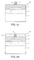
- a MOS transistor having an active zone comprising a source zone, a drain zone and a channel made in the active layer 6 is then produced.
- the channel of this MOS transistor is produced above the cavity 8.
- a dielectric of gate 10 and a gate 12 are formed on the channel of the transistor.
- a dielectric layer is then deposited on the active layer 6 and on the gate 12.
- a planarization of this dielectric layer is then implementation, with stop at the gate 12, such that the surface of this dielectric layer is at the upper face of the gate 12.
- the dielectric layer forms, on either side of the stack gate, dielectric portions 14 and 16 ( figure 4K ).
- the dielectric-based layer may be replaced by a resin-based layer, thus forming resin portions on either side of the gate 12, replacing the dielectric portions 14 and 16.
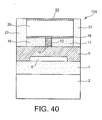
- a dielectric deposit 23 is made around the locations previously etched and on the layer 22, then planarization of the upper surface of the structure formed with stop at the level of the conductive layer 22.
- the steps represented on the Figures 4A to 4K in order to form a structure comprising the substrate 2, the dielectric layer 4, the active layer 6, the cavity 8, the gate dielectric 10, the gate 12 and the dielectric portions 14 and 16.
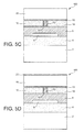
- a substrate 120 based on a monocrystalline piezoelectric material is coated with the electrically conductive layer 18.
- An ion implantation is then carried out in the substrate 120 through the conductive layer 18, followed by annealing for the diffusion of the implanted ions, forming a delimitation 119 separating the substrate 120 into two parts 122 and 20 ( Figure 5B ).
- the portion 20 of the substrate 120 in contact with the conductive layer 18 forms the thin layer which will be transferred to the transistor.
- Parts 122 and 20 are then separated from one another.
- the thin layer 20, for example of a thickness equal to about 100 nm, thus obtained, is obtained by a Smart-Cut TM method covered with the conductive layer. 18, for example of thickness equal to about 10 nm.
- the piezoelectric thin film 20 is then adhesively bonded to the grid 12 and the dielectric portions 14 and 16 via the conductive layer 18 by molecular adhesion.
- the conductive layer 22 is then deposited on the piezoelectric layer 20, forming the upper electrode of the gate stack of the device 100 ( figure 5D ).
- the device 100 is then completed as for the first embodiment by the steps represented on the Figures 4M to 40 .
- the surface of the lower electrode layer 18 is planar so that the molecular bonding mechanism can be used for a piezoelectric layer based on a monocrystalline material.
Abstract
Description
L'invention concerne le domaine des circuits intégrés, et plus particulièrement celui des transistors tels que les transistors MOS.The invention relates to the field of integrated circuits, and more particularly that of transistors such as MOS transistors.
Un moyen d'augmenter le courant ION, c'est-à-dire le courant de saturation à l'état passant, des dispositifs microélectroniques de type MOS consiste à mettre à profit les contraintes mécaniques induites par les procédés technologiques mis en oeuvre au cours de la fabrication des transistors pour améliorer la mobilité des porteurs de charges (trous pour les transistors PMOS et électrons pour les transistors NMOS).One way of increasing the current I ON , that is to say the saturation current in the on state, of the microelectronic devices of the MOS type is to take advantage of the mechanical stresses induced by the technological processes implemented in during the fabrication of transistors to improve the mobility of charge carriers (holes for PMOS transistors and electrons for NMOS transistors).
Différentes méthodes ont déjà été mises au point dans le but de mettre en contrainte le canal d'un transistor.Different methods have already been developed in order to constrain the channel of a transistor.
Dans les dispositifs réalisés en technologie CMOS, des couches à base de nitrure, déposées de manière conforme à la surface de la structure d'un transistor MOS, permettent d'appliquer une contrainte uniaxiale en tension dans le canal d'un transistor NMOS et une contrainte uniaxiale en compression dans celui d'un transistor PMOS. Ces contraintes permettent d'augmenter la mobilité des porteurs et donc d'augmenter proportionnellement le courant ION du transistor. Mais à l'état bloqué, ces contraintes réduisent la masse effective des porteurs, augmentant ainsi les courants de fuites par effet tunnel, notamment lorsque la longueur de grille est faible, et réduisant donc les performances du transistor à l'état « OFF » en augmentant la consommation du transistor dans cet état « OFF ».In devices made in CMOS technology, nitride-based layers, deposited conformably to the surface of the structure of a MOS transistor, make it possible to apply a uniaxial stress in the channel of an NMOS transistor and a uniaxial stress in compression in that of a PMOS transistor. These constraints make it possible to increase the mobility of the carriers and therefore to proportionally increase the current I ON of the transistor. But in the blocked state, these constraints reduce the effective mass of the carriers, thus increasing the tunneling leakage currents, especially when the gate length is low, and thus reducing the transistor's performance in the "OFF" state by increasing the consumption of the transistor in this "OFF" state.
Le document
Dans un tel transistor, les performances en terme de vitesse et de consommation, reposant sur un changement de résistivité du matériau du canal, et en particulier le rapport entre le courant de saturation et le courant de fuite, sont insuffisantes pour les applications de masse des transistors. De plus, la réalisation d'un tel transistor au niveau industriel s'avère onéreuse dans la mesure où le MoC est un matériau coûteux. Enfin, un tel dispositif n'est pas réalisable en technologie CMOS.In such a transistor, the performances in terms of speed and consumption, based on a resistivity change of the channel material, and in particular the ratio between the saturation current and the leakage current, are insufficient for the mass applications of transistors. In addition, the production of such a transistor at the industrial level is expensive since MoC is an expensive material. Finally, such a device is not feasible in CMOS technology.
Le document
Toutefois, compte tenu de la géométrie du dispositif, seuls des matériaux piézoélectriques pouvant être obtenus par dépôt peuvent être utilisés (par exemple des céramiques PZT, dont les coefficients piézoélectriques sont faibles : d33 ≈ 80 pm/V et d31 ≈ -40 pm/V, d33 étant un coefficient décrivant la déformation du matériau piézoélectrique selon une direction parallèle au vecteur de polarisation de la couche piézoélectrique, c'est-à-dire la déformation en épaisseur, d31 étant un coefficient décrivant la déformation du matériau piézoélectrique selon une direction orthogonale au vecteur de polarisation de la couche piézoélectrique, c'est-à-dire la déformation en largeur). Avec de tels matériaux piézoélectriques, la contrainte maximale pouvant être obtenue à la surface du canal est par exemple inférieure à 100 MPa pour un transistor ayant une longueur de grille égale à 40 nm et une épaisseur de la couche piézoélectrique égale à 300 nm, ce qui limite considérablement les gains en terme d'augmentation du courant ION et de réduction du courant IOFF.However, given the geometry of the device, only piezoelectric materials obtainable by deposition can be used (for example PZT ceramics, whose piezoelectric coefficients are low: d 33 ≈ 80 pm / V and d 31 ≈ -40 pm / V, d 33 being a coefficient describing the deformation of the piezoelectric material in a direction parallel to the polarization vector of the piezoelectric layer, that is to say the deformation in thickness, d 31 being a coefficient describing the deformation of the piezoelectric material in a direction orthogonal to the polarization vector of the piezoelectric layer, that is to say the deformation in width). With such piezoelectric materials, the maximum stress that can be obtained on the surface of the channel is, for example, less than 100 MPa for a transistor having a gate length equal to 40 nm and a piezoelectric layer thickness equal to 300 nm, which considerably limits the gains in terms of increase of current I ON and reduction of current I OFF .
De plus, dans ce type de structure, la couche piézoélectrique est polarisée par ses surfaces en contact avec, d'une part le matériau conducteur de grille, et d'autre part avec la région de source et/ou de drain du transistor. Ainsi, le champ électrique appliqué à la couche piézoélectrique est maximal dans la région située à proximité de l'oxyde de grille et est donc inhomogène dans la couche piézoélectrique. Pour ne pas détériorer le dispositif, la valeur maximale du champ électrique appliqué dans cette région doit rester inférieure à la valeur du champ de claquage du matériau piézoélectrique (par exemple, pour une couche mince à base de céramique PZT, Eclaquage ≈ 800 kV/cm). Pour une différence de potentiel de 1 V, le champ électrique dans la couche piézoélectrique reste inférieur à son champ de claquage pour des épaisseurs d'oxyde supérieures à 12,5 nm dans le cas d'une céramique de PZT (distance inter-électrodes mini = 1 V/800 kV·cm-1 = 12, 5 nm). Cette structure n'est donc pas adaptée pour induire une contrainte dans le canal de transistors MOS d'épaisseurs d'oxyde de grille inférieures à 10 nm.Moreover, in this type of structure, the piezoelectric layer is polarized by its surfaces in contact with, on the one hand, the gate-conducting material, and on the other hand with the source and / or drain region of the transistor. Thus, the electric field applied to the piezoelectric layer is maximum in the region located near the gate oxide and is therefore inhomogeneous in the piezoelectric layer. In order not to damage the device, the maximum value of the electric field applied in this region must remain lower than the value of the breakdown field of the piezoelectric material (for example, for a ceramic-based thin layer PZT, E breakdown ≈ 800 kV / cm). For a potential difference of 1 V, the electric field in the piezoelectric layer remains below its breakdown field for oxide thicknesses greater than 12.5 nm in the case of a PZT ceramic (minimum inter-electrode distance = 1 V / 800 kV · cm -1 = 12.5 nm). This structure is therefore not suitable for inducing a constraint in the MOS transistor channel of gate oxide thicknesses less than 10 nm.
Un but de la présente invention est de proposer une nouvelle structure de transistor MOS aux performances électriques améliorées : augmentation du courant ION et réduction du courant IOFF par rapport aux dispositifs de l'art antérieur, permettant une plus grande vitesse de fonctionnement des dispositifs et une consommation moindre à l'état OFF, et pouvant comporter un oxyde de grille dont l'épaisseur puisse être inférieure aux limites imposées par les dispositifs de l'art antérieur, par exemple inférieure à environ 10 nm.An object of the present invention is to provide a novel structure of MOS transistor with improved electrical performance: increase of the current I ON and reduction of the current I OFF compared to the devices of the prior art, allowing a greater speed of operation of the devices and less consumption in the OFF state, and may include a gate oxide whose thickness may be less than the limits imposed by the devices of the prior art, for example less than about 10 nm.
Ce dispositif repose sur l'application d'une contrainte mécanique d'intensité variable dans le canal d'un transistor MOS, indépendamment de sa longueur de grille.This device is based on the application of a mechanical stress of variable intensity in the channel of a MOS transistor, regardless of its gate length.
La présente invention concerne une nouvelle structure de transistor MOS dont il est possible de faire varier l'état de contrainte au sein du canal en fonction de la tension de grille. Elle repose sur l'utilisation d'une couche piézoélectrique permettant d'induire une contrainte d'amplitude variable et de direction variable dans la région du canal d'un transistor MOS.The present invention relates to a new MOS transistor structure whose strain state within the channel can be varied as a function of the gate voltage. It is based on the use of a piezoelectric layer for inducing a variable amplitude and variable direction of stress in the region of the channel of a MOS transistor.
Pour cela, la présente invention propose un dispositif semi-conducteur comportant au moins :
- un substrat,
- un transistor comprenant au moins une région de source, une région de drain, un canal et une grille,
- une couche à base d'au moins un matériau piézoélectrique, reposant au moins sur la grille et apte à induire au moins une contrainte mécanique sur le canal du transistor selon une direction sensiblement perpendiculaire au plan d'une face de la couche piézoélectrique se trouvant du côté de la grille,
- a substrate,
- a transistor comprising at least one source region, one drain region, one channel and one gate,
- a layer based on at least one piezoelectric material, resting at least on the gate and capable of inducing at least one mechanical stress on the transistor channel in a direction substantially perpendicular to the plane of a face of the piezoelectric layer lying in the side of the grid,
Contrairement à certains dispositifs de l'art antérieur dans lesquels la grille réduit la transmission des déformations générées au sein de la couche piézoélectrique, la couche piézoélectrique, qui peut être plane, est placée sur la face supérieure de la grille du transistor, sans être directement disposée sur les zones de source et de drain. On tire ainsi profit de la présence de la grille pour transmettre les déformations générées au sein de la couche piézoélectrique jusqu'au canal, permettant d'obtenir des contraintes supérieures à 100 MPa dans le canal.Unlike some devices of the prior art in which the gate reduces the transmission of deformations generated within the piezoelectric layer, the piezoelectric layer, which can be flat, is placed on the upper face of the gate of the transistor, without being directly disposed on the source and drain areas. This benefits from the presence of the gate to transmit the deformations generated within the piezoelectric layer to the channel, making it possible to obtain stresses greater than 100 MPa in the channel.
La couche piézoélectrique est polarisée grâce aux deux électrodes entre lesquelles se trouve ladite couche piézoélectrique, une électrode étant formée sur la couche piézoélectrique, indépendamment des dimensions de la structure MOS elle-même. L'invention peut donc s'appliquer pour des longueurs de grille et des épaisseurs d'oxyde de grille très faibles, pouvant être respectivement égales à environ 10 nm et de 0,5 nm.The piezoelectric layer is polarized by virtue of the two electrodes between which said piezoelectric layer is located, an electrode being formed on the piezoelectric layer, independently of the dimensions of the MOS structure itself. The invention can therefore be applied for very small gate lengths and gate oxide thicknesses, which can be equal to approximately 10 nm and 0.5 nm, respectively.
La planarisation de la surface de la structure du transistor MOS formée notamment par la face supérieure de la grille, et le fait la couche piézoélectrique ne soit pas déposée sur les zones de source et de drain, permet, en plus de l'utilisation de matériaux piézoélectriques obtenus par dépôt tels que les céramiques PZT pour former la couche piézoélectrique, d'utiliser des matériaux piézoélectriques monocristallins en couches minces reportées par collage. Ceci élargit le choix des matériaux piézoélectriques pour la réalisation de la structure. De plus, certains matériaux piézoélectriques monocristallins présentent des coefficients piézoélectriques très élevés, à l'exemple du PMN-PT et/ou du PZN-PT (d33(PMN-PT) ≈ 2404 pm/V). L'utilisation de matériaux piézoélectriques à coefficients piézoélectriques très élevés présente l'avantage d'accroître les niveaux de contrainte obtenus au niveau du canal, et ainsi d'augmenter les performances du transistor.The planarization of the surface of the structure of the MOS transistor formed in particular by the upper face of the gate, and the fact that the piezoelectric layer is not deposited on the source and drain zones, allows, in addition to the use of materials deposited piezoelectric such as PZT ceramics to form the piezoelectric layer, to use monocrystalline piezoelectric materials in thin layers reported by gluing. This expands the choice of piezoelectric materials for the realization of the structure. In addition, some monocrystalline piezoelectric materials have very high piezoelectric coefficients, for example PMN-PT and / or PZN-PT (d 33 (PMN-PT) ≈ 2404 μm / V). Use piezoelectric materials with very high piezoelectric coefficients has the advantage of increasing the stress levels obtained at the channel, and thus to increase the performance of the transistor.
L'utilisation d'une couche piézoélectrique comme générateur de déformations permet d'induire au sein du canal un état de contrainte de direction et d'amplitude variables, contrôlées respectivement par le signe et la valeur de la polarisation appliquée aux bornes de la couche piézoélectrique, qui avantageusement peut être la même que celle appliquée sur la grille. La tension destinée à être appliquée à la grille du transistor peut être similaire à la tension destinée à être appliquée à la couche piézoélectrique.The use of a piezoelectric layer as a deformation generator makes it possible to induce in the channel a state of constraint of variable direction and amplitude, controlled respectively by the sign and the value of the polarization applied across the piezoelectric layer. which advantageously may be the same as that applied to the grid. The voltage to be applied to the gate of the transistor may be similar to the voltage to be applied to the piezoelectric layer.
La couche piézoélectrique et/ou la première couche conductrice peuvent être planes.The piezoelectric layer and / or the first conductive layer may be planar.
Les dimensions des faces des électrodes en contact avec la couche piézoélectrique peuvent être supérieures ou égales aux dimensions des faces de la couche piézoélectrique en contact avec les électrodes. Ainsi, le champ électrique créé par la tension appliquée sur les électrodes de polarisation, entre lesquelles se trouve la couche piézoélectrique, est uniforme dans toute la couche piézoélectrique. Ce champ électrique uniforme implique une contrainte uniforme appliquée ensuite dans tout le canal par la couche piézoélectrique.The dimensions of the faces of the electrodes in contact with the piezoelectric layer may be greater than or equal to the dimensions of the faces of the piezoelectric layer in contact with the electrodes. Thus, the electric field created by the voltage applied to the bias electrodes, between which is the piezoelectric layer, is uniform throughout the piezoelectric layer. This uniform electric field implies a uniform stress then applied throughout the channel by the piezoelectric layer.
Dans une première variante, l'autre des deux électrodes de polarisation peut être formée par la grille du transistor.In a first variant, the other of the two polarization electrodes may be formed by the gate of the transistor.
Dans une seconde variante, l'autre des deux électrodes de polarisation peut être formée par une seconde couche à base d'au moins un matériau électriquement conducteur disposée entre la couche piézoélectrique et la grille du transistor.In a second variant, the other of the two polarization electrodes may be formed by a second layer based on at least one electrically conductive material disposed between the piezoelectric layer and the gate of the transistor.
Dans ce cas, le dispositif peut comporter en outre une couche diélectrique disposée entre la grille et la seconde couche à base de matériau conducteur. Cette couche diélectrique permet d'isoler l'électrode de polarisation, formée par la seconde couche conductrice, de la grille du transistor, permettant ainsi une commande indépendante du transistor (par l'intermédiaire de la grille) et de la couche piézoélectrique (par l'intermédiaire des électrodes de polarisation).In this case, the device may further comprise a dielectric layer disposed between the grid and the second layer based on conductive material. This dielectric layer makes it possible to isolate the polarization electrode, formed by the second conductive layer, from the gate of the transistor, thus allowing independent control of the transistor (via the gate) and the piezoelectric layer (by way of FIG. intermediate polarization electrodes).
La première couche conductrice et/ou, lorsque le dispositif comporte une seconde couche conductrice, la seconde couche conductrice peuvent être sensiblement planes et parallèles à la couche piézoélectrique.The first conductive layer and / or, when the device comprises a second conductive layer, the second conductive layer may be substantially flat and parallel to the piezoelectric layer.
Dans le dispositif selon l'invention, la rigidité de l'empilement de grille peut être mise à profit : elle peut participer à la transmission de la déformation générée par la couche piézoélectrique jusqu'à la surface du canal. En effet, lorsque la longueur de grille Lg du transistor est réduite, l'homme de métier tend à remplacer une grille peu rigide, par exemple à base de polysilicium, par une grille métallique plus rigide, par exemple à base de TiN (E(TiN) ≈ 290 GPa, et E(Si) ≈ 130 GPa, avec E coefficient de raideur du matériau ou module d'Young). Cette rigidité peut être très néfaste dans le cas où la couche piézoélectrique est déposée de manière conforme sur la surface du transistor (sur la grille et sur les zones de source et de drain), comme décrit dans le document
La rigidité des couches conductrices formant des électrodes peut également être mise à profit : d'après la direction des déformations selon un axe sensiblement perpendiculaire au plan de la face de la couche piézoélectrique se trouvant du côté de la grille, elles participent, de manière analogue à la grille, à la transmission des déformations générées dans la couche piézoélectrique à la grille. La ou les couches conductrices peuvent être à base de molybdène et/ou de platine. Dans le cas d'une couche piézoélectrique déposée de façon conforme à la surface du transistor et polarisée par des électrodes horizontales, ces électrodes, à base d'un matériau, par exemple du molybdène ou du platine, très rigide par rapport au silicium du canal (E(Mo) ≈ 320 GPa, E(Pt) ≈ 276 GPa alors que E(Si) ≈ 130 MPa) fixent toute la surface du transistor. L'électrode inférieure agit ainsi comme une barrière à la transmission de déformations générées selon une direction dans le plan de la face de la couche piézoélectrique se trouvant du côté de la grille. Elle concentre en son sein les déformations, celles-ci n'étant que très faiblement transmises à la surface du canal. Il est ainsi difficile d'induire des contraintes au sein du canal.The rigidity of the conductive layers forming electrodes can also be exploited: according to the direction of the deformations along an axis substantially perpendicular to the plane of the face of the piezoelectric layer on the side of the gate, they participate, in a similar way to the grid, to the transmission of the deformations generated in the piezoelectric layer to the grid. The conductive layer or layers may be based on molybdenum and / or platinum. In the case of a piezoelectric layer deposited conformably to the surface of the transistor and polarized by horizontal electrodes, these electrodes, based on a material, for example molybdenum or platinum, which is very rigid with respect to the silicon of the channel (E (Mo) ≈ 320 GPa, E (Pt) ≈ 276 GPa while E (Si) ≈ 130 MPa) fix the entire surface of the transistor. The lower electrode thus acts as a barrier to the transmission of deformations generated along a direction in the plane of the face of the piezoelectric layer on the grid side. It concentrates within it the deformations, these being only very slightly transmitted to the surface of the channel. It is thus difficult to induce constraints within the channel.
Grâce à la structure selon l'invention, la contrainte induite peut être localisée sous la grille, et plus précisément à proximité d'une interface diélectrique de grille/substrat qui correspond à la zone d'inversion du canal selon le mode de fonctionnement d'un transistor MOS. Il s'agit de la zone de transport des porteurs et donc celle où la contrainte peut être le plus fortement appliquée afin de profiter au maximum de ses effets sur les performances électriques du transistor.Thanks to the structure according to the invention, the induced stress can be located under the gate, and more precisely in the vicinity of a gate / substrate dielectric interface which corresponds to the inversion zone of the channel according to the mode of operation of a MOS transistor. This is the carrier transport zone and therefore the one where the stress can be most strongly applied in order to take maximum advantage of its effects on the electrical performance of the transistor.
Lorsque l'électrode inférieure de polarisation du matériau piézoélectrique, c'est-à-dire la couche conductrice se trouvant entre la couche piézoélectrique et le substrat, est en contact avec la grille sur toute la largeur de celle-ci (la largeur correspondant à la direction transverse au canal), la résistivité de la grille peut être réduite, ce qui implique que le temps de polarisation de la grille sur toute sa largeur, et donc le temps de fonctionnement du transistor, peut être réduit.When the lower polarization electrode of the piezoelectric material, that is to say the conductive layer between the piezoelectric layer and the substrate, is in contact with the grid over the entire width thereof (the width corresponding to the direction transverse to the channel), the resistivity of the gate can be reduced, which implies that the polarization time of the gate over its entire width, and therefore the operating time of the transistor, can be reduced.
La structure du dispositif favorise également son fonctionnement mécanique et correspond à un procédé technologique standard de fabrication d'un transistor MOS.The structure of the device also promotes its mechanical operation and corresponds to a standard technological process for manufacturing a MOS transistor.
Le dispositif semi-conducteur peut comporter en outre au moins une portion à base d'au moins un matériau diélectrique disposée sur le substrat et à côté de la grille, recouvrant au moins une partie de la zone de source ou de drain, la couche piézoélectrique reposant également sur cette portion diélectrique.The semiconductor device may further comprise at least one portion based on at least one dielectric material disposed on the substrate and next to the gate, covering at least a portion of the source or drain zone, the piezoelectric layer. also resting on this dielectric portion.
Le dispositif semi-conducteur peut comporter en outre une seconde portion d'au moins un matériau diélectrique disposée sur le substrat et à côté de la grille, sur laquelle peut reposer la couche piézoélectrique, les zones de source et de drain pouvant être au moins recouvertes en partie par les portions diélectriques.The semiconductor device may further comprise a second portion of at least one dielectric material disposed on the substrate and next to the gate, on which the piezoelectric layer may rest, the source and drain zones. at least partially covered by the dielectric portions.
Le dispositif selon l'invention tire avantageusement profit de la ou des portions diélectriques, par exemple à base de SiO2, de part et d'autre de la grille car le SiO2 est un matériau mécaniquement peu rigide. Ainsi, le mode de déformation longitudinale de la couche piézoélectrique est favorisé car ses bords verticaux sont libres de se déformer le plus possible.The device according to the invention advantageously takes advantage of the dielectric portion or portions, for example based on SiO 2 , on either side of the gate because the SiO 2 is a mechanically inflexible material. Thus, the mode of longitudinal deformation of the piezoelectric layer is favored because its vertical edges are free to deform as much as possible.
Par ailleurs, avantageusement, la surface supérieure de la couche piézoélectrique peut être fixée le plus rigidement possible afin que les déformations soient transmises de préférence vers le bas, du côté du transistor et non pas aux matériaux situés au-dessus de la couche piézoélectrique. Cette condition peut être obtenue intrinsèquement lorsque les niveaux d'interconnexions sont nombreux (ce qui est le cas dans les circuits complexes comportant jusqu'à 10 niveaux de métal) et peut être favorisée expérimentalement par le dépôt d'une couche servant d'électrode supérieure constituée d'un matériau très rigide, par exemple du platine ou du molybdène.Furthermore, advantageously, the upper surface of the piezoelectric layer can be fixed as rigidly as possible so that the deformations are preferably transmitted downwards, on the transistor side and not to the materials situated above the piezoelectric layer. This condition can be intrinsically obtained when the interconnection levels are numerous (which is the case in complex circuits with up to 10 metal levels) and can be experimentally favored by the deposition of a layer serving as upper electrode. made of a very rigid material, for example platinum or molybdenum.
Enfin, ce dispositif tire avantageusement profit du mode de déformation longitudinale du matériau piézoélectrique ce qui constitue un avantage en terme de procédé par rapport à la réalisation d'électrodes verticales qui peuvent être utilisées avantageusement pour profiter du mode de déformation transversal du matériau piézoélectrique. En effet, le dimensionnement des électrodes est mieux maîtrisé dans le cas d'électrodes horizontales, c'est-à-dire dans le plan de la face de la couche piézoélectrique se trouvant du côté de la grille, formées par une couche mince conductrice qui peut être obtenue par dépôt, croissance, report..., que dans le cas d'électrodes verticales posant des problèmes lors de la gravure verticale du matériau constituant les électrodes.Finally, this device advantageously takes advantage of the longitudinal deformation mode of the piezoelectric material which is an advantage in terms of process compared to the production of vertical electrodes which can be advantageously used to take advantage of the transverse deformation mode of the piezoelectric material. Indeed, the sizing of the electrodes is better controlled in the case horizontal electrodes, that is to say in the plane of the face of the piezoelectric layer located on the side of the gate, formed by a conductive thin layer which can be obtained by deposition, growth, transfer ..., in the case of vertical electrodes posing problems in the vertical etching of the material constituting the electrodes.
Le dispositif semi-conducteur peut comporter en outre une couche diélectrique disposée entre la grille et la couche piézoélectrique.The semiconductor device may further comprise a dielectric layer disposed between the gate and the piezoelectric layer.
Le transistor peut être avantageusement de type MOS.The transistor may advantageously be of the MOS type.
Le substrat peut comporter une couche à base d'un matériau semi-conducteur, sur laquelle sont empilées une couche diélectrique et une couche active à base d'un matériau semi-conducteur.The substrate may comprise a layer based on a semiconductor material, on which are stacked a dielectric layer and an active layer based on a semiconductor material.
Le substrat peut comporter une cavité formée au moins sous le canal du transistor.The substrate may comprise a cavity formed at least under the channel of the transistor.
La cavité peut être remplie d'au moins un matériau dont la raideur peut être inférieure à celle du matériau du substrat.The cavity may be filled with at least one material whose stiffness may be less than that of the substrate material.
La grille peut être à base de polysilicium et/ou de nitrure de titane et/ou de nitrure de tantale.The grid may be based on polysilicon and / or titanium nitride and / or tantalum nitride.
La raideur du matériau de la grille peut être supérieure à la raideur du matériau de la ou des portions diélectriques.The stiffness of the material of the grid may be greater than the stiffness of the material of the dielectric portion or portions.
Le rapport de la raideur du matériau de la grille sur la raideur du matériau de la ou des portions diélectriques peut être supérieur à 1, et par exemple compris entre environ 2 et 5.The ratio of the stiffness of the material of the grid to the stiffness of the material of the dielectric portion or portions may be greater than 1, for example between about 2 and 5.
Lorsque la couche piézoélectrique est disposée entre deux couches conductrices, la raideur du matériau des couches conductrices peut être supérieure à la raideur du matériau des portions diélectriques.When the piezoelectric layer is disposed between two conductive layers, the stiffness of the material of the conductive layers may be greater than the stiffness of the material of the dielectric portions.
La couche piézoélectrique peut être symétrique par rapport à un premier plan sensiblement perpendiculaire au plan de la face de la couche piézoélectrique se trouvant du côté de la grille, la grille pouvant être symétrique par rapport à un second plan sensiblement perpendiculaire audit plan de la face de la couche piézoélectrique se trouvant du côté de la grille, les premier et second plans pouvant être superposés ou décalés l'un par rapport à l'autre.The piezoelectric layer may be symmetrical with respect to a first plane substantially perpendicular to the plane of the face of the piezoelectric layer on the side of the gate, the gate being symmetrical with respect to a second plane substantially perpendicular to said plane of the face of the the piezoelectric layer being on the side of the gate, the first and second planes being superposable or offset with respect to each other.
La présente invention concerne également un procédé de réalisation d'un dispositif semi-conducteur comportant au moins les étapes de :
- réalisation d'un transistor comprenant au moins une région de source, une région de drain, un canal et une grille sur un substrat,
- dépôt d'une couche à base d'au moins un matériau piézoélectrique au moins au-dessus de la grille, la couche piézoélectrique étant apte à induire au moins une contrainte mécanique sur le canal du transistor selon une direction perpendiculaire au plan d'une face de la couche piézoélectrique se trouvant du côté de la grille,
- dépôt d'une couche à base d'au moins un matériau électriquement conducteur formant une première électrode de polarisation tel que la couche piézoélectrique soit disposée entre cette couche conductrice et la grille du transistor,
- producing a transistor comprising at least one source region, a drain region, a channel and a gate on a substrate,
- deposition of a layer based on at least one piezoelectric material at least above the gate, the piezoelectric layer being able to induce at least one mechanical stress on the transistor channel in a direction perpendicular to the plane of a face the piezoelectric layer on the grid side,
- deposition of a layer based on at least one electrically conductive material forming a first polarization electrode such that the piezoelectric layer is disposed between this conductive layer and the gate of the transistor,
Le procédé peut comporter en outre, entre l'étape de réalisation du transistor et l'étape de dépôt de la couche piézoélectrique, une étape de dépôt d'une autre couche à base d'au moins un matériau électriquement conducteur au moins au-dessus de la grille, la couche piézoélectrique pouvant être ensuite déposée sur cette autre couche conductrice formant la seconde électrode de polarisation.The method may furthermore comprise, between the step of producing the transistor and the step of depositing the piezoelectric layer, a step of deposition of another layer based on at least one electrically conductive material at least above of the gate, the piezoelectric layer may then be deposited on this other conductive layer forming the second polarization electrode.
Le procédé peut également comporter, avant l'étape de dépôt de l'autre couche à base de matériau électriquement conducteur, une étape de dépôt d'une couche diélectrique sur la grille, ladite autre couche à base de matériau électriquement conducteur étant déposée sur la couche diélectrique.The method may also comprise, before the deposition step of the other layer based on electrically conductive material, a step of depositing a dielectric layer on the grid, said other layer based on electrically conductive material being deposited on the dielectric layer.
Dans une autre variante, le procédé peut comporter en outre, entre l'étape de réalisation du transistor et l'étape de dépôt de la couche piézoélectrique, une étape de réalisation de la couche piézoélectrique et d'une autre couche à base d'au moins un matériau électriquement conducteur par implantation ionique dans un substrat à base du matériau piézoélectrique comportant ladite autre couche conductrice sur une de ses faces, et par fracture au niveau de l'implantation réalisée dans le substrat, ladite autre couche conductrice pouvant être disposée contre la grille lors de l'étape de dépôt de la couche piézoélectrique.In another variant, the method may furthermore comprise, between the step of producing the transistor and the step of depositing the piezoelectric layer, a step of producing the piezoelectric layer and another layer based on least an electrically conductive material by ion implantation in a substrate based on the piezoelectric material comprising said other conductive layer on one of its faces, and by fracture at the implantation made in the substrate, said other conductive layer being able to be arranged against the gate during the deposition step of the piezoelectric layer.
Le procédé peut comporter en outre, avant l'étape de réalisation du transistor, une étape de réalisation d'une cavité dans le substrat, destinée à être disposée sous le canal du transistor.The method may further comprise, before the step of producing the transistor, a step of forming a cavity in the substrate intended to be arranged under the channel of the transistor.
La réalisation de la cavité peut être obtenue par la mise en oeuvre des étapes suivantes :
- dépôt d'une première couche sur le substrat et d'une seconde couche, à base d'un matériau similaire à celui du substrat, sur la première couche, la première couche étant à base d'un matériau pouvant être gravé sélectivement par rapport aux matériaux du substrat et de la seconde couche,
- gravure anisotrope des premières et secondes couches telles que le motif formé par la portion restante de la première couche soit sensiblement similaire au motif de la cavité, avec arrêt au niveau du substrat,
- épitaxie du matériau du substrat tel que le substrat et la seconde couche forme une couche active du substrat encapsulant la portion restante de la première couche,
- réalisation d'une ouverture dans la couche active pour accéder à la portion restante de la première couche,
- gravure sélective du matériau de la portion restante de la première couche, formant la cavité.
- depositing a first layer on the substrate and a second layer, based on a material similar to that of the substrate, on the first layer, the first layer being based on a material that can be etched selectively with respect to Substrate and second layer materials,
- anisotropic etching of the first and second layers such that the pattern formed by the remaining portion of the first layer is substantially similar to the pattern of the cavity, with a stop at the substrate,
- epitaxial growth of the substrate material such as the substrate and the second layer forms an active layer of the substrate encapsulating the remaining portion of the first layer,
- making an opening in the active layer to access the remaining portion of the first layer,
- selective etching of the material of the remaining portion of the first layer, forming the cavity.
Le procédé peut comporter en outre, lorsque le substrat est du type semi-conducteur sur isolant, après l'étape de gravure sélective du matériau de la portion restante de la première couche, les étapes supplémentaires de :
- oxydation des parois de la cavité,
- gravure sélective de l'oxyde formée au niveau des parois tel qu'une partie de l'isolant du substrat forme une paroi de la cavité.
- oxidation of the walls of the cavity,
- selective etching of the oxide formed at the walls such that a portion of the insulator of the substrate forms a wall of the cavity.
Le procédé peut comporter en outre, après la réalisation de la cavité, une étape de remplissage de la cavité par au moins un matériau dont la raideur est inférieure à celle du matériau du substrat.The method may further comprise, after the production of the cavity, a step of filling the cavity with at least one material whose stiffness is less than that of the material of the substrate.
Le procédé peut comporter en outre, entre l'étape de réalisation du transistor et l'étape de dépôt de la couche piézoélectrique, une étape de dépôt d'au moins une portion à base d'au moins un matériau diélectrique sur le substrat, pouvant recouvrir au moins une partie de la zone de source ou de drain, à côté de la grille, la couche piézoélectrique pouvant être ensuite déposée au-dessus de la portion diélectrique.The method may furthermore comprise, between the step of producing the transistor and the step of depositing the piezoelectric layer, a step of deposition of at least one portion based on at least one dielectric material on the substrate, which can covering at least a portion of the source or drain zone, next to the gate, the piezoelectric layer can then be deposited above the dielectric portion.
Le procédé peut comporter en outre, entre l'étape de réalisation du transistor et l'étape de dépôt de la couche piézoélectrique, une étape de dépôt d'au moins une portion à base d'une résine, et une étape de retrait de cette portion de résine après le dépôt de la couche piézoélectrique au-dessus de la grille et de la portion de résine.The method may furthermore comprise, between the step of producing the transistor and the step of depositing the piezoelectric layer, a step of deposition of at least one portion based on a resin, and a step of removing this resin portion after deposition of the piezoelectric layer above the grid and the resin portion.
La présente invention sera mieux comprise à la lecture de la description d'exemples de réalisation donnés à titre purement indicatif et nullement limitatif en faisant référence aux dessins annexés sur lesquels :
- les
figures 1 à 3 représentent des dispositifs semi-conducteurs à transistor à canal contraint, objets de la présente invention, respectivement selon un premier, second et troisième mode de réalisation, - les
figures 4A à 40 représentent les étapes d'un procédé de réalisation d'un dispositif semi-conducteur à transistor à canal contraint, également objet de la présente invention, selon un premier mode de réalisation, - les
figures 5A à 5D représentent des étapes d'un procédé de réalisation d'un dispositif semi-conducteur à transistor à canal contraint de manière variable, également objet de la présente invention, selon un second mode de réalisation.
- the
Figures 1 to 3 represent constrained channel transistor semiconductor devices, objects of the present invention, respectively according to a first, second and third embodiment, - the
Figures 4A to 40 represent the steps of a method for producing a constrained channel transistor semiconductor device, also a subject of the present invention, according to a first embodiment, - the
Figures 5A to 5D represent steps of a method for producing a variable-constrained channel transistor semiconductor device, also object of the present invention, according to a second embodiment.
Des parties identiques, similaires ou équivalentes des différentes figures décrites ci-après portent les mêmes références numériques de façon à faciliter le passage d'une figure à l'autre.Identical, similar or equivalent parts of the different figures described below bear the same numerical references so as to facilitate the passage from one figure to another.
Les différentes parties représentées sur les figures ne le sont pas nécessairement selon une échelle uniforme, pour rendre les figures plus lisibles.The different parts shown in the figures are not necessarily in a uniform scale, to make the figures more readable.
Les différentes possibilités (variantes et modes de réalisation) doivent être comprises comme n'étant pas exclusives les unes des autres et peuvent se combiner entre elles.The different possibilities (variants and embodiments) must be understood as not being exclusive of each other and can be combined with one another.
On se réfère tout d'abord à la
Le dispositif 100 comporte un substrat 2 à base d'un matériau semi-conducteur, ici du silicium monocristallin. Une couche diélectrique 4, par exemple à base de SiO2, recouvre le substrat 2, et est elle-même recouverte par une couche semi-conductrice 6 apte à jouer le rôle de couche active et par exemple à base de silicium. Le substrat 2 et les couches 4 et 6 forment un substrat de type semi-conducteur sur isolant, ici SOI (silicium sur isolant) sur lequel est réalisé un transistor MOS. La couche active 6 peut également être à base de Si, et/ou de Ge, et/ou de SiGe, et/ou GaAs. Une partie de la face de la couche active 6 se trouvant du côté de la couche diélectrique 4 est amincie, en son milieu, sur une longueur inférieure à L1, L1 étant la dimension des couches 2, 4 et 6 selon l'axe x représenté sur la
La couche active 6 est recouverte d'un diélectrique de grille 10 surmonté d'une grille 12 du transistor MOS. Le transistor MOS comporte également des zones de source et de drain, et un canal, non représentés sur la
De part et d'autre de cet empilement de grille sont déposées des portions diélectriques 14 et 16, par exemple à base de SiO2. Ces portions diélectriques 14 et 16 ont une épaisseur égale à la somme des épaisseurs du diélectrique de grille 10 et de la grille 12. Le matériau de la grille 12 a ici une raideur supérieure à celle du matériau des portions diélectriques 14 et 16. Par exemple, lorsque la grille 12 est à base silicium polycristallin, la raideur, notée E(Si polycristallin) est égale à environ 130 GPa, et lorsque la grille 12 est à base de TiN, alors E(TiN) est égale à environ 290 GPa. Lorsque les portions diélectriques 14 et 16 sont à base de SiO2, alors E(SiO2) est égale à environ 66 GPa. Le rapport de raideurs obtenu 
La grille 12 et les portions diélectriques 14 et 16 ont leurs faces supérieures, c'est-à-dire la face opposée à celle se trouvant en contact avec la couche active 6 pour les portions diélectriques 14 et 16 et une face opposée à celle se trouvant en contact avec le diélectrique de grille 10 pour la grille 12, situées à un même niveau, c'est-à-dire se trouvant dans un même plan.The
La grille 12 et les portions diélectriques 14 et 16 sont recouvertes d'un empilement de trois couches : une première couche conductrice 18, une couche 20 à base d'un matériau piézoélectrique et une seconde couche conductrice 22. Les couches conductrices 18 et 22 servent d'électrodes, respectivement inférieure et supérieure, de polarisation du matériau piézoélectrique de la couche 20. Le matériau des couches conductrices 18 et 22 peut être par exemple du molybdène et/ou du platine, le choix de ce matériau dépendant de la nature du matériau piézoélectrique utilisé dans la couche 20. De plus, la raideur du matériau des couches conductrices 18 et 22 est ici choisie supérieure à celle du matériau diélectrique des portions diélectriques 14 et 16. On a par exemple E(Mo) ≈ 320 GPa, E(Pt) ≈ 276 GPa pour les couches 18 et 22 et E(SiO2) ≈ 66 GPa pour les portions diélectriques 14 et 16. Le matériau piézoélectrique de la couche 20 peut être par exemple un matériau à fort coefficient piézoélectrique tel du PMN-PT et/ou du PZN-PT.The
Les couches 18, 20 et 22, ainsi que l'ensemble comportant le diélectrique de grille 10, la grille 12 et les portions diélectriques 14 et 16, ont, selon l'axe x représenté sur la
Selon le principe de l'effet piézoélectrique inverse, lorsqu'on soumet un matériau piézoélectrique à un champ électrique extérieur, celui-ci se déforme. Pour déformer le matériau piézoélectrique de la couche 20, on applique une différence de potentiel entre ses deux électrodes 18 et 22, polarisant ainsi la couche piézoélectrique. Dans le dispositif 100, la grille 12 est en contact avec l'électrode inférieure 18. L'électrode supérieure 22 est reliée électriquement à la source du transistor. La polarisation de la couche piézoélectrique 20 est donc liée au fonctionnement du transistor MOS. La déformation du matériau piézoélectrique 20 est ainsi asservie sur la tension de grille du transistor. La couche piézoélectrique 20 s'étend ou se comprime, en fonction du signe de la polarisation de la grille 12, principalement selon la direction de l'axe y représenté sur la
L'effet piézoélectrique obtenu est d'autant plus élevé que la surface de la couche piézoélectrique en regard des électrodes de polarisation est grande. Afin d'obtenir dans le canal du transistor une contrainte d'amplitude intéressante en terme de gain en performances électriques du dispositif, l'effet piézoélectrique généré par la couche piézoélectrique doit être suffisant. Avantageusement, l'ensemble constitué de la couche piézoélectrique et de ses électrodes de polarisation a une longueur adaptée en fonction des caractéristiques électromécaniques du matériau de la couche piézoélectrique. Sur l'exemple de la
Dans une variante de réalisation, si la longueur, selon l'axe X représenté sur la
Cette contrainte appliquée permet d'augmenter le courant ION et de réduire le courant IOFF du transistor MOS. L'influence de la contrainte sur la valeur des courants dépend du type de porteurs mis en jeu, électrons ou trous. Dans le cas d'un transistor NMOS, dans lequel les porteurs de charge sont des électrons, à l'état passant, c'est-à-dire lorsque la tension de grille VG est positive et non nulle, par exemple égale à environ 1 V, la couche piézoélectrique 20 se comprime selon la direction y et met en tension biaxiale le canal du transistor. La mobilité des porteurs et donc le courant ION sont ainsi augmentés. A l'état bloqué, c'est-à-dire lorsque la tension de grille VG est nulle, la couche piézoélectrique 20 s'étend selon la direction y et met en compression biaxiale le canal du transistor. La mobilité des porteurs et donc le courant IOFF sont ainsi réduits.This applied stress makes it possible to increase the current I ON and to reduce the current I OFF of the MOS transistor. The influence of the stress on the value of the currents depends on the type of carriers involved, electrons or holes. In the case of an NMOS transistor, in which the charge carriers are electrons, in the on state, that is to say when the gate voltage V G is positive and non-zero, for example equal to about 1 V, the
Dans le cas d'un transistor PMOS dans lequel les porteurs de charge sont des trous, une mise en compression du canal entraîne une augmentation du courant ION à l'état passant et, une mise en tension du canal entraîne une réduction du courant de fuite à l'état bloqué.In the case of a PMOS transistor in which the charge carriers are holes, a compression of the channel causes an increase of the current I ON in the on state and, a voltage setting of the channel causes a reduction of the current of leakage in the off state.
Afin d'éliminer les phénomènes parasites liés à la cavité 8, par exemple les effets d'échauffement thermique ou la concentration d'impuretés sur les différents bords de cette cavité 8, la cavité 8 peut être remplie par un matériau dont la raideur est inférieure à celle du matériau de la couche active 6, présentant ainsi de meilleures propriétés que le vide pour les différents phénomènes parasites exposés précédemment. Ce matériau peut être par exemple du SiO2, et/ou un matériau poreux et/ou un matériau SOG («Spin-On-Glass » en anglais).In order to eliminate the parasitic phenomena related to the
Dans une autre variante, la grille 12 du dispositif 100 peut être isolée de l'électrode inférieure 18 par une couche diélectrique. En isolant l'électrode inférieure 18 de la grille 12, il est possible de commander l'état de contrainte de la couche piézoélectrique 20, et donc celui de la couche active 6, indépendamment du fonctionnement du transistor MOS. Le dispositif présente alors quatre modes de fonctionnement qui diffèrent par les performances électriques du dispositif :
- courant ION augmenté et courant IOFF réduit,
- courant ION augmenté et courant IOFF inchangé,
- courant ION inchangé et courant IOFF réduit,
- courant ION et courant IOFF inchangés.
- current I ON increased and current I OFF reduced,
- current I ON increased and current I OFF unchanged,
- current I ON unchanged and current I OFF reduced,
- current I ON and current I OFF unchanged.
Cette possibilité de commander les performances du dispositif indépendamment du fonctionnement du transistor MOS est particulièrement avantageuse lorsque le dispositif semi-conducteur comporte plusieurs transistors, permettant par exemple d'augmenter les courants de fuite dans une certaine branche d'un circuit et de les réduire dans une autre.This possibility of controlling the performance of the device independently of the operation of the MOS transistor is particularly advantageous when the semiconductor device comprises several transistors, allowing for example to increase the leakage currents in a certain branch of a circuit and to reduce them in another.
On se réfère maintenant à la
Par rapport au dispositif 100 du premier mode de réalisation, la couche piézoélectrique 20 ainsi que les couches conductrices 18 et 22 sont décentrées par rapport à un axe de symétrie 24, ou un plan de symétrie, du transistor MOS. Sur la
A l'aide d'un logiciel de simulation mécanique, les effets du désalignement peuvent être quantifiés en utilisant la distance Δ comme une variable. Un exemple est donné dans le cas où le matériau piézoélectrique est du PMN-PT monocristallin et avec les paramètres suivants :
- L1 = 600 nm,
- épaisseur de la
grille 12 = 50 nm, - LG = 40 nm,
- épaisseur du diélectrique de
grille 10 = 3 nm, - épaisseur de la couche piézoélectrique 20 = 100 nm,
- L2 = 300 nm,
- épaisseur des couches conductrices 18
et 22 = 10 nm, - épaisseur de la couche active 6 = 40 nm,
- épaisseur de la cavité 8 remplie de SiO2 = 30 nm,
- épaisseur de la couche diélectrique 4 = 140 nm,
- épaisseur du substrat 2 = 600 nm.
- L 1 = 600 nm,
- thickness of the
gate 12 = 50 nm, - L G = 40 nm,
- thickness of the
gate dielectric 10 = 3 nm, - thickness of the
piezoelectric layer 20 = 100 nm, - L 2 = 300 nm,
- thickness of the
conductive layers - thickness of the
active layer 6 = 40 nm, - thickness of the
cavity 8 filled with SiO 2 = 30 nm, - thickness of the
dielectric layer 4 = 140 nm, -
substrate thickness 2 = 600 nm.
Pour de telles dimensions, le niveau de contrainte enregistré à la surface du canal dans la région située sous l'empilement de grille varie entre 402 MPa et 519 MPa, soit une variation de contrainte de 117 MPa dans le cas d'un désalignement nul (Δ=0), et entre 396 et 503 MPa, soit une variation de 107 MPa dans le cas d'un désalignement Δ = 10 nm, minimisant ainsi le caractère inhomogène de la contrainte au sein du canal.For such dimensions, the level of stress recorded at the surface of the channel in the region under the gate stack varies between 402 MPa and 519 MPa, a strain variation of 117 MPa in the case of zero misalignment ( Δ = 0), and between 396 and 503 MPa, a variation of 107 MPa in the case of a misalignment Δ = 10 nm, minimizing thus the inhomogeneous nature of the constraint within the channel.
On se réfère maintenant à la
L'ensemble des couches 18, 20 et 22 est ici en contact avec la face supérieure de la grille 12 mais ne surmonte que la région de source du transistor se trouvant dans cet exemple du côté gauche de l'empilement de grille. Cet agencement dissymétrique de l'empilement piézoélectrique des couches 18, 20 et 22 par rapport à la grille 12 du transistor peut être utilisé pour déformer le canal du transistor en cisaillement. La contrainte au sein du canal sera alors très inhomogène. De plus, dans ce cas, seule une portion diélectrique, ici la portion diélectrique 14, est disposée à côté de l'empilement de grille.The set of
De même, il est possible de placer l'empilement piézoélectrique de manière à ce qu'il soit à côté de la grille 12 mais qu'il ne surmonte que la région de drain du transistor. Les effets sur le canal seront de même nature.Similarly, it is possible to place the piezoelectric stack so that it is next to the
A l'aide d'un logiciel de simulation mécanique, les effets du désalignement peuvent être quantifiés en incrémentant la distance Δ, représentant la distance séparant l'axe de symétrie 24 du transistor et l'axe de symétrie 26 de l'empilement piézoélectrique, Δ étant, dans ce troisième mode de réalisation, égale à environ une demi-longueur de la couche piézoélectrique 20, d'une simulation à la suivante. Par exemple, dans le cas où le matériau piézoélectrique est du PMN-PT monocristallin et que les dimensions sont similaires à celles de l'exemple simulé précédemment en rapport avec la
Dans tous les modes de réalisations décrits précédemment, la surface de la structure du transistor MOS formée par les faces supérieures de la grille 12 et de la ou des portions isolantes 14, 16, étant plane, il est possible, en plus de l'utilisation de matériaux piézoélectriques obtenus par dépôt pour former la couche piézoélectrique 20, d'utiliser des matériaux piézoélectriques monocristallins en couches minces reportées par collage. Ceci élargit le choix des matériaux piézoélectriques pour la réalisation de la structure. De plus, certains matériaux piézoélectriques monocristallins présentent des coefficients piézoélectriques très élevés, à l'exemple du PMN-PT et du PZN-PT (d33(PMN-PT) ≈ 2404 pm/V, en comparaison des films minces obtenus par dépôt : d33(films minces céramiques de PZT) ≈ 80).In all the embodiments described above, the surface of the structure of the MOS transistor formed by the upper faces of the
Un procédé de réalisation du dispositif semi-conducteur 100 selon un premier mode de réalisation va maintenant être décrit en liaison avec les
Comme représenté sur la
On dépose ensuite successivement, sur la couche active 6, une couche 104 puis une couche 106. Ici, le matériau de la couche 106 est similaire à celui de la couche active 6 (
On réalise ensuite une gravure anisotrope verticale des couches 104 et 106, de manière à former des portions des couches 104 et 106 dont la forme soit sensiblement similaire à celle de la cavité 8 destinée à être formée dans le dispositif 100, mais de dimensions un peu inférieures à celles de la future cavité 8 (
Comme représenté sur la
On réalise ensuite par gravure une ouverture dans la couche active 6 permettant d'accéder à la couche 104 de SiGe (
On réalise ensuite une oxydation du silicium des parois 110 de la cavité 8 (
Comme représenté sur la
Comme représenté sur la
On dépose ensuite une couche diélectrique sur la couche active 6 et sur la grille 12. Une planarisation de cette couche diélectrique est ensuite mise en oeuvre, avec arrêt au niveau de la grille 12, tel que la surface de cette couche diélectrique soit au niveau de la face supérieure de la grille 12. Ainsi, la couche diélectrique forme, de part et d'autre de l'empilement de grille, des portions diélectriques 14 et 16 (
Dans une variante, la couche à base de diélectrique peut être remplacée par une couche à base de résine, formant ainsi des portions de résine de part et d'autre de la grille 12, remplaçant les portions diélectriques 14 et 16.In a variant, the dielectric-based layer may be replaced by a resin-based layer, thus forming resin portions on either side of the
Sur la
On grave ensuite de manière anisotrope successivement des parties de l'empilement piézoélectrique 18, 20 et 22 et des portions diélectriques 14 et 16 ne se trouvant pas au-dessus de la cavité 8 (
Dans le cas où des portions de résine sont disposées de part et d'autre de la grille 12, ces portions de résine peuvent être retirées, formant ainsi des zones de vide sous l'empilement piézoélectrique 18, 20 et 22. Ces zones de vide peuvent alors être remplies par un autre matériau.In the case where resin portions are disposed on either side of the
Enfin, comme représenté sur les
On se réfère maintenant aux
Comme pour le premier mode de réalisation, on met en oeuvre les étapes représentées sur les
Comme représenté sur la
On réalise ensuite une implantation ionique dans le substrat 120 à travers la couche conductrice 18, puis un recuit permettant la diffusion des ions implantés, formant une délimitation 119 séparant le substrat 120 en deux parties 122 et 20 (
Sur la
La couche conductrice 22 est ensuite déposée sur la couche piézoélectrique 20, formant l'électrode supérieure de l'empilement de grille du dispositif 100 (
Le dispositif 100 est ensuite terminé comme pour le premier mode de réalisation par les étapes représentées sur les
Claims (24)
Applications Claiming Priority (1)
| Application Number | Priority Date | Filing Date | Title |
|---|---|---|---|
| FR0755080A FR2916305B1 (en) | 2007-05-15 | 2007-05-15 | TRANSISTOR DEVICE WITH CONSTANT CHANNEL. |
Publications (3)
| Publication Number | Publication Date |
|---|---|
| EP1993138A2 true EP1993138A2 (en) | 2008-11-19 |
| EP1993138A3 EP1993138A3 (en) | 2010-09-01 |
| EP1993138B1 EP1993138B1 (en) | 2012-06-13 |
Family
ID=38659803
Family Applications (1)
| Application Number | Title | Priority Date | Filing Date |
|---|---|---|---|
| EP08155761A Not-in-force EP1993138B1 (en) | 2007-05-15 | 2008-05-07 | Device with a strained-channel transistor |
Country Status (3)
| Country | Link |
|---|---|
| US (1) | US7973350B2 (en) |
| EP (1) | EP1993138B1 (en) |
| FR (1) | FR2916305B1 (en) |
Families Citing this family (14)
| Publication number | Priority date | Publication date | Assignee | Title |
|---|---|---|---|---|
| FR2945669B1 (en) * | 2009-05-14 | 2011-12-30 | Commissariat Energie Atomique | ORGANIC FIELD EFFECT TRANSISTOR |
| DE102009034777B4 (en) * | 2009-07-25 | 2015-12-10 | Semikron Elektronik Gmbh & Co. Kg | Method of making a variable resistance device and its use |
| US9773793B2 (en) * | 2009-10-09 | 2017-09-26 | Texas Instuments Incorporated | Transistor performance modification with stressor structures |
| US9058868B2 (en) | 2012-12-19 | 2015-06-16 | International Business Machines Corporation | Piezoelectronic memory |
| US20140264632A1 (en) * | 2013-03-18 | 2014-09-18 | Globalfoundries Inc. | Semiconductor structure including a transistor having a layer of a stress-creating material and method for the formation thereof |
| US9941472B2 (en) | 2014-03-10 | 2018-04-10 | International Business Machines Corporation | Piezoelectronic device with novel force amplification |
| US9251884B2 (en) | 2014-03-24 | 2016-02-02 | International Business Machines Corporation | Non-volatile, piezoelectronic memory based on piezoresistive strain produced by piezoelectric remanence |
| WO2016018288A1 (en) | 2014-07-30 | 2016-02-04 | Hewlett-Packard Development Company, L.P. | Hybrid multilayer device |
| WO2017039674A1 (en) | 2015-09-03 | 2017-03-09 | Hewlett Packard Enterprise Development Lp | Defect free heterogeneous substrates |
| US9899527B2 (en) * | 2015-12-31 | 2018-02-20 | Globalfoundries Singapore Pte. Ltd. | Integrated circuits with gaps |
| WO2017123245A1 (en) | 2016-01-15 | 2017-07-20 | Hewlett Packard Enterprise Development Lp | Multilayer device |
| WO2017171737A1 (en) * | 2016-03-30 | 2017-10-05 | Hewlett Packard Enterprise Development Lp | Devices having substrates with selective airgap regions |
| US10256152B2 (en) * | 2017-07-24 | 2019-04-09 | Globalfoundries Inc. | Methods of making FinFET device comprising a piezoelectric liner for generating a surface charge |
| US10381801B1 (en) | 2018-04-26 | 2019-08-13 | Hewlett Packard Enterprise Development Lp | Device including structure over airgap |
Citations (2)
| Publication number | Priority date | Publication date | Assignee | Title |
|---|---|---|---|---|
| US5883419A (en) | 1994-11-17 | 1999-03-16 | Electronics And Telecommunications Research Institute | Ultra-thin MO-C film transistor |
| FR2888990A1 (en) | 2005-07-22 | 2007-01-26 | Commissariat Energie Atomique | MICROELECTRONIC DEVICE WITH TRANSISTORS SURROUNDED BY A PIEZOELECTRIC LAYER |
Family Cites Families (6)
| Publication number | Priority date | Publication date | Assignee | Title |
|---|---|---|---|---|
| US6231779B1 (en) * | 1997-10-20 | 2001-05-15 | Massachusetts Institute Of Technology | Piezoelectric actuators and method of making same |
| JP3517876B2 (en) * | 1998-10-14 | 2004-04-12 | セイコーエプソン株式会社 | Ferroelectric thin film element manufacturing method, ink jet recording head, and ink jet printer |
| EP1724750B1 (en) * | 1999-01-29 | 2008-08-27 | Seiko Epson Corporation | Electrophoretic ink display apparatus using a piezoelectric transducer |
| US6599781B1 (en) * | 2000-09-27 | 2003-07-29 | Chou H. Li | Solid state device |
| US20030015767A1 (en) * | 2001-07-17 | 2003-01-23 | Motorola, Inc. | Structure and method for fabricating semiconductor structures and devices with integrated control components |
| US7586158B2 (en) * | 2005-07-07 | 2009-09-08 | Infineon Technologies Ag | Piezoelectric stress liner for bulk and SOI |
-
2007
- 2007-05-15 FR FR0755080A patent/FR2916305B1/en not_active Expired - Fee Related
-
2008
- 2008-05-07 EP EP08155761A patent/EP1993138B1/en not_active Not-in-force
- 2008-05-13 US US12/152,353 patent/US7973350B2/en not_active Expired - Fee Related
Patent Citations (2)
| Publication number | Priority date | Publication date | Assignee | Title |
|---|---|---|---|---|
| US5883419A (en) | 1994-11-17 | 1999-03-16 | Electronics And Telecommunications Research Institute | Ultra-thin MO-C film transistor |
| FR2888990A1 (en) | 2005-07-22 | 2007-01-26 | Commissariat Energie Atomique | MICROELECTRONIC DEVICE WITH TRANSISTORS SURROUNDED BY A PIEZOELECTRIC LAYER |
Also Published As
| Publication number | Publication date |
|---|---|
| FR2916305B1 (en) | 2009-10-23 |
| US7973350B2 (en) | 2011-07-05 |
| EP1993138B1 (en) | 2012-06-13 |
| EP1993138A3 (en) | 2010-09-01 |
| FR2916305A1 (en) | 2008-11-21 |
| US20080283877A1 (en) | 2008-11-20 |
Similar Documents
| Publication | Publication Date | Title |
|---|---|---|
| EP1993138B1 (en) | Device with a strained-channel transistor | |
| EP2577730B1 (en) | Integrated circuit having a junctionless depletion-mode fet device | |
| EP1869712B1 (en) | Structure and method for realizing a microelectronic device provided with a number of quantum wires capable of forming one or more transistor channels | |
| FR3086456A1 (en) | METHOD FOR PRODUCING SUPERIMPOSED TRANSISTORS | |
| FR3060841A1 (en) | METHOD FOR MAKING A SEMICONDUCTOR DEVICE HAVING SELF-ALIGNED INTERNAL SPACERS | |
| EP3502047A1 (en) | Nanowire field effect transistor with reduced contact resistance | |
| EP2293327A1 (en) | Integrated circuit with electrostatically coupled MOS transistors, and method for producing the same | |
| FR3016237A1 (en) | SEMICONDUCTOR NANOWELL DEVICE PARTIALLY SURROUNDED BY A GRID | |
| FR3060839A1 (en) | METHOD FOR PRODUCING A NANOFIL SEMICONDUCTOR DEVICE AND EXTERNAL AND INTERNAL SPACERS ALIGNED | |
| FR3060838A1 (en) | METHOD FOR PRODUCING A SEMICONDUCTOR DEVICE WITH A COMPRESSION-CONSTANT CHANNEL | |
| EP2562802B1 (en) | Method for producing a three-dimensional integrated circuit | |
| WO2018142052A1 (en) | Structure for a radio frequency application | |
| EP1690297B1 (en) | Field-effect microelectronic device, capable of forming one or several transistor channels | |
| EP2680311A1 (en) | Tunnel-effect transistor | |
| FR2985089A1 (en) | TRANSISTOR AND METHOD FOR MANUFACTURING A TRANSISTOR | |
| EP3847693A1 (en) | Method for manufacturing a cfet device | |
| EP3503175A1 (en) | Method for producing a semiconductor substrate comprising at least one portion of semiconductor subjected to compressive strain | |
| FR3003691A1 (en) | FINFET WITH REAR GRILLE | |
| WO2014057112A1 (en) | Integrated circuit comprising transistors with different threshold voltages | |
| EP1615271B1 (en) | Method of straining a thin film pattern | |
| EP3701567B1 (en) | Method for producing an electronic component with double quantum dots | |
| FR2857952A1 (en) | MEMS type electromechanical resonator, has vibrating beam anchored in shallow trench isolation region by one free end and comprising monocrystalline silicon median part | |
| EP3903340A1 (en) | Semiconductor structure for digital and radiofrequency applications | |
| EP3038160B1 (en) | Transistor comprising a channel placed under shear stress and manufacturing method | |
| FR3073977A1 (en) | 3D CIRCUIT TRANSISTORS WITH RETURNED GRID |
Legal Events
| Date | Code | Title | Description |
|---|---|---|---|
| PUAI | Public reference made under article 153(3) epc to a published international application that has entered the european phase |
Free format text: ORIGINAL CODE: 0009012 |
|
| AK | Designated contracting states |
Kind code of ref document: A2 Designated state(s): AT BE BG CH CY CZ DE DK EE ES FI FR GB GR HR HU IE IS IT LI LT LU LV MC MT NL NO PL PT RO SE SI SK TR |
|
| AX | Request for extension of the european patent |
Extension state: AL BA MK RS |
|
| RAP1 | Party data changed (applicant data changed or rights of an application transferred) |
Owner name: COMMISSARIAT A L'ENERGIE ATOMIQUE ET AUX ENERGIES |
|
| PUAL | Search report despatched |
Free format text: ORIGINAL CODE: 0009013 |
|
| AK | Designated contracting states |
Kind code of ref document: A3 Designated state(s): AT BE BG CH CY CZ DE DK EE ES FI FR GB GR HR HU IE IS IT LI LT LU LV MC MT NL NO PL PT RO SE SI SK TR |
|
| AX | Request for extension of the european patent |
Extension state: AL BA MK RS |
|
| 17P | Request for examination filed |
Effective date: 20110228 |
|
| AKX | Designation fees paid |
Designated state(s): AT BE BG CH CY CZ DE DK EE ES FI FR GB GR HR HU IE IS IT LI LT LU LV MC MT NL NO PL PT RO SE SI SK TR |
|
| 17Q | First examination report despatched |
Effective date: 20110704 |
|
| REG | Reference to a national code |
Ref country code: DE Ref legal event code: R079 Ref document number: 602008016279 Country of ref document: DE Free format text: PREVIOUS MAIN CLASS: H01L0027200000 Ipc: H01L0029786000 |
|
| GRAP | Despatch of communication of intention to grant a patent |
Free format text: ORIGINAL CODE: EPIDOSNIGR1 |
|
| RIC1 | Information provided on ipc code assigned before grant |
Ipc: H01L 27/20 20060101ALI20111205BHEP Ipc: H01L 21/336 20060101ALI20111205BHEP Ipc: H01L 29/786 20060101AFI20111205BHEP |
|
| GRAS | Grant fee paid |
Free format text: ORIGINAL CODE: EPIDOSNIGR3 |
|
| GRAA | (expected) grant |
Free format text: ORIGINAL CODE: 0009210 |
|
| AK | Designated contracting states |
Kind code of ref document: B1 Designated state(s): AT BE BG CH CY CZ DE DK EE ES FI FR GB GR HR HU IE IS IT LI LT LU LV MC MT NL NO PL PT RO SE SI SK TR |
|
| REG | Reference to a national code |
Ref country code: GB Ref legal event code: FG4D Free format text: NOT ENGLISH |
|
| REG | Reference to a national code |
Ref country code: AT Ref legal event code: REF Ref document number: 562336 Country of ref document: AT Kind code of ref document: T Effective date: 20120615 Ref country code: CH Ref legal event code: EP |
|
| REG | Reference to a national code |
Ref country code: IE Ref legal event code: FG4D Free format text: LANGUAGE OF EP DOCUMENT: FRENCH |
|
| REG | Reference to a national code |
Ref country code: DE Ref legal event code: R096 Ref document number: 602008016279 Country of ref document: DE Effective date: 20120809 |
|
| REG | Reference to a national code |
Ref country code: NL Ref legal event code: VDEP Effective date: 20120613 |
|
| PG25 | Lapsed in a contracting state [announced via postgrant information from national office to epo] |
Ref country code: NO Free format text: LAPSE BECAUSE OF FAILURE TO SUBMIT A TRANSLATION OF THE DESCRIPTION OR TO PAY THE FEE WITHIN THE PRESCRIBED TIME-LIMIT Effective date: 20120913 Ref country code: CY Free format text: LAPSE BECAUSE OF FAILURE TO SUBMIT A TRANSLATION OF THE DESCRIPTION OR TO PAY THE FEE WITHIN THE PRESCRIBED TIME-LIMIT Effective date: 20120613 Ref country code: SE Free format text: LAPSE BECAUSE OF FAILURE TO SUBMIT A TRANSLATION OF THE DESCRIPTION OR TO PAY THE FEE WITHIN THE PRESCRIBED TIME-LIMIT Effective date: 20120613 Ref country code: LT Free format text: LAPSE BECAUSE OF FAILURE TO SUBMIT A TRANSLATION OF THE DESCRIPTION OR TO PAY THE FEE WITHIN THE PRESCRIBED TIME-LIMIT Effective date: 20120613 Ref country code: FI Free format text: LAPSE BECAUSE OF FAILURE TO SUBMIT A TRANSLATION OF THE DESCRIPTION OR TO PAY THE FEE WITHIN THE PRESCRIBED TIME-LIMIT Effective date: 20120613 |
|
| REG | Reference to a national code |
Ref country code: AT Ref legal event code: MK05 Ref document number: 562336 Country of ref document: AT Kind code of ref document: T Effective date: 20120613 |
|
| REG | Reference to a national code |
Ref country code: LT Ref legal event code: MG4D Effective date: 20120613 |
|
| PG25 | Lapsed in a contracting state [announced via postgrant information from national office to epo] |
Ref country code: SI Free format text: LAPSE BECAUSE OF FAILURE TO SUBMIT A TRANSLATION OF THE DESCRIPTION OR TO PAY THE FEE WITHIN THE PRESCRIBED TIME-LIMIT Effective date: 20120613 Ref country code: GR Free format text: LAPSE BECAUSE OF FAILURE TO SUBMIT A TRANSLATION OF THE DESCRIPTION OR TO PAY THE FEE WITHIN THE PRESCRIBED TIME-LIMIT Effective date: 20120914 Ref country code: HR Free format text: LAPSE BECAUSE OF FAILURE TO SUBMIT A TRANSLATION OF THE DESCRIPTION OR TO PAY THE FEE WITHIN THE PRESCRIBED TIME-LIMIT Effective date: 20120613 Ref country code: LV Free format text: LAPSE BECAUSE OF FAILURE TO SUBMIT A TRANSLATION OF THE DESCRIPTION OR TO PAY THE FEE WITHIN THE PRESCRIBED TIME-LIMIT Effective date: 20120613 |
|
| PG25 | Lapsed in a contracting state [announced via postgrant information from national office to epo] |
Ref country code: IS Free format text: LAPSE BECAUSE OF FAILURE TO SUBMIT A TRANSLATION OF THE DESCRIPTION OR TO PAY THE FEE WITHIN THE PRESCRIBED TIME-LIMIT Effective date: 20121013 Ref country code: AT Free format text: LAPSE BECAUSE OF FAILURE TO SUBMIT A TRANSLATION OF THE DESCRIPTION OR TO PAY THE FEE WITHIN THE PRESCRIBED TIME-LIMIT Effective date: 20120613 Ref country code: EE Free format text: LAPSE BECAUSE OF FAILURE TO SUBMIT A TRANSLATION OF THE DESCRIPTION OR TO PAY THE FEE WITHIN THE PRESCRIBED TIME-LIMIT Effective date: 20120613 Ref country code: RO Free format text: LAPSE BECAUSE OF FAILURE TO SUBMIT A TRANSLATION OF THE DESCRIPTION OR TO PAY THE FEE WITHIN THE PRESCRIBED TIME-LIMIT Effective date: 20120613 Ref country code: CZ Free format text: LAPSE BECAUSE OF FAILURE TO SUBMIT A TRANSLATION OF THE DESCRIPTION OR TO PAY THE FEE WITHIN THE PRESCRIBED TIME-LIMIT Effective date: 20120613 Ref country code: SK Free format text: LAPSE BECAUSE OF FAILURE TO SUBMIT A TRANSLATION OF THE DESCRIPTION OR TO PAY THE FEE WITHIN THE PRESCRIBED TIME-LIMIT Effective date: 20120613 |
|
| PG25 | Lapsed in a contracting state [announced via postgrant information from national office to epo] |
Ref country code: IT Free format text: LAPSE BECAUSE OF FAILURE TO SUBMIT A TRANSLATION OF THE DESCRIPTION OR TO PAY THE FEE WITHIN THE PRESCRIBED TIME-LIMIT Effective date: 20120613 Ref country code: PL Free format text: LAPSE BECAUSE OF FAILURE TO SUBMIT A TRANSLATION OF THE DESCRIPTION OR TO PAY THE FEE WITHIN THE PRESCRIBED TIME-LIMIT Effective date: 20120613 Ref country code: PT Free format text: LAPSE BECAUSE OF FAILURE TO SUBMIT A TRANSLATION OF THE DESCRIPTION OR TO PAY THE FEE WITHIN THE PRESCRIBED TIME-LIMIT Effective date: 20121015 |
|
| PG25 | Lapsed in a contracting state [announced via postgrant information from national office to epo] |
Ref country code: NL Free format text: LAPSE BECAUSE OF FAILURE TO SUBMIT A TRANSLATION OF THE DESCRIPTION OR TO PAY THE FEE WITHIN THE PRESCRIBED TIME-LIMIT Effective date: 20120613 |
|
| PLBE | No opposition filed within time limit |
Free format text: ORIGINAL CODE: 0009261 |
|
| STAA | Information on the status of an ep patent application or granted ep patent |
Free format text: STATUS: NO OPPOSITION FILED WITHIN TIME LIMIT |
|
| PG25 | Lapsed in a contracting state [announced via postgrant information from national office to epo] |
Ref country code: ES Free format text: LAPSE BECAUSE OF FAILURE TO SUBMIT A TRANSLATION OF THE DESCRIPTION OR TO PAY THE FEE WITHIN THE PRESCRIBED TIME-LIMIT Effective date: 20120924 Ref country code: DK Free format text: LAPSE BECAUSE OF FAILURE TO SUBMIT A TRANSLATION OF THE DESCRIPTION OR TO PAY THE FEE WITHIN THE PRESCRIBED TIME-LIMIT Effective date: 20120613 |
|
| 26N | No opposition filed |
Effective date: 20130314 |
|
| REG | Reference to a national code |
Ref country code: DE Ref legal event code: R097 Ref document number: 602008016279 Country of ref document: DE Effective date: 20130314 |
|
| PG25 | Lapsed in a contracting state [announced via postgrant information from national office to epo] |
Ref country code: BG Free format text: LAPSE BECAUSE OF FAILURE TO SUBMIT A TRANSLATION OF THE DESCRIPTION OR TO PAY THE FEE WITHIN THE PRESCRIBED TIME-LIMIT Effective date: 20120913 |
|
| BERE | Be: lapsed |
Owner name: COMMISSARIAT A L'ENERGIE ATOMIQUE ET AUX ENERGIES Effective date: 20130531 |
|
| PG25 | Lapsed in a contracting state [announced via postgrant information from national office to epo] |
Ref country code: MC Free format text: LAPSE BECAUSE OF FAILURE TO SUBMIT A TRANSLATION OF THE DESCRIPTION OR TO PAY THE FEE WITHIN THE PRESCRIBED TIME-LIMIT Effective date: 20120613 |
|
| REG | Reference to a national code |
Ref country code: CH Ref legal event code: PL |
|
| PG25 | Lapsed in a contracting state [announced via postgrant information from national office to epo] |
Ref country code: CH Free format text: LAPSE BECAUSE OF NON-PAYMENT OF DUE FEES Effective date: 20130531 Ref country code: LI Free format text: LAPSE BECAUSE OF NON-PAYMENT OF DUE FEES Effective date: 20130531 |
|
| REG | Reference to a national code |
Ref country code: IE Ref legal event code: MM4A |
|
| PG25 | Lapsed in a contracting state [announced via postgrant information from national office to epo] |
Ref country code: BE Free format text: LAPSE BECAUSE OF NON-PAYMENT OF DUE FEES Effective date: 20130531 |
|
| PG25 | Lapsed in a contracting state [announced via postgrant information from national office to epo] |
Ref country code: IE Free format text: LAPSE BECAUSE OF NON-PAYMENT OF DUE FEES Effective date: 20130507 |
|
| PG25 | Lapsed in a contracting state [announced via postgrant information from national office to epo] |
Ref country code: MT Free format text: LAPSE BECAUSE OF FAILURE TO SUBMIT A TRANSLATION OF THE DESCRIPTION OR TO PAY THE FEE WITHIN THE PRESCRIBED TIME-LIMIT Effective date: 20120613 |
|
| PG25 | Lapsed in a contracting state [announced via postgrant information from national office to epo] |
Ref country code: TR Free format text: LAPSE BECAUSE OF FAILURE TO SUBMIT A TRANSLATION OF THE DESCRIPTION OR TO PAY THE FEE WITHIN THE PRESCRIBED TIME-LIMIT Effective date: 20120613 |
|
| PG25 | Lapsed in a contracting state [announced via postgrant information from national office to epo] |
Ref country code: HU Free format text: LAPSE BECAUSE OF FAILURE TO SUBMIT A TRANSLATION OF THE DESCRIPTION OR TO PAY THE FEE WITHIN THE PRESCRIBED TIME-LIMIT; INVALID AB INITIO Effective date: 20080507 Ref country code: LU Free format text: LAPSE BECAUSE OF NON-PAYMENT OF DUE FEES Effective date: 20130507 |
|
| PGFP | Annual fee paid to national office [announced via postgrant information from national office to epo] |
Ref country code: GB Payment date: 20150518 Year of fee payment: 8 |
|
| REG | Reference to a national code |
Ref country code: FR Ref legal event code: PLFP Year of fee payment: 9 |
|
| GBPC | Gb: european patent ceased through non-payment of renewal fee |
Effective date: 20160507 |
|
| REG | Reference to a national code |
Ref country code: FR Ref legal event code: PLFP Year of fee payment: 10 |
|
| PG25 | Lapsed in a contracting state [announced via postgrant information from national office to epo] |
Ref country code: GB Free format text: LAPSE BECAUSE OF NON-PAYMENT OF DUE FEES Effective date: 20160507 |
|
| REG | Reference to a national code |
Ref country code: FR Ref legal event code: PLFP Year of fee payment: 11 |
|
| PGFP | Annual fee paid to national office [announced via postgrant information from national office to epo] |
Ref country code: FR Payment date: 20210531 Year of fee payment: 14 Ref country code: DE Payment date: 20210507 Year of fee payment: 14 |
|
| REG | Reference to a national code |
Ref country code: DE Ref legal event code: R119 Ref document number: 602008016279 Country of ref document: DE |
|
| PG25 | Lapsed in a contracting state [announced via postgrant information from national office to epo] |
Ref country code: FR Free format text: LAPSE BECAUSE OF NON-PAYMENT OF DUE FEES Effective date: 20220531 |
|
| PG25 | Lapsed in a contracting state [announced via postgrant information from national office to epo] |
Ref country code: DE Free format text: LAPSE BECAUSE OF NON-PAYMENT OF DUE FEES Effective date: 20221201 |