EP1989573B1 - Solid state neutron detector - Google Patents
Solid state neutron detector Download PDFInfo
- Publication number
- EP1989573B1 EP1989573B1 EP07712448A EP07712448A EP1989573B1 EP 1989573 B1 EP1989573 B1 EP 1989573B1 EP 07712448 A EP07712448 A EP 07712448A EP 07712448 A EP07712448 A EP 07712448A EP 1989573 B1 EP1989573 B1 EP 1989573B1
- Authority
- EP
- European Patent Office
- Prior art keywords
- neutron
- signals
- detector
- semiconductor based
- radiation
- Prior art date
- Legal status (The legal status is an assumption and is not a legal conclusion. Google has not performed a legal analysis and makes no representation as to the accuracy of the status listed.)
- Not-in-force
Links
- 239000007787 solid Substances 0.000 title 1
- 239000004065 semiconductor Substances 0.000 claims abstract 18
- 239000013078 crystal Substances 0.000 claims abstract 13
- 238000001514 detection method Methods 0.000 claims abstract 6
- 230000005865 ionizing radiation Effects 0.000 claims abstract 4
- 238000005070 sampling Methods 0.000 claims abstract 2
- XUIMIQQOPSSXEZ-UHFFFAOYSA-N Silicon Chemical group [Si] XUIMIQQOPSSXEZ-UHFFFAOYSA-N 0.000 claims 1
- 230000005855 radiation Effects 0.000 claims 1
- 229910052710 silicon Inorganic materials 0.000 claims 1
- 239000010703 silicon Substances 0.000 claims 1
Images
Classifications
-
- G—PHYSICS
- G01—MEASURING; TESTING
- G01T—MEASUREMENT OF NUCLEAR OR X-RADIATION
- G01T3/00—Measuring neutron radiation
- G01T3/06—Measuring neutron radiation with scintillation detectors
-
- G—PHYSICS
- G01—MEASURING; TESTING
- G01T—MEASUREMENT OF NUCLEAR OR X-RADIATION
- G01T3/00—Measuring neutron radiation
- G01T3/08—Measuring neutron radiation with semiconductor detectors
Definitions
- the invention relates to a solid state neutron detector for detection of neutrons in fields with significant ⁇ -, including x-ray and/or ⁇ -radiation.
- neutron detection may provide indications or even evidence for the presence of such nuclear materials.
- handheld devices for nuclide identification which are for example used at boarder crossings, are required to comprise a neutron detector. Measurement of neutrons is further of importance in dosimetry, performed in laboratories and nuclear facilities.
- neutron conversion that is the generation of secondary radiation in a converter medium, for example by neutrons scattering or neutron induced reactions like nuclear fission, direct nuclear reactions, neutron capture followed by ⁇ - or charged particle emissions or the like.
- this secondary radiation is measured with usual nuclear radiation detectors in a 'detection medium'.
- both processes can be spatially separated, that is converter and detection media are different, or not, namely when the converter medium is the detection medium at the same time.
- the detection medium is necessarily sensitive to ionizing radiation. Therefore, if neutrons must be detected in mixed fields, for example in an environment with elevated ⁇ -radiation, the discrimination of neutron against other signals is of major importance. Therefore, neutron detectors in handheld isotope identification devices must not detect ⁇ -radiation from any radionuclide which may be present. Even in the case of strong ⁇ -source, the ⁇ -radiation must not generate false neutron alarms.
- a radiation detector is known, being able to detect many different types of radiations and intensities.
- the radiation detector is using a scintillator and a photodiode for detecting radiation.
- a big disadvantage of such kind of detectors is the neutron detection efficiency. This is approximately proportional to the product of volume and gas pressure. Therefore, such a detector either has to have a large volume or the gas has to be stored under high pressure. As a consequence, the detector can either not be utilized in handheld identification devices because of its large volume or the transportability of such a handheld device is limited, as high pressure devices may be subject to transport regulations like in airplane transportation.
- neutron detectors with solid converter media are more appropriate when considering the detection efficiency per volume, at the same time not encountering any problems with high pressure gas devices.
- Such solid media detectors are often scintillator crystals, comprising lithium ( 6 Li), cadmium (Cd), Boron ( 10 B) or other neutron converters.
- Such a scintillator crystal is called "neutron scintillator”.
- Such a neutron scintillator is for example 6 LiI(Eu), as described in Knoll, Radiation Detection and Measurement, 3rd Edition 2000, page 517 .
- the 6 Li captures the thermal neutron, thereby generating a tritium ( 3 H) ion and an ⁇ -particle with a combined energy of roughly 4.8 MeV. Due to the relatively low quenching of this 6 LiI(Eu) crystal, the light signals following neutrons capture correspond to signals which would be generated by ⁇ -radiation with an energy of more than 3 MeV.
- the light signals, being emitted from the 6 LiI(Eu) scintillator crystal can be separated by energy discrimination.
- a pulse height analysis may be able to distinguish the neutron capture signals from the ⁇ -hits in the scintillator, but not between neutron capture signals in the scintillator from ⁇ - or x-ray hits with much lower energy directly deposed in the semiconductor based photo detector.
- Such a detector could only be used for the detection of neutrons in a surrounding, where more or less no ⁇ -radiation is present.
- surroundings are, at least outside a laboratory, not the surroundings which are of some practical relevance, this is not an option.
- the invention provides a neutron detector for detection of neutrons in fields with significant ⁇ -or ⁇ -radiation, comprising a neutron sensitive scintillator crystal, providing a neutron capture signal being larger than the capture signal of 3 MeV ⁇ -radiation.
- a neutron detector for detection of neutrons in fields with significant ⁇ -or ⁇ -radiation, comprising a neutron sensitive scintillator crystal, providing a neutron capture signal being larger than the capture signal of 3 MeV ⁇ -radiation.
- it comprises a semiconductor based photo detector being optically coupled to the scintillator crystal, where the scintillator crystal and the semiconductor based photo detector are selected so that the total charge collection time for scintillator signals in the semiconductor based photo detector is large than the total charge collection time for signals generated by direct detection of ionizing radiation in the semiconductor based photo detector.
- the total charge collection time here means the time which is needed to collect all charge carriers forming the detector signal at the collecting electrode of the photo detector, measured from the onset of the signal (first charge carriers arrive at the collecting electrode).
- This total charge collection time corresponds to the rise time of a charge signal, or the length of the current signal measured at the collecting electrode.
- the total charge collection time is defined only by the drift paths and the drift velocities of charge carriers in the semiconductor, and the geometry of the charge collecting electrode.
- the initial spatial distribution of generated charge carriers corresponds to an ionization track.
- the charge carriers are generated as photo electrons, located close to the surface of the photo detector and distributed over the full area exposed to the scintillator light.
- the charge collection time may be very different from that of an ionization track, in particular if the photo detector is a Silicon Drift Detector (SDD).
- SDD Silicon Drift Detector
- the spatial spread of the photoelectrons is reflected in a spread of arrival times at the collecting electrode which is much larger than that of the localized charge corresponding to an ionization track.
- the duration of the light pulse of the scintillator may contribute significantly to the total charge collection time.
- the total charge collection time is then defined by a combination of both effects.
- Examples of such arrangements are a scintillator with a light decay time larger than the typical charge collection time in a photo diode (PD) or avalanche photo diode (APD), coupled to a PD or APD.
- PD photo diode
- APD avalanche photo diode
- SDD Silicon Drift Detector
- a device for sampling the detector signals and a digital signal processing device available, as well as means adapted to distinguish direct signals from the semiconductor based photo detector, caused by ⁇ - or ⁇ -radiation and being at least partially absorbed in the semiconductor based photo detector, from light signals entering the semiconductor based photo detector, after being emitted from the scintillator crystal after capturing at least one neutron, by means of pulse shape discrimination, utilizing a difference between the total charge collection time for scintillator signals from the total charge collection time for signals generated by direct detection of ionizing radiation in the semiconductor based photo detector.
- the detector also comprises means adapted to distinguish neutron induced signals from ⁇ - or ⁇ -radiation induced signals in the scintillator crystal by discriminating the different signals via their pulse height, making use of the difference between the number of photons generated by neutron and ⁇ -radiation in the field of interest.
- the semiconductor based photo detector is selected from a group of detectors, comprising a Photo Diode (PD), an Avalanche Photo Diode (APD) and a Silicon Drift Detector (SDD).
- PD Photo Diode
- APD Avalanche Photo Diode
- SDD Silicon Drift Detector
- the light decay time of the scintillation crystal is larger than 100 ns, for example by using a scintillation crystal comprising 6 LiI(Eu).
- the invention also provides for a complete detector system, comprising a neutron detector as described in combination with sampling electronics and a computer program, capable of evaluating the measured and sampled data, especially being capable of performing a pulse shape analysis of said data.
- a neutron detector which can be realized in a very tiny setup, with other radiation detectors, for example with a ⁇ -detector designed for spectroscopy.
- Such a combined detector is especially useful for the purposes of homeland security, as it can be used as handheld radioisotope identifier.
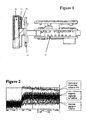
- FIG. 1 shows the schematic setup of the detector according to this embodiment.
- a 6 LiI(Eu) crystal 10 is connected to a semiconductor photo diode 20.
- Neutrons, entering the 6 LiI(Eu) crystal are captured by the 6 Li ions.
- the reaction products, an ⁇ -particle and a tritium particle, are completely stopped in the scintillator crystal 10 thereby generating excited states in that crystal. Those excited states decay with a decay time in the order of 1 ⁇ s.
- the emitted light is then collected by the photo detector 20 which again outputs an electric signal, this signal being directed to the preamplifier 30 and then to an electronic unit 35, this electronic unit 35 being responsible for the sampling and the pulse height and pulse shape analysis of the preamplifier output signals.
- the 6 LiI(Eu) crystal 10 is surrounded by a moderator 15. This moderator 15 slows faster neutrons down to thermal energies so that they could be captured and therefore detected by the 6 LiI(Eu) crystal 10.
- the scintillator crystal 10 also reacts to ⁇ -radiation, being scattered or stopped within the crystal, thus generating scintillation light, being detected by the photo detector 20 also.
- the material used in the scintillator crystal 10 is selected so that the light output, corresponding to the capture of slow (thermal) neutrons is equivalent to the light output, generated by ⁇ -energy measurement with a ⁇ -energy of more than 3 MeV and as, at the same time, ⁇ -radiation, emitted from natural radionuclide sources, has an energy of less than 3 MeV, those two signals can be clearly separated by pulse height analysis.
- the semiconductor photo detector 20 that is the photo diode in the present embodiment, does not stop significant amounts of slow neutrons, but is, as all semiconductor devices, a ⁇ -radiation detector also.
- the photo detector is a photomultiplier, being not sensitive to ⁇ -radiation. Nevertheless, such a photomultiplier is a complex and especially large device, not suitable for handheld detectors.
- the invention as described in this embodiment makes use of the physical effect that the charge collection time in the photo diode 20 is smaller than the light decay time in the scintillator crystal 10. Therefore, the output signals of the photo detector 20 do show a different pulse shape when comparing their timing information.
- the present invention utilizes this effect and distinguishes the neutron induced signals from the scintillator crystal and the ⁇ -induced signals from the photo diode by such a pulse shape analysis.
- the neutron induced signals in the scintillator and the ⁇ -induced signals in the scintillator can be distinguished by pulse height analysis, all three types of signals can be distinguished when combining pulse height and pulse shape analysis.
- Pulse shape analysis can be done in analog and digital electronics. As such a pulse shape analysis in analog electronics is fairly complicated, therefore leading to complicated and expensive devices within the detector, the embodiment provides a signal sampling device, digitizing the output signal of the photo detector.
- the further evaluation of the resulting sampled digital signal is then done with a digital signal processing device, capable of performing such a pulse shape analysis.
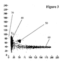
- FIG. 3 A two-dimensional plot, showing the output signals after pulse shape analysis, is shown in Figure 3 .
- the x-axis depicts the energy of the measured signals, whereas the ⁇ -axis is a measure for the pulse shape.
- the neutron induced signals 50 can be clearly distinguished from the ⁇ -induced signals 40 from the scintillator, the ⁇ -induced signals in the photo diode 60 and the background noise 70.
- the detector according to the invention combines pulse height and pulse shape analysis for those signals, thereby allowing for discrimination of both, ⁇ -induced signals 40 from the scintillator and ⁇ -induced signals from the photo diode 60.
- the detector according to the present embodiment has to be calibrated before using it for the first time, including setting a window on the signals, resulting from ⁇ -radiation absorbed by the photo diode, discriminating against those signals.
- the resulting spectrum then only contains signals, produced by light emitted from the scintillator crystal 10, that is signals resulting from ⁇ - and neutron radiation absorbed in said crystal.
- the then resulting signal contains neutron induced signals only, after all ⁇ -induced signals from the photo diode 60 have been discriminated.
- the inventive combination of a suitable scintillator crystal with a semiconductor photo detector for example a photo diode or an avalanche photo diode or the like, in combination with a sampling device and a digital electronics, being capable of performing a pulse height and a pulse shape analysis, results in a very small, compact and robust detector for neutron detection.
- a semiconductor photo detector for example a photo diode or an avalanche photo diode or the like
- the detector according to this invention is a significant step in the direction of further miniaturization and variability of handheld radio isotope identification devices.
Landscapes
- Physics & Mathematics (AREA)
- Health & Medical Sciences (AREA)
- Life Sciences & Earth Sciences (AREA)
- General Physics & Mathematics (AREA)
- High Energy & Nuclear Physics (AREA)
- Molecular Biology (AREA)
- Spectroscopy & Molecular Physics (AREA)
- Measurement Of Radiation (AREA)
- Superconductors And Manufacturing Methods Therefor (AREA)
- Measuring Fluid Pressure (AREA)
- Measuring Instrument Details And Bridges, And Automatic Balancing Devices (AREA)
Abstract
Description
- The invention relates to a solid state neutron detector for detection of neutrons in fields with significant γ-, including x-ray and/or β-radiation.
- The measurement and counting of neutrons is a highly significant problem. Neutrons are for example emitted by special nuclear materials like reactor and/or weapons grade plutonium whereas such materials often do not emit other radiation which can penetrate thick shieldings. Therefore, neutron detection may provide indications or even evidence for the presence of such nuclear materials.
- According to ANSI standards, handheld devices for nuclide identification, which are for example used at boarder crossings, are required to comprise a neutron detector. Measurement of neutrons is further of importance in dosimetry, performed in laboratories and nuclear facilities.
- As neutrons do not ionize matter, all known neutron detectors are based on reactions between a neutron and another nuclide, thereby generating secondary charged particles or γ-radiation. Therefore the standard detection process typically consists of two steps: neutron conversion, that is the generation of secondary radiation in a converter medium, for example by neutrons scattering or neutron induced reactions like nuclear fission, direct nuclear reactions, neutron capture followed by γ- or charged particle emissions or the like. Afterwards, this secondary radiation is measured with usual nuclear radiation detectors in a 'detection medium'.
- In order to detect neutrons, both processes can be spatially separated, that is converter and detection media are different, or not, namely when the converter medium is the detection medium at the same time.
- The detection medium is necessarily sensitive to ionizing radiation. Therefore, if neutrons must be detected in mixed fields, for example in an environment with elevated γ-radiation, the discrimination of neutron against other signals is of major importance. Therefore, neutron detectors in handheld isotope identification devices must not detect γ-radiation from any radionuclide which may be present. Even in the case of strong γ-source, the γ-radiation must not generate false neutron alarms.
- From
US20050127300 Al a radiation detector is known, being able to detect many different types of radiations and intensities. The radiation detector is using a scintillator and a photodiode for detecting radiation. - The most common thermal neutron detector applied almost wherever robustness is an issue, is a proportional counter filled with 3He gas. 3He is at the same time the converter and the detection medium.
- A big disadvantage of such kind of detectors is the neutron detection efficiency. This is approximately proportional to the product of volume and gas pressure. Therefore, such a detector either has to have a large volume or the gas has to be stored under high pressure. As a consequence, the detector can either not be utilized in handheld identification devices because of its large volume or the transportability of such a handheld device is limited, as high pressure devices may be subject to transport regulations like in airplane transportation.
- As a matter of principle, neutron detectors with solid converter media are more appropriate when considering the detection efficiency per volume, at the same time not encountering any problems with high pressure gas devices. Such solid media detectors are often scintillator crystals, comprising lithium (6Li), cadmium (Cd), Boron (10B) or other neutron converters. Such a scintillator crystal is called "neutron scintillator". Such a neutron scintillator is for example 6LiI(Eu), as described in Knoll, Radiation Detection and Measurement, 3rd Edition 2000, page 517.
- In such a crystal, the 6Li captures the thermal neutron, thereby generating a tritium (3H) ion and an α-particle with a combined energy of roughly 4.8 MeV. Due to the relatively low quenching of this 6LiI(Eu) crystal, the light signals following neutrons capture correspond to signals which would be generated by γ-radiation with an energy of more than 3 MeV.
- As all relevant radionuclides do not emit γ-radiation with such high energies, the light signals, being emitted from the 6LiI(Eu) scintillator crystal can be separated by energy discrimination.
- The disadvantage of this prior art is that those detectors have to be used in combination with photomultipliers as light detectors. Other light detectors, namely semiconductor based photo detectors, are sensitive for γ-radiation also, thus acting as γ-detectors themselves generating a much larger signal per unit of deposited γ-energy as in comparison with neutron hits in the scintillator. This is due to the fact that the γ-energy deposed in the scintillator is first translated in a light pulse, only within in a second step generating photo electrons in the semiconductor based photo detector.
- As a consequence, a pulse height analysis may be able to distinguish the neutron capture signals from the γ-hits in the scintillator, but not between neutron capture signals in the scintillator from γ- or x-ray hits with much lower energy directly deposed in the semiconductor based photo detector.
- Therefore, such a detector could only be used for the detection of neutrons in a surrounding, where more or less no γ-radiation is present. As such surroundings are, at least outside a laboratory, not the surroundings which are of some practical relevance, this is not an option.
- It is therefore the object of the invention to provide a very compact neutron detector avoiding the disadvantages of the prior art, especially avoiding having to make use of a high pressure gas device. This problem is solved by a neutron detector according to claim 1. Preferred embodiments are disclosed in the dependent claims.
- The invention provides a neutron detector for detection of neutrons in fields with significant γ-or β-radiation, comprising a neutron sensitive scintillator crystal, providing a neutron capture signal being larger than the capture signal of 3 MeV γ-radiation. In addition, it comprises a semiconductor based photo detector being optically coupled to the scintillator crystal, where the scintillator crystal and the semiconductor based photo detector are selected so that the total charge collection time for scintillator signals in the semiconductor based photo detector is large than the total charge collection time for signals generated by direct detection of ionizing radiation in the semiconductor based photo detector.
- The total charge collection time here means the time which is needed to collect all charge carriers forming the detector signal at the collecting electrode of the photo detector, measured from the onset of the signal (first charge carriers arrive at the collecting electrode).
- This total charge collection time corresponds to the rise time of a charge signal, or the length of the current signal measured at the collecting electrode. In case of direct interactions of ionizing radiation with the photo detector material the total charge collection time is defined only by the drift paths and the drift velocities of charge carriers in the semiconductor, and the geometry of the charge collecting electrode. The initial spatial distribution of generated charge carriers corresponds to an ionization track.
- In case of scintillator signals the charge carriers are generated as photo electrons, located close to the surface of the photo detector and distributed over the full area exposed to the scintillator light. The charge collection time may be very different from that of an ionization track, in particular if the photo detector is a Silicon Drift Detector (SDD). Here, the spatial spread of the photoelectrons is reflected in a spread of arrival times at the collecting electrode which is much larger than that of the localized charge corresponding to an ionization track.
- Furthermore, the duration of the light pulse of the scintillator, given by the light decay, may contribute significantly to the total charge collection time. The total charge collection time is then defined by a combination of both effects.
- Examples of such arrangements are a scintillator with a light decay time larger than the typical charge collection time in a photo diode (PD) or avalanche photo diode (APD), coupled to a PD or APD.
- An alternative is to use a scintillator with either a long or a short light decay time coupled to a Silicon Drift Detector (SDD), as the SDD has a relatively short total charge collection time for the charge tracks generated by ionizing radiation in the Silicon but a much larger total charge collection time for the dispersed cloud of photoelectrons due to a scintillation event.
- Furthermore, there is a device for sampling the detector signals and a digital signal processing device available, as well as means adapted to distinguish direct signals from the semiconductor based photo detector, caused by γ- or β-radiation and being at least partially absorbed in the semiconductor based photo detector, from light signals entering the semiconductor based photo detector, after being emitted from the scintillator crystal after capturing at least one neutron, by means of pulse shape discrimination, utilizing a difference between the total charge collection time for scintillator signals from the total charge collection time for signals generated by direct detection of ionizing radiation in the semiconductor based photo detector. The detector also comprises means adapted to distinguish neutron induced signals from γ- or β-radiation induced signals in the scintillator crystal by discriminating the different signals via their pulse height, making use of the difference between the number of photons generated by neutron and γ-radiation in the field of interest.
- In a preferred embodiment, the semiconductor based photo detector is selected from a group of detectors, comprising a Photo Diode (PD), an Avalanche Photo Diode (APD) and a Silicon Drift Detector (SDD).
- It has proven advantageous, if the light decay time of the scintillation crystal is larger than 100 ns, for example by using a scintillation crystal comprising 6LiI(Eu).
- It is possible to utilize a scintillation crystal which is smaller than 2 cm3, preferably smaller than 0.5 cm3.
- When other than thermal neutrons are to be detected with the inventive detector, it is an advantage to use a a surrounding neutron moderating medium, slowing down the fast neutrons, so that mainly thermal neutrons enter the scintillation crystal.
- The invention also provides for a complete detector system, comprising a neutron detector as described in combination with sampling electronics and a computer program, capable of evaluating the measured and sampled data, especially being capable of performing a pulse shape analysis of said data.
- It is even more preferable to combine such a neutron detector, which can be realized in a very tiny setup, with other radiation detectors, for example with a γ-detector designed for spectroscopy. Such a combined detector is especially useful for the purposes of homeland security, as it can be used as handheld radioisotope identifier.
- It is even possible to exploit the neutron detector provided by the invention as a γ-detector, since the scintillator detects γ radiation as well.
- A specific example of the invention is described in the following:
- Figure 1
- shows the principle setup of a detector,
- Figure 2
- shows signals measured by such a detector,
- Figure 3
- shows a two-dimensional spectrum utilizing pulse shape discrimi- nation of the signals.
-
Figure 1 shows the schematic setup of the detector according to this embodiment. A 6LiI(Eu)crystal 10 is connected to asemiconductor photo diode 20. Neutrons, entering the 6LiI(Eu) crystal, are captured by the 6Li ions. The reaction products, an α-particle and a tritium particle, are completely stopped in thescintillator crystal 10 thereby generating excited states in that crystal. Those excited states decay with a decay time in the order of 1µs. - The emitted light is then collected by the
photo detector 20 which again outputs an electric signal, this signal being directed to thepreamplifier 30 and then to anelectronic unit 35, thiselectronic unit 35 being responsible for the sampling and the pulse height and pulse shape analysis of the preamplifier output signals. - In order to allow for the detection of other than thermal neutrons, the 6LiI(Eu)
crystal 10 is surrounded by amoderator 15. Thismoderator 15 slows faster neutrons down to thermal energies so that they could be captured and therefore detected by the 6LiI(Eu)crystal 10. - The
scintillator crystal 10 also reacts to γ-radiation, being scattered or stopped within the crystal, thus generating scintillation light, being detected by thephoto detector 20 also. - As the material used in the
scintillator crystal 10 is selected so that the light output, corresponding to the capture of slow (thermal) neutrons is equivalent to the light output, generated by γ-energy measurement with a γ-energy of more than 3 MeV and as, at the same time, γ-radiation, emitted from natural radionuclide sources, has an energy of less than 3 MeV, those two signals can be clearly separated by pulse height analysis. - The γ-signal in 6LiI(Eu), which can be seen in
Figure 2 , can be clearly distinguished from the neutron capture signal in 6LiI(Eu) by its energy. - The
semiconductor photo detector 20, that is the photo diode in the present embodiment, does not stop significant amounts of slow neutrons, but is, as all semiconductor devices, a γ-radiation detector also. The signals resulting from those γ-radiation, interacting with thephoto diode 20 directly, are shown inFigure 2 also. Even if they generally seem to have a higher energy as the captured neutron signals, they nevertheless do produce a significant noise with regard to the neutron capture signals 50. This can be seen from the spectrum ofFigure 3 , discussed bellow. - To meet the ANSI and other (e.g. IAEA) standards for neutron sensitivity in handheld radionuclide identification devices it is necessary to derive neutron alarms from single neutron counts, e.g. if two neutrons are detected within a time period of 5 seconds. Therefore, a secure and robust detection of neutrons and therefore a save distinguishing of neutron signals from background is required.
- In detectors as known from the state of the art, the photo detector is a photomultiplier, being not sensitive to γ-radiation. Nevertheless, such a photomultiplier is a complex and especially large device, not suitable for handheld detectors.
- The invention as described in this embodiment makes use of the physical effect that the charge collection time in the
photo diode 20 is smaller than the light decay time in thescintillator crystal 10. Therefore, the output signals of thephoto detector 20 do show a different pulse shape when comparing their timing information. - The present invention utilizes this effect and distinguishes the neutron induced signals from the scintillator crystal and the γ-induced signals from the photo diode by such a pulse shape analysis. As, at the same time, the neutron induced signals in the scintillator and the γ-induced signals in the scintillator can be distinguished by pulse height analysis, all three types of signals can be distinguished when combining pulse height and pulse shape analysis.
- Pulse shape analysis can be done in analog and digital electronics. As such a pulse shape analysis in analog electronics is fairly complicated, therefore leading to complicated and expensive devices within the detector, the embodiment provides a signal sampling device, digitizing the output signal of the photo detector.
- The further evaluation of the resulting sampled digital signal is then done with a digital signal processing device, capable of performing such a pulse shape analysis.
- A two-dimensional plot, showing the output signals after pulse shape analysis, is shown in
Figure 3 . - The x-axis depicts the energy of the measured signals, whereas the γ-axis is a measure for the pulse shape. The neutron induced signals 50 can be clearly distinguished from the γ-induced
signals 40 from the scintillator, the γ-induced signals in thephoto diode 60 and thebackground noise 70. - As mentioned above already, the γ-induced signals in the
photo diode 60 generally seem to have a higher energy than the neutron inducedsignals 50, but still a significant number of signals of the γ-induced signals in thephoto diode 60 seem to have the same energy then the neutron induced signals 50. As the above cited ANSI standard does require the robust detection of single neutrons, such a γ-noise is not acceptable for respective devices. Therefore, the detector according to the invention combines pulse height and pulse shape analysis for those signals, thereby allowing for discrimination of both, γ-inducedsignals 40 from the scintillator and γ-induced signals from thephoto diode 60. - The detector according to the present embodiment has to be calibrated before using it for the first time, including setting a window on the signals, resulting from γ-radiation absorbed by the photo diode, discriminating against those signals. The resulting spectrum then only contains signals, produced by light emitted from the
scintillator crystal 10, that is signals resulting from γ- and neutron radiation absorbed in said crystal. - Setting a pulse height window on the
neutron spot 50 inFigure 3 , the then resulting signal contains neutron induced signals only, after all γ-induced signals from thephoto diode 60 have been discriminated. - As a result, the inventive combination of a suitable scintillator crystal with a semiconductor photo detector, for example a photo diode or an avalanche photo diode or the like, in combination with a sampling device and a digital electronics, being capable of performing a pulse height and a pulse shape analysis, results in a very small, compact and robust detector for neutron detection. As this detector does not contain gas under pressure, it can easily be transported in airplanes also.
- Experiments have shown that a 6LiI(Eu) crystal with a volume less than ½ ccm is sufficient to comply with the ANSI standards for the detection of slow neutrons. Therefore, the detector according to this invention is a significant step in the direction of further miniaturization and variability of handheld radio isotope identification devices.
Claims (7)
- Neutron detector for detection of neutrons in fields with significant γ-or β- radiation, comprising• a neutron sensitive scintillator crystal (10), providing a neutron capture signal being larger than the capture signal of 3 MeV γ-radiation,• a semiconductor based photo detector (20) being optically coupled to the scintillator crystal (10), where the scintillator crystal (10) and the semiconductor based photo detector (20) are selected so that the total charge collection time for scintillator signals in the semiconductor based photo detector is larger than the total charge collection time for signals generated by direct detection of ionizing radiation in the semiconductor based photo detector,• a device (35) for sampling the detector signals,• a digital signal processing device,• means adapted to distinguish direct signals from the semiconductor based photo detector (20), caused by γ- or β-radiation and being at least partially absorbed in the semiconductor based photo detector (20), from light signals entering the semiconductor based photo detector, after being emitted from the scintillator crystal (10) after capturing at least one neutron, by means of pulse shape discrimination, utilizing a difference between the total charge collection time for scintillator signals from the total charge collection time for signals generated by direct detection of ionizing radiation in the semiconductor based photo detector (20),• means adapted to distinguish neutron induced signals (50) from γ-radiation induced signals (40) in the scintillator crystal by discriminating the different signals via their pulse height, making use of the difference between the number of photons generated by neutron and γ-radiation in the field of interest.
- Neutron detector according to claim 1, characterized in that the semiconductor based photo detector is a Silicon Drift Detector (SDD).
- Neutron detector according to claim 1, characterized in that the light decay time of the scintillation crystal is larger than 100 ns.
- Neutron detector according to claim 1, characterized in that the scintillation crystal comprises 6LiI(Eu).
- Neutron detector according to claim 1, characterized in that the semiconductor based photo detector is selected from a group of detectors, comprising a Photo Diode (PD) and an Avalanche Photo Diode (APD).
- Neutron detector according to claim 1, characterized in that the scintillation crystal is smaller than 2 cm3, preferably smaller than 0.5 cm3.
- Neutron detector according to one of the preceding claims with a surrounding neutron moderating medium.
Applications Claiming Priority (1)
| Application Number | Priority Date | Filing Date | Title |
|---|---|---|---|
| PCT/EP2007/052063 WO2008107017A1 (en) | 2007-03-05 | 2007-03-05 | Solid state neutron detector |
Publications (2)
| Publication Number | Publication Date |
|---|---|
| EP1989573A1 EP1989573A1 (en) | 2008-11-12 |
| EP1989573B1 true EP1989573B1 (en) | 2011-03-02 |
Family
ID=38983232
Family Applications (1)
| Application Number | Title | Priority Date | Filing Date |
|---|---|---|---|
| EP07712448A Not-in-force EP1989573B1 (en) | 2007-03-05 | 2007-03-05 | Solid state neutron detector |
Country Status (6)
| Country | Link |
|---|---|
| US (1) | US8232530B2 (en) |
| EP (1) | EP1989573B1 (en) |
| AT (1) | ATE500524T1 (en) |
| DE (1) | DE602007012839D1 (en) |
| IL (1) | IL200703A0 (en) |
| WO (1) | WO2008107017A1 (en) |
Families Citing this family (9)
| Publication number | Priority date | Publication date | Assignee | Title |
|---|---|---|---|---|
| US8153985B2 (en) | 2009-01-30 | 2012-04-10 | Honeywell International Inc. | Neutron detector cell efficiency |
| WO2011145651A1 (en) * | 2010-05-18 | 2011-11-24 | 株式会社トクヤマ | Neutron beam detector, neutron beam detection scintillator, and method for discrimination between neutron beam and γ beam |
| US8310021B2 (en) | 2010-07-13 | 2012-11-13 | Honeywell International Inc. | Neutron detector with wafer-to-wafer bonding |
| US8884234B2 (en) * | 2012-03-16 | 2014-11-11 | Raytheon Company | Portable directional device for locating neutron emitting sources |
| US9804290B2 (en) * | 2013-04-02 | 2017-10-31 | Morpho Detection, Llc | Cross-correlated gamma ray and neutron detector |
| US10191161B1 (en) | 2017-03-30 | 2019-01-29 | Consolidated Nuclear Security, LLC | Device and method for the location and identification of a radiation source |
| CN109143318B (en) * | 2017-06-16 | 2023-09-15 | 中国辐射防护研究院 | Neutron detection method and equipment for reducing gamma ray interference by using silicon PIN detector |
| CN110136860B (en) * | 2019-05-25 | 2024-08-27 | 广东太微加速器有限公司 | Fast neutron screening device and screening method |
| WO2021011395A1 (en) | 2019-07-16 | 2021-01-21 | Georgia Tech Research Corporation | Electrical resistance device for radiation detection |
Family Cites Families (8)
| Publication number | Priority date | Publication date | Assignee | Title |
|---|---|---|---|---|
| US3566118A (en) * | 1968-11-14 | 1971-02-23 | Us Navy | An axially aligned gamma ray-neutron detector |
| US5446288A (en) * | 1993-10-25 | 1995-08-29 | Tumer; Tumay O. | Integrated substance detection instrument |
| RU2082156C1 (en) | 1994-06-01 | 1997-06-20 | Физический институт им.П.Н.Лебедева РАН | Method for detection of fission materials |
| RU2119178C1 (en) | 1997-04-25 | 1998-09-20 | Тарабрин Юрий Александрович | Neutron detector |
| US5936246A (en) | 1997-07-22 | 1999-08-10 | S. E. International, Inc. | Portable radiation detector |
| US7115872B2 (en) * | 2003-12-10 | 2006-10-03 | John William Bordynuik | Portable radiation detector and method of detecting radiation |
| EP1553430A1 (en) * | 2004-01-09 | 2005-07-13 | Stichting Voor De Technische Wetenschappen | High light yield thermal neutron scintillators |
| US7635848B2 (en) * | 2005-04-01 | 2009-12-22 | San Diego State University Research Foundation | Edge-on SAR scintillator devices and systems for enhanced SPECT, PET, and compton gamma cameras |
-
2007
- 2007-03-05 DE DE602007012839T patent/DE602007012839D1/en active Active
- 2007-03-05 AT AT07712448T patent/ATE500524T1/en not_active IP Right Cessation
- 2007-03-05 EP EP07712448A patent/EP1989573B1/en not_active Not-in-force
- 2007-03-05 US US12/067,903 patent/US8232530B2/en not_active Expired - Fee Related
- 2007-03-05 WO PCT/EP2007/052063 patent/WO2008107017A1/en not_active Ceased
-
2009
- 2009-09-03 IL IL200703A patent/IL200703A0/en unknown
Also Published As
| Publication number | Publication date |
|---|---|
| WO2008107017A1 (en) | 2008-09-12 |
| US20100181488A1 (en) | 2010-07-22 |
| IL200703A0 (en) | 2010-05-17 |
| US8232530B2 (en) | 2012-07-31 |
| ATE500524T1 (en) | 2011-03-15 |
| EP1989573A1 (en) | 2008-11-12 |
| DE602007012839D1 (en) | 2011-04-14 |
Similar Documents
| Publication | Publication Date | Title |
|---|---|---|
| US7288771B2 (en) | Fiber optic thermal/fast neutron and gamma ray scintillation detector | |
| US8232530B2 (en) | Solid state neutron detector | |
| US7388206B2 (en) | Pulse shape discrimination method and apparatus for high-sensitivity radioisotope identification with an integrated neutron-gamma radiation detector | |
| US6876711B2 (en) | Neutron detector utilizing sol-gel absorber and activation disk | |
| EP2517050B1 (en) | Composite gamma-neutron detection system | |
| EP3066496B1 (en) | Device and method for detecting neutrons and gamma rays | |
| US20050105665A1 (en) | Detection of neutrons and sources of radioactive material | |
| US11163076B2 (en) | Method for the detection of neutrons with scintillation detectors used for gamma ray spectroscopy | |
| US7877340B2 (en) | System and method for resolving gamma-ray spectra | |
| Streicher et al. | Special nuclear material characterization using digital 3-D position sensitive CdZnTe detectors and high purity germanium spectrometers | |
| RU2143711C1 (en) | Detector for registration of ionizing radiation | |
| Yang et al. | Fusion of X-ray imaging and photoneutron induced gamma analysis for contrabands detection | |
| US20230400597A1 (en) | Neutron counting by delayed capture-gamma detection (dcd) | |
| US10191161B1 (en) | Device and method for the location and identification of a radiation source | |
| RU2413246C1 (en) | Solid-state neutron detector | |
| EP4330729A1 (en) | System and method to count neutrons | |
| Trombetta et al. | Investigation of the use of coincidences between fast neutrons and gamma rays for the detection of special nuclear materials | |
| RU2615709C1 (en) | Device for measuring neutron flow density of nuclear power plant in terms of background interference from gamma rays and high-energy space electrons and protons | |
| RU2347241C1 (en) | Detector for recording of ionising radiation | |
| Jones | A novel detection system using neutron/gamma pulse shape discrimination, for use in active interrogation environments | |
| Trombetta et al. | Sensitive detection of special nuclear materials for rpm applications based on gamma-fast neutron coincidence counting | |
| Zimmerman et al. | Optimized system for hydrogen detection | |
| Geist et al. | Evaluation of a fast neutron coincidence counter for the measurements of uranium samples | |
| Corre et al. | Neutron detection with large plastic scintillators for RPM applications | |
| Jensen et al. | High-efficiency fast-neutron detectors |
Legal Events
| Date | Code | Title | Description |
|---|---|---|---|
| PUAI | Public reference made under article 153(3) epc to a published international application that has entered the european phase |
Free format text: ORIGINAL CODE: 0009012 |
|
| 17P | Request for examination filed |
Effective date: 20080305 |
|
| AK | Designated contracting states |
Kind code of ref document: A1 Designated state(s): AT BE BG CH CY CZ DE DK EE ES FI FR GB GR HU IE IS IT LI LT LU LV MC MT NL PL PT RO SE SI SK TR |
|
| AX | Request for extension of the european patent |
Extension state: AL BA HR MK RS |
|
| 17Q | First examination report despatched |
Effective date: 20090409 |
|
| RAP1 | Party data changed (applicant data changed or rights of an application transferred) |
Owner name: ICX TECHNOLOGIES GMBH |
|
| GRAP | Despatch of communication of intention to grant a patent |
Free format text: ORIGINAL CODE: EPIDOSNIGR1 |
|
| DAX | Request for extension of the european patent (deleted) | ||
| GRAS | Grant fee paid |
Free format text: ORIGINAL CODE: EPIDOSNIGR3 |
|
| GRAA | (expected) grant |
Free format text: ORIGINAL CODE: 0009210 |
|
| AK | Designated contracting states |
Kind code of ref document: B1 Designated state(s): AT BE BG CH CY CZ DE DK EE ES FI FR GB GR HU IE IS IT LI LT LU LV MC MT NL PL PT RO SE SI SK TR |
|
| REG | Reference to a national code |
Ref country code: GB Ref legal event code: FG4D |
|
| REG | Reference to a national code |
Ref country code: CH Ref legal event code: EP |
|
| REG | Reference to a national code |
Ref country code: IE Ref legal event code: FG4D |
|
| REF | Corresponds to: |
Ref document number: 602007012839 Country of ref document: DE Date of ref document: 20110414 Kind code of ref document: P |
|
| REG | Reference to a national code |
Ref country code: DE Ref legal event code: R096 Ref document number: 602007012839 Country of ref document: DE Effective date: 20110414 |
|
| REG | Reference to a national code |
Ref country code: NL Ref legal event code: VDEP Effective date: 20110302 |
|
| PG25 | Lapsed in a contracting state [announced via postgrant information from national office to epo] |
Ref country code: GR Free format text: LAPSE BECAUSE OF FAILURE TO SUBMIT A TRANSLATION OF THE DESCRIPTION OR TO PAY THE FEE WITHIN THE PRESCRIBED TIME-LIMIT Effective date: 20110603 Ref country code: LT Free format text: LAPSE BECAUSE OF FAILURE TO SUBMIT A TRANSLATION OF THE DESCRIPTION OR TO PAY THE FEE WITHIN THE PRESCRIBED TIME-LIMIT Effective date: 20110302 Ref country code: ES Free format text: LAPSE BECAUSE OF FAILURE TO SUBMIT A TRANSLATION OF THE DESCRIPTION OR TO PAY THE FEE WITHIN THE PRESCRIBED TIME-LIMIT Effective date: 20110613 Ref country code: SE Free format text: LAPSE BECAUSE OF FAILURE TO SUBMIT A TRANSLATION OF THE DESCRIPTION OR TO PAY THE FEE WITHIN THE PRESCRIBED TIME-LIMIT Effective date: 20110302 Ref country code: LV Free format text: LAPSE BECAUSE OF FAILURE TO SUBMIT A TRANSLATION OF THE DESCRIPTION OR TO PAY THE FEE WITHIN THE PRESCRIBED TIME-LIMIT Effective date: 20110302 |
|
| LTIE | Lt: invalidation of european patent or patent extension |
Effective date: 20110302 |
|
| PG25 | Lapsed in a contracting state [announced via postgrant information from national office to epo] |
Ref country code: SI Free format text: LAPSE BECAUSE OF FAILURE TO SUBMIT A TRANSLATION OF THE DESCRIPTION OR TO PAY THE FEE WITHIN THE PRESCRIBED TIME-LIMIT Effective date: 20110302 Ref country code: CY Free format text: LAPSE BECAUSE OF FAILURE TO SUBMIT A TRANSLATION OF THE DESCRIPTION OR TO PAY THE FEE WITHIN THE PRESCRIBED TIME-LIMIT Effective date: 20110302 Ref country code: AT Free format text: LAPSE BECAUSE OF FAILURE TO SUBMIT A TRANSLATION OF THE DESCRIPTION OR TO PAY THE FEE WITHIN THE PRESCRIBED TIME-LIMIT Effective date: 20110302 Ref country code: BG Free format text: LAPSE BECAUSE OF FAILURE TO SUBMIT A TRANSLATION OF THE DESCRIPTION OR TO PAY THE FEE WITHIN THE PRESCRIBED TIME-LIMIT Effective date: 20110602 Ref country code: NL Free format text: LAPSE BECAUSE OF FAILURE TO SUBMIT A TRANSLATION OF THE DESCRIPTION OR TO PAY THE FEE WITHIN THE PRESCRIBED TIME-LIMIT Effective date: 20110302 Ref country code: FI Free format text: LAPSE BECAUSE OF FAILURE TO SUBMIT A TRANSLATION OF THE DESCRIPTION OR TO PAY THE FEE WITHIN THE PRESCRIBED TIME-LIMIT Effective date: 20110302 |
|
| PG25 | Lapsed in a contracting state [announced via postgrant information from national office to epo] |
Ref country code: BE Free format text: LAPSE BECAUSE OF FAILURE TO SUBMIT A TRANSLATION OF THE DESCRIPTION OR TO PAY THE FEE WITHIN THE PRESCRIBED TIME-LIMIT Effective date: 20110302 |
|
| PG25 | Lapsed in a contracting state [announced via postgrant information from national office to epo] |
Ref country code: EE Free format text: LAPSE BECAUSE OF FAILURE TO SUBMIT A TRANSLATION OF THE DESCRIPTION OR TO PAY THE FEE WITHIN THE PRESCRIBED TIME-LIMIT Effective date: 20110302 Ref country code: MC Free format text: LAPSE BECAUSE OF NON-PAYMENT OF DUE FEES Effective date: 20110331 Ref country code: PT Free format text: LAPSE BECAUSE OF FAILURE TO SUBMIT A TRANSLATION OF THE DESCRIPTION OR TO PAY THE FEE WITHIN THE PRESCRIBED TIME-LIMIT Effective date: 20110704 |
|
| REG | Reference to a national code |
Ref country code: CH Ref legal event code: PL |
|
| PG25 | Lapsed in a contracting state [announced via postgrant information from national office to epo] |
Ref country code: CZ Free format text: LAPSE BECAUSE OF FAILURE TO SUBMIT A TRANSLATION OF THE DESCRIPTION OR TO PAY THE FEE WITHIN THE PRESCRIBED TIME-LIMIT Effective date: 20110302 Ref country code: SK Free format text: LAPSE BECAUSE OF FAILURE TO SUBMIT A TRANSLATION OF THE DESCRIPTION OR TO PAY THE FEE WITHIN THE PRESCRIBED TIME-LIMIT Effective date: 20110302 Ref country code: IS Free format text: LAPSE BECAUSE OF FAILURE TO SUBMIT A TRANSLATION OF THE DESCRIPTION OR TO PAY THE FEE WITHIN THE PRESCRIBED TIME-LIMIT Effective date: 20110702 Ref country code: RO Free format text: LAPSE BECAUSE OF FAILURE TO SUBMIT A TRANSLATION OF THE DESCRIPTION OR TO PAY THE FEE WITHIN THE PRESCRIBED TIME-LIMIT Effective date: 20110302 |
|
| PG25 | Lapsed in a contracting state [announced via postgrant information from national office to epo] |
Ref country code: MT Free format text: LAPSE BECAUSE OF FAILURE TO SUBMIT A TRANSLATION OF THE DESCRIPTION OR TO PAY THE FEE WITHIN THE PRESCRIBED TIME-LIMIT Effective date: 20110302 |
|
| REG | Reference to a national code |
Ref country code: IE Ref legal event code: MM4A |
|
| PLBE | No opposition filed within time limit |
Free format text: ORIGINAL CODE: 0009261 |
|
| STAA | Information on the status of an ep patent application or granted ep patent |
Free format text: STATUS: NO OPPOSITION FILED WITHIN TIME LIMIT |
|
| PG25 | Lapsed in a contracting state [announced via postgrant information from national office to epo] |
Ref country code: IE Free format text: LAPSE BECAUSE OF NON-PAYMENT OF DUE FEES Effective date: 20110305 Ref country code: CH Free format text: LAPSE BECAUSE OF NON-PAYMENT OF DUE FEES Effective date: 20110331 Ref country code: LI Free format text: LAPSE BECAUSE OF NON-PAYMENT OF DUE FEES Effective date: 20110331 |
|
| 26N | No opposition filed |
Effective date: 20111205 |
|
| PG25 | Lapsed in a contracting state [announced via postgrant information from national office to epo] |
Ref country code: PL Free format text: LAPSE BECAUSE OF FAILURE TO SUBMIT A TRANSLATION OF THE DESCRIPTION OR TO PAY THE FEE WITHIN THE PRESCRIBED TIME-LIMIT Effective date: 20110302 Ref country code: DK Free format text: LAPSE BECAUSE OF FAILURE TO SUBMIT A TRANSLATION OF THE DESCRIPTION OR TO PAY THE FEE WITHIN THE PRESCRIBED TIME-LIMIT Effective date: 20110302 |
|
| REG | Reference to a national code |
Ref country code: DE Ref legal event code: R097 Ref document number: 602007012839 Country of ref document: DE Effective date: 20111205 |
|
| PG25 | Lapsed in a contracting state [announced via postgrant information from national office to epo] |
Ref country code: IT Free format text: LAPSE BECAUSE OF FAILURE TO SUBMIT A TRANSLATION OF THE DESCRIPTION OR TO PAY THE FEE WITHIN THE PRESCRIBED TIME-LIMIT Effective date: 20110302 |
|
| PGFP | Annual fee paid to national office [announced via postgrant information from national office to epo] |
Ref country code: FR Payment date: 20130329 Year of fee payment: 7 Ref country code: GB Payment date: 20130318 Year of fee payment: 7 Ref country code: DE Payment date: 20130320 Year of fee payment: 7 |
|
| PG25 | Lapsed in a contracting state [announced via postgrant information from national office to epo] |
Ref country code: LU Free format text: LAPSE BECAUSE OF NON-PAYMENT OF DUE FEES Effective date: 20110305 |
|
| PG25 | Lapsed in a contracting state [announced via postgrant information from national office to epo] |
Ref country code: TR Free format text: LAPSE BECAUSE OF FAILURE TO SUBMIT A TRANSLATION OF THE DESCRIPTION OR TO PAY THE FEE WITHIN THE PRESCRIBED TIME-LIMIT Effective date: 20110302 |
|
| PG25 | Lapsed in a contracting state [announced via postgrant information from national office to epo] |
Ref country code: HU Free format text: LAPSE BECAUSE OF FAILURE TO SUBMIT A TRANSLATION OF THE DESCRIPTION OR TO PAY THE FEE WITHIN THE PRESCRIBED TIME-LIMIT Effective date: 20110302 |
|
| REG | Reference to a national code |
Ref country code: DE Ref legal event code: R119 Ref document number: 602007012839 Country of ref document: DE |
|
| GBPC | Gb: european patent ceased through non-payment of renewal fee |
Effective date: 20140305 |
|
| REG | Reference to a national code |
Ref country code: FR Ref legal event code: ST Effective date: 20141128 |
|
| REG | Reference to a national code |
Ref country code: DE Ref legal event code: R119 Ref document number: 602007012839 Country of ref document: DE Effective date: 20141001 |
|
| PG25 | Lapsed in a contracting state [announced via postgrant information from national office to epo] |
Ref country code: GB Free format text: LAPSE BECAUSE OF NON-PAYMENT OF DUE FEES Effective date: 20140305 Ref country code: FR Free format text: LAPSE BECAUSE OF NON-PAYMENT OF DUE FEES Effective date: 20140331 Ref country code: DE Free format text: LAPSE BECAUSE OF NON-PAYMENT OF DUE FEES Effective date: 20141001 |