EP1988628A1 - LC voltage controlled oscillator with tunable capacitance unit - Google Patents
LC voltage controlled oscillator with tunable capacitance unit Download PDFInfo
- Publication number
- EP1988628A1 EP1988628A1 EP07115764A EP07115764A EP1988628A1 EP 1988628 A1 EP1988628 A1 EP 1988628A1 EP 07115764 A EP07115764 A EP 07115764A EP 07115764 A EP07115764 A EP 07115764A EP 1988628 A1 EP1988628 A1 EP 1988628A1
- Authority
- EP
- European Patent Office
- Prior art keywords
- pair
- coupled
- accumulation
- voltage
- mode mos
- Prior art date
- Legal status (The legal status is an assumption and is not a legal conclusion. Google has not performed a legal analysis and makes no representation as to the accuracy of the status listed.)
- Withdrawn
Links
- 239000003990 capacitor Substances 0.000 claims abstract description 23
- 230000000903 blocking effect Effects 0.000 claims abstract description 18
- 238000010586 diagram Methods 0.000 description 24
- 230000008859 change Effects 0.000 description 13
- 238000000034 method Methods 0.000 description 13
- 230000008569 process Effects 0.000 description 13
- 238000004088 simulation Methods 0.000 description 5
- 230000015556 catabolic process Effects 0.000 description 2
- 238000006731 degradation reaction Methods 0.000 description 2
- 229910003460 diamond Inorganic materials 0.000 description 2
- 239000010432 diamond Substances 0.000 description 2
- 230000007246 mechanism Effects 0.000 description 2
- 230000004048 modification Effects 0.000 description 2
- 238000012986 modification Methods 0.000 description 2
- 230000002277 temperature effect Effects 0.000 description 2
- 230000008878 coupling Effects 0.000 description 1
- 238000010168 coupling process Methods 0.000 description 1
- 238000005859 coupling reaction Methods 0.000 description 1
- 230000003071 parasitic effect Effects 0.000 description 1
Images








Classifications
-
- H—ELECTRICITY
- H03—ELECTRONIC CIRCUITRY
- H03B—GENERATION OF OSCILLATIONS, DIRECTLY OR BY FREQUENCY-CHANGING, BY CIRCUITS EMPLOYING ACTIVE ELEMENTS WHICH OPERATE IN A NON-SWITCHING MANNER; GENERATION OF NOISE BY SUCH CIRCUITS
- H03B5/00—Generation of oscillations using amplifier with regenerative feedback from output to input
- H03B5/08—Generation of oscillations using amplifier with regenerative feedback from output to input with frequency-determining element comprising lumped inductance and capacitance
- H03B5/12—Generation of oscillations using amplifier with regenerative feedback from output to input with frequency-determining element comprising lumped inductance and capacitance active element in amplifier being semiconductor device
- H03B5/1228—Generation of oscillations using amplifier with regenerative feedback from output to input with frequency-determining element comprising lumped inductance and capacitance active element in amplifier being semiconductor device the amplifier comprising one or more field effect transistors
-
- H—ELECTRICITY
- H03—ELECTRONIC CIRCUITRY
- H03B—GENERATION OF OSCILLATIONS, DIRECTLY OR BY FREQUENCY-CHANGING, BY CIRCUITS EMPLOYING ACTIVE ELEMENTS WHICH OPERATE IN A NON-SWITCHING MANNER; GENERATION OF NOISE BY SUCH CIRCUITS
- H03B5/00—Generation of oscillations using amplifier with regenerative feedback from output to input
- H03B5/08—Generation of oscillations using amplifier with regenerative feedback from output to input with frequency-determining element comprising lumped inductance and capacitance
- H03B5/12—Generation of oscillations using amplifier with regenerative feedback from output to input with frequency-determining element comprising lumped inductance and capacitance active element in amplifier being semiconductor device
- H03B5/1206—Generation of oscillations using amplifier with regenerative feedback from output to input with frequency-determining element comprising lumped inductance and capacitance active element in amplifier being semiconductor device using multiple transistors for amplification
- H03B5/1212—Generation of oscillations using amplifier with regenerative feedback from output to input with frequency-determining element comprising lumped inductance and capacitance active element in amplifier being semiconductor device using multiple transistors for amplification the amplifier comprising a pair of transistors, wherein an output terminal of each being connected to an input terminal of the other, e.g. a cross coupled pair
-
- H—ELECTRICITY
- H03—ELECTRONIC CIRCUITRY
- H03B—GENERATION OF OSCILLATIONS, DIRECTLY OR BY FREQUENCY-CHANGING, BY CIRCUITS EMPLOYING ACTIVE ELEMENTS WHICH OPERATE IN A NON-SWITCHING MANNER; GENERATION OF NOISE BY SUCH CIRCUITS
- H03B5/00—Generation of oscillations using amplifier with regenerative feedback from output to input
- H03B5/08—Generation of oscillations using amplifier with regenerative feedback from output to input with frequency-determining element comprising lumped inductance and capacitance
- H03B5/12—Generation of oscillations using amplifier with regenerative feedback from output to input with frequency-determining element comprising lumped inductance and capacitance active element in amplifier being semiconductor device
- H03B5/1237—Generation of oscillations using amplifier with regenerative feedback from output to input with frequency-determining element comprising lumped inductance and capacitance active element in amplifier being semiconductor device comprising means for varying the frequency of the generator
- H03B5/124—Generation of oscillations using amplifier with regenerative feedback from output to input with frequency-determining element comprising lumped inductance and capacitance active element in amplifier being semiconductor device comprising means for varying the frequency of the generator the means comprising a voltage dependent capacitance
-
- H—ELECTRICITY
- H03—ELECTRONIC CIRCUITRY
- H03B—GENERATION OF OSCILLATIONS, DIRECTLY OR BY FREQUENCY-CHANGING, BY CIRCUITS EMPLOYING ACTIVE ELEMENTS WHICH OPERATE IN A NON-SWITCHING MANNER; GENERATION OF NOISE BY SUCH CIRCUITS
- H03B5/00—Generation of oscillations using amplifier with regenerative feedback from output to input
- H03B5/08—Generation of oscillations using amplifier with regenerative feedback from output to input with frequency-determining element comprising lumped inductance and capacitance
- H03B5/12—Generation of oscillations using amplifier with regenerative feedback from output to input with frequency-determining element comprising lumped inductance and capacitance active element in amplifier being semiconductor device
- H03B5/1237—Generation of oscillations using amplifier with regenerative feedback from output to input with frequency-determining element comprising lumped inductance and capacitance active element in amplifier being semiconductor device comprising means for varying the frequency of the generator
- H03B5/1262—Generation of oscillations using amplifier with regenerative feedback from output to input with frequency-determining element comprising lumped inductance and capacitance active element in amplifier being semiconductor device comprising means for varying the frequency of the generator the means comprising switched elements
- H03B5/1265—Generation of oscillations using amplifier with regenerative feedback from output to input with frequency-determining element comprising lumped inductance and capacitance active element in amplifier being semiconductor device comprising means for varying the frequency of the generator the means comprising switched elements switched capacitors
-
- H—ELECTRICITY
- H03—ELECTRONIC CIRCUITRY
- H03B—GENERATION OF OSCILLATIONS, DIRECTLY OR BY FREQUENCY-CHANGING, BY CIRCUITS EMPLOYING ACTIVE ELEMENTS WHICH OPERATE IN A NON-SWITCHING MANNER; GENERATION OF NOISE BY SUCH CIRCUITS
- H03B5/00—Generation of oscillations using amplifier with regenerative feedback from output to input
- H03B5/08—Generation of oscillations using amplifier with regenerative feedback from output to input with frequency-determining element comprising lumped inductance and capacitance
- H03B5/12—Generation of oscillations using amplifier with regenerative feedback from output to input with frequency-determining element comprising lumped inductance and capacitance active element in amplifier being semiconductor device
- H03B5/1237—Generation of oscillations using amplifier with regenerative feedback from output to input with frequency-determining element comprising lumped inductance and capacitance active element in amplifier being semiconductor device comprising means for varying the frequency of the generator
- H03B5/1293—Generation of oscillations using amplifier with regenerative feedback from output to input with frequency-determining element comprising lumped inductance and capacitance active element in amplifier being semiconductor device comprising means for varying the frequency of the generator having means for achieving a desired tuning characteristic, e.g. linearising the frequency characteristic across the tuning voltage range
Definitions
- the invention relates to a voltage controlled oscillator (VCO) and, in particular, to an LC VCO with a tunable capacitance unit.
- VCO voltage controlled oscillator
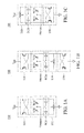
- Figs 1A, 1B and 1C are respectively a circuit diagram of a LC tank voltage controlled oscillator (VCO) 100, or an LC VCO.
- the LC VCO 100 typically comprises an LC tank circuit 110 and a negative resistance circuit 120.
- the LC tank circuit 110 comprises an inductor L and a tunable capacitance unit TCU.
- a capacitance of the tunable capacitance unit TCU is typically tuned by a tuning voltage Vtune.
- the negative resistance circuit 120 comprises a pair of MOS transistors, each having a gate, a source and a drain. The gates of the MOS transistors are cross-coupled to the drains thereof and sources thereof are coupled to a fixed voltage, Vcc or ground.
- the LC tank circuit 110 further comprises a switch capacitor array SCA such that the LC VCO 100 becomes a wide band LC VCO with a wide operating frequency range.
- the tunable capacitance unit TCU is typically used to tune an oscillating frequency of the LC VCO 100 if the switch capacitor array SCA is fixed to a single sub-band. When the tuning voltage Vtune goes high or low, the capacitance of the tunable capacitance unit TCU changes and results in frequency change of the LC VCO 100.
- Fig. 2 shows a typical characteristic of a gain of the LC VCO shown in Fig. 1A, 1B or 1C versus a tuning voltage thereof within different sub-bands.
- a gain Kvco of the LC VCO is defined as a change in an oscillating frequency thereof divided by a change in a tuning voltage thereof, i.e. f 1 - f 2 V tune ⁇ 1 - V tune ⁇ 2 , wherein f 1 (f 2 )is an oscillating frequency of the LC VCO when the tuning voltage thereof is V tune1 (V tune2 ).
- Fig. 3 is a circuit diagram of a conventional tunable capacitive component as disclosed in US patent 6,995,626 .
- the tunable capacitive component comprises a pair of MOS transistors Ma1/Mb1 (Ma2/Mb2,..., MaN/MbN) gate connections of which are connected via a respective coupling capacitance 10 to a pair of circuit nodes 6/7 between which the tuned capacitance can be tapped off.
- the four load connections of the MOS transistors Ma1/Mb1 (Ma2/Mb2,..., MaN/MbN) are connected to one another.
- a tuning input 5 is coupled to the transistor pair Ma1/Mb1 (Ma2/Mb2,..., MaN/MbN) such that a tuning voltage is provided thereto.
- the gate connections of the pair of MOS transistors Ma1/Mb1 are coupled to a reference signal input Vref1 (Vref12,..., Vref1N) via resistors R1 (R 2,..., R N).
- Vref1 Vref12,..., Vref1N
- R1 resistors
- the reference signal input is designed to set the operating point of the transistors.
- the tunable capacitance has a wide tuning range and also a low series resistance and permits good linearity properties on account of the operating point setting. However, such arrangement cannot provide a tunable Kvco according to an oscillating frequency of an LC oscillator.
- An embodiment of tunable capacitance unit coupled between a pair of circuit nodes comprises a tuning input supplying a tuning voltage, and first and second tuning capacitance units.
- Each of the tuning capacitance units comprises a pair of accumulation-mode MOS varactors with source/drains thereof coupled to the tuning input, a pair of blocking capacitors coupled to a respective gate of the accumulation-mode MOS varactors and to a respective one of the circuit nodes, and a pair of biasing resistors coupled to a respective gate of the accumulation-mode MOS varactors and to a respective bias terminal receiving a respective reference voltage.
- the reference voltages received by the first and second tuning capacitance units are symmetrical to a predetermined voltage.
- An embodiment of a LC voltage controlled oscillator comprises a LC tank circuit and a negative resistance circuit coupled to the LC tank circuit.
- the LC tank circuit comprises an inductor and the disclosed tunable capacitance unit.
- a LC voltage controlled oscillator (VCO) with a tunable capacitance unit is disclosed.
- the disclosed LC VCO has a constant gain (K VCO ) within a wide frequency band and a bandwidth of a phase locked loop (PLL) circuit can be tuned by tuning a gain Kvco of the LC VCO.
- K VCO constant gain
- PLL phase locked loop
- Figs 1A, 1B and 1C are respectively a circuit diagram of a LC tank voltage controlled oscillator (VCO) 100, or an LC VCO;
- Fig. 2 shows a typical characteristic of a gain of the LC VCO shown in Fig. 1A, 1B or 1C versus a tuning voltage thereof within different sub-bands;
- Fig. 3 is a circuit diagram of a conventional tunable capacitive component disclosed in US patent 6,995,626 ;
- Fig. 4 is a circuit diagram of a tunable capacitance unit according to an embodiment of the invention.
- Figs. 5A, 5B, and 5C are respectively schematic diagrams of a symbol, a schematic, and a cross section of the tunable capacitance unit in Fig. 4 ;
- Fig. 6 is a diagram showing an equivalent capacitance versus a tuning voltage Vtune of the tunable capacitance unit in Fig. 4 ;
- Fig. 7A is a circuit diagram showing an expansive variant of the tunable capacitance unit in Fig. 4 ;
- Fig. 7B is a diagram showing an equivalent capacitance versus a tuning voltage of the tunable capacitance unit in Fig. 7A ;
- Fig 8 is a circuit diagram showing an expansive variant of the tunable capacitance unit under process corner conditions in Fig. 4 ;
- Fig. 9 is a diagram showing simulated results of K TCU versus ⁇ V of the tunable capacitance unit in Fig. 4 ;
- Fig. 10 is a diagram showing simulated results of K TCU versus a tuning voltage of the tunable capacitance unit in Fig. 4 under different ⁇ V values;
- Fig. 11 is a diagram showing simulated results of an equivalent capacitance versus ⁇ V of the tunable capacitance unit in Fig. 4 for different process corners when the tuning voltage Vtune is 0.7V;
- Fig. 12A is a diagram showing simulated results of K TCU versus a tuning voltage Vtune of the tunable capacitance unit in Fig. 4 at different temperatures (-20°C and 85°C);
- Fig. 12B is a diagram showing simulated results of K TCU versus a tuning voltage Vtune of the tunable capacitance unit at different temperatures (-20°C, room temperature, and 85°C).
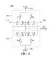
- Fig. 4 is a circuit diagram of a tunable capacitance unit according to an embodiment of the invention.
- the tunable capacitance unit 300 comprises a tuning input 301 and first and second tuning capacitance units 330 and 340.
- the first tuning capacitance comprises a first pair of accumulation-mode MOS varactors CV1/CV2, a first pair of blocking capacitors C1/C2, and a first pair of biasing resistors R1/R2.
- the second tuning capacitance comprises a second pair of accumulation-mode MOS varactors CV3/CV4, a second pair of blocking capacitors C3/C4, and a second pair of biasing resistors R3/R4.
- FIG. 5A A symbol, a schematic and a cross section of the accumulation-mode MOS varactors CV1/CV2 and CV3/CV4 in Fig. 4 are respectively shown in Fig. 5A, Fig 5B, and Fig. 5C .
- each of the accumulation-mode MOS varactors CV1/CV2 and CV3/CV4 has a N-well 401, source/drain regions 403, a gate dielectric (not shown in the figure), and a gate 405 over the gate dielectric.
- the tuning input 301 receives a tuning voltage Vtune.
- the first pair of accumulation-mode MOS varactors CV1/CV2 is coupled between the tuning input 301 and the first pair of blocking capacitors C1/C2 and biasing resistors R1/R2. More specifically, source/drains of the first pair of accumulation-mode MOS varactors CV1/CV2 are coupled to the tuning input 301.
- the first pair of blocking capacitors C1/C2 is coupled to a respective gate of the first pair of the accumulation-mode MOS varactors CV1/CV2 and to a respective one of the circuit nodes 310/320.
- the first pair of biasing resistors R1/R2 is coupled to a respective gate of the first pair of the accumulation-mode MOS varactors CV1/CV2 and to a first bias terminal 303 receiving a first reference voltage Vref1.
- the second pair of accumulation-mode MOS varactors CV3/CV4 is coupled between the tuning input 301 and the second pair of blocking capacitors C3/C4 and biasing resistors R3/R4. More specifically, source/drains of the second pair of accumulation-mode MOS varactors CV3/CV4 are coupled to the tuning input 301.
- the second pair of blocking capacitors C3/C4 is coupled to a respective gate of the second pair of the accumulation-mode MOS varactors CV3/CV4 and to a respective one of the circuit nodes 310/320.
- the second pair of biasing resistors R1/R2 is coupled to a respective gate of the second pair of the accumulation-mode MOS varactors CV3/CV4 and to a second bias terminal 305 receiving a second reference voltage Vref2.
- the first reference voltage Vref1 and the second reference voltage Vref2 are symmetrical to a predetermined voltage Vnom.
- the first and second reference voltages Vref1 and Vref2 can be expressed as Vnom+ ⁇ V and Vnom- ⁇ V.
- the tunable capacitance unit TCU in Fig. 1A, 1B or 1C can be replaced by that in Fig. 3 .
- the first and second reference voltages can be biased such that different K VCO is obtained.
- An exemplary bias table is shown in Table I.
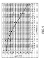
- Fig. 6 is a diagram showing an equivalent capacitance versus a tuning voltage Vtune of the tunable capacitance unit in Fig. 4 .
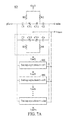
- Fig. 7A is a circuit diagram showing an expansive variant of the tunable capacitance unit in Fig. 4 .
- the tunable capacitance unit further comprises a third tuning capacitance unit 630 and a fourth tuning capacitance unit 640. As with the tuning capacitance units in Fig.
- the third tuning capacitance unit 630 comprises a third pair of accumulation-mode MOS varactors with source/drains thereof coupled to the tuning input, a third pair of blocking capacitors coupled to a respective gate of the third pair of accumulation-mode MOS varactors and to a respective one of the circuit nodes, a third pair of biasing resistors coupled to a respective gate of the third pair of accumulation-mode MOS varactors and to a third bias terminal receiving a third reference voltage.
- the fourth tuning capacitance unit 640 comprises a fourth pair of accumulation-mode MOS varactors with source/drains thereof coupled to the tuning input, a fourth pair of blocking capacitors coupled to a respective gate of the third pair of accumulation-mode MOS varactors and to a respective one of the circuit nodes, and a fourth pair of biasing resistors coupled to a respective gate of the fourth pair of accumulation-mode MOS varactors and to a fourth bias terminal receiving a fourth reference voltage, wherein the third and fourth reference voltages are symmetrical to the predetermined voltage.
- the tunable capacitance unit can comprise more tuning capacitance units.
- Vcenter Vrefn + Vref ⁇ m + n + 1 2 , wherein Vcenter is a tuning voltage at which the tunable capacitance unit has a linear change in C TCU with respect to the tuning voltage Vtune, as shown in Fig. 7B .
- Fig 8 is circuit diagram showing an expansive variant of the tunable capacitance unit in Fig. 4 .
- the tunable capacitance unit 700 in Fig. 8 comprises the disclosed components as shown in Fig. 4 .
- the tunable capacitance unit 700 further comprises a voltage divider 710 and first and second multiplexors 720 and 730.
- the voltage divider 710 comprises a plurality of resistors R connected in series between a pair of fixed voltages and provides a plurality of reference voltages V1, V2, ..., Vm-1, and Vm.
- Each of the first and second multiplexors 720 and 730 is coupled between a respective one of the bias terminals 303 (or 305) and the voltage divider 710.
- the predetermined voltage Vnom is here a center voltage Vcenter of the voltage divider 710 and the first and second reference voltages Vref1 and Vref2 are selected from the reference voltages V1, V2, ..., Vm-1, and Vm.
- the tunable capacitance unit 700 further comprises a temperature compensation circuit 740.
- the temperature compensation circuit provides at least one of the fixed voltages such that characteristic variation of the tunable capacitance unit due to temperature variation is compensated.
- Fig. 9 is a diagram showing simulation results of K TCU versus ⁇ V of the tunable capacitance unit in Fig. 3 .
- square data points are data points of a process corner with fast NMOS and PMOS devices
- diamond data points represent those of a process corner with typical NMOS and PMOS devices
- triangle data points represent those of a process corner with slow NMOS and PMOS devices.
- center operating frequency of the LC VCO does not vary with a different bias reference voltage significantly, which is also desirable to circuit designers. Since different process corners does not result in significant change in K TCU , characteristics of the LC VCO are not significantly influenced by process variation.
- Fig. 10 is a diagram showing simulation results of K TCU versus a tuning voltage Vtune of the tunable capacitance unit in Fig. 3 under different ⁇ V values.
- K TCU does not change significantly with the tuning voltage Vtune within a ⁇ V range, which is desirable to circuit designers.
- K TCU remains nearly constant within a small tuning voltage range.
- the a circuit designer desires a constant K TCU over a wide tuning voltage range, only a small tunable K TCU range is obtained.
- Fig. 11 is a diagram showing simulation results of an equivalent capacitance versus ⁇ V of the tunable capacitance unit in Fig. 4 for different process corners when the tuning voltage Vtune is 0.7V.
- square data points are data points of a process corner with fast NMOS and PMOS devices
- diamond data points represent those of a process corner with typical NMOS and PMOS devices
- triangle data points represent those of a process corner with slow NMOS and PMOS devices.
- the equivalent capacitance of the tunable capacitance unit remains nearly constant over a very wide ⁇ V range.
- different process corners do not result in a significant change in the equivalent capacitance of the tunable capacitance unit.
- characteristics of the LC VCO are not significantly influenced by process variation.
- Fig. 12A is a diagram showing simulation results of K TCU versus a tuning voltage Vtune of the tunable capacitance unit in Fig. 4 at different temperatures (-20°C and 85°C). It is shown that temperature variation results in significant change in K TCU , which is not desirable to circuit designers. To overcome such temperature effect, a temperature compensation mechanism is added to the tunable capacitance unit.
- Fig. 12B is another diagram showing simulation results of K TCU versus a tuning voltage Vtune of the tunable capacitance unit at different temperatures (-20°C, room temperature, and 85°C). Since temperature variation results in significant change in K TCU , a temperature compensation mechanism is desirable such that characteristics of the LC VCO does not change significantly with temperature variation.
- a center voltage thereof is temperature compensated via temperature compensation of at least one of the fixed voltages.
- temperature variation may not result in significant change in K TCU .
- temperature effect of the tunable capacitance unit is compensated.
- a LC voltage controlled oscillator (VCO) with a tunable capacitance unit is disclosed.
- the disclosed LC VCO has a constant gain (K VCO ) within a wide frequency band and a bandwidth of a phase locked loop (PLL) circuit can be tuned by tuning a gain Kvco of the LC VCO.
- K VCO constant gain
- PLL phase locked loop
Landscapes
- Engineering & Computer Science (AREA)
- Power Engineering (AREA)
- Inductance-Capacitance Distribution Constants And Capacitance-Resistance Oscillators (AREA)
Abstract
Description
- The invention relates to a voltage controlled oscillator (VCO) and, in particular, to an LC VCO with a tunable capacitance unit.
-
Figs 1A, 1B and 1C are respectively a circuit diagram of a LC tank voltage controlled oscillator (VCO) 100, or an LC VCO. The LC VCO 100 typically comprises anLC tank circuit 110 and anegative resistance circuit 120. TheLC tank circuit 110 comprises an inductor L and a tunable capacitance unit TCU. A capacitance of the tunable capacitance unit TCU is typically tuned by a tuning voltage Vtune. Thenegative resistance circuit 120 comprises a pair of MOS transistors, each having a gate, a source and a drain. The gates of the MOS transistors are cross-coupled to the drains thereof and sources thereof are coupled to a fixed voltage, Vcc or ground. In addition, theLC tank circuit 110 further comprises a switch capacitor array SCA such that the LCVCO 100 becomes a wide band LC VCO with a wide operating frequency range. The tunable capacitance unit TCU is typically used to tune an oscillating frequency of theLC VCO 100 if the switch capacitor array SCA is fixed to a single sub-band. When the tuning voltage Vtune goes high or low, the capacitance of the tunable capacitance unit TCU changes and results in frequency change of theLC VCO 100. -
Fig. 2 shows a typical characteristic of a gain of the LC VCO shown inFig. 1A, 1B or 1C versus a tuning voltage thereof within different sub-bands. A gain Kvco of the LC VCO is defined as a change in an oscillating frequency thereof divided by a change in a tuning voltage thereof, i.e.

Fig. 2 are not linear and not desirable to circuit designers. -
Fig. 3 is a circuit diagram of a conventional tunable capacitive component as disclosed inUS patent 6,995,626 . The tunable capacitive component comprises a pair of MOS transistors Ma1/Mb1 (Ma2/Mb2,..., MaN/MbN) gate connections of which are connected via arespective coupling capacitance 10 to a pair ofcircuit nodes 6/7 between which the tuned capacitance can be tapped off. The four load connections of the MOS transistors Ma1/Mb1 (Ma2/Mb2,..., MaN/MbN) are connected to one another. Atuning input 5 is coupled to the transistor pair Ma1/Mb1 (Ma2/Mb2,..., MaN/MbN) such that a tuning voltage is provided thereto. In addition, the gate connections of the pair of MOS transistors Ma1/Mb1 (Ma2/Mb2,..., MaN/MbN) are coupled to a reference signal input Vref1 (Vref12,..., Vref1N) via resistors R1 (R 2,..., R N). In this arrangement, the reference signal input is designed to set the operating point of the transistors. The tunable capacitance has a wide tuning range and also a low series resistance and permits good linearity properties on account of the operating point setting. However, such arrangement cannot provide a tunable Kvco according to an oscillating frequency of an LC oscillator. - An embodiment of tunable capacitance unit coupled between a pair of circuit nodes comprises a tuning input supplying a tuning voltage, and first and second tuning capacitance units. Each of the tuning capacitance units comprises a pair of accumulation-mode MOS varactors with source/drains thereof coupled to the tuning input, a pair of blocking capacitors coupled to a respective gate of the accumulation-mode MOS varactors and to a respective one of the circuit nodes, and a pair of biasing resistors coupled to a respective gate of the accumulation-mode MOS varactors and to a respective bias terminal receiving a respective reference voltage. The reference voltages received by the first and second tuning capacitance units are symmetrical to a predetermined voltage.
- An embodiment of a LC voltage controlled oscillator comprises a LC tank circuit and a negative resistance circuit coupled to the LC tank circuit. The LC tank circuit comprises an inductor and the disclosed tunable capacitance unit.
- A LC voltage controlled oscillator (VCO) with a tunable capacitance unit is disclosed. The disclosed LC VCO has a constant gain (KVCO) within a wide frequency band and a bandwidth of a phase locked loop (PLL) circuit can be tuned by tuning a gain Kvco of the LC VCO. In addition, requirements for a compensation current of a charge pump circuit in the PLL circuit are relaxed and degradation of out-of-band phase noise due to high KVCO can also be avoided.
- A detailed description is given in the following embodiments with reference to the accompanying drawings.
- The invention can be more fully understood by reading the subsequent detailed description and examples with references made to the accompanying drawings, wherein:
-
Figs 1A, 1B and 1C are respectively a circuit diagram of a LC tank voltage controlled oscillator (VCO) 100, or an LC VCO; -
Fig. 2 shows a typical characteristic of a gain of the LC VCO shown inFig. 1A, 1B or 1C versus a tuning voltage thereof within different sub-bands; -
Fig. 3 is a circuit diagram of a conventional tunable capacitive component disclosed inUS patent 6,995,626 ; -
Fig. 4 is a circuit diagram of a tunable capacitance unit according to an embodiment of the invention; -
Figs. 5A, 5B, and 5C are respectively schematic diagrams of a symbol, a schematic, and a cross section of the tunable capacitance unit inFig. 4 ; -
Fig. 6 is a diagram showing an equivalent capacitance versus a tuning voltage Vtune of the tunable capacitance unit inFig. 4 ; -
Fig. 7A is a circuit diagram showing an expansive variant of the tunable capacitance unit inFig. 4 ; -
Fig. 7B is a diagram showing an equivalent capacitance versus a tuning voltage of the tunable capacitance unit inFig. 7A ; -
Fig 8 is a circuit diagram showing an expansive variant of the tunable capacitance unit under process corner conditions inFig. 4 ; -
Fig. 9 is a diagram showing simulated results of KTCU versus ΔV of the tunable capacitance unit inFig. 4 ; -
Fig. 10 is a diagram showing simulated results of KTCU versus a tuning voltage of the tunable capacitance unit inFig. 4 under different ΔV values; and -
Fig. 11 is a diagram showing simulated results of an equivalent capacitance versus ΔV of the tunable capacitance unit inFig. 4 for different process corners when the tuning voltage Vtune is 0.7V; -
Fig. 12A is a diagram showing simulated results of KTCU versus a tuning voltage Vtune of the tunable capacitance unit inFig. 4 at different temperatures (-20°C and 85°C); and -
Fig. 12B is a diagram showing simulated results of KTCU versus a tuning voltage Vtune of the tunable capacitance unit at different temperatures (-20°C, room temperature, and 85°C). - The following description is of the best-contemplated mode of carrying out the invention. This description is made for the purpose of illustrating the general principles of the invention and should not be taken in a limiting sense. The scope of the invention is best determined by reference to the appended claims.
-
Fig. 4 is a circuit diagram of a tunable capacitance unit according to an embodiment of the invention. Thetunable capacitance unit 300 comprises atuning input 301 and first and secondtuning capacitance units Fig. 4 are respectively shown inFig. 5A, Fig 5B, and Fig. 5C . As shown inFig. 5C , each of the accumulation-mode MOS varactors CV1/CV2 and CV3/CV4 has a N-well 401, source/drain regions 403, a gate dielectric (not shown in the figure), and agate 405 over the gate dielectric. InFig. 4 , the tuninginput 301 receives a tuning voltage Vtune. The first pair of accumulation-mode MOS varactors CV1/CV2 is coupled between the tuninginput 301 and the first pair of blocking capacitors C1/C2 and biasing resistors R1/R2. More specifically, source/drains of the first pair of accumulation-mode MOS varactors CV1/CV2 are coupled to the tuninginput 301. The first pair of blocking capacitors C1/C2 is coupled to a respective gate of the first pair of the accumulation-mode MOS varactors CV1/CV2 and to a respective one of thecircuit nodes 310/320. The first pair of biasing resistors R1/R2 is coupled to a respective gate of the first pair of the accumulation-mode MOS varactors CV1/CV2 and to a first bias terminal 303 receiving a first reference voltage Vref1. Similarly, the second pair of accumulation-mode MOS varactors CV3/CV4 is coupled between the tuninginput 301 and the second pair of blocking capacitors C3/C4 and biasing resistors R3/R4. More specifically, source/drains of the second pair of accumulation-mode MOS varactors CV3/CV4 are coupled to the tuninginput 301. The second pair of blocking capacitors C3/C4 is coupled to a respective gate of the second pair of the accumulation-mode MOS varactors CV3/CV4 and to a respective one of thecircuit nodes 310/320. The second pair of biasing resistors R1/R2 is coupled to a respective gate of the second pair of the accumulation-mode MOS varactors CV3/CV4 and to asecond bias terminal 305 receiving a second reference voltage Vref2. The first reference voltage Vref1 and the second reference voltage Vref2 are symmetrical to a predetermined voltage Vnom. In other words, the first and second reference voltages Vref1 and Vref2 can be expressed as Vnom+ΔV and Vnom-ΔV. - The tunable capacitance unit TCU in
Fig. 1A, 1B or 1C can be replaced by that inFig. 3 . Thus, the first and second reference voltages can be biased such that different KVCO is obtained. An exemplary bias table is shown in Table I.Fig. 6 is a diagram showing an equivalent capacitance versus a tuning voltage Vtune of the tunable capacitance unit inFig. 4 . When the first and second reference voltages are biased atbias condition 
Table I Bias condition Vref1(V) Vref2(V) K TCU1 Vnom Vnom m1 2 Vnom+ΔV1 Vnom- ΔV1 m2 3 Vnom+ΔV2 Vnom-ΔV2 m3 -
Fig. 7A is a circuit diagram showing an expansive variant of the tunable capacitance unit inFig. 4 . In addition to the first and second tuning capacitance units, the tunable capacitance unit further comprises a thirdtuning capacitance unit 630 and a fourthtuning capacitance unit 640. As with the tuning capacitance units inFig. 4 , the thirdtuning capacitance unit 630 comprises a third pair of accumulation-mode MOS varactors with source/drains thereof coupled to the tuning input, a third pair of blocking capacitors coupled to a respective gate of the third pair of accumulation-mode MOS varactors and to a respective one of the circuit nodes, a third pair of biasing resistors coupled to a respective gate of the third pair of accumulation-mode MOS varactors and to a third bias terminal receiving a third reference voltage. The fourthtuning capacitance unit 640 comprises a fourth pair of accumulation-mode MOS varactors with source/drains thereof coupled to the tuning input, a fourth pair of blocking capacitors coupled to a respective gate of the third pair of accumulation-mode MOS varactors and to a respective one of the circuit nodes, and a fourth pair of biasing resistors coupled to a respective gate of the fourth pair of accumulation-mode MOS varactors and to a fourth bias terminal receiving a fourth reference voltage, wherein the third and fourth reference voltages are symmetrical to the predetermined voltage. In addition, the tunable capacitance unit can comprise more tuning capacitance units. To keep the equivalent capacitance CTCU of the tunable capacitance unit fixed when tuning KTCU thereof, the reference voltages received by the tunable capacitance unit have the following relationship:
Fig. 7B . -
Fig 8 is circuit diagram showing an expansive variant of the tunable capacitance unit inFig. 4 . The tunable capacitance unit 700 inFig. 8 comprises the disclosed components as shown inFig. 4 . In addition, the tunable capacitance unit 700 further comprises avoltage divider 710 and first andsecond multiplexors voltage divider 710 comprises a plurality of resistors R connected in series between a pair of fixed voltages and provides a plurality of reference voltages V1, V2, ..., Vm-1, and Vm. Each of the first andsecond multiplexors voltage divider 710. The predetermined voltage Vnom is here a center voltage Vcenter of thevoltage divider 710 and the first and second reference voltages Vref1 and Vref2 are selected from the reference voltages V1, V2, ..., Vm-1, and Vm. In addition, the tunable capacitance unit 700 further comprises atemperature compensation circuit 740. The temperature compensation circuit provides at least one of the fixed voltages such that characteristic variation of the tunable capacitance unit due to temperature variation is compensated. -
Fig. 9 is a diagram showing simulation results of KTCU versus ΔV of the tunable capacitance unit inFig. 3 . InFig. 9 , square data points are data points of a process corner with fast NMOS and PMOS devices, diamond data points represent those of a process corner with typical NMOS and PMOS devices, and triangle data points represent those of a process corner with slow NMOS and PMOS devices. It is found that KTCU has a linear change with respect to ΔV from ΔV=0.26V to ΔV=0.47V and is thus more easily controlled. In addition, in such a linear region, center operating frequency of the LC VCO does not vary with a different bias reference voltage significantly, which is also desirable to circuit designers. Since different process corners does not result in significant change in KTCU, characteristics of the LC VCO are not significantly influenced by process variation. -
Fig. 10 is a diagram showing simulation results of KTCU versus a tuning voltage Vtune of the tunable capacitance unit inFig. 3 under different ΔV values.Fig. 10 also shows that KTCU has a linear change with respect to ΔV from ΔV=0.265V to ΔV=0.465V and is thus more easily controlled. In addition, it is found that KTCU does not change significantly with the tuning voltage Vtune within a ΔV range, which is desirable to circuit designers. As a result, if a wider tunable KTCU range is desired, then KTCU remains nearly constant within a small tuning voltage range. To the contrary, if the a circuit designer desires a constant KTCU over a wide tuning voltage range, only a small tunable KTCU range is obtained. -
Fig. 11 is a diagram showing simulation results of an equivalent capacitance versus ΔV of the tunable capacitance unit inFig. 4 for different process corners when the tuning voltage Vtune is 0.7V. InFig. 11 , square data points are data points of a process corner with fast NMOS and PMOS devices, diamond data points represent those of a process corner with typical NMOS and PMOS devices, and triangle data points represent those of a process corner with slow NMOS and PMOS devices. The equivalent capacitance of the tunable capacitance unit remains nearly constant over a very wide ΔV range. In addition, different process corners do not result in a significant change in the equivalent capacitance of the tunable capacitance unit. As a result, characteristics of the LC VCO are not significantly influenced by process variation. -
Fig. 12A is a diagram showing simulation results of KTCU versus a tuning voltage Vtune of the tunable capacitance unit inFig. 4 at different temperatures (-20°C and 85°C). It is shown that temperature variation results in significant change in KTCU, which is not desirable to circuit designers. To overcome such temperature effect, a temperature compensation mechanism is added to the tunable capacitance unit.Fig. 12B is another diagram showing simulation results of KTCU versus a tuning voltage Vtune of the tunable capacitance unit at different temperatures (-20°C, room temperature, and 85°C). Since temperature variation results in significant change in KTCU, a temperature compensation mechanism is desirable such that characteristics of the LC VCO does not change significantly with temperature variation. If there is atemperature compensation circuit 740 in the tunable capacitance unit as shown inFig. 8 , a center voltage thereof is temperature compensated via temperature compensation of at least one of the fixed voltages. For example, Vref1=0.49V+ΔV and Vref2=0.49V-ΔV for high temperature condition, and Vref1=0.54V+ΔV and Vref2=0.54V-ΔV for low temperature condition. As a result, temperature variation may not result in significant change in KTCU. In other words, temperature effect of the tunable capacitance unit is compensated. - A LC voltage controlled oscillator (VCO) with a tunable capacitance unit is disclosed. The disclosed LC VCO has a constant gain (KVCO) within a wide frequency band and a bandwidth of a phase locked loop (PLL) circuit can be tuned by tuning a gain Kvco of the LC VCO. In addition, requirements for a compensation current of a charge pump circuit in the PLL circuit are relaxed and degradation of out-of-band phase noise due to high Kvco can also be avoided.
- While the invention has been described by way of example and in terms of preferred embodiment, it is to be understood that the invention is not limited thereto. To the contrary, it is intended to cover various modifications and similar arrangements as would be apparent to those skilled in the art. Therefore, the scope of the appended claims should be accorded the broadest interpretation so as to encompass all such modifications and similar arrangements.
Claims (11)
- A tunable capacitance unit (300) coupled between a pair of circuit nodes, comprising:a tuning input (301) for receiving a tuning voltage (Vtune);a first pair of accumulation-mode MOS varactors (CV1, CV2) with source/drains thereof coupled to the tuning input (301);a first pair of blocking capacitors (C1, C2) coupled to a respective gate of the first pair of accumulation-mode MOS varactors (CV1, CV2) and to a respective one of the circuit nodes;a first pair of biasing resistors (R1, R2) coupled to a respective gate of the first pair of accumulation-mode MOS varactors (CV1, CV2) and to a first bias terminal receiving a first reference voltage (Vref1);a second pair of accumulation-mode MOS varactors (CV3, CV4) with source/drains thereof coupled to the tuning input (301);a second pair of blocking capacitors (C3, C4) coupled to a respective gate of the second pair of accumulation-mode MOS varactors (CV3, CV4) and to a respective one of the circuit nodes; anda second pair of biasing resistors (R3, R4) coupled to a respective gate of the second pair of accumulation-mode MOS varactors (CV3, CV4) and to a second bias terminal receiving a second reference voltage (Vref2);wherein the first and second reference voltages (Vref1, Vref2) are symmetrical to a predetermined voltage (Vnom).
- The tunable capacitance unit (300) as claimed in claim 1, further comprising a voltage divider (710) comprising a plurality of resistors connected in series between a pair of fixed voltages and providing a plurality of reference voltages and first and second multiplexors (720, 730) each coupled between a respective one of the bias terminals and the voltage divider, wherein the predetermined voltage is a center voltage (Vcenter) of the voltage divider (710) and the first and second reference voltages (Vref1, Vref2) are selected from the reference voltages.
- The tunable capacitance unit (300) as claimed in claim 2, further comprising a temperature compensation circuit (740) coupled to voltage divider (710) and providing at least one of the fixed voltages.
- The tunable capacitance unit (300) as claimed in claim 1, further comprising a third pair of accumulation-mode MOS varactors with source/drains thereof coupled to the tuning input, a third pair of blocking capacitors coupled to a respective gate of the third pair of accumulation-mode MOS varactors and to a respective one of the circuit nodes, a third pair of biasing resistors coupled to a respective gate of the third pair of accumulation-mode MOS varactors and to a third bias terminal receiving a third reference voltage (630), a fourth pair of accumulation-mode MOS varactors with source/drains thereof coupled to the tuning input, a fourth pair of blocking capacitors coupled to a respective gate of the third pair of accumulation-mode MOS varactors and to a respective one of the circuit nodes, and a fourth pair of biasing resistors coupled to a respective gate of the fourth pair of accumulation-mode MOS varactors and to a fourth bias terminal receiving a fourth reference voltage (640), wherein the third and fourth reference voltages are symmetrical to the predetermined voltage.
- A LC voltage controlled oscillator (100), comprising:an LC tank circuit (110) comprising an inductor (L) and a tunable capacitance unit (300); anda negative resistance circuit (120) coupled to the LC tank circuit (110);wherein the tunable capacitance unit (300) comprises:a tuning input (301) for receiving a tuning voltage (Vtune);a first pair of accumulation-mode MOS varactors (CV1, CV2) with source/drains thereof coupled to the tuning input (301);a first pair of blocking capacitors (C1, C2) coupled to a respective gate of the first pair of accumulation-mode MOS varactors (CV1, CV2) and to a respective one of the circuit nodes;a first pair of biasing resistors (R1, R2) coupled to a respective gate of the first pair of accumulation-mode MOS varactors (CV1, CV2) and to a first bias terminal receiving a first reference voltage (Vref1);a second pair of accumulation-mode MOS varactors (CV3, CV4) with source/drains thereof coupled to the tuning input (301);a second pair of blocking capacitors (C3, C4) coupled to a respective gate of the second pair of accumulation-mode MOS varactors (CV3, CV4) and to a respective one of the circuit nodes; anda second pair of biasing resistors (R3, R4) coupled to a respective gate of the second pair of accumulation-mode MOS varactors (Cv3, CV4) and to a second bias terminal receiving a second reference voltage (Vref2);wherein the first and second reference voltages (Vref1, Vref2) are symmetrical to a predetermined voltage (Vnom).
- The LC voltage controlled oscillator (100) as claimed in claim 5, wherein the negative resistance circuit (120) comprises a pair of transistors having first, second and third terminals, wherein the first terminals are cross-coupled to the second terminals thereof and the third terminals are coupled to a fixed voltage.
- The LC voltage controlled oscillator (100) as claimed in claim 5, wherein the tunable capacitance unit (300) further comprises a voltage divider (710) comprising a plurality of resistors connected in series between a pair of fixed voltages and providing a plurality of reference voltages and first and second multiplexors (720, 730) each coupled between a respective one of the bias terminals and the voltage divider (710), wherein the predetermined voltage is a center voltage (Vcenter) of the voltage divider (710) and the first and second reference voltages (Vref1, Vref2) are selected from the reference voltages.
- The LC voltage controlled oscillator (100) as claimed in claim 7, wherein the multiplexors (720, 730) are controlled according to an output frequency of the LC voltage controlled oscillator (100).
- The LC voltage controlled oscillator (100) as claimed in claim 7, wherein the tunable capacitance unit (300) further comprises a temperature compensation circuit (740) coupled to voltage divider (710) and providing at least one of the fixed voltages.
- The LC voltage controlled oscillator (100) as claimed in claim 5, wherein the tunable capacitance unit (300) further comprises a third pair of accumulation-mode MOS varactors with source/drains thereof coupled to the tuning input, a third pair of blocking capacitors coupled to a respective gate of the third pair of
accumulation-mode MOS varactors and to a respective one of the circuit nodes, a third pair of biasing resistors coupled to a respective gate of the third pair of accumulation-mode MOS varactors and to a third bias terminal receiving a third reference voltage (630), a fourth pair of accumulation-mode MOS varactors with source/drains thereof coupled to the tuning input, a fourth pair of blocking capacitors coupled to a respective gate of the third pair of accumulation-mode MOS varactors and to a respective one of the circuit nodes, and a fourth pair of biasing resistors coupled to a respective gate of the fourth pair of accumulation-mode MOS varactors and to a fourth bias terminal receiving a fourth reference voltage (640), wherein the third and fourth reference voltages (Vref1, Vref2) are symmetrical to the predetermined voltage (Vnom). - The LC voltage controlled oscillator (100) as claimed in claim 5, wherein the LC tank circuit (110) further comprises a switch capacitor array (SCA) coupled to the inductor (L) and the tunable capacitance unit (300).
Applications Claiming Priority (1)
| Application Number | Priority Date | Filing Date | Title |
|---|---|---|---|
| US11/800,403 US20080272851A1 (en) | 2007-05-04 | 2007-05-04 | LC voltage controlled oscillator with tunable capacitance unit |
Publications (1)
| Publication Number | Publication Date |
|---|---|
| EP1988628A1 true EP1988628A1 (en) | 2008-11-05 |
Family
ID=38671283
Family Applications (1)
| Application Number | Title | Priority Date | Filing Date |
|---|---|---|---|
| EP07115764A Withdrawn EP1988628A1 (en) | 2007-05-04 | 2007-09-05 | LC voltage controlled oscillator with tunable capacitance unit |
Country Status (4)
| Country | Link |
|---|---|
| US (1) | US20080272851A1 (en) |
| EP (1) | EP1988628A1 (en) |
| CN (1) | CN101299592A (en) |
| TW (1) | TW200845580A (en) |
Cited By (5)
| Publication number | Priority date | Publication date | Assignee | Title |
|---|---|---|---|---|
| WO2011129951A1 (en) * | 2010-04-13 | 2011-10-20 | Xilinx, Inc. | Varactor circuit and voltage-controlled oscillation |
| WO2012048036A3 (en) * | 2010-10-05 | 2012-08-02 | Qualcomm Incorporated | Reconfigurable local oscillator for optimal noise performance in a multi-standard transceiver |
| WO2013137867A1 (en) * | 2012-03-13 | 2013-09-19 | Intel Corporation | Temperature compensation for oscillator |
| CN104300967A (en) * | 2014-09-19 | 2015-01-21 | 杭州迦美信芯通讯技术有限公司 | Voltage-controlled oscillator circuit with frequency not changing with temperature |
| EP3813252A1 (en) * | 2019-10-24 | 2021-04-28 | Nxp B.V. | Variable reactance apparatus for dynamic gain switching of tunable oscillator |
Families Citing this family (26)
| Publication number | Priority date | Publication date | Assignee | Title |
|---|---|---|---|---|
| US20100102859A1 (en) * | 2008-10-29 | 2010-04-29 | Texas Instruments Incorporated | Lc voltage controlled oscillator tank with linearized frequency control |
| US8031019B2 (en) * | 2009-02-02 | 2011-10-04 | Qualcomm Incorporated | Integrated voltage-controlled oscillator circuits |
| US8736392B2 (en) * | 2009-03-18 | 2014-05-27 | Qualcomm Incorporated | Transformer-based CMOS oscillators |
| US8058938B2 (en) * | 2009-04-30 | 2011-11-15 | Project Ft, Inc. | Voltage controlled oscillator |
| CN101944880B (en) * | 2009-07-08 | 2013-09-25 | 杭州中科微电子有限公司 | VCO tuning curve compensation method and module thereof |
| CN102201785B (en) * | 2010-03-23 | 2013-06-26 | 北京大学 | Ultra-low power consumption voltage-controlled oscillator circuit and signal processing method thereof |
| US8493114B2 (en) * | 2011-07-06 | 2013-07-23 | Mediatek Inc. | Temperature compensation circuit and synthesizer using the temperature compensation circuit |
| CN103891046B (en) * | 2011-10-26 | 2016-05-04 | 株式会社村田制作所 | communication circuit |
| TWI585660B (en) * | 2012-01-06 | 2017-06-01 | 新唐科技股份有限公司 | Touch sensing apparatus |
| CN103197812B (en) | 2012-01-06 | 2016-06-01 | 新唐科技股份有限公司 | Touch control induction device |
| EP2782249A1 (en) * | 2013-03-19 | 2014-09-24 | Dialog Semiconductor B.V. | Electrically programmable electronic load |
| CN104682873A (en) * | 2013-11-27 | 2015-06-03 | 中国航天科工集团第三研究院第八三五七研究所 | Ultra-wide-octave voltage controlled oscillator (VCO) |
| FR3018016A1 (en) * | 2014-02-26 | 2015-08-28 | St Microelectronics Tours Sas | BST CAPACITOR |
| WO2015196160A1 (en) | 2014-06-19 | 2015-12-23 | Project Ft, Inc. | Memoryless active device which traps even harmonic signals |
| DE102015102600A1 (en) * | 2015-02-24 | 2016-08-25 | Infineon Technologies Ag | Communication device and method for calibrating an oscillator |
| CN104852732B (en) * | 2015-05-28 | 2017-09-05 | 中国科学技术大学先进技术研究院 | A kind of voltage controlled oscillator of low-power consumption low noise high linear gain |
| CN106330097B (en) * | 2016-08-19 | 2019-02-19 | 西安电子科技大学 | InP HBT Voltage Controlled Oscillator Based on Coupled Transmission Line |
| CN106788408A (en) * | 2016-12-06 | 2017-05-31 | 天津北芯微科技有限公司 | A kind of constant LC VCO of wide-voltage range tuning gain |
| CN106603012B (en) * | 2016-12-09 | 2020-06-30 | 重庆西南集成电路设计有限责任公司 | Broadband temperature compensation voltage-controlled oscillator, temperature compensation method and voltage generation circuit |
| JP6656195B2 (en) * | 2017-03-15 | 2020-03-04 | 株式会社東芝 | Voltage controlled oscillator |
| US10715158B1 (en) | 2019-04-10 | 2020-07-14 | Synopsys, Inc. | Phase-locked loop (PLL) with calibration circuit |
| US11342883B1 (en) * | 2021-05-11 | 2022-05-24 | Realtek Semiconductor Corp. | Voltage-controlled oscillator of programmable gain |
| US11569814B1 (en) * | 2021-10-15 | 2023-01-31 | Analog Bits, Inc. | Variable capacitance circuit for phase locked loops |
| CN116633271A (en) * | 2023-05-31 | 2023-08-22 | 成都电科星拓科技有限公司 | Method, circuit, phase-locked loop and chip for solving overvoltage of VCO capacitor switch |
| US12537479B2 (en) | 2024-07-22 | 2026-01-27 | Samsung Electronics Co., Ltd. | Systems for operating a LC-VCO |
| CN119892067B (en) * | 2025-01-09 | 2025-11-25 | 慷智集成电路(上海)有限公司 | Voltage-controlled oscillators, phase-locked loops, electronic equipment and vehicles |
Citations (3)
| Publication number | Priority date | Publication date | Assignee | Title |
|---|---|---|---|---|
| US6292065B1 (en) * | 2000-01-27 | 2001-09-18 | International Business Machines Corporation | Differential control topology for LC VCO |
| EP1505721A1 (en) * | 2003-08-08 | 2005-02-09 | Sony Ericsson Mobile Communications Japan, Inc. | A voltage-controlled oscillator with plural variable MOS capacitance elements |
| EP1598936A1 (en) * | 2004-05-19 | 2005-11-23 | Sony Ericsson Mobile Communications Japan, Inc. | Variable capacitance circuit having on/off switch for variable capacitance function, and voltage controlled oscillator using the variable capacitance circuit |
Family Cites Families (2)
| Publication number | Priority date | Publication date | Assignee | Title |
|---|---|---|---|---|
| DE10209517A1 (en) * | 2002-03-04 | 2003-06-26 | Infineon Technologies Ag | Tunable capacitive component for a liquid crystal oscillator connects circuit nodes via gate connections in metal oxide semiconductor transistors to measure a tuned capacitor |
| CN1972117B (en) * | 2002-10-03 | 2010-08-25 | 松下电器产业株式会社 | Voltage controlled oscillator, wireless communication apparatus |
-
2007
- 2007-05-04 US US11/800,403 patent/US20080272851A1/en not_active Abandoned
- 2007-09-05 EP EP07115764A patent/EP1988628A1/en not_active Withdrawn
-
2008
- 2008-03-04 CN CN200810082383.6A patent/CN101299592A/en active Pending
- 2008-03-07 TW TW097108133A patent/TW200845580A/en unknown
Patent Citations (3)
| Publication number | Priority date | Publication date | Assignee | Title |
|---|---|---|---|---|
| US6292065B1 (en) * | 2000-01-27 | 2001-09-18 | International Business Machines Corporation | Differential control topology for LC VCO |
| EP1505721A1 (en) * | 2003-08-08 | 2005-02-09 | Sony Ericsson Mobile Communications Japan, Inc. | A voltage-controlled oscillator with plural variable MOS capacitance elements |
| EP1598936A1 (en) * | 2004-05-19 | 2005-11-23 | Sony Ericsson Mobile Communications Japan, Inc. | Variable capacitance circuit having on/off switch for variable capacitance function, and voltage controlled oscillator using the variable capacitance circuit |
Non-Patent Citations (1)
| Title |
|---|
| MIRA J ET AL: "Distributed MOS varactor biasing for VCO gain equalization in 0.13/spl mu/m CMOS technology", 6 June 2004, RADIO FREQUENCY INTEGRATED CIRCUITS (RFIC) SYMPOSIUM, 2004. DIGEST OF PAPERS. 2004 IEEE FORT WORTH, TX, USA JUNE 6-8, 2004, PISCATAWAY, NJ, USA,IEEE, PAGE(S) 131-134, ISBN: 0-7803-8333-8, XP010713749 * |
Cited By (9)
| Publication number | Priority date | Publication date | Assignee | Title |
|---|---|---|---|---|
| WO2011129951A1 (en) * | 2010-04-13 | 2011-10-20 | Xilinx, Inc. | Varactor circuit and voltage-controlled oscillation |
| US8134418B2 (en) | 2010-04-13 | 2012-03-13 | Xilinx, Inc. | Varactor circuit and voltage-controlled oscillation |
| WO2012048036A3 (en) * | 2010-10-05 | 2012-08-02 | Qualcomm Incorporated | Reconfigurable local oscillator for optimal noise performance in a multi-standard transceiver |
| US9344100B2 (en) | 2010-10-05 | 2016-05-17 | Qualcomm Incorporated | Reconfigurable local oscillator for optimal noise performance in a multi-standard transceiver |
| WO2013137867A1 (en) * | 2012-03-13 | 2013-09-19 | Intel Corporation | Temperature compensation for oscillator |
| US9231519B2 (en) | 2012-03-13 | 2016-01-05 | Intel Corporation | Temperature compensation for oscillator |
| CN104300967A (en) * | 2014-09-19 | 2015-01-21 | 杭州迦美信芯通讯技术有限公司 | Voltage-controlled oscillator circuit with frequency not changing with temperature |
| EP3813252A1 (en) * | 2019-10-24 | 2021-04-28 | Nxp B.V. | Variable reactance apparatus for dynamic gain switching of tunable oscillator |
| US11114978B2 (en) | 2019-10-24 | 2021-09-07 | Nxp B.V. | Variable reactance apparatus for dynamic gain switching of tunable oscillator |
Also Published As
| Publication number | Publication date |
|---|---|
| US20080272851A1 (en) | 2008-11-06 |
| TW200845580A (en) | 2008-11-16 |
| CN101299592A (en) | 2008-11-05 |
Similar Documents
| Publication | Publication Date | Title |
|---|---|---|
| US20080272851A1 (en) | LC voltage controlled oscillator with tunable capacitance unit | |
| KR101575775B1 (en) | Temperature compensation and coarse tune bank switches in a low phase noise vco | |
| US8253506B2 (en) | Wideband temperature compensated resonator and wideband VCO | |
| US8058938B2 (en) | Voltage controlled oscillator | |
| CN113612445B (en) | Temperature compensation LC voltage-controlled oscillator | |
| US8710930B2 (en) | Differential ring oscillator and method for calibrating the differential ring oscillator | |
| US7183867B2 (en) | Voltage controlled variable capacitor | |
| US20090108947A1 (en) | Voltage Controlled Oscillator | |
| US10833685B1 (en) | Linearized wide tuning range oscillator using magnetic balun/transformer | |
| US10305454B2 (en) | High stable oscillator for various operating mode | |
| US8098109B2 (en) | Differential varactor circuit for a voltage controlled oscillator | |
| US6882233B2 (en) | Variable oscillation frequency resonance circuit and voltage controlled oscillator using the same | |
| US20080315964A1 (en) | Voltage controlled oscillator using tunable active inductor | |
| US20080309423A1 (en) | Voltage control oscillator and oscillation control system | |
| Kumar et al. | A CMOS active inductor based digital and analog dual tuned voltage-controlled oscillator | |
| US7283006B2 (en) | Voltage-controlled oscillator | |
| US20080111642A1 (en) | Apparatus and methods for vco linearization | |
| Karimi et al. | A new modified I-MOS varactor for linear range enhancement | |
| US20090072919A1 (en) | Voltage-controlled oscillator with wide oscillation frequency range and linear characteristics | |
| US7385452B2 (en) | Voltage controlled oscillator using capacitive degeneration | |
| US20090167446A1 (en) | Voltage controlled ring oscillator | |
| US7915967B2 (en) | Frequency-tunable oscillator arrangement | |
| US9520829B1 (en) | Apparatus and method of fine capacitance tuning for high resolution digitally controlled oscillator | |
| JP2008193379A (en) | Tuning circuit adjustment method and receiving circuit | |
| US20070241834A1 (en) | Frequency fine- tuning circuit and voltage-controlled oscillator including the same |
Legal Events
| Date | Code | Title | Description |
|---|---|---|---|
| PUAI | Public reference made under article 153(3) epc to a published international application that has entered the european phase |
Free format text: ORIGINAL CODE: 0009012 |
|
| 17P | Request for examination filed |
Effective date: 20080306 |
|
| AK | Designated contracting states |
Kind code of ref document: A1 Designated state(s): AT BE BG CH CY CZ DE DK EE ES FI FR GB GR HU IE IS IT LI LT LU LV MC MT NL PL PT RO SE SI SK TR |
|
| AX | Request for extension of the european patent |
Extension state: AL BA HR MK RS |
|
| 17Q | First examination report despatched |
Effective date: 20081215 |
|
| AKX | Designation fees paid |
Designated state(s): AT BE BG CH CY CZ DE DK EE ES FI FR GB GR HU IE IS IT LI LT LU LV MC MT NL PL PT RO SE SI SK TR |
|
| STAA | Information on the status of an ep patent application or granted ep patent |
Free format text: STATUS: THE APPLICATION IS DEEMED TO BE WITHDRAWN |
|
| 18D | Application deemed to be withdrawn |
Effective date: 20090428 |