EP1988414A1 - Optical waveguide - Google Patents
Optical waveguide Download PDFInfo
- Publication number
- EP1988414A1 EP1988414A1 EP08007631A EP08007631A EP1988414A1 EP 1988414 A1 EP1988414 A1 EP 1988414A1 EP 08007631 A EP08007631 A EP 08007631A EP 08007631 A EP08007631 A EP 08007631A EP 1988414 A1 EP1988414 A1 EP 1988414A1
- Authority
- EP
- European Patent Office
- Prior art keywords
- optical waveguide
- cladding layer
- cores
- metal film
- formation
- Prior art date
- Legal status (The legal status is an assumption and is not a legal conclusion. Google has not performed a legal analysis and makes no representation as to the accuracy of the status listed.)
- Withdrawn
Links
- 230000003287 optical effect Effects 0.000 title claims abstract description 62
- 229910052751 metal Inorganic materials 0.000 claims abstract description 41
- 239000002184 metal Substances 0.000 claims abstract description 41
- 239000000758 substrate Substances 0.000 claims abstract description 30
- 238000005253 cladding Methods 0.000 claims description 60
- 239000010408 film Substances 0.000 description 46
- 230000015572 biosynthetic process Effects 0.000 description 34
- 238000000034 method Methods 0.000 description 34
- 239000000463 material Substances 0.000 description 27
- 239000011347 resin Substances 0.000 description 20
- 229920005989 resin Polymers 0.000 description 20
- 238000010438 heat treatment Methods 0.000 description 14
- 230000005855 radiation Effects 0.000 description 13
- BQCADISMDOOEFD-UHFFFAOYSA-N Silver Chemical compound [Ag] BQCADISMDOOEFD-UHFFFAOYSA-N 0.000 description 12
- 238000004519 manufacturing process Methods 0.000 description 12
- 229910052709 silver Inorganic materials 0.000 description 12
- 239000004332 silver Substances 0.000 description 12
- 239000013039 cover film Substances 0.000 description 9
- 238000004544 sputter deposition Methods 0.000 description 9
- 239000002966 varnish Substances 0.000 description 9
- XAGFODPZIPBFFR-UHFFFAOYSA-N aluminium Chemical compound [Al] XAGFODPZIPBFFR-UHFFFAOYSA-N 0.000 description 7
- 238000011161 development Methods 0.000 description 7
- 238000004528 spin coating Methods 0.000 description 7
- 229910052782 aluminium Inorganic materials 0.000 description 6
- 229920001721 polyimide Polymers 0.000 description 5
- 230000009467 reduction Effects 0.000 description 5
- YEJRWHAVMIAJKC-UHFFFAOYSA-N 4-Butyrolactone Chemical compound O=C1CCCO1 YEJRWHAVMIAJKC-UHFFFAOYSA-N 0.000 description 4
- PXHVJJICTQNCMI-UHFFFAOYSA-N Nickel Chemical compound [Ni] PXHVJJICTQNCMI-UHFFFAOYSA-N 0.000 description 4
- VYPSYNLAJGMNEJ-UHFFFAOYSA-N Silicium dioxide Chemical compound O=[Si]=O VYPSYNLAJGMNEJ-UHFFFAOYSA-N 0.000 description 4
- 238000005229 chemical vapour deposition Methods 0.000 description 4
- 238000007747 plating Methods 0.000 description 4
- 239000009719 polyimide resin Substances 0.000 description 4
- 238000012545 processing Methods 0.000 description 4
- 239000000243 solution Substances 0.000 description 4
- 239000007864 aqueous solution Substances 0.000 description 3
- 238000001035 drying Methods 0.000 description 3
- 239000003822 epoxy resin Substances 0.000 description 3
- QSHDDOUJBYECFT-UHFFFAOYSA-N mercury Chemical compound [Hg] QSHDDOUJBYECFT-UHFFFAOYSA-N 0.000 description 3
- 229920000515 polycarbonate Polymers 0.000 description 3
- 239000004417 polycarbonate Substances 0.000 description 3
- 229920000647 polyepoxide Polymers 0.000 description 3
- VYZAMTAEIAYCRO-UHFFFAOYSA-N Chromium Chemical compound [Cr] VYZAMTAEIAYCRO-UHFFFAOYSA-N 0.000 description 2
- RYGMFSIKBFXOCR-UHFFFAOYSA-N Copper Chemical compound [Cu] RYGMFSIKBFXOCR-UHFFFAOYSA-N 0.000 description 2
- 238000005266 casting Methods 0.000 description 2
- 229910052804 chromium Inorganic materials 0.000 description 2
- 239000011651 chromium Substances 0.000 description 2
- 239000011248 coating agent Substances 0.000 description 2
- 238000000576 coating method Methods 0.000 description 2
- 229910052802 copper Inorganic materials 0.000 description 2
- 239000010949 copper Substances 0.000 description 2
- 238000007598 dipping method Methods 0.000 description 2
- LZCLXQDLBQLTDK-UHFFFAOYSA-N ethyl 2-hydroxypropanoate Chemical compound CCOC(=O)C(C)O LZCLXQDLBQLTDK-UHFFFAOYSA-N 0.000 description 2
- 230000010365 information processing Effects 0.000 description 2
- 238000002347 injection Methods 0.000 description 2
- 239000007924 injection Substances 0.000 description 2
- 239000000203 mixture Substances 0.000 description 2
- 229910052759 nickel Inorganic materials 0.000 description 2
- 239000003960 organic solvent Substances 0.000 description 2
- -1 polyethylene naphthalate Polymers 0.000 description 2
- 229920006290 polyethylene naphthalate film Polymers 0.000 description 2
- 239000000377 silicon dioxide Substances 0.000 description 2
- 239000002904 solvent Substances 0.000 description 2
- NQXNYVAALXGLQT-UHFFFAOYSA-N 2-[4-[9-[4-(2-hydroxyethoxy)phenyl]fluoren-9-yl]phenoxy]ethanol Chemical compound C1=CC(OCCO)=CC=C1C1(C=2C=CC(OCCO)=CC=2)C2=CC=CC=C2C2=CC=CC=C21 NQXNYVAALXGLQT-UHFFFAOYSA-N 0.000 description 1
- 206010073306 Exposure to radiation Diseases 0.000 description 1
- 239000004642 Polyimide Substances 0.000 description 1
- XUIMIQQOPSSXEZ-UHFFFAOYSA-N Silicon Chemical compound [Si] XUIMIQQOPSSXEZ-UHFFFAOYSA-N 0.000 description 1
- 239000002253 acid Substances 0.000 description 1
- 125000002723 alicyclic group Chemical group 0.000 description 1
- 239000000956 alloy Substances 0.000 description 1
- 239000001273 butane Substances 0.000 description 1
- YFNONBGXNFCTMM-UHFFFAOYSA-N butoxybenzene Chemical group CCCCOC1=CC=CC=C1 YFNONBGXNFCTMM-UHFFFAOYSA-N 0.000 description 1
- DXXIFYGOFNDTND-UHFFFAOYSA-N carbonic acid;pentan-3-one Chemical compound OC(O)=O.CCC(=O)CC DXXIFYGOFNDTND-UHFFFAOYSA-N 0.000 description 1
- 239000007822 coupling agent Substances 0.000 description 1
- GYZLOYUZLJXAJU-UHFFFAOYSA-N diglycidyl ether Chemical compound C1OC1COCC1CO1 GYZLOYUZLJXAJU-UHFFFAOYSA-N 0.000 description 1
- LTYMSROWYAPPGB-UHFFFAOYSA-N diphenyl sulfide Chemical compound C=1C=CC=CC=1SC1=CC=CC=C1 LTYMSROWYAPPGB-UHFFFAOYSA-N 0.000 description 1
- 229940116333 ethyl lactate Drugs 0.000 description 1
- 239000011521 glass Substances 0.000 description 1
- 238000007654 immersion Methods 0.000 description 1
- 230000006872 improvement Effects 0.000 description 1
- 239000011344 liquid material Substances 0.000 description 1
- 125000002496 methyl group Chemical group [H]C([H])([H])* 0.000 description 1
- 238000012986 modification Methods 0.000 description 1
- 230000004048 modification Effects 0.000 description 1
- OFBQJSOFQDEBGM-UHFFFAOYSA-N n-pentane Natural products CCCCC OFBQJSOFQDEBGM-UHFFFAOYSA-N 0.000 description 1
- 238000000059 patterning Methods 0.000 description 1
- 229920003207 poly(ethylene-2,6-naphthalate) Polymers 0.000 description 1
- 229920000636 poly(norbornene) polymer Polymers 0.000 description 1
- 229920000058 polyacrylate Polymers 0.000 description 1
- 229920000728 polyester Polymers 0.000 description 1
- 239000011112 polyethylene naphthalate Substances 0.000 description 1
- 230000008569 process Effects 0.000 description 1
- 239000011342 resin composition Substances 0.000 description 1
- 229910052710 silicon Inorganic materials 0.000 description 1
- 239000010703 silicon Substances 0.000 description 1
- 239000007921 spray Substances 0.000 description 1
- 239000000126 substance Substances 0.000 description 1
- 229920003002 synthetic resin Polymers 0.000 description 1
- 239000000057 synthetic resin Substances 0.000 description 1
Images




Classifications
-
- G—PHYSICS
- G02—OPTICS
- G02B—OPTICAL ELEMENTS, SYSTEMS OR APPARATUS
- G02B6/00—Light guides; Structural details of arrangements comprising light guides and other optical elements, e.g. couplings
- G02B6/10—Light guides; Structural details of arrangements comprising light guides and other optical elements, e.g. couplings of the optical waveguide type
- G02B6/12—Light guides; Structural details of arrangements comprising light guides and other optical elements, e.g. couplings of the optical waveguide type of the integrated circuit kind
- G02B6/122—Basic optical elements, e.g. light-guiding paths
- G02B6/1221—Basic optical elements, e.g. light-guiding paths made from organic materials
-
- G—PHYSICS
- G02—OPTICS
- G02B—OPTICAL ELEMENTS, SYSTEMS OR APPARATUS
- G02B6/00—Light guides; Structural details of arrangements comprising light guides and other optical elements, e.g. couplings
- G02B6/10—Light guides; Structural details of arrangements comprising light guides and other optical elements, e.g. couplings of the optical waveguide type
- G02B6/12—Light guides; Structural details of arrangements comprising light guides and other optical elements, e.g. couplings of the optical waveguide type of the integrated circuit kind
-
- G—PHYSICS
- G02—OPTICS
- G02B—OPTICAL ELEMENTS, SYSTEMS OR APPARATUS
- G02B6/00—Light guides; Structural details of arrangements comprising light guides and other optical elements, e.g. couplings
- G02B6/10—Light guides; Structural details of arrangements comprising light guides and other optical elements, e.g. couplings of the optical waveguide type
- G02B6/12—Light guides; Structural details of arrangements comprising light guides and other optical elements, e.g. couplings of the optical waveguide type of the integrated circuit kind
- G02B6/13—Integrated optical circuits characterised by the manufacturing method
- G02B6/138—Integrated optical circuits characterised by the manufacturing method by using polymerisation
Definitions
- the present invention relates to an optical waveguide for widespread use in optical communications, optical information processing, and other general optics.
- An optical waveguide is incorporated in an optical device such as an optical waveguide device, an optical integrated circuit, an optical wiring board and the like, and is widely used in the field of optical communications, optical information processing, and other general optics.
- the optical waveguide includes cores serving as a passageway for light and formed in a predetermined pattern, and an under cladding layer and an over cladding layer formed so as to cover the cores (see, for example, JP-A-2005-165138 ).
- Such an optical waveguide is shown in Fig. 6 .
- an under cladding layer 2, cores 3, and an over cladding layer 4 are formed in the order named on a substrate 1 to form the optical waveguide.
- the refractive index of the above-mentioned cores 3 is made higher than that of the under cladding layer 2 and the over cladding layer 4 so that light passing inside the cores 3 does not exit from the cores 3.
- the cores 3, the under cladding layer 2 and the over cladding layer 4 are in general made of a synthetic resin.
- the formation thereof involves the need for the steps of coating, exposure to light, development and drying of liquid materials therefor.
- an optical waveguide according to the present invention comprises a core formed on a substrate and serving as a passageway for light, wherein at least a portion of the above-mentioned core is covered with a metal film.
- the optical waveguide according to the present invention in which at least a portion of the core is covered with a metal film, eliminates the need to form a cladding layer (at least one of an under cladding layer and an over cladding layer) in that portion.
- the formation of the metal film may be carried out, for example, by using any one of a sputtering method, a plasma method, a chemical vapor deposition method, and a plating method. Covering of a portion of the core with the metal film can be carried out with a smaller number of processing steps than those required for the formation of a cladding layer. Accordingly, this provides reduction in the number of processing steps for manufacturing an optical waveguide and consequently provides a reduction in manufacturing costs.
- Fig. 1 shows a first preferred embodiment of an optical waveguide according to the present invention.
- the optical waveguide according to this preferred embodiment includes a metal film A formed on a surface of a substrate 1 of a flat shape, a plurality of cores 3 formed in a predetermined pattern on a surface of the metal film A, and an over cladding layer 4 formed so as to cover the cores 3.
- the surface of the metal film A serves as a surface which reflects light passing through the core 3 in portions where bottom surfaces of the cores 3 are in contact with the metal film A.
- the substrate 1 is prepared, as shown in Fig. 2 (a) .
- the substrate 1 employed in this embodiment is not particularly limited.
- the substrate 1 include a resin substrate, a glass substrate, and a silicon substrate.
- a material for the formation of the resin substrate include polyethylene naphthalate, polyester, polyacrylate, polycarbonate, polynorbornene, and polyimide.
- the thickness of the substrate 1 is not particularly limited. The thickness may be generally set within a range of 20 ⁇ m (for a substrate of a film-like configuration) to 5 mm (for a substrate of a plate-like configuration).
- the metal film A is formed on the surface of the substrate 1, for example, by using any one of a sputtering method, a plasma method, a chemical vapor deposition method, and a plating method.
- a material for the formation of the metal film A include silver, aluminum, nickel, chromium , copper, and an alloy material including at least two of these elements.
- the thickness of the metal film A is not particularly limited, but is generally set within the range of 0.1 to 0.5 ⁇ m.
- a resin layer 3a which will later be formed into the cores 3 [see Fig. 2(d) ] by selective exposure to radiation, is formed on the surface of the metal film A.
- a material for the formation of the resin layer 3a is a photopolymerizable resin which has a refractive index greater than that of a material for the formation of the over cladding layer 4 [see Fig. 2(e) ] to be described later.
- the refractive index may be adjusted, for example, by properly selecting the types of materials or adjusting the composition ratio thereof for the formation of the cores 3 and the over cladding layer 4.
- the method of forming the resin layer 3a is not particularly limited.
- the resin layer 3a is formed by, for example, applying a varnish prepared by dissolving a photopolymerizable resin in a solvent onto the metal film A, and then drying the varnish.
- the varnish is applied by, for example, a spin coating method, a dipping method, a casting method, an injection method, or an ink jet method.
- the varnish is dried by a heat treatment, for example, at 50°C to 120°C for 10 to 30 minutes.
- a primer resin treatment, a coupling agent treatment and the like may be performed on the surface of the metal film A prior to the formation of the resin layer 3a.
- the surface of the dried resin layer 3a is covered with a translucent cover film C, and a photomask M formed with an opening pattern corresponding to a desired pattern of the cores 3 [see Fig. 2(d) ] is placed on the cover film C. Thereafter, the resin layer 3a is exposed to radiation through the photomask M and cover film C. Exposed portions will later serve as the cores 3.
- the radiation for exposure used herein include visible light, ultraviolet radiation, infrared radiation, X-rays, alpha rays, beta rays, and gamma rays.
- ultraviolet radiation is used.
- a light source of ultraviolet radiation may be, for example, a low-pressure mercury-vapor lamp, a high-pressure mercury-vapor lamp, or an ultra-high-pressure mercury-vapor lamp.
- the dose of ultraviolet radiation is generally 10 mJ/cm 2 to 10000 mJ/cm 2 , preferably 50 mJ/cm 2 to 3000 mJ/cm 2 .
- a heating treatment is performed to complete a photoreaction at 80°C to 250°C , preferably at 100°C to 200 °C , for 10 seconds to two hours, preferably for five minutes to one hour.
- development is performed using a developing solution to dissolve and remove an unexposed portion of the resin layer 3a, thereby patterning the resin layer 3a [see Fig. 2 (d) ]
- a heating treatment is performed at 80 °C to 120 °C for 10 to 30 minutes, in general, to remove the developing solution in the patterned resin layer 3a, thereby forming the pattern of the cores 3, as shown in Fig. 2(d) .
- each of the cores 3 is set at 20 ⁇ m to 100 ⁇ m for a multimode optical waveguide, and is set at 2 ⁇ m to 10 ⁇ m for a single-mode optical waveguide.
- methods of development include an immersion method, a spray method, and a puddle method.
- developing solutions used herein include an organic solvent, and an organic solvent containing an alkaline aqueous solution. Suchadevelopingsolution and development conditions are selected as appropriate depending on the composition of a photopolymerizable resin composition.
- the over cladding layer 4 is formed so as to cover the above-mentioned cores 3.
- the material for the formation of the over cladding layer 4 include polyimide resin, epoxy resin, and photopolymerizable resin.
- a method of forming the over cladding layer 4 is not particularly limited, but is performed, for example, by applying a varnish prepared by dissolving any one of the above-mentioned resins in a solvent so as to cover the above-mentioned cores 3, and then curing the varnish.
- the varnish is applied, for example, by a spin coating method, a dipping method, a casting method, an injection method, or an ink jet method.
- the varnish is cured as appropriate depending on the formation material and thickness of the over cladding layer 4 and the like.
- a polyimide resin is used as the material for the formation of the over cladding layer 4
- the curing is carried out by a heating treatment at 300 °C to 400 °C for 60 to 180 minutes.
- a photopolymerizable resin is used as the material for the formation of the over cladding layer 4
- the curing is carried out by an exposure to ultraviolet radiation at 1000 mJ/cm 2 to 5000 mJ/cm 2 followed by a heating treatment at 80°C to 120°C for 10 to 30 minutes.
- the thickness of the over cladding layer 4 is set at 5 ⁇ m to 100 ⁇ m for a multimode optical waveguide, and is set at 1 ⁇ m to 20 ⁇ m for a single-mode optical waveguide.
- the optical waveguide (see Fig. 1 ) in which the metal film A, the cores 3 and the over cladding layer 4 are laminated on the surface of the substrate 1 is formed.
- the over cladding layer 4 is formed in the first preferred embodiment, the over cladding layer 4 is not essential and may be omitted in the formation of the optical waveguide in some instances.
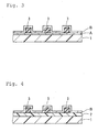
- Fig. 3 shows a second preferred embodiment of the optical waveguide according to the present invention.
- the optical waveguide according to the second preferred embodiment includes a second metal film B formed in place of the over cladding layer 4 (see Fig. 1 ) in the optical waveguide of the first preferred embodiment described above.
- Other parts of the second preferred embodiment are similar to those of the first preferred embodiment described above, and like reference numerals and characters are used to designate similar parts.
- a surface of a first metal film A and a surface of the second metal film B serve as surfaces which reflect light passing through cores 3 in portions where bottom surfaces of the cores 3 and side and top surfaces of the cores 3 are in contact with the first and second metal films A and B, respectively.
- a method of manufacturing the optical waveguide according to the second preferred embodiment includes a first step of forming the first metal film A and the cores 3 in this order [see Fig. 2(d) ] on a substrate 1 in substantially the same manner as that of.the first preferred embodiment described above [see Figs. 2(a) to 2(d) ] . Thereafter, as shown in Fig. 3 , the second metal film B is formed on the side and top surfaces of the cores 3 in substantially the same manner as that of the method of forming the first metal film A, for example, by a sputtering method, a plasma method, a chemical vapor deposition method, or a plating method.
- Examples of a material for the formation of the second metal film B are substantially the same as those for the formation of the first metal film A, such as, silver, aluminum, nickel, chromium, or copper.
- the material for the formation of the second metal film B may be the same as or different from the material for the formation of the first metal film A.
- Fig. 4 shows a third preferred embodiment of the optical waveguide according to the present invention.
- the optical waveguide according to the third preferred embodiment includes an under cladding layer 2 formed in place of the first metal film A (see Fig. 3 ) in the optical waveguide of the second preferred embodiment described above.
- Other parts of the third preferred embodiment are similar to those of the second preferred embodiment described above, and like reference numerals and characters are used to designate similar parts.
- a surface of a metal film B serves as a surface which reflects light passing through cores 3 in portions where side and top surfaces of the cores 3 are in contact with the metal film B.
- a method of manufacturing the optical waveguide according to the third preferred embodiment includes a first step of forming the under cladding layer 2 on the surface of a substrate 1, as shown in Fig. 5(a) .
- a material for the formation of the under cladding layer 2 are substantially the same as those for the formation of the over cladding layer 4 described in the first preferred embodiment [see Fig. 2 (e) ], such as, polyimideresin, epoxyresin, orphotopolymerizableresin.
- the material for the formation of the under cladding layer 2 may be the same as or different from the material for the formation of the over cladding layer 4.
- a method of forming the under cladding layer 2 is performed in substantially the same manner as that for the above-mentioned over cladding layer 4. Specifically, a varnish, which will serve as the under cladding layer 2 later, is applied onto the surface of the substrate 1 by the spin coating method or the like. Thereafter, a heating treatment is performed where a polyimide resin is used as the material for the formation of the under cladding layer 2, and a heating treatment is performed after the irradiation with ultraviolet light where a photopolymerizable resin is used as the material for the formation of the under cladding layer 2. Thus, the under cladding layer 2 is formed.
- the thickness of the under cladding layer 2 is set at 5 ⁇ m to 50 ⁇ m for a multimode optical waveguide, and is set at 1 ⁇ m to 20 ⁇ m for a single-mode optical waveguide.
- the cores 3 are formed on a surface of the under cladding layer 2 in substantially the same manner as that of the first and second preferred embodiments [see Figs. 2(b) to 2(d) ].
- a second metal film B is formed in substantially the same manner as that of the second preferred embodiment, for example, by a sputtering method, a plasma method, a chemical vapor deposition method, or a plating method. In this manner, the optical waveguide according to the third preferred embodiment is obtained.
- a material for formation of an over cladding layer was prepared by mixing 35 parts by weight of bisphenoxyethanolfluorene diglycidyl ether (component A), 40 parts by weight of (3',4'-Epoxycyclohexane)methyl 3',4'-Epoxycyclohexyl-carboxylate (component B), 25 parts by weight of an alicyclic epoxy resin (CELLOXIDE 2021P manufactured by Daicel Chemical Industries, Ltd.) (component C), and one part by weight of a 50% propione carbonate solution of 4,4-bis[di( ⁇ -hydroxyethoxy) phenylsulfinio]phenylsulfide bishexafluoroantimonate (photo-acid generator: component D).
- a material for the formation of the cores was prepared by dissolving 70 parts by weight of the above-mentioned component A, 30 parts by weight of 1, 3, 3-trisf 4-[2-(3-oxetanyl)] butoxyphenyl ⁇ butane and 0.5 part by weight of the above-mentioned component D in 28 parts by weight of ethyl lactate.
- a silver (Ag) film (having a thickness of 0.15 ⁇ m) was formed on a surface of a polyethylene naphthalate film [substrate: 100 mm ⁇ 100 mm ⁇ 188 ⁇ m (thick)] by sputtering.
- the material for the formation of the cores was applied to the surface of the silver (Ag) film by a spin coating method. Thereafter, a heating treatment was performed at 100 °C for 5 minutes .
- a translucent cover film made of polycarbonate (having a thickness of 40 ⁇ m) was placed on the surface of the material for the formation of the cores, and a synthetic silica photomask formed with an opening pattern (core pattern) was placed on the surface of the cover film. Then, irradiation with ultraviolet radiation from above was performed at 4000 mJ/cm 2 . After the photomask and the cover film were removed, a heating treatment was performed at 80°C for 15 minutes.
- the material for the formation of the over cladding layer was applied by a spin coating method so as to cover the cores, and was then exposed to ultraviolet radiation at 2000 mJ/cm 2 . Subsequently, a heating treatment was performed at 120°C for 15 minutes to form the over cladding layer (having a thickness of 70 ⁇ m as measured from the surface of the under cladding layer).
- an optical waveguide (see Fig. 1 ) including a silver (Ag) film, cores and an over cladding layer stacked in the order named on a substrate was produced.
- An optical waveguide was produced in the same way as Example 1, except that an aluminum (Al) film (having a thickness of 0.15 ⁇ m) was formed by sputtering as the metal film in place of the silver (Ag) film in Example 1.
- an optical waveguide (see Fig. 1 ) including an aluminum (Al) film, cores and an over cladding layer stacked in the order named on a substrate was produced.
- An optical waveguide was produced in the same way as Example 1, except that a second silver (Ag) film (having a thickness of 0.15 ⁇ m) was formed on side and top surfaces of cores by sputtering in place of the over cladding layer in Example 1.
- a second silver (Ag) film having a thickness of 0.15 ⁇ m
- an optical waveguide including a silver (Ag) film, cores and a second silver (Ag) film stacked in the order named on a substrate was produced.
- An optical waveguide was produced in the same way as Example 1, except that an aluminum (A1) film (having a thickness of 0.15 ⁇ m) was formed on side and top surfaces of cores by sputtering in place of the over cladding layer in Example 1.
- an optical waveguide (see Fig. 3 ) including a silver (Ag) film, cores and an aluminum (Al) film stacked in the order named on a substrate was produced.
- Example 1 a material substantially the same as that for the formation of the over cladding layer of Example 1 was applied to the surface of a polyethylene naphthalate film substantially the same as that of Example 1 by a spin coating method, and was then exposed to ultraviolet radiation at 2000 mJ/cm 2 . Subsequently, a heating treatment was performed at 100°C for 15 minutes to form an under cladding layer (having a thickness of 20 ⁇ m).
- Example 1 the material for the formation of the cores of Example 1 was applied to the surface of the under cladding layer by a spin coating method, and was then dried at 100 °C for 15 minutes.
- a translucent cover film made of polycarbonate (having a thickness of 40 ⁇ m) was placed on the surface of the dried material for the formation of cores, and a synthetic silica photomask formed with an opening pattern (core pattern) was placed on the surface of the cover film.
- exposure to ultraviolet radiation from above was performed at 4000 mJ/cm 2 .
- a heating treatment was performed at 80 °C for 15 minutes.
- a silver (Ag) film (having a thickness of 0.15 ⁇ m) was formed on the side and top surfaces of the cores by sputtering.
- an optical waveguide (see Fig. 4 ) including an under cladding layer, cores and a silver (Ag) film stacked in the order named on a substrate was produced.
Landscapes
- Physics & Mathematics (AREA)
- Engineering & Computer Science (AREA)
- Microelectronics & Electronic Packaging (AREA)
- General Physics & Mathematics (AREA)
- Optics & Photonics (AREA)
- Optical Integrated Circuits (AREA)
Abstract
Description
- The present invention relates to an optical waveguide for widespread use in optical communications, optical information processing, and other general optics.
- An optical waveguide is incorporated in an optical device such as an optical waveguide device, an optical integrated circuit, an optical wiring board and the like, and is widely used in the field of optical communications, optical information processing, and other general optics. In general, the optical waveguide includes cores serving as a passageway for light and formed in a predetermined pattern, and an under cladding layer and an over cladding layer formed so as to cover the cores (see, for example,
JP-A-2005-165138 Fig. 6 . InFig. 6 , an undercladding layer 2,cores 3, and an overcladding layer 4 are formed in the order named on asubstrate 1 to form the optical waveguide. - The refractive index of the above-mentioned
cores 3 is made higher than that of the undercladding layer 2 and the overcladding layer 4 so that light passing inside thecores 3 does not exit from thecores 3. Thecores 3, the undercladding layer 2 and the over claddinglayer 4 are in general made of a synthetic resin. In particular., when thecores 3, the undercladding layer 2 and the over claddinglayer 4 are made of a photosensitive resin, the formation thereof involves the need for the steps of coating, exposure to light, development and drying of liquid materials therefor. - However, the execution of the above-mentioned steps of coating, exposure to light, development and drying for each of the processes of forming the
cores 3, the under claddinglayer 2 and the over claddinglayer 4 described above requires a large number of processing steps to result in the increase in costs. In this regard, there is room for improvement. - In view of the foregoing, it is therefore an obj ect of the present invention to provide an optical waveguide which is capable of achieving reduction in the number of processing steps for manufacture and reduction in manufacturing costs.
- To accomplish the above-mentioned object, an optical waveguide according to the present invention comprises a core formed on a substrate and serving as a passageway for light, wherein at least a portion of the above-mentioned core is covered with a metal film.
- The optical waveguide according to the present invention, in which at least a portion of the core is covered with a metal film, eliminates the need to form a cladding layer (at least one of an under cladding layer and an over cladding layer) in that portion. The formation of the metal film may be carried out, for example, by using any one of a sputtering method, a plasma method, a chemical vapor deposition method, and a plating method. Covering of a portion of the core with the metal film can be carried out with a smaller number of processing steps than those required for the formation of a cladding layer. Accordingly, this provides reduction in the number of processing steps for manufacturing an optical waveguide and consequently provides a reduction in manufacturing costs.
-
-
Fig. 1 is a sectional view schematically showing a first preferred embodiment of an optical waveguide according to the present invention; -
Figs. 2(a) to 2(e) are sectional views schematically showing a method of manufacturing the optical waveguide of the first preferred embodiment; -
Fig. 3 is a sectional view schematically showing a second preferred embodiment of the optical waveguide according to the present invention; -
Fig. 4 is a sectional view schematically showing a third preferred embodiment of the optical waveguide according to the present invention; -
Figs. 5(a) to 5(c) are sectional views schematically showing a method of manufacturing the optical waveguide of the third preferred embodiment; and -
Fig. 6 is a sectional view schematically showing a related art optical waveguide. - Preferred embodiments of the present invention will now be described in detail with reference to the drawings.
-
Fig. 1 shows a first preferred embodiment of an optical waveguide according to the present invention. The optical waveguide according to this preferred embodiment includes a metal film A formed on a surface of asubstrate 1 of a flat shape, a plurality ofcores 3 formed in a predetermined pattern on a surface of the metal film A, and an overcladding layer 4 formed so as to cover thecores 3. The surface of the metal film A serves as a surface which reflects light passing through thecore 3 in portions where bottom surfaces of thecores 3 are in contact with the metal film A. - A method of manufacturing such an optical waveguide will be described.
- First, the
substrate 1 is prepared, as shown inFig. 2 (a) . Thesubstrate 1 employed in this embodiment is not particularly limited. Examples of thesubstrate 1 include a resin substrate, a glass substrate, and a silicon substrate. Examples of a material for the formation of the resin substrate include polyethylene naphthalate, polyester, polyacrylate, polycarbonate, polynorbornene, and polyimide. The thickness of thesubstrate 1 is not particularly limited. The thickness may be generally set within a range of 20 µm (for a substrate of a film-like configuration) to 5 mm (for a substrate of a plate-like configuration). - Next, the metal film A is formed on the surface of the
substrate 1, for example, by using any one of a sputtering method, a plasma method, a chemical vapor deposition method, and a plating method. Examples of a material for the formation of the metal film A include silver, aluminum, nickel, chromium , copper, and an alloy material including at least two of these elements. The thickness of the metal film A is not particularly limited, but is generally set within the range of 0.1 to 0.5 µm. - Next, as shown in
Fig. 2 (b) , aresin layer 3a, which will later be formed into the cores 3 [seeFig. 2(d) ] by selective exposure to radiation, is formed on the surface of the metal film A. In general, an example of a material for the formation of theresin layer 3a is a photopolymerizable resin which has a refractive index greater than that of a material for the formation of the over cladding layer 4 [seeFig. 2(e) ] to be described later. The refractive index may be adjusted, for example, by properly selecting the types of materials or adjusting the composition ratio thereof for the formation of thecores 3 and the overcladding layer 4. The method of forming theresin layer 3a is not particularly limited. Theresin layer 3a is formed by, for example, applying a varnish prepared by dissolving a photopolymerizable resin in a solvent onto the metal film A, and then drying the varnish. The varnish is applied by, for example, a spin coating method, a dipping method, a casting method, an injection method, or an ink jet method. The varnish is dried by a heat treatment, for example, at 50°C to 120°C for 10 to 30 minutes. To improve the adhesion between the metal film A and the cores 3 [seeFig. 2 (d) ], a primer resin treatment, a coupling agent treatment and the like may be performed on the surface of the metal film A prior to the formation of theresin layer 3a. - Then, as shown in
Fig. 2(c) , the surface of the driedresin layer 3a is covered with a translucent cover film C, and a photomask M formed with an opening pattern corresponding to a desired pattern of the cores 3 [seeFig. 2(d) ] is placed on the cover film C. Thereafter, theresin layer 3a is exposed to radiation through the photomask M and cover film C. Exposed portions will later serve as thecores 3. Examples of the radiation for exposure used herein include visible light, ultraviolet radiation, infrared radiation, X-rays, alpha rays, beta rays, and gamma rays. Preferably, ultraviolet radiation is used. This is because the use of ultraviolet radiation achieves exposure with large energy to provide a high rate of cure, and an irradiation apparatus therefor is small in size and inexpensive to achieve the reduction in production costs. A light source of ultraviolet radiation may be, for example, a low-pressure mercury-vapor lamp, a high-pressure mercury-vapor lamp, or an ultra-high-pressure mercury-vapor lamp. The dose of ultraviolet radiation is generally 10 mJ/cm2 to 10000 mJ/cm2, preferably 50 mJ/cm2 to 3000 mJ/cm2. - After the exposure, a heating treatment is performed to complete a photoreaction at 80°C to 250°C , preferably at 100°C to 200 °C , for 10 seconds to two hours, preferably for five minutes to one hour. Thereafter, development is performed using a developing solution to dissolve and remove an unexposed portion of the
resin layer 3a, thereby patterning theresin layer 3a [seeFig. 2 (d) ] A heating treatment is performed at 80 °C to 120 °C for 10 to 30 minutes, in general, to remove the developing solution in the patternedresin layer 3a, thereby forming the pattern of thecores 3, as shown inFig. 2(d) . In general, the thickness of each of thecores 3 is set at 20 µm to 100 µm for a multimode optical waveguide, and is set at 2 µm to 10 µm for a single-mode optical waveguide. Examples of methods of development include an immersion method, a spray method, and a puddle method. Examples of the developing solutions used herein include an organic solvent, and an organic solvent containing an alkaline aqueous solution. Suchadevelopingsolution and development conditions are selected as appropriate depending on the composition of a photopolymerizable resin composition. - Next, as shown in
Fig. 2 (e) , the overcladding layer 4 is formed so as to cover the above-mentionedcores 3. Examples of the material for the formation of the over claddinglayer 4 include polyimide resin, epoxy resin, and photopolymerizable resin. A method of forming the over claddinglayer 4 is not particularly limited, but is performed, for example, by applying a varnish prepared by dissolving any one of the above-mentioned resins in a solvent so as to cover the above-mentionedcores 3, and then curing the varnish. The varnish is applied, for example, by a spin coating method, a dipping method, a casting method, an injection method, or an ink jet method. The varnish is cured as appropriate depending on the formation material and thickness of the overcladding layer 4 and the like. For example, where a polyimide resin is used as the material for the formation of the overcladding layer 4, the curing is carried out by a heating treatment at 300 °C to 400 °C for 60 to 180 minutes. Where a photopolymerizable resin is used as the material for the formation of the overcladding layer 4, the curing is carried out by an exposure to ultraviolet radiation at 1000 mJ/cm2 to 5000 mJ/cm2 followed by a heating treatment at 80°C to 120°C for 10 to 30 minutes. In general, the thickness of the overcladding layer 4 is set at 5 µm to 100 µm for a multimode optical waveguide, and is set at 1 µm to 20 µm for a single-mode optical waveguide. - In this manner, the optical waveguide (see
Fig. 1 ) in which the metal film A, thecores 3 and the overcladding layer 4 are laminated on the surface of thesubstrate 1 is formed. - Although the over
cladding layer 4 is formed in the first preferred embodiment, the overcladding layer 4 is not essential and may be omitted in the formation of the optical waveguide in some instances. -
Fig. 3 shows a second preferred embodiment of the optical waveguide according to the present invention. The optical waveguide according to the second preferred embodiment includes a second metal film B formed in place of the over cladding layer 4 (seeFig. 1 ) in the optical waveguide of the first preferred embodiment described above. Other parts of the second preferred embodiment are similar to those of the first preferred embodiment described above, and like reference numerals and characters are used to designate similar parts. In the optical waveguide of the second preferred embodiment, a surface of a first metal film A and a surface of the second metal film B serve as surfaces which reflect light passing throughcores 3 in portions where bottom surfaces of thecores 3 and side and top surfaces of thecores 3 are in contact with the first and second metal films A and B, respectively. - A method of manufacturing the optical waveguide according to the second preferred embodiment includes a first step of forming the first metal film A and the
cores 3 in this order [seeFig. 2(d) ] on asubstrate 1 in substantially the same manner as that of.the first preferred embodiment described above [seeFigs. 2(a) to 2(d) ] . Thereafter, as shown inFig. 3 , the second metal film B is formed on the side and top surfaces of thecores 3 in substantially the same manner as that of the method of forming the first metal film A, for example, by a sputtering method, a plasma method, a chemical vapor deposition method, or a plating method. Examples of a material for the formation of the second metal film B are substantially the same as those for the formation of the first metal film A, such as, silver, aluminum, nickel, chromium, or copper. The material for the formation of the second metal film B may be the same as or different from the material for the formation of the first metal film A. Thus, the optical waveguide according to the second preferred embodiment is obtained. -
Fig. 4 shows a third preferred embodiment of the optical waveguide according to the present invention. The optical waveguide according to the third preferred embodiment includes an undercladding layer 2 formed in place of the first metal film A (seeFig. 3 ) in the optical waveguide of the second preferred embodiment described above. Other parts of the third preferred embodiment are similar to those of the second preferred embodiment described above, and like reference numerals and characters are used to designate similar parts. In the optical waveguide of the third preferred embodiment, a surface of a metal film B serves as a surface which reflects light passing throughcores 3 in portions where side and top surfaces of thecores 3 are in contact with the metal film B. - A method of manufacturing the optical waveguide according to the third preferred embodiment includes a first step of forming the under
cladding layer 2 on the surface of asubstrate 1, as shown inFig. 5(a) . Examples of a material for the formation of theunder cladding layer 2 are substantially the same as those for the formation of the overcladding layer 4 described in the first preferred embodiment [seeFig. 2 (e) ], such as, polyimideresin, epoxyresin, orphotopolymerizableresin. The material for the formation of theunder cladding layer 2 may be the same as or different from the material for the formation of the overcladding layer 4. A method of forming the undercladding layer 2 is performed in substantially the same manner as that for the above-mentioned overcladding layer 4. Specifically, a varnish, which will serve as the undercladding layer 2 later, is applied onto the surface of thesubstrate 1 by the spin coating method or the like. Thereafter, a heating treatment is performed where a polyimide resin is used as the material for the formation of theunder cladding layer 2, and a heating treatment is performed after the irradiation with ultraviolet light where a photopolymerizable resin is used as the material for the formation of theunder cladding layer 2. Thus, the undercladding layer 2 is formed. In general, the thickness of theunder cladding layer 2 is set at 5 µm to 50 µm for a multimode optical waveguide, and is set at 1 µm to 20 µm for a single-mode optical waveguide. Next, as shown inFig. 5 (b) , thecores 3 are formed on a surface of theunder cladding layer 2 in substantially the same manner as that of the first and second preferred embodiments [seeFigs. 2(b) to 2(d) ]. Thereafter, as shown inFig. 5 (c) , a second metal film B is formed in substantially the same manner as that of the second preferred embodiment, for example, by a sputtering method, a plasma method, a chemical vapor deposition method, or a plating method. In this manner, the optical waveguide according to the third preferred embodiment is obtained. - Next, inventive examples will be described. It should be noted that the present invention is not limited to the inventive examples.
- A material for formation of an over cladding layer was prepared by mixing 35 parts by weight of bisphenoxyethanolfluorene diglycidyl ether (component A), 40 parts by weight of (3',4'-Epoxycyclohexane)methyl 3',4'-Epoxycyclohexyl-carboxylate (component B), 25 parts by weight of an alicyclic epoxy resin (CELLOXIDE 2021P manufactured by Daicel Chemical Industries, Ltd.) (component C), and one part by weight of a 50% propione carbonate solution of 4,4-bis[di(β-hydroxyethoxy) phenylsulfinio]phenylsulfide bishexafluoroantimonate (photo-acid generator: component D).
- A material for the formation of the cores was prepared by dissolving 70 parts by weight of the above-mentioned component A, 30 parts by weight of 1, 3, 3-trisf 4-[2-(3-oxetanyl)] butoxyphenyl} butane and 0.5 part by weight of the above-mentioned component D in 28 parts by weight of ethyl lactate.
- First, a silver (Ag) film (having a thickness of 0.15 µm) was formed on a surface of a polyethylene naphthalate film [substrate: 100 mm × 100 mm × 188 µm (thick)] by sputtering.
- Then, the material for the formation of the cores was applied to the surface of the silver (Ag) film by a spin coating method. Thereafter, a heating treatment was performed at 100 °C for 5 minutes . Next, a translucent cover film made of polycarbonate (having a thickness of 40 µm) was placed on the surface of the material for the formation of the cores, and a synthetic silica photomask formed with an opening pattern (core pattern) was placed on the surface of the cover film. Then, irradiation with ultraviolet radiation from above was performed at 4000 mJ/cm2. After the photomask and the cover film were removed, a heating treatment was performed at 80°C for 15 minutes. Next, development was carried out using an aqueous solution of γ -butyrolactone to dissolve and remove an unexposed portion. Thereafter, a heating treatment was performed at 100 °C for 15 minutes to form the cores (having a thickness of 50 µm).
- Next, the material for the formation of the over cladding layer was applied by a spin coating method so as to cover the cores, and was then exposed to ultraviolet radiation at 2000 mJ/cm2. Subsequently, a heating treatment was performed at 120°C for 15 minutes to form the over cladding layer (having a thickness of 70 µm as measured from the surface of the under cladding layer).
- In this manner, an optical waveguide (see
Fig. 1 ) including a silver (Ag) film, cores and an over cladding layer stacked in the order named on a substrate was produced. - An optical waveguide was produced in the same way as Example 1, except that an aluminum (Al) film (having a thickness of 0.15 µm) was formed by sputtering as the metal film in place of the silver (Ag) film in Example 1. Thus, an optical waveguide (see
Fig. 1 ) including an aluminum (Al) film, cores and an over cladding layer stacked in the order named on a substrate was produced. - An optical waveguide was produced in the same way as Example 1, except that a second silver (Ag) film (having a thickness of 0.15 µm) was formed on side and top surfaces of cores by sputtering in place of the over cladding layer in Example 1. Thus, an optical waveguide (see
Fig. 3 ) including a silver (Ag) film, cores and a second silver (Ag) film stacked in the order named on a substrate was produced. - An optical waveguide was produced in the same way as Example 1, except that an aluminum (A1) film (having a thickness of 0.15 µm) was formed on side and top surfaces of cores by sputtering in place of the over cladding layer in Example 1. Thus, an optical waveguide (see
Fig. 3 ) including a silver (Ag) film, cores and an aluminum (Al) film stacked in the order named on a substrate was produced. - First, a material substantially the same as that for the formation of the over cladding layer of Example 1 was applied to the surface of a polyethylene naphthalate film substantially the same as that of Example 1 by a spin coating method, and was then exposed to ultraviolet radiation at 2000 mJ/cm2. Subsequently, a heating treatment was performed at 100°C for 15 minutes to form an under cladding layer (having a thickness of 20 µm).
- Then, the material for the formation of the cores of Example 1 was applied to the surface of the under cladding layer by a spin coating method, and was then dried at 100 °C for 15 minutes. Next, a translucent cover film made of polycarbonate (having a thickness of 40 µm) was placed on the surface of the dried material for the formation of cores, and a synthetic silica photomask formed with an opening pattern (core pattern) was placed on the surface of the cover film. Then, exposure to ultraviolet radiation from above was performed at 4000 mJ/cm2. After the photomask and the cover film were removed, a heating treatment was performed at 80 °C for 15 minutes. Next, development was carried out using an aqueous solution of γ-butyrolactone to dissolve and remove an unexposed portion. Thereafter, a heating treatment was performed at 100 °C for 15 minutes to form the cores (having a thickness of 50 µm).
- Then, a silver (Ag) film (having a thickness of 0.15 µm) was formed on the side and top surfaces of the cores by sputtering.
- Thus, an optical waveguide (see
Fig. 4 ) including an under cladding layer, cores and a silver (Ag) film stacked in the order named on a substrate was produced. - Although specific forms of embodiments of the instant invention have been described above and illustrated in the accompanying drawings in order to be more clearly understood, the above description is made by way of examples and not as a limitation to the scope of the instant invention. It is contemplated that various modifications apparent to one of ordinary skill in the art could be made without departing from the scope of the invention which is to be determined by the following claims.
Claims (4)
- An optical waveguide comprising:a substrate;a core formed on the substrate and serving as a passageway for light; anda metal film,wherein at least a portion of said core is covered with said metal film.
- The optical waveguide according to claim 1, wherein said metal film is formed on a surface of said substrate, wherein said core is formed such that a bottom surface thereof is in contact with said metal film.
- The optical waveguide according to claim 2, further comprising a second metal film for covering side and top surfaces of said core.
- The optical waveguide according to claim 1, further comprising an under cladding layer formed on a surface of said substrate, wherein said core is formed on a surface of said under cladding layer such that a bottom surface of said core is in contact with said under cladding layer, wherein said metal film is formed such that side and top surfaces of said core is covered with said metal film.
Applications Claiming Priority (1)
| Application Number | Priority Date | Filing Date | Title |
|---|---|---|---|
| JP2007120892A JP2008276000A (en) | 2007-05-01 | 2007-05-01 | Optical waveguide |
Publications (1)
| Publication Number | Publication Date |
|---|---|
| EP1988414A1 true EP1988414A1 (en) | 2008-11-05 |
Family
ID=39688860
Family Applications (1)
| Application Number | Title | Priority Date | Filing Date |
|---|---|---|---|
| EP08007631A Withdrawn EP1988414A1 (en) | 2007-05-01 | 2008-04-18 | Optical waveguide |
Country Status (5)
| Country | Link |
|---|---|
| US (1) | US7711230B2 (en) |
| EP (1) | EP1988414A1 (en) |
| JP (1) | JP2008276000A (en) |
| KR (1) | KR20080097337A (en) |
| CN (1) | CN101299080A (en) |
Cited By (1)
| Publication number | Priority date | Publication date | Assignee | Title |
|---|---|---|---|---|
| WO2017039824A1 (en) * | 2015-09-04 | 2017-03-09 | Raytheon Company | Techniques for forming waveguides for use in laser systems or other systems and associated devices |
Families Citing this family (11)
| Publication number | Priority date | Publication date | Assignee | Title |
|---|---|---|---|---|
| KR100936345B1 (en) * | 2003-09-01 | 2010-01-12 | 엘지이노텍 주식회사 | Optical splitter and its manufacturing method |
| KR200433253Y1 (en) * | 2006-09-15 | 2006-12-08 | 이부규 | Ventilator cover combined with lighting |
| JP4934069B2 (en) * | 2008-01-24 | 2012-05-16 | 日東電工株式会社 | Manufacturing method of opto-electric hybrid board |
| JP4934068B2 (en) * | 2008-01-24 | 2012-05-16 | 日東電工株式会社 | Manufacturing method of opto-electric hybrid board and opto-electric hybrid board obtained thereby |
| JP2010282080A (en) * | 2009-06-05 | 2010-12-16 | Nitto Denko Corp | Manufacturing method of optical waveguide |
| US8428401B2 (en) * | 2009-12-16 | 2013-04-23 | Telefonaktiebolaget L M Ericsson (Publ) | On-chip optical waveguide |
| CN102316662A (en) * | 2010-06-29 | 2012-01-11 | 欣兴电子股份有限公司 | Photoelectric circuit board and manufacturing method thereof |
| US8837872B2 (en) * | 2010-12-30 | 2014-09-16 | Qualcomm Incorporated | Waveguide structures for signal and/or power transmission in a semiconductor device |
| KR20120139264A (en) * | 2011-06-17 | 2012-12-27 | 한국전자통신연구원 | Apparatus for sensing pressure using optical waveguide and method thereof |
| US10302847B2 (en) | 2015-05-22 | 2019-05-28 | Microsoft Technology Licensing, Llc | Micro injection-molded articles |
| US11275208B2 (en) * | 2018-02-26 | 2022-03-15 | Arizona Board Of Regents On Behalf Of The University Of Arizona | Fabrication of polymer waveguide interconnect between chips with a gap and/or step |
Citations (4)
| Publication number | Priority date | Publication date | Assignee | Title |
|---|---|---|---|---|
| US3563630A (en) * | 1966-12-07 | 1971-02-16 | North American Rockwell | Rectangular dielectric optical wave-guide of width about one-half wave-length of the transmitted light |
| US4376160A (en) * | 1980-04-07 | 1983-03-08 | California Institute Of Technology | Method of making and structure for monolithic optical circuits |
| JP2003043281A (en) * | 2001-07-26 | 2003-02-13 | Kyocera Chemical Corp | Optical wave guide circuit and method for manufacturing the same |
| JP2005165138A (en) | 2003-12-04 | 2005-06-23 | Nitto Denko Corp | Optical waveguide |
Family Cites Families (13)
| Publication number | Priority date | Publication date | Assignee | Title |
|---|---|---|---|---|
| US5659648A (en) * | 1995-09-29 | 1997-08-19 | Motorola, Inc. | Polyimide optical waveguide having electrical conductivity |
| US6954561B1 (en) * | 2001-07-16 | 2005-10-11 | Applied Materials Inc | Methods for forming thermo-optic switches, routers and attenuators |
| JP2003121668A (en) * | 2001-10-16 | 2003-04-23 | Dainippon Printing Co Ltd | Optical waveguide and method for manufacturing the same |
| JP3786858B2 (en) * | 2001-10-16 | 2006-06-14 | 大日本印刷株式会社 | Optical waveguide and method for manufacturing the same |
| WO2003038491A1 (en) * | 2001-11-02 | 2003-05-08 | Imego Ab | Conductor arrangement |
| JP3846284B2 (en) * | 2001-11-26 | 2006-11-15 | 株式会社トッパンNecサーキットソリューションズ | Manufacturing method of optical waveguide |
| US7146086B2 (en) * | 2003-06-30 | 2006-12-05 | Intel Corporation | Constructing well structures for hybrid optical waveguides |
| JP2005148468A (en) * | 2003-11-17 | 2005-06-09 | Sony Corp | Optical waveguide, light source module, and optical information processing apparatus |
| JP4318036B2 (en) * | 2004-02-16 | 2009-08-19 | オムロン株式会社 | Optical waveguide |
| KR100606549B1 (en) * | 2004-07-01 | 2006-08-01 | 엘지전자 주식회사 | Light guide plate for surface light emitting device and manufacturing method thereof |
| US7532790B2 (en) * | 2006-03-29 | 2009-05-12 | 3M Innovative Properties Company | Method of coupling light into microresonators |
| KR100851973B1 (en) * | 2006-11-02 | 2008-08-12 | 삼성전자주식회사 | waveguide, method of fabricating the same, light delivery module employing the waveguide and heat assisted magnetic recording head employing the bending waveguide |
| JP2008181411A (en) * | 2007-01-25 | 2008-08-07 | Nitto Denko Corp | Optical waveguide for touch panel |
-
2007
- 2007-05-01 JP JP2007120892A patent/JP2008276000A/en active Pending
-
2008
- 2008-04-11 KR KR1020080033542A patent/KR20080097337A/en not_active Withdrawn
- 2008-04-18 EP EP08007631A patent/EP1988414A1/en not_active Withdrawn
- 2008-04-22 CN CNA2008100953030A patent/CN101299080A/en active Pending
- 2008-05-01 US US12/113,412 patent/US7711230B2/en not_active Expired - Fee Related
Patent Citations (4)
| Publication number | Priority date | Publication date | Assignee | Title |
|---|---|---|---|---|
| US3563630A (en) * | 1966-12-07 | 1971-02-16 | North American Rockwell | Rectangular dielectric optical wave-guide of width about one-half wave-length of the transmitted light |
| US4376160A (en) * | 1980-04-07 | 1983-03-08 | California Institute Of Technology | Method of making and structure for monolithic optical circuits |
| JP2003043281A (en) * | 2001-07-26 | 2003-02-13 | Kyocera Chemical Corp | Optical wave guide circuit and method for manufacturing the same |
| JP2005165138A (en) | 2003-12-04 | 2005-06-23 | Nitto Denko Corp | Optical waveguide |
Non-Patent Citations (1)
| Title |
|---|
| KAMINOW I P ET AL: "Metal-clad optical waveguides: analytical and experimental study", APPLIED OPTICS, vol. 13, no. 2, February 1974 (1974-02-01), pages 396 - 405, XP002492897, ISSN: 0003-6935 * |
Cited By (3)
| Publication number | Priority date | Publication date | Assignee | Title |
|---|---|---|---|---|
| WO2017039824A1 (en) * | 2015-09-04 | 2017-03-09 | Raytheon Company | Techniques for forming waveguides for use in laser systems or other systems and associated devices |
| IL255849A (en) * | 2015-09-04 | 2018-01-31 | Raytheon Co | Techniques for forming waveguides for use in laser systems or other systems and associated devices |
| US10203461B2 (en) | 2015-09-04 | 2019-02-12 | Raytheon Company | Techniques for forming waveguides for use in laser systems or other systems and associated devices |
Also Published As
| Publication number | Publication date |
|---|---|
| US20080273853A1 (en) | 2008-11-06 |
| KR20080097337A (en) | 2008-11-05 |
| CN101299080A (en) | 2008-11-05 |
| JP2008276000A (en) | 2008-11-13 |
| US7711230B2 (en) | 2010-05-04 |
Similar Documents
| Publication | Publication Date | Title |
|---|---|---|
| US7711230B2 (en) | Optical waveguide | |
| US7989150B2 (en) | Manufacturing method of optical waveguide | |
| EP1990664A2 (en) | Manufacturing method of optical waveguide | |
| EP2058728B1 (en) | Optical waveguide for touch screen and touch screen using the same | |
| EP2083295B1 (en) | Manufacturing method of opto-electric hybrid board and opto-electric hybrid board obtained thereby | |
| EP2023174A1 (en) | Optical waveguide device and manufacturing method thereof | |
| EP2083294B1 (en) | Manufacturing method of opto-electric hybrid board and opto-electric hybrid board obtained thereby | |
| EP2075676A2 (en) | Optical waveguide for touch panel, touch panel using the optical waveguide and manufacturing method of the optical waveguide | |
| KR20090050959A (en) | Optical waveguide device for touch panel and touch panel using the same | |
| KR20090120406A (en) | Manufacturing method of optical waveguide device | |
| JP2012093563A (en) | Method of manufacturing optical waveguide for touch panel | |
| EP2058686A1 (en) | Manufacturing method of optical waveguide device and optical waveguide device obtained thereby | |
| US7587114B2 (en) | Film-shaped optical waveguide production method | |
| EP2163925A2 (en) | Manufacturing method of optical waveguide on a irradiation light absorbing substrate | |
| JP2009015307A (en) | Manufacturing method of optical waveguide | |
| US7587119B2 (en) | Optical waveguide device | |
| US20080274273A1 (en) | Manufacturing method of optical waveguide | |
| JP2008129332A (en) | Manufacturing method of optical waveguide |
Legal Events
| Date | Code | Title | Description |
|---|---|---|---|
| PUAI | Public reference made under article 153(3) epc to a published international application that has entered the european phase |
Free format text: ORIGINAL CODE: 0009012 |
|
| AK | Designated contracting states |
Kind code of ref document: A1 Designated state(s): AT BE BG CH CY CZ DE DK EE ES FI FR GB GR HR HU IE IS IT LI LT LU LV MC MT NL NO PL PT RO SE SI SK TR |
|
| AX | Request for extension of the european patent |
Extension state: AL BA MK RS |
|
| 17P | Request for examination filed |
Effective date: 20090506 |
|
| AKX | Designation fees paid |
Designated state(s): DE GB |
|
| 17Q | First examination report despatched |
Effective date: 20110113 |
|
| STAA | Information on the status of an ep patent application or granted ep patent |
Free format text: STATUS: THE APPLICATION IS DEEMED TO BE WITHDRAWN |
|
| 18D | Application deemed to be withdrawn |
Effective date: 20121031 |