EP1983572A1 - Transformer based ESD protection - Google Patents
Transformer based ESD protection Download PDFInfo
- Publication number
- EP1983572A1 EP1983572A1 EP07106538A EP07106538A EP1983572A1 EP 1983572 A1 EP1983572 A1 EP 1983572A1 EP 07106538 A EP07106538 A EP 07106538A EP 07106538 A EP07106538 A EP 07106538A EP 1983572 A1 EP1983572 A1 EP 1983572A1
- Authority
- EP
- European Patent Office
- Prior art keywords
- inductor
- esd
- circuit
- analog circuit
- gate
- Prior art date
- Legal status (The legal status is an assumption and is not a legal conclusion. Google has not performed a legal analysis and makes no representation as to the accuracy of the status listed.)
- Withdrawn
Links
- 238000000034 method Methods 0.000 claims abstract description 24
- 230000008878 coupling Effects 0.000 claims abstract description 14
- 238000010168 coupling process Methods 0.000 claims abstract description 14
- 238000005859 coupling reaction Methods 0.000 claims abstract description 14
- 230000015556 catabolic process Effects 0.000 claims description 8
- 238000004458 analytical method Methods 0.000 description 4
- 238000005516 engineering process Methods 0.000 description 4
- 230000010355 oscillation Effects 0.000 description 4
- 230000003071 parasitic effect Effects 0.000 description 4
- 238000013459 approach Methods 0.000 description 3
- 239000003990 capacitor Substances 0.000 description 3
- 229910052751 metal Inorganic materials 0.000 description 3
- 239000002184 metal Substances 0.000 description 3
- 230000008901 benefit Effects 0.000 description 2
- 238000001000 micrograph Methods 0.000 description 2
- 238000000926 separation method Methods 0.000 description 2
- XUIMIQQOPSSXEZ-UHFFFAOYSA-N Silicon Chemical compound [Si] XUIMIQQOPSSXEZ-UHFFFAOYSA-N 0.000 description 1
- 229910052782 aluminium Inorganic materials 0.000 description 1
- XAGFODPZIPBFFR-UHFFFAOYSA-N aluminium Chemical compound [Al] XAGFODPZIPBFFR-UHFFFAOYSA-N 0.000 description 1
- 238000010420 art technique Methods 0.000 description 1
- 230000009286 beneficial effect Effects 0.000 description 1
- 238000006243 chemical reaction Methods 0.000 description 1
- 230000007423 decrease Effects 0.000 description 1
- 238000006731 degradation reaction Methods 0.000 description 1
- 230000000694 effects Effects 0.000 description 1
- 230000001939 inductive effect Effects 0.000 description 1
- 238000005259 measurement Methods 0.000 description 1
- 230000007246 mechanism Effects 0.000 description 1
- 230000010349 pulsation Effects 0.000 description 1
- 229910052710 silicon Inorganic materials 0.000 description 1
- 239000010703 silicon Substances 0.000 description 1
Images



Classifications
-
- H—ELECTRICITY
- H10—SEMICONDUCTOR DEVICES; ELECTRIC SOLID-STATE DEVICES NOT OTHERWISE PROVIDED FOR
- H10D—INORGANIC ELECTRIC SEMICONDUCTOR DEVICES
- H10D89/00—Aspects of integrated devices not covered by groups H10D84/00 - H10D88/00
- H10D89/60—Integrated devices comprising arrangements for electrical or thermal protection, e.g. protection circuits against electrostatic discharge [ESD]
- H10D89/601—Integrated devices comprising arrangements for electrical or thermal protection, e.g. protection circuits against electrostatic discharge [ESD] for devices having insulated gate electrodes, e.g. for IGFETs or IGBTs
-
- H—ELECTRICITY
- H03—ELECTRONIC CIRCUITRY
- H03F—AMPLIFIERS
- H03F1/00—Details of amplifiers with only discharge tubes, only semiconductor devices or only unspecified devices as amplifying elements
- H03F1/08—Modifications of amplifiers to reduce detrimental influences of internal impedances of amplifying elements
- H03F1/22—Modifications of amplifiers to reduce detrimental influences of internal impedances of amplifying elements by use of cascode coupling, i.e. earthed cathode or emitter stage followed by earthed grid or base stage respectively
- H03F1/223—Modifications of amplifiers to reduce detrimental influences of internal impedances of amplifying elements by use of cascode coupling, i.e. earthed cathode or emitter stage followed by earthed grid or base stage respectively with MOSFET's
-
- H—ELECTRICITY
- H03—ELECTRONIC CIRCUITRY
- H03F—AMPLIFIERS
- H03F1/00—Details of amplifiers with only discharge tubes, only semiconductor devices or only unspecified devices as amplifying elements
- H03F1/52—Circuit arrangements for protecting such amplifiers
- H03F1/523—Circuit arrangements for protecting such amplifiers for amplifiers using field-effect devices
-
- H—ELECTRICITY
- H03—ELECTRONIC CIRCUITRY
- H03F—AMPLIFIERS
- H03F3/00—Amplifiers with only discharge tubes or only semiconductor devices as amplifying elements
- H03F3/189—High-frequency amplifiers, e.g. radio frequency amplifiers
- H03F3/19—High-frequency amplifiers, e.g. radio frequency amplifiers with semiconductor devices only
-
- H—ELECTRICITY
- H03—ELECTRONIC CIRCUITRY
- H03F—AMPLIFIERS
- H03F2200/00—Indexing scheme relating to amplifiers
- H03F2200/294—Indexing scheme relating to amplifiers the amplifier being a low noise amplifier [LNA]
-
- H—ELECTRICITY
- H03—ELECTRONIC CIRCUITRY
- H03F—AMPLIFIERS
- H03F2200/00—Indexing scheme relating to amplifiers
- H03F2200/451—Indexing scheme relating to amplifiers the amplifier being a radio frequency amplifier
-
- H—ELECTRICITY
- H03—ELECTRONIC CIRCUITRY
- H03F—AMPLIFIERS
- H03F2200/00—Indexing scheme relating to amplifiers
- H03F2200/492—A coil being added in the source circuit of a transistor amplifier stage as degenerating element
-
- H—ELECTRICITY
- H03—ELECTRONIC CIRCUITRY
- H03F—AMPLIFIERS
- H03F2200/00—Indexing scheme relating to amplifiers
- H03F2200/534—Transformer coupled at the input of an amplifier
-
- H—ELECTRICITY
- H03—ELECTRONIC CIRCUITRY
- H03F—AMPLIFIERS
- H03F2200/00—Indexing scheme relating to amplifiers
- H03F2200/541—Transformer coupled at the output of an amplifier
Definitions
- the invention relates to electrostatic discharge (ESD) protected circuits such as RF circuitry and the method for designing such circuits.
- ESD electrostatic discharge
- CMOS complementary metal-oxide-semiconductor
- I/O pins For scaled CMOS such as 45 nm and below, the oxide breakdown voltage decreases as the gate oxide becomes thinner.
- a classical dual-diode ESD protection requires larger input diodes lowering the diode turn-on resistance sufficiently to obtain the necessary ESD protection level. This increases the parasitic diode capacitance and narrows the design window for RF circuit designers significantly.
- ESD protection elements There are two approaches to implement ESD protection elements: co-design and plug&play design.
- plug&play design approach one designs a separate block comprising elements which meet with the desired ESD performance and plug it to the analog circuit.
- co-design approach the circuit that needs to be protected and the ESD elements are modeled together. Both the ESD and analog characteristics are taken into account.
- An example to protect a low noise amplifier (LNA) from ESD is shown in fig.1 .
- An inductive ESD protection consists of an inductor L ESD ( 1 ) sinking the low-frequency ESD currents (below 1 GHz) to ground, preventing the vulnerable gate of the input transistor to be damaged.
- a series capacitor C ESD ( 2 ) passes the RF signal at the LNA's operating frequency. This technique has proven to offer excellent protection (more than 2 kV HBM in 90 nm RF CMOS). For very high ESD currents, however, a residual voltage overshoot is passed on to the gate via C ESD , and the input transistor fails. This can be prevented by adding tiny clamping diodes at the gate, clipping small voltage overshoots and increasing the protection level above 5 kV HBM.
- a method for co-designing an electrostatic discharge (ESD) protection circuit with an analog circuit comprises a plurality of functional components with predetermined electric properties for achieving a predetermined analog performance. At least one of the functional components is an inductor.
- the method comprises the steps of coupling an ESD inductor with the inductor such that an ESD transformer is formed providing ESD protection to the analog circuit.
- ESD protection can be provided without area penalty.
- An analysis of the prior art has shown techniques where extra inductors are added to the circuitry. Inductors have the disadvantage that they are hard to scale down. Therefore these techniques suffer a severe area penalty. This is undesirable in expensive downscaled CMOS.
- the inductor is present at the input or at the output of the analog circuit.
- the inductors forming the ESD transformer are designed within a common area.
- the ESD inductor can for example be designed on top of the inductor of the analog circuit.
- the inductors are interwinded. In this way, substantially no area is added to the circuit by the ESD protection. Furthermore, a galvanic separation is realized between the input and the actual input of the analog circuit, heavily attenuating the possible residual voltage overshoot at the input for the ESD frequency range, and thus increasing the protection level.
- the method for co-designing an ESD protection preferably comprises the step of selecting the properties of the ESD inductor such that influence on the predetermined analog performance during normal operation is minimized.
- the analog circuit is a low noise amplifier (LNA) wherein the inductor is represented by an LNA input inductor.
- LNA low noise amplifier
- an LNA can be designed with ESD protection substantially without area penalty which is an important asset in deep-submicron CMOS design.
- the analog circuit is a power amplifier.
- the power amplifier has a resonant load comprising an inductor.
- a transformer coupling creates a matching network for the off chip load, and functions as ESD protection via an ESD inductor.
- the analog circuit is an oscillator.
- This oscillator is preferably a power oscillator based on an LC resonant LOAD, comprising an inductor.
- An oscillation signal can be brought off chip using a transformer coupling. This transformer forms both the resonant tank for oscillation, the matching network to drive the off-chip output load, and serves as ESD protection circuit via an ESD inductor.
- the analog circuit designed according to the invention comprises in combination a plurality of interconnected functional components with predetermined electric properties for achieving a predetermined analog performance during normal operation of the circuit.
- At least one of the functional components is an inductor.
- This inductor is preferably present at the input or at the output of the analog circuit.
- an ESD inductor is coupled to this inductor forming an ESD transformer providing ESD protection to the circuit.
- the circuit is a low noise amplifier circuit.
- the circuit comprises a first transistor.
- This transistor has a source, a drain, a gate, and a gate oxide separating the gate from the source and the drain.
- This transistor is one of the functional components of the circuit.
- an LNA input inductor is connected to the gate of the transistor (or gate inductor).
- An ESD inductor is coupled with the LNA input inductor such that an ESD transformer is formed providing ESD protection to avoid breakdown at said gate oxide during an ESD event.
- the circuit can be a power amplifier.
- the circuit comprises a transistor having a source, a drain, a gate and a gate oxide separating the gate from the source and the drain. This transistor forms one of the functional components of the circuit.
- the power amplifier comprises a resonant load which comprises a power amplifier output inductor connected with the drain of the transistor. An ESD inductor is being coupled with this power amplifier output inductor such that an ESD transformer is formed providing ESD protection to avoid breakdown at the output of said power amplifier during an ESD event.
- the circuit can be an oscillator.
- the circuit comprises a transistor having a source, a drain, a gate and a gate oxide separating the gate from the source and the drain. This transistor forms one of the functional components of the circuit.
- the oscillator comprises an LC resonant load comprising an oscillator inductor which is being connected with the drain of the transistor.
- An ESD inductor is coupled with the oscillator inductor such that an ESD transformer is formed providing ESD protection to avoid breakdown at the output of the oscillator during an ESD event.
- Fig.1 shows a classical inductor-based ESD protection.
- Fig.2 shows an example of the proposed low-area transformer-based ESD protection applied in an LNA.
- Fig.3 shows an Equivalent LNA input network referred to the secondary side, for a high k-value.
- Fig.4 shows transformer geometry
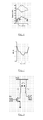
- Fig.5 represents schematic a chip micrograph.
- Fig.6 shows a plot of the measured S-parameters.
- Fig.7 shows a plot of the noise figure.
- Fig.8 shows an example of the proposed low-area transformer-based ESD protection applied in a power amplifier.
- Fig.9 shows an example of the proposed low-area transformer-based ESD protection applied in an oscillator.
- the present invention relates to a method for co-designing an electrostatic discharge (ESD) protection circuit with an analog circuit.
- the analog circuit comprises at least one functional inductor at the input or output. Possible examples of analog circuits containing such inductor at the input or the output are a LNA, a power amplifier and an oscillator.
- the method comprises the step of coupling a second inductor or ESD inductor with the inductor present at the input and/or at the output of the circuit. By coupling both inductors, a transformer is formed.
- the ESD inductor is shifted physically 'under' the inductor present (or placed above the inductor).
- the benefit is twofold. First, there is no area penalty for the ESD protection. Secondly, a galvanic separation is realized between the input and the actual input of the analog circuit, heavily attenuating the possible residual voltage overshoot at the input for the ESD frequency range, and thus increasing the protection level.
- the present invention is exemplified by means of a LNA.
- the ESD inductor, L 1 ( 11 ) is shifted under the gate inductor L G ( 12 ) already present, forming a transformer with coupling coefficient k.
- the input impedance is approximately Z IN ⁇ ⁇ T ⁇ L S n 2
- Fig.3 shows an equivalent LNA input network referred to the secondary side, for a high k -value.
- An equivalent of the primary side of the transformer, respectively secondary is represented by (33), respectively ( 32 ).
- Both blocks comprise a parasitic resistance, n 2 R 1 respectively R 2 , and a noise current, I n,R1 respectively I n,R2 .
- the parasitic resistance ( 34 ) equals n 2 R S .
- the right block of fig.3 represents the equivalent network of the transistor ( 14 ) of fig.1 .
- the method used for the noise analysis can be found in D.K. Shaeffer, T.H.
- the circuit has been designed for 5-6 GHz operation in a 0.13 ⁇ m CMOS technology. During design a trade-off has been made between noise degradation, minimum resistance in the ESD path, and acceptable power consumption.
- the transformer ( 41 ) is shown in fig.4 . It is designed as two inductors on top of each other, a primary ( 42 ) and secondary inductor ( 43 ). This eases the desired turn ratio n selection. A turn ratio n of 1.6 and a coupling factor k of 0.82 are achieved.
- the secondary is designed in the lowest resistance metal layer (M8: top metal) with an aluminum (Al) overpass.
- M8 top metal
- Al aluminum
- the Al layer 1.5 ⁇ m thick
- the Al layer (1.5 ⁇ m thick) is used as a capping layer for bondpads or for connecting the MiM-capacitors and is suitable for partial inductor layouting.
- the primary inductor (lowest number of turns) is drawn in metal 7 (M7) with M6 underpass. Its tracks are wider for low parasitic resistance and to achieve a similar resonance frequency as the secondary.
- Fig.5 shows a chip micrograph. The circuit only occupies the area needed by the three inductors present in a standard LNA design.
- Fig.6 shows the measured S-parameters of the LNA.
- the circuit has a return loss S 11 ( 61 ) below -10 dB and offers 12 dB power gain ( 62 ), driving 50 ⁇ via a tapped capacitor output match.
- On-wafer HBM measurements reveal an excellent ESD protection level of more than 8 kV positive and 5 kV negative for the input.
- the noise figure plotted in fig.7 is very respectable especially given the extremely high ESD protection level and the low area consumption. These demands - usually conflicting - are reconciled by the present invention proposed technique.
- the measured IIP3 of the LNA is -9 dBm.
- Table 1 compares the results of the present invention to the state-of-the-art of fully integrated ESD protected CMOS LNAs (no off-chip components). The present invention offers the best RF performance for excellent ESD protection and compact area.
- Table 1 - Overview of fully integrated ESD protected LNAs Present invention [1] [2] Technology (CMOS) .13 ⁇ m 90nm .18 ⁇ m f 0 (GHz) 5.5 5 5.25 NF (dB) 2.5 3.4 3.12 Power (mW) 6.6 9 10.8 Gain (dB) 12.4 12 12.41 IIP3 (dBm) -9 0.4 -14.6 HBM protection (kV) 5 5.5 ⁇ 3.4 (5.1 A TLP) Approx.
- Another application is a power amplifier or a resonant output buffer, shown in fig.8 .
- An amplifier with a resonant load including L 1 ( 81 ) amplifies the signal at node IN.
- a transformer coupling creates a matching network for the off chip load, and functions as ESD protection via L 2 ( 82 ).
- L 2 serves both as RF and ESD protection device.
- Fig.9 shows another application, a power oscillator based on an LC resonant LOAD, comprising an inductor L 1 ( 91 ) .
- An example is the Collpits oscillator.
- An oscillation is present at node V osc ( 93 ).
- This signal can be brought off chip using a transformer coupling. This transformer forms both the resonant tank for oscillation, the matching network to drive the off-chip output load, and serves as ESD protection via L 2 ( 92 ).
Landscapes
- Engineering & Computer Science (AREA)
- Power Engineering (AREA)
- Semiconductor Integrated Circuits (AREA)
- Amplifiers (AREA)
Abstract
Description
- The invention relates to electrostatic discharge (ESD) protected circuits such as RF circuitry and the method for designing such circuits.
- Integrated designs in deep-submicron CMOS require ESD protection for their I/O pins. For scaled CMOS such as 45 nm and below, the oxide breakdown voltage decreases as the gate oxide becomes thinner. As a consequence, a classical dual-diode ESD protection requires larger input diodes lowering the diode turn-on resistance sufficiently to obtain the necessary ESD protection level. This increases the parasitic diode capacitance and narrows the design window for RF circuit designers significantly.
- There are two approaches to implement ESD protection elements: co-design and plug&play design. In the plug&play design approach, one designs a separate block comprising elements which meet with the desired ESD performance and plug it to the analog circuit. In the co-design approach, the circuit that needs to be protected and the ESD elements are modeled together. Both the ESD and analog characteristics are taken into account.
- Inductor and transformer-based ESD protection have been suggested [S. Galal, B. Razavi, '40-Gb/s Amplifier and ESD protection circuit in 0.18µm CMOS technology', JSSI, Vol.39, No.12, December 2004], [D. Linten et al., 'An integrated 5GHz low-noise amplifier with 5.5kV HBM ESD protection in 90nm RF CMOS', VLSI Circuits Symposium, June 2005, pp. 86-89]. These solutions add inductors or transformers to the circuit's input to offer adequate ESD protection while maintaining design freedom.
- An example to protect a low noise amplifier (LNA) from ESD is shown in
fig.1 . An inductive ESD protection consists of an inductor LESD (1) sinking the low-frequency ESD currents (below 1 GHz) to ground, preventing the vulnerable gate of the input transistor to be damaged. A series capacitor CESD (2) passes the RF signal at the LNA's operating frequency. This technique has proven to offer excellent protection (more than 2 kV HBM in 90 nm RF CMOS). For very high ESD currents, however, a residual voltage overshoot is passed on to the gate via CESD, and the input transistor fails. This can be prevented by adding tiny clamping diodes at the gate, clipping small voltage overshoots and increasing the protection level above 5 kV HBM. - It is an aim of the invention to provide ESD protection to an analog circuit which occupies less area.
- A method for co-designing an electrostatic discharge (ESD) protection circuit with an analog circuit is presented. The analog circuit comprises a plurality of functional components with predetermined electric properties for achieving a predetermined analog performance. At least one of the functional components is an inductor. The method comprises the steps of coupling an ESD inductor with the inductor such that an ESD transformer is formed providing ESD protection to the analog circuit. By coupling the ESD inductor with an existing inductor, ESD protection can be provided without area penalty. An analysis of the prior art has shown techniques where extra inductors are added to the circuitry. Inductors have the disadvantage that they are hard to scale down. Therefore these techniques suffer a severe area penalty. This is undesirable in expensive downscaled CMOS.
- In a preferred embodiment, the inductor is present at the input or at the output of the analog circuit.
- In a preferred embodiment, the inductors forming the ESD transformer are designed within a common area. The ESD inductor can for example be designed on top of the inductor of the analog circuit. In another example, the inductors are interwinded. In this way, substantially no area is added to the circuit by the ESD protection. Furthermore, a galvanic separation is realized between the input and the actual input of the analog circuit, heavily attenuating the possible residual voltage overshoot at the input for the ESD frequency range, and thus increasing the protection level.
- Further, the method for co-designing an ESD protection preferably comprises the step of selecting the properties of the ESD inductor such that influence on the predetermined analog performance during normal operation is minimized.
- In a preferred embodiment, the analog circuit is a low noise amplifier (LNA) wherein the inductor is represented by an LNA input inductor. According to the invention, an LNA can be designed with ESD protection substantially without area penalty which is an important asset in deep-submicron CMOS design.
- In another preferred embodiment, the analog circuit is a power amplifier. The power amplifier has a resonant load comprising an inductor. A transformer coupling creates a matching network for the off chip load, and functions as ESD protection via an ESD inductor.
- In another preferred embodiment, the analog circuit is an oscillator. This oscillator is preferably a power oscillator based on an LC resonant LOAD, comprising an inductor. An oscillation signal can be brought off chip using a transformer coupling. This transformer forms both the resonant tank for oscillation, the matching network to drive the off-chip output load, and serves as ESD protection circuit via an ESD inductor.
- The analog circuit designed according to the invention comprises in combination a plurality of interconnected functional components with predetermined electric properties for achieving a predetermined analog performance during normal operation of the circuit. At least one of the functional components is an inductor. This inductor is preferably present at the input or at the output of the analog circuit. Further, an ESD inductor is coupled to this inductor forming an ESD transformer providing ESD protection to the circuit.
- In a preferred embodiment, the circuit is a low noise amplifier circuit. The circuit comprises a first transistor. This transistor has a source, a drain, a gate, and a gate oxide separating the gate from the source and the drain. This transistor is one of the functional components of the circuit. Further, an LNA input inductor is connected to the gate of the transistor (or gate inductor). An ESD inductor is coupled with the LNA input inductor such that an ESD transformer is formed providing ESD protection to avoid breakdown at said gate oxide during an ESD event.
- In another preferred embodiment, the circuit can be a power amplifier. The circuit comprises a transistor having a source, a drain, a gate and a gate oxide separating the gate from the source and the drain. This transistor forms one of the functional components of the circuit. The power amplifier comprises a resonant load which comprises a power amplifier output inductor connected with the drain of the transistor. An ESD inductor is being coupled with this power amplifier output inductor such that an ESD transformer is formed providing ESD protection to avoid breakdown at the output of said power amplifier during an ESD event.
- In another preferred embodiment, the circuit can be an oscillator. The circuit comprises a transistor having a source, a drain, a gate and a gate oxide separating the gate from the source and the drain. This transistor forms one of the functional components of the circuit. The oscillator comprises an LC resonant load comprising an oscillator inductor which is being connected with the drain of the transistor. An ESD inductor is coupled with the oscillator inductor such that an ESD transformer is formed providing ESD protection to avoid breakdown at the output of the oscillator during an ESD event.
- These and other features, aspects and advantages of the present invention will become better understood with regard to the following description, appended claims, and accompanying drawings here.
-
Fig.1 shows a classical inductor-based ESD protection. -
Fig.2 shows an example of the proposed low-area transformer-based ESD protection applied in an LNA. -
Fig.3 shows an Equivalent LNA input network referred to the secondary side, for a high k-value. -
Fig.4 shows transformer geometry. -
Fig.5 represents schematic a chip micrograph. -
Fig.6 shows a plot of the measured S-parameters. -
Fig.7 shows a plot of the noise figure. -
Fig.8 shows an example of the proposed low-area transformer-based ESD protection applied in a power amplifier. -
Fig.9 shows an example of the proposed low-area transformer-based ESD protection applied in an oscillator. - The present invention will be described with respect to particular embodiments and with reference to certain drawings but the invention is not limited thereto but only by the claims. The drawings described are only schematic and are non-limiting. In the drawings, the size of some of the elements may be exaggerated and not drawn on scale for illustrative purposes.
- An analysis of the prior art techniques have shown techniques where extra inductors are added to the circuitry. Inductors have the disadvantage that they are hard to scale down. Therefore these techniques suffer a severe area penalty. This is undesirable in expensive downscaled CMOS.
- The present invention relates to a method for co-designing an electrostatic discharge (ESD) protection circuit with an analog circuit. The analog circuit comprises at least one functional inductor at the input or output. Possible examples of analog circuits containing such inductor at the input or the output are a LNA, a power amplifier and an oscillator.
- The method comprises the step of coupling a second inductor or ESD inductor with the inductor present at the input and/or at the output of the circuit. By coupling both inductors, a transformer is formed.
- The ESD inductor is shifted physically 'under' the inductor present (or placed above the inductor). The benefit is twofold. First, there is no area penalty for the ESD protection. Secondly, a galvanic separation is realized between the input and the actual input of the analog circuit, heavily attenuating the possible residual voltage overshoot at the input for the ESD frequency range, and thus increasing the protection level.
- In
fig.2 , the present invention is exemplified by means of a LNA. The ESD inductor, L1 (11) is shifted under the gate inductor LG (12) already present, forming a transformer with coupling coefficient k. - For large coupling coefficients k, the transformer resonates with the inductor LS (13) and the transistor capacitance Cgs (31) at a pulsation of:


- To calculate the impact on the noise figure, a series to parallel conversion is applied on the secondary side of the transformer.
Fig.3 shows an equivalent LNA input network referred to the secondary side, for a high k-value. An equivalent of the primary side of the transformer, respectively secondary is represented by (33), respectively (32). Both blocks comprise a parasitic resistance, n2R 1 respectively R 2, and a noise current, I n,R1 respectively I n,R2. The parasitic resistance (34) equals n 2 R S. The right block offig.3 represents the equivalent network of the transistor (14) offig.1 . The method used for the noise analysis can be found in D.K. Shaeffer, T.H. Lee, 'A 1.5-V, 1.5-GHz CMOS low noise amplifier', JSSC, vol.32, no.5, pp.745-759, May 1997. The selection of values of the passives will differ due to the transformer, but the mechanisms to minimize the noise are the same. The noise contribution of the transformer replaces the contribution of the primary inductor in the noise analysis method and contributes as an extra term FEXTRA:

- These observations are valid for a high value of the coupling coefficient k. In modern CMOS technologies, k-values up to 0.9 can be achieved [J. Long,'Monolithic Transformers for Silicon RF IC Design', JSSC, vol.35, no.9, pp.1368-1382, Sept.2000].
- The circuit has been designed for 5-6 GHz operation in a 0.13 µm CMOS technology. During design a trade-off has been made between noise degradation, minimum resistance in the ESD path, and acceptable power consumption.
- The transformer (41) is shown in
fig.4 . It is designed as two inductors on top of each other, a primary (42) and secondary inductor (43). This eases the desired turn ratio n selection. A turn ratio n of 1.6 and a coupling factor k of 0.82 are achieved. The secondary is designed in the lowest resistance metal layer (M8: top metal) with an aluminum (Al) overpass. The Al layer (1.5 µm thick) is used as a capping layer for bondpads or for connecting the MiM-capacitors and is suitable for partial inductor layouting. - The primary inductor (lowest number of turns) is drawn in metal 7 (M7) with M6 underpass. Its tracks are wider for low parasitic resistance and to achieve a similar resonance frequency as the secondary.
- The selection of these layers minimizes the noise contribution. To minimize corner effects, a circular inductor shape is chosen.
-
Fig.5 shows a chip micrograph. The circuit only occupies the area needed by the three inductors present in a standard LNA design. -
Fig.6 shows the measured S-parameters of the LNA. The circuit has a return loss S11 (61) below -10 dB and offers 12 dB power gain (62), driving 50 Ω via a tapped capacitor output match. On-wafer HBM measurements reveal an excellent ESD protection level of more than 8 kV positive and 5 kV negative for the input. - The noise figure plotted in
fig.7 is very respectable especially given the extremely high ESD protection level and the low area consumption. These demands - usually conflicting - are reconciled by the present invention proposed technique. The measured IIP3 of the LNA is -9 dBm. - Table 1 compares the results of the present invention to the state-of-the-art of fully integrated ESD protected CMOS LNAs (no off-chip components). The present invention offers the best RF performance for excellent ESD protection and compact area.
Table 1 - Overview of fully integrated ESD protected LNAs Present invention [1] [2] Technology (CMOS) .13µm 90nm .18µm f0 (GHz) 5.5 5 5.25 NF (dB) 2.5 3.4 3.12 Power (mW) 6.6 9 10.8 Gain (dB) 12.4 12 12.41 IIP3 (dBm) -9 0.4 -14.6 HBM protection (kV) 5 5.5 ~3.4 (5.1 A TLP) Approx. area (mm2) 0.14 ~0.8 - [1] D. Linten et al., 'An integrated 5GHz low-noise amplifier with 5.5kV HBM ESD protection in 90nm RF CMOS', VLSI Circuits Symposium, June 2005, pp.86-89.
[2] S. Hyvonen, E. Rosenbaum, 'Diode-based tuned ESD protection for 5.25GHz CMOS LNA's', EOS/ESD Symposium, Sept.2005, pp.9-17. - Another application is a power amplifier or a resonant output buffer, shown in
fig.8 . An amplifier with a resonant load including L1 (81) amplifies the signal at node IN. A transformer coupling creates a matching network for the off chip load, and functions as ESD protection via L2 (82). Thus L2 serves both as RF and ESD protection device. -
Fig.9 shows another application, a power oscillator based on an LC resonant LOAD, comprising an inductor L1 (91). An example is the Collpits oscillator. An oscillation is present at node Vosc (93). This signal can be brought off chip using a transformer coupling. This transformer forms both the resonant tank for oscillation, the matching network to drive the off-chip output load, and serves as ESD protection via L2 (92).
Claims (12)
- A method for co-designing an electrostatic discharge protection circuit with an analog circuit,- said analog circuit comprising a plurality of functional components with predetermined electric properties for achieving a predetermined analog performance,- at least one of said functional components being an inductor (12),- the method comprising the steps of coupling an ESD inductor (11) with said inductor such that an ESD transformer is formed providing ESD protection to said analog circuit.
- A method according to claim 1, characterised in that said inductor (12) is an input/output inductor.
- A method according to any of the previous claims, characterised that said inductors are designed within common area (41) .
- The method according to any of the previous claims, characterised that the properties of said ESD inductor are chosen such that influence is minimized on said predetermined analog performance during normal operation.
- A method according to any of the previous claims characterised in that said analog circuit is a low noise amplifier wherein said inductor is represented by an LNA input inductor (12).
- A method according to any of claims 1-4 characterised in that said analog circuit is a power amplifier wherein said inductor is represented by a power amplifier output inductor (81).
- A method according to any of claims 1-4 characterised in that said analog circuit is an oscillator (LC) wherein said inductor is represented by an oscillator inductor (91).
- An analog circuit, comprising in combination:- a plurality of interconnected functional components with predetermined electric properties for achieving a predetermined analog performance during normal operation of the circuit;- at least one of said functional components being an inductor (12); and- an ESD inductor (11) coupled to said inductor forming a transformer providing ESD protection to said analog circuit.
- The analog circuit according to claim 8, characterised in that said inductor (12) is an input/output inductor of said analog circuit.
- The analog circuit according to any of claims 8-9, wherein the circuit is a low noise amplifier circuit for RF signals comprising:- a first transistor having a source, a drain, a gate and a gate oxide separating the gate from the source and the drain, wherein the first transistor forms one of the functional components of said circuit;- an LNA input inductor (12) being connected with the gate of said first transistor; and- an ESD inductor (11) being coupled with said LNA input inductor such that an ESD transformer is formed providing ESD protection to avoid breakdown at said gate oxide during an ESD event.
- The analog circuit according to any of claims 8-9, wherein the circuit is a power amplifier comprising:- a second transistor having a source, a drain, a gate and a gate oxide separating the gate from the source and the drain, wherein the second transistor forms one of the functional components of said circuit;- a resonant load comprising a power amplifier output inductor (81) connected with the drain of said second transistor; and- an ESD inductor (82) being coupled with said power amplifier output inductor such that an ESD transformer is formed providing ESD protection to avoid breakdown at the output of said power amplifier during an ESD event.
- The analog circuit according to any of claims 8-9, wherein the circuit is an oscillator comprising:- a third transistor having a source, a drain, a gate and a gate oxide separating the gate from the source and the drain, wherein the third transistor forms one of the functional components of said circuit;- an LC resonant load comprising an oscillator inductor (91) being connected with the drain of said third transistor; and- an ESD inductor (92) being coupled with said oscillator inductor such that an ESD transformer is formed providing ESD protection to avoid breakdown at the output of said oscillator during an ESD event.
Priority Applications (1)
| Application Number | Priority Date | Filing Date | Title |
|---|---|---|---|
| EP07106538A EP1983572A1 (en) | 2007-04-19 | 2007-04-19 | Transformer based ESD protection |
Applications Claiming Priority (1)
| Application Number | Priority Date | Filing Date | Title |
|---|---|---|---|
| EP07106538A EP1983572A1 (en) | 2007-04-19 | 2007-04-19 | Transformer based ESD protection |
Publications (1)
| Publication Number | Publication Date |
|---|---|
| EP1983572A1 true EP1983572A1 (en) | 2008-10-22 |
Family
ID=38514139
Family Applications (1)
| Application Number | Title | Priority Date | Filing Date |
|---|---|---|---|
| EP07106538A Withdrawn EP1983572A1 (en) | 2007-04-19 | 2007-04-19 | Transformer based ESD protection |
Country Status (1)
| Country | Link |
|---|---|
| EP (1) | EP1983572A1 (en) |
Cited By (8)
| Publication number | Priority date | Publication date | Assignee | Title |
|---|---|---|---|---|
| KR101094274B1 (en) | 2009-12-07 | 2011-12-19 | 숭실대학교산학협력단 | Mode-Injected Power Amplifier Using Transmission Line Transformer |
| KR101101430B1 (en) * | 2010-08-19 | 2012-01-02 | 삼성전기주식회사 | Power Amplifier Module with Shared ESD Protection Circuit |
| KR101105379B1 (en) * | 2010-08-17 | 2012-01-16 | 한국과학기술원 | Low Noise Amplifiers and Radio Receivers |
| CN109155299A (en) * | 2016-05-20 | 2019-01-04 | 高通股份有限公司 | With the device for being integrated in intrabasement 3D wire wound inducer |
| EP3813111A1 (en) * | 2019-10-25 | 2021-04-28 | arQana Technologies BVBA | Integrated rf-circuit with esd protection and electronic device comprising the same |
| US11469717B2 (en) | 2019-05-03 | 2022-10-11 | Analog Devices International Unlimited Company | Microwave amplifiers tolerant to electrical overstress |
| CN117791535A (en) * | 2024-02-26 | 2024-03-29 | 深圳飞骧科技股份有限公司 | Protection circuit and radio frequency power amplifier |
| US12068721B2 (en) | 2019-05-03 | 2024-08-20 | Analog Devices International Unlimited Company | Monolithic microwave integrated circuits tolerant to electrical overstress |
Citations (3)
| Publication number | Priority date | Publication date | Assignee | Title |
|---|---|---|---|---|
| US3587017A (en) * | 1966-11-29 | 1971-06-22 | Fujitsu Ltd | Overvoltage protecting arrangement for an rf amplifier |
| US20020149425A1 (en) * | 2001-04-13 | 2002-10-17 | Chawla Yogendra K. | RF power amplifier stability |
| US20050135026A1 (en) * | 2003-12-19 | 2005-06-23 | Shahla Khorram | High frequency integrated circuit pad configuration including ESD protection circuitry |
-
2007
- 2007-04-19 EP EP07106538A patent/EP1983572A1/en not_active Withdrawn
Patent Citations (3)
| Publication number | Priority date | Publication date | Assignee | Title |
|---|---|---|---|---|
| US3587017A (en) * | 1966-11-29 | 1971-06-22 | Fujitsu Ltd | Overvoltage protecting arrangement for an rf amplifier |
| US20020149425A1 (en) * | 2001-04-13 | 2002-10-17 | Chawla Yogendra K. | RF power amplifier stability |
| US20050135026A1 (en) * | 2003-12-19 | 2005-06-23 | Shahla Khorram | High frequency integrated circuit pad configuration including ESD protection circuitry |
Non-Patent Citations (2)
| Title |
|---|
| GALAL S ET AL: "Broadband esd protection circuits in cmos technology", IEEE JOURNAL OF SOLID-STATE CIRCUITS, IEEE SERVICE CENTER, PISCATAWAY, NJ, US, vol. 38, no. 12, December 2003 (2003-12-01), pages 2334 - 2340, XP011104275, ISSN: 0018-9200 * |
| JANSEN PH ET AL: "RF ESD protection strategies - the design and performance trade-off challenges", CUSTOM INTEGRATED CIRCUITS CONFERENCE, 2005. PROCEEDINGS OF THE IEEE 2005 SAN JOSE, CA, USA SEPT. 18-21, 2005, PISCATAWAY, NJ, USA,IEEE, 18 September 2005 (2005-09-18), pages 484 - 491, XP010873571, ISBN: 0-7803-9023-7 * |
Cited By (9)
| Publication number | Priority date | Publication date | Assignee | Title |
|---|---|---|---|---|
| KR101094274B1 (en) | 2009-12-07 | 2011-12-19 | 숭실대학교산학협력단 | Mode-Injected Power Amplifier Using Transmission Line Transformer |
| KR101105379B1 (en) * | 2010-08-17 | 2012-01-16 | 한국과학기술원 | Low Noise Amplifiers and Radio Receivers |
| KR101101430B1 (en) * | 2010-08-19 | 2012-01-02 | 삼성전기주식회사 | Power Amplifier Module with Shared ESD Protection Circuit |
| CN109155299A (en) * | 2016-05-20 | 2019-01-04 | 高通股份有限公司 | With the device for being integrated in intrabasement 3D wire wound inducer |
| US11469717B2 (en) | 2019-05-03 | 2022-10-11 | Analog Devices International Unlimited Company | Microwave amplifiers tolerant to electrical overstress |
| US12068721B2 (en) | 2019-05-03 | 2024-08-20 | Analog Devices International Unlimited Company | Monolithic microwave integrated circuits tolerant to electrical overstress |
| EP3813111A1 (en) * | 2019-10-25 | 2021-04-28 | arQana Technologies BVBA | Integrated rf-circuit with esd protection and electronic device comprising the same |
| CN117791535A (en) * | 2024-02-26 | 2024-03-29 | 深圳飞骧科技股份有限公司 | Protection circuit and radio frequency power amplifier |
| CN117791535B (en) * | 2024-02-26 | 2024-05-28 | 深圳飞骧科技股份有限公司 | Protection circuit and radio frequency power amplifier |
Similar Documents
| Publication | Publication Date | Title |
|---|---|---|
| EP2158676B1 (en) | Switchable multiband lna design | |
| US7372336B2 (en) | Small-sized on-chip CMOS power amplifier having improved efficiency | |
| US6885534B2 (en) | Electrostatic discharge protection device for giga-hertz radio frequency integrated circuits with varactor-LC tanks | |
| Reiha et al. | A 1.2 V Reactive-Feedback 3.1–10.6 GHz Low-Noise Amplifier in 0.13$\mu {\hbox {m}} $ CMOS | |
| US7009826B2 (en) | ESD protection designs with parallel LC tank for giga-hertz RF integrated circuits | |
| Leroux et al. | High-performance 5.2 GHz LNA with on-chip inductor to provide ESD protection | |
| Leroux et al. | A 0.8-db nf esd-protected 9-mw cmos lna operating at 1.23 ghz [for gps receiver] | |
| Cha et al. | A 5.2 GHz LNA in 0.35 µm CMOS utilizing inter-stage series resonance and optimizing the substrate resistance | |
| CN102255300B (en) | RF components | |
| US7751164B1 (en) | Electrostatic discharge protection circuit | |
| US20060256489A1 (en) | ESD protection circuits with impedance matching for radio-frequency applications | |
| US7477495B2 (en) | System and method of ESD protection of integrated circuit components | |
| JP2005217043A (en) | ESD protection circuit | |
| Long | On-chip transformer design and application to RF and mm-wave front-ends | |
| Guo et al. | A power efficient differential 20-GHz low noise amplifier with 5.3-GHz 3-dB bandwidth | |
| KR102622685B1 (en) | Differential Low Noise Amplifier | |
| Hyvonen et al. | Diode-based tuned ESD protection for 5.25-GHz CMOS LNAs | |
| Borremans et al. | A 5 kV HBM transformer-based ESD protected 5-6 GHz LNA | |
| Ker et al. | A novel LC-tank ESD protection design for giga-Hz RF circuits | |
| Nyssens et al. | A 2.5-2.6 dB noise figure LNA for 39 GHz band in 22 nm FD-SOI with back-gate bias tunability | |
| EP1014565A1 (en) | Low-noise amplifier stage with matching network | |
| US8736382B1 (en) | Low power wide-band amplifier with reused current | |
| Tiemeijer et al. | Record Q symmetrical inductors for 10-GHz LC-VCOs in 0.18-μm gate-length CMOS | |
| Jha et al. | A 0.6 dB NF, 12dBm IIP3, 4.6-6GHz LNA in 0.13 μm Floating-Body SOI CMOS | |
| Vassilev et al. | Co-design methodology to provide high ESD protection levels in the advanced RF circuits |
Legal Events
| Date | Code | Title | Description |
|---|---|---|---|
| PUAI | Public reference made under article 153(3) epc to a published international application that has entered the european phase |
Free format text: ORIGINAL CODE: 0009012 |
|
| AK | Designated contracting states |
Kind code of ref document: A1 Designated state(s): AT BE BG CH CY CZ DE DK EE ES FI FR GB GR HU IE IS IT LI LT LU LV MC MT NL PL PT RO SE SI SK TR |
|
| AX | Request for extension of the european patent |
Extension state: AL BA HR MK RS |
|
| AKX | Designation fees paid | ||
| RAP1 | Party data changed (applicant data changed or rights of an application transferred) |
Owner name: VRIJE UNIVERSITEIT BRUSSEL Owner name: IMEC |
|
| REG | Reference to a national code |
Ref country code: DE Ref legal event code: 8566 |
|
| STAA | Information on the status of an ep patent application or granted ep patent |
Free format text: STATUS: THE APPLICATION IS DEEMED TO BE WITHDRAWN |
|
| 18D | Application deemed to be withdrawn |
Effective date: 20090423 |