EP1981164A2 - Motor control device - Google Patents
Motor control device Download PDFInfo
- Publication number
- EP1981164A2 EP1981164A2 EP08007219A EP08007219A EP1981164A2 EP 1981164 A2 EP1981164 A2 EP 1981164A2 EP 08007219 A EP08007219 A EP 08007219A EP 08007219 A EP08007219 A EP 08007219A EP 1981164 A2 EP1981164 A2 EP 1981164A2
- Authority
- EP
- European Patent Office
- Prior art keywords
- phase
- motor
- current
- voltage value
- specified voltage
- Prior art date
- Legal status (The legal status is an assumption and is not a legal conclusion. Google has not performed a legal analysis and makes no representation as to the accuracy of the status listed.)
- Withdrawn
Links
Images


Classifications
-
- H—ELECTRICITY
- H02—GENERATION; CONVERSION OR DISTRIBUTION OF ELECTRIC POWER
- H02P—CONTROL OR REGULATION OF ELECTRIC MOTORS, ELECTRIC GENERATORS OR DYNAMO-ELECTRIC CONVERTERS; CONTROLLING TRANSFORMERS, REACTORS OR CHOKE COILS
- H02P25/00—Arrangements or methods for the control of AC motors characterised by the kind of AC motor or by structural details
-
- H—ELECTRICITY
- H02—GENERATION; CONVERSION OR DISTRIBUTION OF ELECTRIC POWER
- H02P—CONTROL OR REGULATION OF ELECTRIC MOTORS, ELECTRIC GENERATORS OR DYNAMO-ELECTRIC CONVERTERS; CONTROLLING TRANSFORMERS, REACTORS OR CHOKE COILS
- H02P21/00—Arrangements or methods for the control of electric machines by vector control, e.g. by control of field orientation
- H02P21/14—Estimation or adaptation of machine parameters, e.g. flux, current or voltage
-
- H—ELECTRICITY
- H02—GENERATION; CONVERSION OR DISTRIBUTION OF ELECTRIC POWER
- H02M—APPARATUS FOR CONVERSION BETWEEN AC AND AC, BETWEEN AC AND DC, OR BETWEEN DC AND DC, AND FOR USE WITH MAINS OR SIMILAR POWER SUPPLY SYSTEMS; CONVERSION OF DC OR AC INPUT POWER INTO SURGE OUTPUT POWER; CONTROL OR REGULATION THEREOF
- H02M1/00—Details of apparatus for conversion
- H02M1/0003—Details of control, feedback or regulation circuits
- H02M1/0009—Devices or circuits for detecting current in a converter
-
- H—ELECTRICITY
- H02—GENERATION; CONVERSION OR DISTRIBUTION OF ELECTRIC POWER
- H02M—APPARATUS FOR CONVERSION BETWEEN AC AND AC, BETWEEN AC AND DC, OR BETWEEN DC AND DC, AND FOR USE WITH MAINS OR SIMILAR POWER SUPPLY SYSTEMS; CONVERSION OF DC OR AC INPUT POWER INTO SURGE OUTPUT POWER; CONTROL OR REGULATION THEREOF
- H02M7/00—Conversion of ac power input into dc power output; Conversion of dc power input into ac power output
- H02M7/42—Conversion of dc power input into ac power output without possibility of reversal
- H02M7/44—Conversion of dc power input into ac power output without possibility of reversal by static converters
- H02M7/48—Conversion of dc power input into ac power output without possibility of reversal by static converters using discharge tubes with control electrode or semiconductor devices with control electrode
- H02M7/53—Conversion of dc power input into ac power output without possibility of reversal by static converters using discharge tubes with control electrode or semiconductor devices with control electrode using devices of a triode or transistor type requiring continuous application of a control signal
- H02M7/537—Conversion of dc power input into ac power output without possibility of reversal by static converters using discharge tubes with control electrode or semiconductor devices with control electrode using devices of a triode or transistor type requiring continuous application of a control signal using semiconductor devices only, e.g. single switched pulse inverters
- H02M7/539—Conversion of dc power input into ac power output without possibility of reversal by static converters using discharge tubes with control electrode or semiconductor devices with control electrode using devices of a triode or transistor type requiring continuous application of a control signal using semiconductor devices only, e.g. single switched pulse inverters with automatic control of output wave form or frequency
- H02M7/5395—Conversion of dc power input into ac power output without possibility of reversal by static converters using discharge tubes with control electrode or semiconductor devices with control electrode using devices of a triode or transistor type requiring continuous application of a control signal using semiconductor devices only, e.g. single switched pulse inverters with automatic control of output wave form or frequency by pulse-width modulation
Definitions
- the present invention relates to motor control devices that drive and control a motor, and more particularly to a motor control device employing a single shunt current detection technique.
- phase currents for example, a U-phase current and a V-phase current
- detection of two phase currents is performed by using two current sensors (such as current transformers).
- two current sensors such as current transformers.
- the use of two current sensors undesirably increases overall cost of a system incorporating the motor.
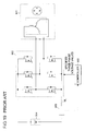
- Fig. 19 is an overall block diagram showing a conventional motor drive system employing the single shunt current detection technique.
- An inverter (PWM inverter) 902 includes three half-bridge circuits provided one for each of three phases and each having an upper arm and a lower arm. The inverter 902 performs individual switching of each arm in accordance with specified three-phase voltage values fed from a controller 903, and thereby converts a direct-current voltage from a direct-current power supply 904 into a three-phase alternating-current voltage. The three-phase alternating-current voltage thus obtained is supplied to a three-phase permanent-magnet synchronous motor 901 to drive and control the motor 901.
- a line connecting each lower arm provided in the inverter 902 with the direct-current power supply 904 is called a bus M L .
- a current sensor 905 transmits, to the controller 903, a signal indicating a bus current flowing through the bus M L .
- the controller 903 performs sampling of an output signal of the current sensor 905 with appropriate timing, and thereby detects a phase current of a phase with a maximum voltage level (maximum phase) and a phase current of a phase with a minimum voltage level (minimum phase), namely, two phase currents.
- Fig. 20 shows an example of how to correct a specified voltage value (pulse width) in general.
- the horizontal axis represents time
- reference characters 920u, 920v, and 920w represent the voltage levels of the U-phase, the V-phase, and the W-phase, respectively. Since the voltage level of each phase is commensurate with the specified voltage value (pulse width) for each phase, they can be considered equivalent. As shown in Fig.
- the specified voltage value (pulse width) of each phase is corrected in such a way that a difference between the voltage levels of the "maximum phase and intermediate phase” and a difference between the voltage levels of the "minimum phase and intermediate phase” do not become equal to or smaller than a predetermined value.
- this correction it becomes possible to detect two phase currents with stability.
- the specified voltage value (pulse width) being corrected, as shown in Fig. 20 , distortion of the phase voltage occurs, leading to an undesirable increase in noise and vibration.
- a motor control device is provided with: a motor current detecting portion for detecting, based on a current flowing between an inverter that drives a three-phase motor and a direct-current power supply, a motor current flowing through the motor; a specified voltage value producing portion for producing, based on the motor current, a specified voltage value as a target value for a voltage to be applied to the motor, and outputting the specified voltage value thus produced; a specified voltage value holding portion for holding an earlier specified voltage value outputted from the specified voltage value producing portion; and a specific period setting portion for setting a specific period based on a voltage difference between two of U-phase, V-phase, and W-phase voltages of the motor. Outside the specific period, the motor is controlled via the inverter based on the specified voltage value outputted from the specified voltage value producing portion, and, within the specific period, the motor is controlled via the inverter based on the specified voltage value held by the specified voltage value holding portion.
- the specific period setting portion includes, in the specific period, a period during which the voltage difference between two of U-phase, V-phase, and W-phase voltages is equal to or smaller than a predetermined threshold value.
- the inverter is provided with a pair of two switching elements, one pair for each of three phases, the pair of two switching elements being connected in series.
- the inverter drives the motor by performing switching control of each switching element based on the specified voltage value outputted from the specified voltage value producing portion or the specified voltage value held by the specified voltage value holding portion.
- the motor current detecting portion detects the current to be measured by converting an analog signal commensurate with the current to be measured into a digital signal, and detects the motor current based on the current to be measured, and the threshold value is previously set according to the attenuation time required for oscillation of the current to be measured to be attenuated, the oscillation occurring at the time of switching of each switching element.
- the motor current detecting portion detects the current to be measured by converting an analog signal commensurate with the current to be measured into a digital signal, and detects the motor current based on the current to be measured, and the threshold value is previously set according to the time required for the analog signal to be converted into the digital signal.
- the inverter is provided with a pair of two switching elements, one pair for each of three phases, the pair of two switching elements being connected in series.
- the inverter drives the motor by performing switching control of each switching element based on the specified voltage value outputted from the specified voltage value producing portion or the specified voltage value held by the specified voltage value holding portion.
- the threshold value is previously set according to the switching delay time of each switching element.
- the specified voltage value holding portion holds the specified voltage value outputted from the specified voltage value producing portion before the specific period.
- the specified voltage value comprises specified voltage values of two phases in rotating coordinates that rotate as a rotor of the motor rotates.
- the motor control device changes the U-phase, V-phase, and W-phase voltages in the specific period according to a position of a rotor of the motor.
- the motor control device is further provided with: an estimating portion for estimating a position of the rotor of the motor; and a coordinate converting portion for converting the specified voltage values of two phases outputted from the specified voltage value producing portion or the specified voltage values of two phases held by the specified voltage value holding portion into specified three-phase voltage values based on the estimated position of the rotor.
- the motor control device controls the motor according to the specified three-phase voltage values. Outside the specific period, the estimating portion estimates the position of the rotor based on the motor current.
- the estimating portion stops estimating the position of the rotor based on the motor current, and estimates, based on the position of the rotor estimated before the specific period, the position of the rotor in the specific period in accordance with changes in the position of the rotor observed before the specific period or in accordance with rotation speed information of the motor obtained before the specific period.
- the motor control device may be provided with: a position detecting portion for detecting a position of the rotor of the motor by using a position sensor; and a coordinate converting portion for converting the specified voltage values of two phases outputted from the specified voltage value producing portion or the specified voltage values of two phases held by the specified voltage value holding portion into specified three-phase voltage values based on the detected position of the rotor, and control the motor according to the specified three-phase voltage values.
- a motor drive system is provided with: a three-phase motor; an inverter that drives the motor; and the aforementioned motor control device controlling the motor by controlling the inverter.
- Fig. 1 is a diagram showing an outline of the overall configuration of the motor drive system.
- the motor drive system shown in Fig. 1 includes a three-phase permanent-magnet synchronous motor 1 (hereinafter referred to simply as a "motor 1”), a PWM (pulse width modulation) inverter 2 (hereinafter referred to simply as an “inverter 2”), a controller 3 functioning as a motor control device, a direct-current power supply 4, and a current sensor 5.
- the direct-current power supply 4 delivers a direct-current voltage between a positive output terminal 4a and a negative output terminal 4b, with the negative output terminal 4b serving as a lower voltage side.
- the motor 1 includes a rotor 6 on which a permanent magnet is provided, and a stator 7 on which U-phase, V-phase, and W-phase armature windings (stator windings) 7u, 7v, and 7w are provided.
- the armature windings 7u, 7v, and 7w are each connected to a neutral point 14 so as to form a Y-connection.
- the armature windings 7u, 7v, and 7w are connected, at their non-connection nodes facing away from the neutral point 14, to terminals 12u, 12v, and 12w, respectively.
- the inverter 2 includes a half-bridge circuit for the U-phase, a half-bridge circuit for the V-phase, and a half-bridge circuit for the W-phase. These three half-bridge circuits form a switching circuit for driving the motor 1.
- Each half-bridge circuit has a pair of switching elements connected in series. In each half-bridge circuit, the pair of switching elements is connected in series between the positive output terminal 4a and the negative output terminal 4b of the direct-current power supply 4. As a result, the direct-current voltage from the direct-current power supply 4 is applied to each half-bridge circuit.
- the half-bridge circuit for the U-phase is composed of a switching element 8u (hereinafter also referred to as an "upper arm 8u”) on a higher voltage side and a switching element 9u (hereinafter also referred to as a "lower arm 9u”) on a lower voltage side.
- the half-bridge circuit for the V-phase is composed of a switching element 8v (hereinafter also referred to as an "upper arm 8v”) on a higher voltage side and a switching element 9v (hereinafter also referred to as a "lower arm 9v”) on a lower voltage side.
- the half-bridge circuit for the W-phase is composed of a switching element 8w (hereinafter also referred to as an "upper arm 8w") on a higher voltage side and a switching element 9w (hereinafter also referred to as a "lower arm 9w") on a lower voltage side.
- a switching element 8w hereinafter also referred to as an "upper arm 8w”
- a switching element 9w hereinafter also referred to as a "lower arm 9w”
- diodes 10u, 10v, 10w, 11u, 11v, and 11w are respectively connected in parallel in such a way that the forward directions thereof point in the direction from the lower voltage side of the direct-current power supply 4 to the higher voltage side thereof.
- the diodes each function as a free-wheel diode.
- a node at which the upper arm 8u and the lower arm 9u are connected in series, a node at which the upper arm 8v and the lower arm 9v are connected in series, and a node at which the upper arm 8w and the lower arm 9w are connected in series are connected to the terminals 12u, 12v, and 12w, respectively.
- a field-effect transistor is shown as an example of the switching element; however, it is also possible to use an IGBT (insulated-gate bipolar transistor) or the like as a substitute for the field-effect transistor.
- the inverter 2 produces PWM signals (pulse width modulation signals) for different phases based on specified three-phase voltage values fed from the controller 3, and feeds the PWM signals thus produced to the control terminals (base or gate) of switching elements provided in the inverter 2, so as to make the switching elements perform switching operation.
- the specified three-phase voltage values fed to the inverter 2 from the controller 3 include a specified U-phase voltage value v u * , a specified V-phase voltage value v v * , and a specified W-phase voltage value v w * representing the voltage levels (voltage values) of a U-phase voltage v u , a V-phase voltage v v , and a W-phase voltage v w , respectively.
- the inverter 2 controls on/off of each switching element (brings it into/out of conduction).
- the direct-current voltage applied to the inverter 2 by the direct-current power supply 4 is modulated by using PWM (pulse width modulation), for example, by the switching operation of the switching elements provided in the inverter 2, and is converted into a three-phase alternating-current voltage.
- PWM pulse width modulation
- the three-phase alternating-current voltage thus obtained is applied to the motor 1, currents commensurate with the three-phase alternating-current voltage flow through the armature windings (7u, 7v, and 7w), whereby the motor 1 is driven.
- the current sensor 5 detects a current (hereinafter referred to as a "bus current") flowing through the bus M L of the inverter 2. Since the bus current has a direct-current component, it can be considered as an equivalent of a direct current.
- bus current a current flowing through the bus M L of the inverter 2. Since the bus current has a direct-current component, it can be considered as an equivalent of a direct current.
- the lower arms 9u, 9v, and 9w are connected together at the lower voltage sides thereof, and are connected to the negative output terminal 4b of the direct-current power supply 4.
- a conductor to which the lower arms 9u, 9v, and 9w are connected together at the lower voltage sides thereof is the bus M L , and the current sensor 5 is connected in series to the bus M L .
- the current sensor 5 transmits, to the controller 3, a signal indicating a current value of the detected bus current (detected current).
- the controller 3 produces the specified three-phase voltage values by referring to the output signal, for example, of the current sensor 5, and outputs the specified three-phase voltage values thus produced.
- the current sensor 5 is, for example, a shunt resistor or a current transformer.
- the current sensor 5 may be connected to a conductor via which the upper arms 8u, 8v, and 8w are connected at the higher voltage sides thereof to the positive output terminal 4a, instead of connecting to the conductor (bus M L ) via which the lower arms 9u, 9v, and 9w are connected at the lower voltage sides thereof to the negative output terminal 4b.
- the currents flowing through the armature windings 7u, 7v, and 7w shown in Fig. 1 are referred to as a U-phase current, a V-phase current, and a W-phase current, respectively, which are individually (or collectively) referred to as a phase current.
- the following description assumes that the polarity of a phase current flowing into the neutral point 14 from the terminals 12u, 12v, or 12w is positive, and the polarity of a phase current flowing from the neutral point 14 is negative.
- Fig. 2 is a diagram showing a typical example of the three-phase alternating-current voltage applied to the motor 1.
- reference characters 100u, 100v, and 100w represent the waveforms of the U-phase voltage, the V-phase voltage, and W-phase voltage, respectively, to be applied to the motor 1.
- the U-phase voltage, the V-phase voltage, and the W-phase voltage are individually (or collectively) referred to as a phase voltage. If a sinusoidal current is passed through the motor 1, the inverter 2 outputs a voltage having a sinusoidal waveform.
- Fig. 2 which of the U-phase voltage, the V-phase voltage, and the W-phase voltage is at the highest, intermediate, and lowest level varies with time. Which of the three voltages is at the highest, intermediate, and lowest level depends on the specified three-phase voltage values, and the inverter 2 determines an energizing pattern of different phases according to the specified three-phase voltage values.
- This energizing pattern is shown in Fig. 3 as a table.
- Fig. 3 shows, from the left, different energizing patterns in the first to third columns; the fourth column will be described later.
- the energizing patterns are an energizing pattern "LLL” in which all the lower arms of the U-, V-, and W-phases are on; an energizing pattern “LLH” in which the upper arm of the W-phase is on, and the lower arms of the U- and V-phases are on; an energizing pattern “LHL” in which the upper arm of the V-phase is on, and the lower arms of the U- and W-phases are on; an energizing pattern "LHH” in which the upper arms of the V- and W-phases are on, and the lower arm of the U-phase is on; an energizing pattern "HLL” in which the upper arm of the U-phase is on, and the lower arms of the V- and W-phases are on; an energizing pattern "HLH” in which the upper arms of the U- and W-phases are on, and the lower arm of the V-phase is on; an energizing pattern "HLH” in which
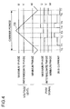
- Fig. 4 shows a relationship between voltage levels of different phase voltages and carrier signal in a case where three-phase modulation is performed, and the corresponding waveforms of the PWM signals and the bus current. Since which of the phase voltages is at the highest, intermediate, and lowest level varies, Fig. 4 deals with a time point 101 shown in Fig. 2 for the sake of concreteness. That is, Fig. 4 shows a state in which the U-phase voltage is at the highest level, and the W-phase voltage is at the lowest level.
- a phase whose voltage level is the highest is referred to as a "maximum phase”
- a phase whose voltage level is the lowest is referred to as a “minimum phase”
- a phase whose voltage level is neither the highest nor the lowest is referred to as an "intermediate phase”.
- the maximum phase, the intermediate phase, and the minimum phase are the U-phase, the V-phase, and the W-phase, respectively.
- reference character CS represents a carrier signal to be compared with the voltage level of each phase voltage.
- the carrier signal is a periodic triangular wave signal, and the period of this signal is called a carrier period.
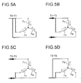
- FIGs. 5A to 5D are each an equivalent circuit diagram of a part around the armature winding, each showing a state in a given period of time shown in Fig. 4 .
- a time point at which a carrier period starts that is, a time point at which the carrier signal is at the lowest level, is referred to as T0.
- T0 a time point at which the carrier signal is at the lowest level.
- the upper arms (8u, 8v, and 8w) of all the phases are turned on. In this case, since no current flows through the direct-current power supply 4 due to formation of a short circuit, as shown in Fig. 5A , the bus current is zero.
- the inverter 2 compares the voltage level of each phase voltage with the carrier signal by referring to v u * , v v * , and v w * .
- the level (voltage level) of the carrier signal starts to increase, and, when the voltage level of the minimum phase crosses the carrier signal at time point T1, the lower arm of the minimum phase is turned on.
- the current of the minimum phase flows as the bus current.
- the W-phase current (with negative polarity) flows as the bus current.
- the level of the carrier signal further increases, and, when the voltage level of the intermediate phase crosses the carrier signal at time point T2, the upper arm of the maximum phase is turned on, and the lower arms of the intermediate phase and the minimum phase are turned on.
- the current of the maximum phase flows as the bus current.
- the U-phase current (with positive polarity) flows as the bus current.
- the level of the carrier signal further increases, and, when the voltage level of the maximum phase crosses the carrier signal at time point T3, the lower arms of all the phases are turned on.
- the bus current is zero.
- the level of the carrier signal starts to decrease.
- the states shown in Figs. 5D, 5C, 5B, and 5A appear in this order. That is, when the level of the carrier signal decreases, let time point at which the voltage level of the maximum phase crosses the carrier signal, time point at which the voltage level of the intermediate phase crosses the carrier signal, time point at which the voltage level of the minimum phase crosses the carrier signal, and time point at which the next carrier period starts be referred to as T4, T5, T6, and T7.
- the energizing patterns between time points T4 and T5, between time points T5 and T6, and between time points T6 and T7 are the same as those between time points T2 and T3, between time points T1 and T2, and between time points T0 and T1, respectively.
- the bus current between time points T1 and T2 or between time points T5 and T6 it is possible to detect the current of the minimum phase based on the bus current thus detected; by detecting the bus current between time points T2 and T3 or between time points T4 and T5, it is possible to detect the current of the maximum phase based on the bus current thus detected.
- the current of the intermediate phase it can be obtained by calculation by exploiting the fact that the total sum of the three-phase currents becomes zero.
- the phase of a current flowing as the bus current in each energizing pattern is shown with the polarity of the current. For example, in the energizing pattern "HHL" given in the eighth row of the table of Fig. 3 , the W-phase current (with negative polarity) flows as the bus current.
- a time period other than a time period between time points T1 and T6 represents the pulse width of the PWM signal for the minimum phase
- a time period other than a time period between time points T2 and T5 represents the pulse width of the PWM signal for the intermediate phase
- a time period other than a time period between time points T3 and T4 represents the pulse width of the PWM signal for the maximum phase.
- a state in which v u > v v > v w holds is referred to as a first mode; a state in which v v > v u > v w holds is referred to as a second mode; a state in which v v > v w > v u holds is referred to as a third mode; a state in which v w > v v > v u holds is referred to as a fourth mode; a state in which v w > v u > v v holds is referred to as a fifth mode; and a state in which v u > v w > v v holds is referred to as a sixth mode.
- the example shown in Figs. 4 and 5A to 5D corresponds to the first mode.
- Fig. 6 also shows the phase of a current detected in each mode.
- the U-phase specified voltage value v u * , the V-phase specified voltage value v v * , and the W-phase specified voltage value v w * are expressed as counter set values CntU, CntV, and CntW, respectively.
- a counter (unillustrated) provided in the controller 3 counts up, starting from 0, from time point T0 every carrier period.
- CntW switching is performed from a state in which the upper arm 8w of the W-phase is on to a state in which the lower arm 9w thereof is on.
- CntV switching is performed from a state in which the upper arm 8v of the V-phase is on to a state in which the lower arm 9v thereof is on.
- CntU switching is performed from a state in which the upper arm 8u of the U-phase is on to a state in which the lower arm 9u thereof is on.
- the carrier signal reaches its maximum level, the count is counted down, and switching operation is performed the other way around.
- a time point at which the count reaches CntW corresponds to time point T1; a time point at which the count reaches CntV corresponds to time point T2; and a time point at which the count reaches CntU corresponds to time point T3.
- a time point at which the count reaches CntW corresponds to time point T1; a time point at which the count reaches CntU corresponds to time point T2; and a time point at which the count reaches CntV corresponds to time point T3.
- the second mode while the count is being counted up, it is possible to detect the W-phase current (with negative polarity) as the bus current flowing at a time point at which the count is greater than CntW and smaller than CntU, and it is possible to detect the V-phase current (with positive polarity) as the bus current flowing at a time point at which the count is greater than CntU and smaller than CntV.
- W-phase current with negative polarity
- V-phase current with positive polarity
- a time point (sampling time point; for example, a time point midway between time points T1 and T2) at which sampling is performed for detecting the phase current of the minimum phase between time points T1 and T2 is represented by reference character ST1
- a time point (sampling time point; for example, a time point midway between time points T2 and T3) at which sampling is performed for detecting the phase current of the maximum phase between time points T2 and T3 is represented by reference character ST2.
- the pulse width (and duty ratio) of the PWM signal for each phase is determined based on the counter set values CntU, CnuV, and CntW given as the specified three-phase voltage values (v u * , v v * , and v w * ).
- phase currents can be detected based on the bus current. It is to be understood, however, that the current waveform of an actual bus current represented by reference character 102 shown in Fig. 7 includes ringing. In addition, there is, for example, a sampling time delay associated with A/D conversion performed on the analog output signal of the current sensor 5. With consideration given to these factors, if a voltage difference between any two of the three phase voltages is equal to or smaller than a predetermined lower limit threshold value V LIM , the actual measurement of two phase currents is impossible.
- a voltage difference between any two of the three phase voltages is referred to as a "voltage difference between two phases”
- a time period during which the actual measurement of two phase currents is impossible is referred to as an "unmeasurable time period”.
- the "voltage difference between two phases” denotes the smallest voltage difference of three voltage differences: a voltage difference between the U-phase voltage and the V-phase voltage, a voltage difference between the V-phase voltage and the W-phase voltage, and a voltage difference between the W-phase voltage and the U-phase voltage.
- T min T d + T rig + T smpl + T power_on - T power_off
- T d represents the previously set dead time
- T rig represents the time that elapsed before the disappearance of ringing in the bus current
- T smpl represents a sampling time delay associated with A/D conversion performed on the analog output signal of the current sensor 5
- T power_off represents the turn-off delay time of the upper or lower arm
- T power_on represents the turn-on delay time of the upper or lower arm.
- the time T min is previously set at the design stage of the motor drive system.
- T rig A further description is given of T rig and the like.
- the inverter 2 performs switching on/off of the upper and lower arms of three phases, and thereby supplies a motor current to the motor 1 to drive it.
- a high-frequency oscillation appears in the current waveform of the bus current.
- This oscillation is generally called ringing.
- This oscillation in the current waveform is attenuated over time, and the time (attenuation time) required for sufficient attenuation of oscillation to achieve a stabilized current waveform of the bus current corresponds to the time T rig .
- the time T rig is previously set at the design stage of the motor drive system by the actual measurement of the current waveform, for example.
- the controller 3 includes an A/D converter (unillustrated) that converts the analog output signal of the current sensor 5 into a digital signal, and detects the current value of the bus current based on the digital signal.
- This A/D converter is provided, for example, in a motor current reconstructing portion 21 (see Fig. 9 ), which will be described later.
- the length of this certain prescribed period corresponds to T smpl .
- the length of this certain prescribed period (that is, time T smpl ) is a unique time length determined by electrical characteristics of the A/D converter, and is previously set at the design stage of the motor drive system.
- the switching elements (8u, 8v, 8w, 9u, 9v, and 9w) are each a field-effect transistor (FET). While an FET is in an on state, suppose that an OFF signal for turning off the FET is fed to the gate of the FET. Then, the FET is completely off when the turn-off delay time has elapsed after the OFF signal was fed to the gate; the FET is in an on state or in the transition state from an on state to an off state until the turn-off delay time has elapsed.
- FET field-effect transistor
- an FET While an FET is in an off state, suppose that an ON signal for turning on the FET is fed to the gate of the FET. Then, the FET is completely on when the turn-on delay time has elapsed after the ON signal was fed to the gate; the FET is in an off state or in the transition state from an off state to an on state until the turn-on delay time has elapsed.
- the turn-off delay time T power_off and the turn-on delay time T power_on are determined by electrical characteristics of each switching element (such as 8u), and are taken into consideration in setting the time T min .
- the turn-off delay time and the turn-on delay time can be collectively called a switching delay time.
- the time T min is uniquely determined by determining T d , T rig , T smpl , T power_off , and T power_on at the design stage of the motor drive system. Based on the time T min and the carrier frequency (the frequency of the carrier signal) adopted by the inverter 2, the smallest voltage difference between two phases, which is necessary for the actual measurement of two phase currents, is uniquely determined. The smallest voltage difference thus determined is equal to the lower limit threshold value V LIM .
- the lower limit threshold value V LIM too is previously determined at the design stage of the motor drive system (controller 3), and is used for determining whether or not the present time is within the unmeasurable time period (or a holding period, which will be described later).
- the motor drive system has the function of maintaining, in the unmeasurable time period, a specified voltage value in rotating coordinates at a specified voltage value obtained before the unmeasurable time period.
- Fig. 8 is an analysis model diagram of the motor 1.
- Fig. 8 shows the U-phase, V-phase, and W-phase armature winding fixed axes (hereinafter also referred to simply as the "U-phase axis", the "V-phase axis”, and the "W-phase axis").
- Reference character 6a represents the permanent magnet provided on the rotor 6 of the motor 1.
- the direction of the magnetic flux produced by the permanent magnet 6a is referred to as the d-axis
- the rotation axis for control purposes, the rotation axis corresponding to the d-axis is referred to as the ⁇ -axis.
- the axis having a phase leading the d-axis by an electrical angle of 90 degrees is referred to as the q-axis
- the axis having a phase leading the ⁇ -axis by an electrical angle of 90 degrees is referred to as the ⁇ -axis.
- the d-axis and the q-axis are collectively referred to as the d-q axes, and the coordinates having the d-q axes as their coordinate axes are referred to as the d-q coordinates.
- the ⁇ -axis and the ⁇ -axis are collectively referred to as the ⁇ - ⁇ axes, and the coordinates having the ⁇ - ⁇ axes as their coordinate axes are referred to as the ⁇ - ⁇ coordinates.
- the d-q axes rotates, and its rotation speed is represented by ⁇ .
- the ⁇ - ⁇ axes also rotates, and its rotation speed is represented by ⁇ e .
- the phase (angle) of the d-axis at a given moment is represented, relative to the U-phase armature winding fixed axis, by ⁇ .
- the phase (angle) of the ⁇ -axis at that given moment is represented, relative to the U-phase armature winding fixed axis, by ⁇ e .
- ⁇ ⁇ - ⁇ e .
- the phase (angle) represented by ⁇ or ⁇ e is the phase (angle) in electrical angle, and is referred to as a rotor position, as commonly called.
- the rotation speed represented by ⁇ or ⁇ e is the angular velocity at electrical angle.
- the whole of the motor voltage applied to the motor 1 from the inverter 2 is referred to as the motor voltage V a
- the whole of the motor current supplied to the motor 1 from the inverter 2 is referred to as the motor current I a .
- the ⁇ -axis component, the ⁇ -axis component, the d-axis component, and the q-axis component of the motor voltage V a are referred to as the ⁇ -axis voltage v ⁇ , the ⁇ -axis voltage v ⁇ , the d-axis voltage v d , and the q-axis voltage v q , respectively.
- the ⁇ -axis component and the ⁇ -axis component of the motor current I a are referred to as the ⁇ -axis current i ⁇ and the ⁇ -axis current is, respectively.
- the value specifying the ⁇ -axis voltage v ⁇ and the value specifying the ⁇ -axis voltage v ⁇ are referred to as the specified ⁇ -axis voltage value v ⁇ * and the specified ⁇ -axis voltage value v ⁇ * , respectively.
- the specified ⁇ -axis voltage value v ⁇ * represents the voltage (voltage value) to be followed by v ⁇
- the specified ⁇ -axis voltage value v ⁇ * represents the voltage (voltage value) to be followed by v ⁇ .
- the value specifying the ⁇ -axis current i ⁇ and the value specifying the ⁇ -axis current is are referred to as the specified ⁇ -axis current value i ⁇ * and the specified ⁇ -axis current value i ⁇ * , respectively.
- the specified ⁇ -axis current value i ⁇ * represents the current (current value) to be followed by i ⁇
- the specified ⁇ -axis current value i ⁇ * represents the current (current value) to be followed by i ⁇ .
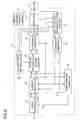
- FIG. 9 is a detailed block diagram of the motor drive system according to Example 1.
- the controller 3 includes different parts represented by reference numerals 21 to 28.
- the different parts constituting the motor drive system can freely use all the values produced within the motor drive system as necessary.
- the motor current reconstructing portion 21 reconstructs the motor current I a by specifying, based on the specified three-phase voltage values (v u * , v v * , and v w * ) outputted from the coordinate converter 27, the sampling time point ST1 at which the phase current of the minimum phase is detected and the sampling time point ST2 at which the phase current of the maximum phase is detected (see Fig. 6 ), then sampling the analog output signal from the current sensor 5 at the sampling time points ST1 and ST2, and then performing A/D conversion on the sampled analog output signals. Specifically, the motor current reconstructing portion 21 reconstructs the U-phase current i u and the V-phase current i v , and sends them to the coordinate converter 22.
- the motor current reconstructing portion 21 exploits, if necessary, the fact that the total sum of the U-phase current i u , the V-phase current i v , and the W-phase current i w is zero. It is to be understood that, as far as the current is concerned, to "reconstruct the current” is synonymous with to "detect the current”. Therefore, the motor current reconstructing portion can be also called the motor current detecting portion.
- the coordinate converter 22 calculates the ⁇ -axis current i ⁇ and the ⁇ -axis current is, and outputs them.
- the speed controller 23 calculates the specified ⁇ -axis current value i ⁇ * and the specified ⁇ -axis current value i ⁇ * such that the speed error ( ⁇ * - ⁇ e ) is made to converge to zero, and outputs them.
- the current controller 24 calculates the specified ⁇ -axis voltage value v ⁇ * and the specified ⁇ -axis voltage value v ⁇ * such that the current errors (i ⁇ * - i ⁇ ) and (i ⁇ * - is) are made to converge to zero, and outputs them.
- the different parts constituting the controller 3 update, at intervals of a predetermined period, the specified values (including i ⁇ i ⁇ * , v ⁇ * , v ⁇ * , v u * , v v * , and v w * ) or the state quantities (including i u , i v , i ⁇ , is, ⁇ e , and ⁇ e ) calculated thereby and outputted therefrom.
- the holding period setting portion 25 determines whether or not the voltage difference between two phases is equal to or smaller than the lower limit threshold value V LIM based on the specified three-phase voltage values (v u * , v v * , and v w * ) outputted from the coordinate converter 27, and sets a holding period based on the determination results.
- the holding period setting portion 25 sets the holding period such that it fully covers the period (that is, the unmeasurable time period) during which the voltage difference between two phases is equal to or smaller than the lower limit threshold value V LIM .
- the holding period is so set as to coincide with the period during which the voltage difference between two phases is equal to or smaller than the lower limit threshold value V LIM .
- the specified voltage value holding portion 26 holds v ⁇ * and v ⁇ * outputted from the current controller 24 at a particular time point under the control of the holding period setting portion 25. Outside the holding period, the specified voltage value holding portion 26 outputs v ⁇ * and v ⁇ * the current controller 24 is outputting, as they are, to the coordinate converter 27. Within the holding period, the specified voltage value holding portion 26 outputs V ⁇ * and v ⁇ * held thereby to the coordinate converter 27. It is to be noted that, even outside the holding period, the specified voltage value holding portion 26 may hold v ⁇ * and v ⁇ * outputted at a particular time point (these values are not fed to the coordinate converter 27).
- the holding period is related to a period during which the specified voltage value holding portion 26 holds v ⁇ * and v ⁇ * outputted at a particular time point, they do not always completely correspond with each other (they, however, sometimes correspond with each other).
- the "holding period” described in this embodiment can be replaced by the "specific period”.
- the coordinate converter 27 calculates the specified three-phase voltage values (v u * , v, * , and v w * ) by performing coordinate conversion, based on the rotor position ⁇ e outputted from the estimator 28, so that v ⁇ * and v ⁇ * fed from the specified voltage value holding portion 26 are converted into those on the three-phase fixed coordinate axes, and outputs them.
- the estimator 28 estimates the rotor position ⁇ e and the rotation speed ⁇ e such that the axis error ⁇ (see Fig. 8 ) between the d- and ⁇ -axes is made to converge to zero by performing, for example, proportional-plus-integral control by using all or part of i ⁇ and is outputted from the coordinate converter 22 and v ⁇ * and v ⁇ * outputted from the current controller 24.
- various methods for estimating the rotor position ⁇ e and the rotation speed ⁇ e can be adopted in the estimator 28. For example, a method that is disclosed in JP-B-3411878 may be adopted.
- the rotor position ⁇ e estimated by the estimator 28 is outputted to the coordinate converters 22 and 27, and the rotation speed ⁇ e estimated by the estimator 28 is outputted to the speed controller 23.
- the inverter 2 controls the switching of each arm provided in the inverter 2 in accordance with the specified three-phase voltage values outputted from the coordinate converter 27, and thereby supplies the motor current I a commensurate with the specified values (such as i ⁇ * and i ⁇ * ) produced in the controller 3 to the motor 1 to drive it.
- Fig. 10 shows a schematic operating procedure of the controller 3, with attention focused on the voltage difference between two phases.
- the controller 3 sets a period during which the voltage difference between two phases is relatively small as the holding period, and performs, for example, position sensorless vector control in the holding period by using v ⁇ * and v ⁇ * obtained immediately before the holding period.
- the controller 3 calculates V ⁇ * . and v ⁇ * based on the detected i u and i v , and performs position sensorless vector control based on v ⁇ * and v ⁇ * thus calculated.
- FIG. 11 illustrates how v ⁇ * , v ⁇ * , ⁇ e , ⁇ e , i u , i v , i ⁇ , and is change, with the horizontal axis representing time, showing the transition from a state in which the U-phase voltage is the maximum phase and the V-phase voltage is the intermediate phase to a state in which the U-phase voltage is the intermediate phase and the V-phase voltage is the maximum phase.
- v ⁇ * , v ⁇ * , ⁇ e , ⁇ e , i u , i v , i ⁇ and is are discrete values that are updated at intervals of a predetermined period.
- v ⁇ * , v ⁇ * , ⁇ e , ⁇ e , i u , i v , i ⁇ and is at an update time point t are represented by v ⁇ * [t], v ⁇ * [t], ⁇ e [t], ⁇ e [t], i u [t], i v [t], i ⁇ [t], and i ⁇ [t], respectively.
- ⁇ * , i ⁇ * , i ⁇ * , v u * , v v * , and v w * at the update time point t are represented by ⁇ * [t], i ⁇ * [t], i ⁇ * [t], v u * [t], v v * [t], and v w * [t], respectively.
- the update time point does not mean an instantaneous time point, but does mean a time concept having a given width with consideration given to operation time or the like.
- the length of a period between the update time point t and the next update time point (t + 1) corresponds to the aforementioned predetermined period.
- i u [t], i v [t], and ⁇ e [t-1] i ⁇ [t] and i ⁇ [t] are calculated; based on i ⁇ [t], i ⁇ [t], v ⁇ * [t -1], and v ⁇ * [t -1], ⁇ e [t] and ⁇ e [t] are calculated; and, based on ⁇ * [t] and ⁇ e [t], i ⁇ * [t] and i ⁇ * [t] are calculated.
- the current controller 24 calculates v ⁇ * [t] and v ⁇ * [t] based on i ⁇ * [t], i ⁇ * [t], i ⁇ [t], and i ⁇ [t].
- the coordinate converter 27 calculates v * u [t], v v * [t], and v w * [t] based on ⁇ e [t] and v ⁇ * [t] and v ⁇ * [t] fed thereto.
- the holding period setting portion 25 determines that a period from an update time point (t + 1) onward is included in the particular holding period based on v u * [t], v v * [t], and v w * [t] and that the particular holding period ends at an update time point (t + k). That is, a period from the update time point (t + 1) to the update time point (t + k) is included in one holding period, and a period from the update time point (t + k + 1) onward is not included in this holding period.
- k is an integer equal to or greater than 2.
- i u [t] and i v [t] are calculated by the actual measurement using the current sensor 5, i ⁇ [t] and i ⁇ [t] are calculated, and ⁇ e [t] and ⁇ e [t] are then calculated.
- i ⁇ * [t] and i ⁇ * [t] are calculated by the speed controller 23
- v ⁇ * [t] and v ⁇ * [t] calculated by the current controller 24 are fed, as they are, to the coordinate converter 27 via the specified voltage value holding portion 26.
- the coordinate converter 27 calculates v u * [t], v v *[t], and v w * [t].
- the output signal of the current sensor 5 is not sampled, and i u , i v , i ⁇ , and is are not calculated. It is to be noted that, even in the holding period, the output signal of the current sensor 5 may be sampled (without calculating values such as i u according to the sampled value thus obtained).
- the estimator 28 temporarily stops estimating ⁇ e and ⁇ e based on i ⁇ and i ⁇ . Instead, the estimator 28 estimates ⁇ e in the holding period such that ⁇ e is made to change in accordance with changes in ⁇ e observed on or before the update time point t or in accordance with the rotation speed information obtained on or before the update time point t.
- the rotation speed information obtained on or before the update time point t includes ⁇ e [t] or ⁇ *[t]. In a steady state, ⁇ e [t] is almost the same as ⁇ * [t].
- ⁇ e in the holding period (that is, ⁇ e [t+ 1] to ⁇ e [t + k]) is estimated based on ⁇ e [t] on the presumption that the rotor 6 keeps rotating at a rotation speed of ⁇ e [t] or ⁇ * [t] in the holding period. Therefore, ⁇ e in the holding period (that is, ⁇ e [t + 1] to ⁇ e [t + k]) is regarded as the same as ⁇ e [t].
- the rotor position and rotation speed (such as ⁇ e [t + 1] and ⁇ e [t + 1]) estimated in the holding period are outputted to the coordinate converter 27 and the speed controller 23. Since the rotor keeps rotating at a constant rate in a steady state, estimating ⁇ e and ⁇ e in the holding period in the above-described manner presents little problem.
- the specified voltage value holding portion 26 holds v ⁇ * and v ⁇ * outputted from the current controller 24 immediately before the holding period. That is, the specified voltage value holding portion 26 holds v ⁇ * [t] and v ⁇ * [t], and continuously outputs them in the holding period.
- v ⁇ * and v ⁇ * (that is, v ⁇ * [t + 1] to v ⁇ * [t + k] and v ⁇ * [t + 1] to v ⁇ * [t + k]) fed to the coordinate converter 27 from the update time point (t + 1) to the update time point (t + k) are the same as v ⁇ * [t] and v ⁇ * [t] outputted from the current controller 24 immediately before the holding period.
- i ⁇ * [t + k + 1] and i ⁇ * [t + k + 1] are calculated by the speed controller 23
- the coordinate converter 27 calculates v u * [t + k + 1], v v * [t + k + 1], and v w * [t+k+1]. The same holds true for a period from an update time point (t + k + 2) onward.
- the voltage waveform observed when the holding operation described above is performed is shown in Fig. 12 .
- the horizontal axis represents time
- reference character 103 represents the voltage waveform of the U-phase voltage v u
- reference character 104 represents the waveform of v ⁇ *
- reference character 105 represents the waveform of v ⁇ * .
- the holding period is located in an area 106 encircled with broken lines and in an area 107 encircled with broken lines.
- the obtained U-phase voltage v u is a smooth, distortion-free voltage. That is, unlike the method for correcting the pulse width (see Fig. 20 ), there is no possibility that voltage distortion (discontinuity in specified voltage) occurs.
- a conventional method described in JP-A-2004-64903 requires a complicated calculation process for re-converting d-q axes currents into three-phase currents in the unmeasurable time period, the d-q axes currents obtained by performing dq conversion on the three-phase currents obtained before the unmeasurable time period. Such a complicated calculation process is not required in this example. Let the symbols used in this embodiment be applied to this conventional method. Then, in this conventional method, a calculation process is required in which the speed controller and the current controller calculate, in the unmeasurable time period, i ⁇ * , i ⁇ * , v ⁇ * , and v ⁇ * based on i ⁇ and i ⁇ obtained before the unmeasurable time period.
- this example eliminates the possibility of occurrence of such a calculation error, making it possible to perform vector control of the motor 1 with a higher degree of accuracy.
- the specified voltage value holding portion 26 holds v ⁇ * and v ⁇ * outputted from the current controller 24 immediately before the holding period, that is, v ⁇ * [t] and v ⁇ * [t], and continuously outputs them in the holding period.
- the specified voltage value held by the specified voltage value holding portion 26 and outputted therefrom in the holding period does not necessarily have to be v ⁇ * [t] and v ⁇ * [t].
- j is an integer equal to or greater than 1, it is preferable that the value of j be as small as possible, because v ⁇ * and v ⁇ * should be calculated based on the values measured by the current sensor 5; most preferably, j is equal to 0, just as described in the example above.
- the specified voltage value holding portion 26 holds v ⁇ * and v ⁇ * outputted from the current controller 24 before a particular holding period, that is, v ⁇ * [t - j] and v ⁇ * [t - j], and continuously outputs them in the particular holding period (here, j is an integer equal to or greater than 0, and is previously set as a fixed value, for example). More specifically, the specified voltage value holding portion 26 holds v ⁇ * [t-j] and v ⁇ * [t-j], the values outputted from the current controller 24 at a particular time point before the holding period, the particular time point determined relative to a time point from which the holding period begins, and continuously outputs them in the holding period.
- v ⁇ * and v ⁇ * fed to the coordinate converter 27 from the update time point (t + 1) to the update time point (t + k) are the same as v ⁇ * [t - j] and v ⁇ * [t - j] outputted from the current controller 24.
- the holding period setting portion 25 sets the holding period will be explained. Examples of such a setting method are first and second setting methods.
- the holding period setting portion 25 can adopt either the first or second setting method.
- the holding period setting portion 25 determines whether or not the voltage difference between two phases is equal to or smaller than the aforementioned lower limit threshold value V LIM based on the specified three-phase voltage values (v u * , v v * , and v w * ) at all times, and includes a period during which the voltage difference between two phases is equal to or smaller than the lower limit threshold value V LIM in the holding period.
- the holding period setting portion 25 determines whether or not the voltage difference between two phases is equal to or smaller than the lower limit threshold value V LIM based on the specified three-phase voltage values (v u * , v v * , and v w * ), and sets a time point (or a time point a little before that time point) at which a transition is made from a state in which the voltage difference between two phases is greater than the lower limit threshold value V LIM to a state in which the voltage difference between two phases is equal to or smaller than the lower limit threshold value V LIM as a start point of the holding period.
- the holding period setting portion 25 sets the length of the holding period based on the rotation speed information ( ⁇ e or ⁇ * ) obtained at the start point of the holding period. This is because, since the rotor keeps rotating at a constant rate in a steady state, it is possible to estimate, based on the rotation speed information, how much time elapses until the voltage difference between two phases becomes greater than the lower limit threshold value V LIM again. Once the start point and length of the holding period are set, the end point of the holding period is automatically determined.
- Example 1 deals with the first and second setting methods as an example of the holding period setting method. Instead, it is also possible to use a third setting method. As an example using the third setting method, Example 2 will be described. Example 2 differs from Example 1 in the holding period setting method. In other respects, Examples 1 and 2 are the same. Therefore, in the following description, explanations will be given with emphasis placed on the holding period setting method of Example 2.
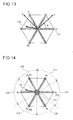
- Fig. 13 is a spatial vector diagram showing a relationship among fixed axes including the U-phase axis, the V-phase axis, and the W-phase axis, rotation axes including the d-axis and the q-axis, and voltage vector.
- a vector represented by reference numeral 110 is the voltage vector.
- the phase of the voltage vector 110 relative to the q-axis is represented by ⁇ .
- the phase of the voltage vector 110 relative to the U-phase axis is represented by ( ⁇ + ⁇ + ⁇ / 2).
- the voltage vector 110 is the voltage that is applied to the motor 1 and viewed as a vector.
- the ⁇ -axis component and the ⁇ -axis component of the voltage vector 110 are v ⁇ and v ⁇ , respectively.
- the specified ⁇ -axis voltage value v ⁇ * and the specified ⁇ -axis voltage value v ⁇ * are calculated, and the voltage vector 110 is represented by using v ⁇ * and v ⁇ * . Therefore, the voltage vector can also be referred to as a specified voltage vector.
- Hatched areas 111 that are shaped like an asterisk and include an area near the U-phase axis, an area near the V-phase axis, and an area near the W-phase axis each represent an area in which two phase currents cannot be detected.
- the voltage vector 110 is located near the U-phase axis; in a case where two phase currents cannot be detected due to closeness of voltage levels of the U-phase voltage and the W-phase voltage, the voltage vector 110 is located near the V-phase axis.
- the areas 111 in which two phase currents cannot be detected are spaced an electrical angle of 60 degrees apart relative to the U-phase axis. If the voltage vector 110 is located in any of the areas 111, two phase currents cannot be detected. Therefore, by determining whether or not the voltage vector (specified voltage vector) at a particular time point is located in any of the areas 111, it is possible to determine whether or not that particular time point should be included in the holding period.
- a-b coordinates Incidentally, the d-q and ⁇ - ⁇ coordinates rotate in a continuous manner.
- the a-b coordinates have, as their coordinate axes, the a- and b-axes at right angles to each other.
- Fig. 14 shows six potential a-axes.
- the a-axis can be any one of a 1 - to a 6 -axes according to the phase ( ⁇ + ⁇ + ⁇ / 2) of the voltage vector 110.
- the a 1 -, a 3 -, and as-axes coincide with the U-, V-, and W-phase axes, respectively.
- the a 2 -, a 4 -, and a 6 -axes correspond to an axis intermediate between the a 1 - and a 3 -axes, an axis intermediate between the a 3 - and a 5 -axes, and an axis intermediate between the a 5 - and a 1 -axes, respectively.
- a circle represented by reference numeral 131 will be described later.
- the a-axis is the a 1 -axis. If the voltage vector 110 is located in a region represented by reference numeral 122, that is, if ⁇ / 6 ⁇ ( ⁇ + ⁇ + ⁇ / 2) ⁇ ⁇ / 2 holds, the a-axis is the a 2 -axis.
- the a-axis is the a 3 -axis. If the voltage vector 110 is located in a region represented by reference numeral 124, that is, if 5 ⁇ / 6 ⁇ ( ⁇ + ⁇ + ⁇ / 2) ⁇ 7 ⁇ / 6 holds, the a-axis is the a 4 -axis.
- the a-axis is the a 5 -axis. If the voltage vector 110 is located in a region represented by reference numeral 126, that is, if 3 ⁇ / 2 ⁇ ( ⁇ + ⁇ + ⁇ /2 ) ⁇ 11 ⁇ /6 holds, the a-axis is the a 6 -axis. For example, in a case where the voltage vector 110 lies in a position shown in Fig. 14 , the a-axis is the a 4 -axis.
- the a-axis rotates every 60 degrees in a step-like manner as the voltage vector rotates
- the b-axis also rotates every 60 degrees along with the a-axis in a step-like manner, forming a right angle with the a-axis.
- the a- and b-axes can be expressed as the coordinate axes that rotate every 60 degrees and that are quantized with a rotation angle of 60 degrees. As a result, the a-axis is always located at the center of the area in which two phase currents cannot be detected.
- the voltage vector 110 is a voltage vector in the a-b coordinates obtained by subjecting the d-q coordinates to coordinate conversion by the phase difference ⁇ D
- the voltage vector 110 in the a-b coordinates has, as its a-axis and b-axis components, the a-axis voltage v a and the b-axis voltage v b .
- the d-axis voltage v d , the q-axis voltage v q , the a-axis voltage v a , and the b-axis voltage v b satisfy the coordinate conversion formula (1-3) below.
- ( v a v b ) cos ⁇ D - sin ⁇ D sin ⁇ D cos ⁇ D ( v d v q )
- phase difference ⁇ D can be calculated as follows.
- n i.e., a quotient obtained by dividing ( ⁇ + ⁇ ) by ⁇ / 3 which matches ⁇ given by formula (1-4) below is obtained.
- n a quotient obtained by dividing ( ⁇ + ⁇ ) by ⁇ / 3
- ⁇ ⁇ / 3
- a determination as to whether or not the voltage vector (specified voltage vector) is located in the areas 111 is made possible by performing coordinate conversion so that the voltage vector in the d-q coordinates is converted into the one in the a-b coordinates, and then referring to the a-axis and b-axis components of the voltage vector in the a-b coordinates.
- the voltage vector 110 lies within the circle 131, the voltage levels of three phase voltages are close to one another. Also in this case, it is impossible to detect two phase currents.
- Fig. 16 is an internal block diagram of a holding period setting portion 25a according to Example 2.
- the holding period setting portion 25a includes a coordinate rotating portion 41 and a judging portion 42.
- v ⁇ * and v ⁇ * outputted from the specified voltage value holding portion 26 and ⁇ e outputted from the estimator 28 are used as v d , v q , and ⁇ , respectively, in formulae such as formulae (1-1) to (1-4) above.
- the coordinate rotating portion 41 performs coordinate conversion according to formula (1-3) above on v ⁇ * and v ⁇ * outputted from the specified voltage value holding portion 26 by using ⁇ e outputted from the estimator 28, and obtains the a-axis voltage v a and the b-axis voltage v b .
- the aforementioned method using formula (1-4) above is used.
- the judging portion 42 makes a judgment on the voltage difference between two phases. Specifically, the judging portion 42 makes a judgment as to whether or not the magnitude (absolute value) of the b-axis voltage v b is smaller than a predetermined threshold value ⁇ (where ⁇ > 0). That is, the judging portion 42 makes a judgment as to whether or not formula (1-5) below holds (see Fig. 17 for the significance of the threshold value ⁇ ). In addition, the judging portion 42 makes a judgment as to whether or not the a-axis voltage v a satisfies formula (1-6) below.
- the judging portion 42 judges that the voltage difference between two phases is equal to or smaller than the aforementioned lower limit threshold value V LIM ; if neither formula (1-5) nor formula (1-6) holds, the judging portion 42 judges that the voltage difference between two phases is greater than the lower limit threshold value V LIM .
- the holding period setting portion 25a sets the holding period in such a way that the period during which the voltage difference between two phases is equal to or smaller than the lower limit threshold value V LIM is included in the holding period.
- the different parts the specified voltage value holding portion 26, the estimator 28, and the like provided in the motor drive system operate in accordance with the holding period set by the holding period setting portion 25a.
- Example 2 It is needless to say that the same effects as those achieved in Example 1 can be achieved by setting the holding period in the manner described in Example 2.
- Examples 1 and 2 deal with the motor drive systems in which vector control is performed such that the axis error ⁇ between the d- and ⁇ -axes is made to converge to zero, that is, such that the ⁇ -axis is made to follow the d-axis; however, Examples 1 and 2 may be modified to be Example 3 in which vector control is performed such that the ⁇ -axis is made to follow an axis other than the d-axis.
- vector control may be performed such that the ⁇ -axis is made to follow the dm-axis.
- the dm-axis is an axis that lags behind the qm-axis by an electrical angle of 90 degrees.
- the qm-axis is the rotation axis whose direction coincides with that of the current vector to be fed to the motor 1 when maximum torque control is achieved.
- the current vector to be fed to the motor 1 is the current to be fed to the motor 1 and expressed in vector form.
- the qm-axis may be the rotation axis having a phase leading the rotation axis whose direction coincides with that of the current vector to be fed to the motor 1 when maximum torque control is achieved.
- the estimator 28 shown in Fig. 9 estimates the axis error ⁇ m between the dm- and ⁇ -axes by using all or part of i ⁇ and is outputted from the coordinate converter 22 and v ⁇ * and v ⁇ * outputted from the current controller 24, and estimates the rotor position ⁇ e and the rotation speed ⁇ e such that the axis error ⁇ m is made to converge to zero by using proportional-plus-integral control.
- the operation performed in the holding period is the same as those of Examples 1 and 2.
- Examples 1 to 3 deal with the motor drive systems in which position sensorless vector control is performed that uses no position sensor for detecting the rotor position. However, the techniques described in Examples 1 to 3 are useful in a case where the position sensor is provided. As Example 4 of the invention, a description will be given below of a motor drive system provided with the position sensor. Any feature of Examples 1 to 3 can be applied, unless inconsistent, to Example 4.
- Fig. 18 is a block diagram of the motor drive system having this configuration.
- This motor drive system differs from the motor drive system shown in Fig. 9 in that ⁇ e and ⁇ e are detected based on the output signal of the position sensor, and that this eliminates the need for the estimator 28. In other respects, this motor drive system is the same as that shown in Fig. 9 .
- the position sensor 51 is realized with, for example, Hall devices or resolvers, and outputs a signal for specifying the magnetic pole position of the permanent magnet 6a of the rotor 6 (that is, a signal for specifying the angle ⁇ ).
- the position detecting portion 52 detects the phase of the d-axis, relative to the U-phase armature winding fixed axis, based on the output signal of the position sensor 51.
- the phase (rotor position) thus detected is treated as ⁇ e .
- the rotor position ⁇ e detected by the position detecting portion 52 is, ideally, equal to ⁇ shown in Fig. 8 , and is fed to the coordinate converters 22 and 27.
- the rotor position ⁇ e is differentiated by the differentiator 53 to obtain ⁇ e , and ⁇ e thus obtained is fed to the speed controller 23.
- the specified voltage value holding portion 26 holds v ⁇ * and v ⁇ * outputted from the current controller 24 at a particular time point. Outside the holding period, the specified voltage value holding portion 26 outputs v ⁇ * and v ⁇ * the current controller 24 is outputting, as they are, to the coordinate converter 27. Within the holding period, the specified voltage value holding portion 26 outputs v ⁇ * and v ⁇ * held thereby to the coordinate converter 27. As a result of the position sensor 51 being used, the rotor position ⁇ e is always detected irrespective of whether or not the present time is within the holding period.
- the coordinate converter 27 performs, based on the rotor position ⁇ e detected based on the output signal of the position sensor 51 at all times, coordinate conversion so that v ⁇ * and v ⁇ * fed from the specified voltage value holding portion 26 are converted into those on the three-phase fixed coordinate axes, and thereby calculates the specified three-phase voltage values (v u * , v v * , and v w * ) and outputs them.
- Example 4 It is needless to say that the same effects (such as obtaining a smooth voltage waveform of the phase voltage) as those achieved in Example 1 can be achieved by configuring the motor drive system as in Example 4.
- notes 1 to 4 will be described as modified examples of the embodiment described above or annotations made thereon. Any feature of notes 1 to 4 described below can be applied, unless inconsistent, to any note other than that in connection with which the feature is specifically described.
- the modulation method used in the present invention is not limited to three phase modulation.
- the energizing patterns are different from those of three-phase modulation shown in Fig. 3 .
- the lower arm of the minimum phase since the lower arm of the minimum phase is always on, there are no energizing patterns corresponding to the energizing patterns between time points T0 and T1 and between time points T6 and T7 shown in Fig. 4 .
- Part or all of the functions of the controller 3 shown in Fig. 1 is realized, for example, with software (program) incorporated in a general-purpose microcomputer or the like.
- software program
- the block diagrams showing the configurations of different parts of the controller 3 serve as functional block diagrams.
- the controller 3 may be realized with hardware alone, instead of software (program), or may be realized with a combination of software and hardware.
- the present invention is suitable for electric devices of any kind that use a motor; for example, it is suitable for electric cars that run by exploiting the rotation of a motor, compressors for use in refrigerators, and air-conditioning apparatuses (in particular, for example, in-vehicle air-conditioning apparatuses).
Abstract
Description
- The present invention relates to motor control devices that drive and control a motor, and more particularly to a motor control device employing a single shunt current detection technique.
- In order to perform vector control of a motor by supplying three-phase alternating-current power to the motor, it is necessary to detect two phase currents (for example, a U-phase current and a V-phase current) among three phase currents consisting of U-phase, V-phase, and W-phase currents. In general, detection of two phase currents is performed by using two current sensors (such as current transformers). However, the use of two current sensors undesirably increases overall cost of a system incorporating the motor.
- It is for this reason that there has conventionally been proposed a technique by which a bus current (direct current) between an inverter and a direct-current power supply is detected with a single current sensor, and, based on the bus current thus detected, two phase currents are detected. This technique is called a single shunt current detection technique, and the basic principle of this technique is described, for example, in
JP-B-2712470 -
Fig. 19 is an overall block diagram showing a conventional motor drive system employing the single shunt current detection technique. An inverter (PWM inverter) 902 includes three half-bridge circuits provided one for each of three phases and each having an upper arm and a lower arm. Theinverter 902 performs individual switching of each arm in accordance with specified three-phase voltage values fed from acontroller 903, and thereby converts a direct-current voltage from a direct-current power supply 904 into a three-phase alternating-current voltage. The three-phase alternating-current voltage thus obtained is supplied to a three-phase permanent-magnetsynchronous motor 901 to drive and control themotor 901. - A line connecting each lower arm provided in the
inverter 902 with the direct-current power supply 904 is called a bus ML. Acurrent sensor 905 transmits, to thecontroller 903, a signal indicating a bus current flowing through the bus ML. Thecontroller 903 performs sampling of an output signal of thecurrent sensor 905 with appropriate timing, and thereby detects a phase current of a phase with a maximum voltage level (maximum phase) and a phase current of a phase with a minimum voltage level (minimum phase), namely, two phase currents. - If there is a sufficient level difference among the voltage levels of different phases, two phase currents can be detected in the above-described manner. However, if the voltage levels of the maximum phase and intermediate phase come close to each other, or the voltage levels of the minimum phase and intermediate phase come close to each other, it becomes impossible to detect two phase currents. Incidentally, the single shunt current detection technique will be described later with reference to
Fig. 3 to Figs. 5A to 5D , along with the reason why it becomes impossible to detect two phase currents. - In view of this, there has been proposed a technique of correcting the pulse width of a PWM signal for each arm provided in the inverter based on the three-phase gate signals in the time period during which two phase currents cannot be detected by the single shunt current detection technique (see, for example,
JP-A-2003-189670 - As an example of such a correction technique,
Fig. 20 shows an example of how to correct a specified voltage value (pulse width) in general. InFig. 20 , the horizontal axis represents time, andreference characters Fig. 20 , the specified voltage value (pulse width) of each phase is corrected in such a way that a difference between the voltage levels of the "maximum phase and intermediate phase" and a difference between the voltage levels of the "minimum phase and intermediate phase" do not become equal to or smaller than a predetermined value. With this correction, it becomes possible to detect two phase currents with stability. However, as a result of the specified voltage value (pulse width) being corrected, as shown inFig. 20 , distortion of the phase voltage occurs, leading to an undesirable increase in noise and vibration. - It is for this reason that a technique of handling the time period during which two phase currents cannot be detected without correcting the specified voltage value (pulse width) is sought after.
- For example, there has been proposed a method for estimating three-phase currents by re-converting d-q axes currents into three-phase currents in the time period during which two phase currents cannot be detected, the d-q axes currents obtained by performing dq conversion on the three-phase currents obtained before that time period (see, for example,
JP-A-2004-64903 - There has also been proposed a method for allowing the carrier frequency of the PWM inverter to be changed, and reducing the carrier frequency as necessary for making it possible to detect two phase currents (see, for example,
JP-A-2005-45848 JP-A-2003-224982 JP-A-2004-104977 - It is an object of the present invention to provide motor control devices and motor drive systems that employ a single shunt current detection technique and that can deal with, by simple processing, a period during which the actual measurement of a phase current is impossible.
- According to one aspect of the present invention, a motor control device is provided with: a motor current detecting portion for detecting, based on a current flowing between an inverter that drives a three-phase motor and a direct-current power supply, a motor current flowing through the motor; a specified voltage value producing portion for producing, based on the motor current, a specified voltage value as a target value for a voltage to be applied to the motor, and outputting the specified voltage value thus produced; a specified voltage value holding portion for holding an earlier specified voltage value outputted from the specified voltage value producing portion; and a specific period setting portion for setting a specific period based on a voltage difference between two of U-phase, V-phase, and W-phase voltages of the motor. Outside the specific period, the motor is controlled via the inverter based on the specified voltage value outputted from the specified voltage value producing portion, and, within the specific period, the motor is controlled via the inverter based on the specified voltage value held by the specified voltage value holding portion.
- This makes it possible to deal with, by simply holding the specified voltage value, a period during which the actual measurement of a phase current is impossible.
- Specifically, for example, the specific period setting portion includes, in the specific period, a period during which the voltage difference between two of U-phase, V-phase, and W-phase voltages is equal to or smaller than a predetermined threshold value.
- Specifically, for example, the inverter is provided with a pair of two switching elements, one pair for each of three phases, the pair of two switching elements being connected in series. The inverter drives the motor by performing switching control of each switching element based on the specified voltage value outputted from the specified voltage value producing portion or the specified voltage value held by the specified voltage value holding portion. Let the current flowing between the inverter and the direct-current power supply be called a current to be measured, the motor current detecting portion detects the current to be measured by converting an analog signal commensurate with the current to be measured into a digital signal, and detects the motor current based on the current to be measured, and the threshold value is previously set according to the attenuation time required for oscillation of the current to be measured to be attenuated, the oscillation occurring at the time of switching of each switching element.
- Specifically, for example, let the current flowing between the inverter and the direct-current power supply be called a current to be measured, the motor current detecting portion detects the current to be measured by converting an analog signal commensurate with the current to be measured into a digital signal, and detects the motor current based on the current to be measured, and the threshold value is previously set according to the time required for the analog signal to be converted into the digital signal.
- Specifically, for example, the inverter is provided with a pair of two switching elements, one pair for each of three phases, the pair of two switching elements being connected in series. The inverter drives the motor by performing switching control of each switching element based on the specified voltage value outputted from the specified voltage value producing portion or the specified voltage value held by the specified voltage value holding portion. The threshold value is previously set according to the switching delay time of each switching element.
- Specifically, for example, the specified voltage value holding portion holds the specified voltage value outputted from the specified voltage value producing portion before the specific period.
- Specifically, for example, the specified voltage value comprises specified voltage values of two phases in rotating coordinates that rotate as a rotor of the motor rotates.
- For example, the motor control device changes the U-phase, V-phase, and W-phase voltages in the specific period according to a position of a rotor of the motor.
- This makes it possible to achieve a smooth voltage waveform of the phase voltage.
- Specifically, for example, the motor control device is further provided with: an estimating portion for estimating a position of the rotor of the motor; and a coordinate converting portion for converting the specified voltage values of two phases outputted from the specified voltage value producing portion or the specified voltage values of two phases held by the specified voltage value holding portion into specified three-phase voltage values based on the estimated position of the rotor. The motor control device controls the motor according to the specified three-phase voltage values. Outside the specific period, the estimating portion estimates the position of the rotor based on the motor current. Within the specific period, the estimating portion stops estimating the position of the rotor based on the motor current, and estimates, based on the position of the rotor estimated before the specific period, the position of the rotor in the specific period in accordance with changes in the position of the rotor observed before the specific period or in accordance with rotation speed information of the motor obtained before the specific period.
- For example, the motor control device may be provided with: a position detecting portion for detecting a position of the rotor of the motor by using a position sensor; and a coordinate converting portion for converting the specified voltage values of two phases outputted from the specified voltage value producing portion or the specified voltage values of two phases held by the specified voltage value holding portion into specified three-phase voltage values based on the detected position of the rotor, and control the motor according to the specified three-phase voltage values.
- With this configuration, it is possible to achieve a smooth voltage waveform of the phase voltage irrespective of whether the position of the rotor is estimated or detected.
- According to another aspect of the present invention, a motor drive system is provided with: a three-phase motor; an inverter that drives the motor; and the aforementioned motor control device controlling the motor by controlling the inverter.
- According to the invention, it is possible to provide motor control devices and motor drive systems that employ a single shunt current detection technique and that can deal with, by simple processing, a period during which the actual measurement of a phase current is impossible.
- The significance and effect of the present invention will become more apparent from the following detailed description of preferred embodiments thereof. It is to be understood that the significance of the present invention and the significance of terms describing the component elements thereof are not limited in any way by those specifically described in the embodiments below, because those embodiments are merely examples of how the invention can be implemented.
-
-
Fig. 1 is a diagram showing an outline of the overall configuration of a motor drive system according to an embodiment of the invention; -
Fig. 2 is a diagram showing a typical example of the three-phase alternating-current voltage applied to the motor shown inFig. 1 ; -
Fig. 3 is a table showing different patterns of energizing the motor shown inFig. 1 , and a relationship between energizing pattern and bus current; -
Fig. 4 is a diagram showing a relationship between voltage levels of different phase voltages and carrier signal in the motor shown inFig. 1 , and the corresponding waveforms of the PWM signals and the bus current; -
Figs. 5A to 5D are each an equivalent circuit diagram of a part ofFig. 1 around the armature winding, each showing a state in a given period of time shown inFig. 4 ; -
Fig. 6 is a table showing combinations (modes) of the phase voltages in the motor shown inFig. 1 , the combinations depending on which of the three voltages is at the highest, intermediate, and lowest level, and the phase of current detected in each combination, -
Fig. 7 is a diagram obtained by adding, to the diagram shown inFig. 4 , the waveform of an actually observed bus current; -
Fig. 8 is an analysis model diagram of the motor shown inFig. 1 ; -
Fig. 9 is a detailed block diagram of a motor drive system according to Example 1 of the invention; -
Fig. 10 is a flow chart showing a schematic operation procedure of the controller shown inFig. 9 ; -
Fig. 11 is a diagram showing how the specified values and state quantities produced in the controller shown inFig. 9 transition; -
Fig. 12 is a diagram showing the voltage waveform observed in the motor drive system shown inFig. 9 ; -
Fig. 13 is a spatial vector diagram according to Example 2 of the invention, the spatial vector diagram showing a relationship among fixed axes including a U-phase axis, a V-phase axis, and a W-phase axis, rotation axes including a d-axis and a q-axis, and voltage vector; -
Fig. 14 is a diagram for explaining an a-axis defined in Example 2 of the invention; -
Fig. 15 is a diagram showing how the phase (θ) of the rotor is broken down with consideration given to the relationship with the a-axis explained inFig. 14 ; -
Fig. 16 is an internal block diagram of a holding period setting portion according to Example 2 of the invention; -
Fig. 17 is a diagram showing, on the spatial vector diagram, a threshold value (A) used as a reference by the holding period setting portion according to Example 2 of the invention -
Fig. 18 is a detailed block diagram of a motor drive system according to Example 4 of the invention; -
Fig. 19 is a block diagram showing the overall configuration of a conventional motor drive system employing a single shunt current detection technique; and -
Fig. 20 is a diagram showing, as a conventional technology, an example of how to correct a specified voltage value (pulse width) in a case where the single shunt current detection technique is employed. - Hereinafter, the present invention will be described by way of specific embodiments with reference to the accompanying drawings. Among these drawings, such parts that appear more than once are identified with common reference designations, and in principle the description of any part, once given, will not be repeated. First, matters common to Examples 1 to 4, which will be described later, or matters to which reference is made in these Examples will be described.
- First, the overall configuration of a motor drive system according to an embodiment of the invention and a single shunt current detection technique employed in this motor drive system will be described.
Fig. 1 is a diagram showing an outline of the overall configuration of the motor drive system. - The motor drive system shown in
Fig. 1 includes a three-phase permanent-magnet synchronous motor 1 (hereinafter referred to simply as a "motor 1"), a PWM (pulse width modulation) inverter 2 (hereinafter referred to simply as an "inverter 2"), acontroller 3 functioning as a motor control device, a direct-current power supply 4, and acurrent sensor 5. The direct-current power supply 4 delivers a direct-current voltage between apositive output terminal 4a and anegative output terminal 4b, with thenegative output terminal 4b serving as a lower voltage side. - The
motor 1 includes arotor 6 on which a permanent magnet is provided, and a stator 7 on which U-phase, V-phase, and W-phase armature windings (stator windings) 7u, 7v, and 7w are provided. Thearmature windings neutral point 14 so as to form a Y-connection. Thearmature windings neutral point 14, toterminals - The
inverter 2 includes a half-bridge circuit for the U-phase, a half-bridge circuit for the V-phase, and a half-bridge circuit for the W-phase. These three half-bridge circuits form a switching circuit for driving themotor 1. Each half-bridge circuit has a pair of switching elements connected in series. In each half-bridge circuit, the pair of switching elements is connected in series between thepositive output terminal 4a and thenegative output terminal 4b of the direct-current power supply 4. As a result, the direct-current voltage from the direct-current power supply 4 is applied to each half-bridge circuit. - The half-bridge circuit for the U-phase is composed of a
switching element 8u (hereinafter also referred to as an "upper arm 8u") on a higher voltage side and aswitching element 9u (hereinafter also referred to as a "lower arm 9u") on a lower voltage side. The half-bridge circuit for the V-phase is composed of aswitching element 8v (hereinafter also referred to as an "upper arm 8v") on a higher voltage side and aswitching element 9v (hereinafter also referred to as a "lower arm 9v") on a lower voltage side. The half-bridge circuit for the W-phase is composed of a switching element 8w (hereinafter also referred to as an "upper arm 8w") on a higher voltage side and aswitching element 9w (hereinafter also referred to as a "lower arm 9w") on a lower voltage side. To theswitching elements diodes current power supply 4 to the higher voltage side thereof. The diodes each function as a free-wheel diode. - A node at which the
upper arm 8u and thelower arm 9u are connected in series, a node at which theupper arm 8v and thelower arm 9v are connected in series, and a node at which the upper arm 8w and thelower arm 9w are connected in series are connected to theterminals Fig. 1 , a field-effect transistor is shown as an example of the switching element; however, it is also possible to use an IGBT (insulated-gate bipolar transistor) or the like as a substitute for the field-effect transistor. - The
inverter 2 produces PWM signals (pulse width modulation signals) for different phases based on specified three-phase voltage values fed from thecontroller 3, and feeds the PWM signals thus produced to the control terminals (base or gate) of switching elements provided in theinverter 2, so as to make the switching elements perform switching operation. The specified three-phase voltage values fed to theinverter 2 from thecontroller 3 include a specified U-phase voltage value vu *, a specified V-phase voltage value vv *, and a specified W-phase voltage value vw * representing the voltage levels (voltage values) of a U-phase voltage vu, a V-phase voltage vv, and a W-phase voltage vw, respectively. Based on vu *, vv *, and vw *, theinverter 2 controls on/off of each switching element (brings it into/out of conduction). - Let the dead time that is inserted for preventing the upper arm and the lower arm of the same phase from being simultaneously turned on be ignored. Then, in each half-bridge circuit, when the upper arm is on, the lower arm is off; when the upper arm is off, the lower arm is on. Hereinafter, unless otherwise specified, it is assumed that the dead time is ignored.
- The direct-current voltage applied to the
inverter 2 by the direct-current power supply 4 is modulated by using PWM (pulse width modulation), for example, by the switching operation of the switching elements provided in theinverter 2, and is converted into a three-phase alternating-current voltage. When the three-phase alternating-current voltage thus obtained is applied to themotor 1, currents commensurate with the three-phase alternating-current voltage flow through the armature windings (7u, 7v, and 7w), whereby themotor 1 is driven. - The
current sensor 5 detects a current (hereinafter referred to as a "bus current") flowing through the bus ML of theinverter 2. Since the bus current has a direct-current component, it can be considered as an equivalent of a direct current. In theinverter 2, thelower arms negative output terminal 4b of the direct-current power supply 4. A conductor to which thelower arms current sensor 5 is connected in series to the bus ML. Thecurrent sensor 5 transmits, to thecontroller 3, a signal indicating a current value of the detected bus current (detected current). Thecontroller 3 produces the specified three-phase voltage values by referring to the output signal, for example, of thecurrent sensor 5, and outputs the specified three-phase voltage values thus produced. Incidentally, thecurrent sensor 5 is, for example, a shunt resistor or a current transformer. Thecurrent sensor 5 may be connected to a conductor via which theupper arms positive output terminal 4a, instead of connecting to the conductor (bus ML) via which thelower arms negative output terminal 4b. - Here, with reference to
Figs. 2, 3 ,4 ,5A to 5D , and6 , a description will be given of, for example, a relationship between bus current and phase current flowing through an armature winding of each phase. The currents flowing through thearmature windings Fig. 1 are referred to as a U-phase current, a V-phase current, and a W-phase current, respectively, which are individually (or collectively) referred to as a phase current. The following description assumes that the polarity of a phase current flowing into theneutral point 14 from theterminals neutral point 14 is negative. -
Fig. 2 is a diagram showing a typical example of the three-phase alternating-current voltage applied to themotor 1. InFig. 2 ,reference characters motor 1. The U-phase voltage, the V-phase voltage, and the W-phase voltage are individually (or collectively) referred to as a phase voltage. If a sinusoidal current is passed through themotor 1, theinverter 2 outputs a voltage having a sinusoidal waveform. - As shown in
Fig. 2 , which of the U-phase voltage, the V-phase voltage, and the W-phase voltage is at the highest, intermediate, and lowest level varies with time. Which of the three voltages is at the highest, intermediate, and lowest level depends on the specified three-phase voltage values, and theinverter 2 determines an energizing pattern of different phases according to the specified three-phase voltage values. This energizing pattern is shown inFig. 3 as a table.Fig. 3 shows, from the left, different energizing patterns in the first to third columns; the fourth column will be described later. - The energizing patterns are
an energizing pattern "LLL" in which all the lower arms of the U-, V-, and W-phases are on;
an energizing pattern "LLH" in which the upper arm of the W-phase is on, and the lower arms of the U- and V-phases are on;
an energizing pattern "LHL" in which the upper arm of the V-phase is on, and the lower arms of the U- and W-phases are on;
an energizing pattern "LHH" in which the upper arms of the V- and W-phases are on, and the lower arm of the U-phase is on;
an energizing pattern "HLL" in which the upper arm of the U-phase is on, and the lower arms of the V- and W-phases are on;
an energizing pattern "HLH" in which the upper arms of the U- and W-phases are on, and the lower arm of the V-phase is on;
an energizing pattern "HHL" in which the upper arms of the U- and V-phases are on, and the lower arm of the W-phase is on; and
an energizing pattern "HHH" in which all the upper arms of the U-, V, and W-phases are on (in the description above, reference characters (e.g., 8u) of the upper and lower arms are omitted). -
Fig. 4 shows a relationship between voltage levels of different phase voltages and carrier signal in a case where three-phase modulation is performed, and the corresponding waveforms of the PWM signals and the bus current. Since which of the phase voltages is at the highest, intermediate, and lowest level varies,Fig. 4 deals with atime point 101 shown inFig. 2 for the sake of concreteness. That is,Fig. 4 shows a state in which the U-phase voltage is at the highest level, and the W-phase voltage is at the lowest level. Hereinafter, a phase whose voltage level is the highest is referred to as a "maximum phase", a phase whose voltage level is the lowest is referred to as a "minimum phase", and a phase whose voltage level is neither the highest nor the lowest is referred to as an "intermediate phase". In the state shown inFig. 4 , the maximum phase, the intermediate phase, and the minimum phase are the U-phase, the V-phase, and the W-phase, respectively. InFig. 4 , reference character CS represents a carrier signal to be compared with the voltage level of each phase voltage. The carrier signal is a periodic triangular wave signal, and the period of this signal is called a carrier period. It is to be noted that, since the carrier period is much shorter than the period of the three-phase alternating-current voltage shown inFig. 2 , if a triangular wave of the carrier signal shown inFig. 4 is shown inFig. 2 , the triangular wave appears as a single line. - Referring to
Figs. 5A to 5D in addition to the aforementioned drawings, a relationship between phase current and bus current will be described.Figs. 5A to 5D are each an equivalent circuit diagram of a part around the armature winding, each showing a state in a given period of time shown inFig. 4 . - A time point at which a carrier period starts, that is, a time point at which the carrier signal is at the lowest level, is referred to as T0. At time point T0, the upper arms (8u, 8v, and 8w) of all the phases are turned on. In this case, since no current flows through the direct-
current power supply 4 due to formation of a short circuit, as shown inFig. 5A , the bus current is zero. - . The
inverter 2 compares the voltage level of each phase voltage with the carrier signal by referring to vu *, vv *, and vw *. The level (voltage level) of the carrier signal starts to increase, and, when the voltage level of the minimum phase crosses the carrier signal at time point T1, the lower arm of the minimum phase is turned on. As a result, as shown inFig. 5B , the current of the minimum phase flows as the bus current. In the example shown inFig. 4 , from time point T1 to time point T2, which will be described later, since thelower arm 9w of the W-phase is on, the W-phase current (with negative polarity) flows as the bus current. - Then, the level of the carrier signal further increases, and, when the voltage level of the intermediate phase crosses the carrier signal at time point T2, the upper arm of the maximum phase is turned on, and the lower arms of the intermediate phase and the minimum phase are turned on. As a result, as shown in
Fig. 5C , the current of the maximum phase flows as the bus current. In the example shown inFig. 4 , from time point T2 to time point T3, which will be described later, since theupper arm 8u of the U-phase and thelower arms - Then, the level of the carrier signal further increases, and, when the voltage level of the maximum phase crosses the carrier signal at time point T3, the lower arms of all the phases are turned on. In this case, since no current flows through the direct-
current power supply 4 due to formation of a short circuit, as shown inFig. 5D , the bus current is zero. - After the carrier signal reaches its highest level at a time point between time point T3 and time point T4, which will be described later, the level of the carrier signal starts to decrease. As the level of the carrier signal decreases, the states shown in
Figs. 5D, 5C, 5B, and 5A appear in this order. That is, when the level of the carrier signal decreases, let time point at which the voltage level of the maximum phase crosses the carrier signal, time point at which the voltage level of the intermediate phase crosses the carrier signal, time point at which the voltage level of the minimum phase crosses the carrier signal, and time point at which the next carrier period starts be referred to as T4, T5, T6, and T7. Then, the energizing patterns between time points T4 and T5, between time points T5 and T6, and between time points T6 and T7 are the same as those between time points T2 and T3, between time points T1 and T2, and between time points T0 and T1, respectively. - Therefore, for example, by detecting the bus current between time points T1 and T2 or between time points T5 and T6, it is possible to detect the current of the minimum phase based on the bus current thus detected; by detecting the bus current between time points T2 and T3 or between time points T4 and T5, it is possible to detect the current of the maximum phase based on the bus current thus detected. For the current of the intermediate phase, it can be obtained by calculation by exploiting the fact that the total sum of the three-phase currents becomes zero. In the fourth column of the table of
Fig. 3 , the phase of a current flowing as the bus current in each energizing pattern is shown with the polarity of the current. For example, in the energizing pattern "HHL" given in the eighth row of the table ofFig. 3 , the W-phase current (with negative polarity) flows as the bus current. - It is to be noted that, in the carrier period, a time period other than a time period between time points T1 and T6 represents the pulse width of the PWM signal for the minimum phase, a time period other than a time period between time points T2 and T5 represents the pulse width of the PWM signal for the intermediate phase, and a time period other than a time period between time points T3 and T4 represents the pulse width of the PWM signal for the maximum phase.
- It is to be understood that the description heretofore assumes, as an example, a case in which the U-phase is the maximum phase and the W-phase is the minimum phase. However, six different combinations of the maximum phase, the intermediate phase, and the minimum phase are possible. These combinations are presented in a table of
Fig. 6 . Let the U-phase voltage, the V-phase voltage, and the W-phase voltage be represented by vu, vv, and vw, respectively. Then,
a state in which vu > vv > vw holds is referred to as a first mode;
a state in which vv > vu > vw holds is referred to as a second mode;
a state in which vv > vw > vu holds is referred to as a third mode;
a state in which vw > vv > vu holds is referred to as a fourth mode;
a state in which vw > vu > vv holds is referred to as a fifth mode; and
a state in which vu > vw > vv holds is referred to as a sixth mode.
The example shown inFigs. 4 and5A to 5D corresponds to the first mode.Fig. 6 also shows the phase of a current detected in each mode. - Specifically, the U-phase specified voltage value vu *, the V-phase specified voltage value vv *, and the W-phase specified voltage value vw * are expressed as counter set values CntU, CntV, and CntW, respectively. The higher the phase voltage, the greater the set value assigned thereto. For example, in the first mode, CntU > CntV > CntW holds.
- A counter (unillustrated) provided in the
controller 3 counts up, starting from 0, from time point T0 every carrier period. When the count reaches CntW, switching is performed from a state in which the upper arm 8w of the W-phase is on to a state in which thelower arm 9w thereof is on. When the count reaches CntV, switching is performed from a state in which theupper arm 8v of the V-phase is on to a state in which thelower arm 9v thereof is on. When the count reaches CntU, switching is performed from a state in which theupper arm 8u of the U-phase is on to a state in which thelower arm 9u thereof is on. After the carrier signal reaches its maximum level, the count is counted down, and switching operation is performed the other way around. - Therefore, in the first mode, a time point at which the count reaches CntW corresponds to time point T1; a time point at which the count reaches CntV corresponds to time point T2; and a time point at which the count reaches CntU corresponds to time point T3. Thus, in the first mode, while the count is being counted up, by sampling the output signal of the
current sensor 5 at a time point at which the count is greater than CntW and smaller than CntV, it is possible to detect the W-phase current (with negative polarity) flowing as the bus current; by sampling the output signal of thecurrent sensor 5 at a time point at which the count is greater than CntV and smaller than CntU, it is possible to detect the U-phase current (with positive polarity) flowing as the bus current. - Similarly, as shown in
Fig. 6 , in the second mode, a time point at which the count reaches CntW corresponds to time point T1; a time point at which the count reaches CntU corresponds to time point T2; and a time point at which the count reaches CntV corresponds to time point T3. Therefore, in the second mode, while the count is being counted up, it is possible to detect the W-phase current (with negative polarity) as the bus current flowing at a time point at which the count is greater than CntW and smaller than CntU, and it is possible to detect the V-phase current (with positive polarity) as the bus current flowing at a time point at which the count is greater than CntU and smaller than CntV. The same holds true for the third to sixth modes. - In addition, a time point (sampling time point; for example, a time point midway between time points T1 and T2) at which sampling is performed for detecting the phase current of the minimum phase between time points T1 and T2 is represented by reference character ST1, and a time point (sampling time point; for example, a time point midway between time points T2 and T3) at which sampling is performed for detecting the phase current of the maximum phase between time points T2 and T3 is represented by reference character ST2.
- Incidentally, the pulse width (and duty ratio) of the PWM signal for each phase is determined based on the counter set values CntU, CnuV, and CntW given as the specified three-phase voltage values (vu *, vv *, and vw *).
- These are the principles by which different phase currents can be detected based on the bus current. It is to be understood, however, that the current waveform of an actual bus current represented by
reference character 102 shown inFig. 7 includes ringing. In addition, there is, for example, a sampling time delay associated with A/D conversion performed on the analog output signal of thecurrent sensor 5. With consideration given to these factors, if a voltage difference between any two of the three phase voltages is equal to or smaller than a predetermined lower limit threshold value VLIM, the actual measurement of two phase currents is impossible. - Hereinafter, a voltage difference between any two of the three phase voltages is referred to as a "voltage difference between two phases", and a time period during which the actual measurement of two phase currents is impossible is referred to as an "unmeasurable time period". In the following description, the "voltage difference between two phases" denotes the smallest voltage difference of three voltage differences: a voltage difference between the U-phase voltage and the V-phase voltage, a voltage difference between the V-phase voltage and the W-phase voltage, and a voltage difference between the W-phase voltage and the U-phase voltage.
- Specifically, if half the difference between the pulse widths of any two of three phase voltages is equal to or shorter than time Tmin given by formula (A) below, the voltage difference between two phases is equal to or smaller than the lower limit threshold value VLIM, making the actual measurement of two phase currents impossible. In an example shown in
Fig. 4 (orFig. 7 ), if the time between time periods T1 and T2 or the time between time periods T2 and T3 is equal to or shorter than the time Tmin, the voltage difference between two phases is equal to or smaller than the lower limit threshold value VLIM. Since the pulse width of the PWM signal is determined based on the specified three-phase voltage values (vu *, vv *, and vw *), it is possible to determine whether the present time is within an unmeasurable time period based on the specified three-phase voltage values.
- Here, Td represents the previously set dead time, Trig represents the time that elapsed before the disappearance of ringing in the bus current, Tsmpl represents a sampling time delay associated with A/D conversion performed on the analog output signal of the
current sensor 5, Tpower_off represents the turn-off delay time of the upper or lower arm, and Tpower_on represents the turn-on delay time of the upper or lower arm. The time Tmin is previously set at the design stage of the motor drive system. - A further description is given of Trig and the like. The
inverter 2 performs switching on/off of the upper and lower arms of three phases, and thereby supplies a motor current to themotor 1 to drive it. At the time of this switching, a high-frequency oscillation appears in the current waveform of the bus current. This oscillation is generally called ringing. This oscillation in the current waveform is attenuated over time, and the time (attenuation time) required for sufficient attenuation of oscillation to achieve a stabilized current waveform of the bus current corresponds to the time Trig. The time Trig is previously set at the design stage of the motor drive system by the actual measurement of the current waveform, for example. - Furthermore, the
controller 3 includes an A/D converter (unillustrated) that converts the analog output signal of thecurrent sensor 5 into a digital signal, and detects the current value of the bus current based on the digital signal. This A/D converter is provided, for example, in a motor current reconstructing portion 21 (seeFig. 9 ), which will be described later. In order to make the A/D converter sample an analog signal having a given voltage value and output a digital signal that precisely indicates that given voltage value, it is necessary to maintain the analog signal to be fed to the A/D converter at that given voltage value for a certain prescribed period. The length of this certain prescribed period corresponds to Tsmpl. The length of this certain prescribed period (that is, time Tsmpl) is a unique time length determined by electrical characteristics of the A/D converter, and is previously set at the design stage of the motor drive system. - In the following description, the turn-off delay time and the turn-on delay time will be explained. For the sake of concreteness, the following description assumes that the switching elements (8u, 8v, 8w, 9u, 9v, and 9w) are each a field-effect transistor (FET). While an FET is in an on state, suppose that an OFF signal for turning off the FET is fed to the gate of the FET. Then, the FET is completely off when the turn-off delay time has elapsed after the OFF signal was fed to the gate; the FET is in an on state or in the transition state from an on state to an off state until the turn-off delay time has elapsed. Likewise, while an FET is in an off state, suppose that an ON signal for turning on the FET is fed to the gate of the FET. Then, the FET is completely on when the turn-on delay time has elapsed after the ON signal was fed to the gate; the FET is in an off state or in the transition state from an off state to an on state until the turn-on delay time has elapsed. The turn-off delay time Tpower_off and the turn-on delay time Tpower_on are determined by electrical characteristics of each switching element (such as 8u), and are taken into consideration in setting the time Tmin. The turn-off delay time and the turn-on delay time can be collectively called a switching delay time.
- The time Tmin is uniquely determined by determining Td, Trig, Tsmpl, Tpower_off, and Tpower_on at the design stage of the motor drive system. Based on the time Tmin and the carrier frequency (the frequency of the carrier signal) adopted by the
inverter 2, the smallest voltage difference between two phases, which is necessary for the actual measurement of two phase currents, is uniquely determined. The smallest voltage difference thus determined is equal to the lower limit threshold value VLIM. The lower limit threshold value VLIM too is previously determined at the design stage of the motor drive system (controller 3), and is used for determining whether or not the present time is within the unmeasurable time period (or a holding period, which will be described later). - The motor drive system according to this embodiment has the function of maintaining, in the unmeasurable time period, a specified voltage value in rotating coordinates at a specified voltage value obtained before the unmeasurable time period.
- Before presenting a detailed description of the aforementioned function, different state quantities (state parameters) will be described and defined.
Fig. 8 is an analysis model diagram of themotor 1.Fig. 8 shows the U-phase, V-phase, and W-phase armature winding fixed axes (hereinafter also referred to simply as the "U-phase axis", the "V-phase axis", and the "W-phase axis").Reference character 6a represents the permanent magnet provided on therotor 6 of themotor 1. In a rotating coordinate system that rotates at the same speed as the magnetic flux produced by thepermanent magnet 6a, the direction of the magnetic flux produced by thepermanent magnet 6a is referred to as the d-axis, and the rotation axis for control purposes, the rotation axis corresponding to the d-axis, is referred to as the γ-axis. Though not illustrated, the axis having a phase leading the d-axis by an electrical angle of 90 degrees is referred to as the q-axis, and the axis having a phase leading the γ-axis by an electrical angle of 90 degrees is referred to as the δ-axis. The d-axis and the q-axis are collectively referred to as the d-q axes, and the coordinates having the d-q axes as their coordinate axes are referred to as the d-q coordinates. The γ-axis and the δ-axis are collectively referred to as the γ-δ axes, and the coordinates having the γ-δ axes as their coordinate axes are referred to as the γ-δ coordinates. - The d-q axes rotates, and its rotation speed is represented by ω. The γ-δ axes also rotates, and its rotation speed is represented by ωe. With respect to the d-q axes in rotation, the phase (angle) of the d-axis at a given moment is represented, relative to the U-phase armature winding fixed axis, by θ. Likewise, with respect to the γ-δ axes in rotation, the phase (angle) of the γ-axis at that given moment is represented, relative to the U-phase armature winding fixed axis, by θe. Then, the axis error Δθ between the d- and γ-axes is given by Δθ = θ - θe. The phase (angle) represented by θ or θe is the phase (angle) in electrical angle, and is referred to as a rotor position, as commonly called. The rotation speed represented by ω or ωe is the angular velocity at electrical angle.
- The whole of the motor voltage applied to the
motor 1 from theinverter 2 is referred to as the motor voltage Va, and the whole of the motor current supplied to themotor 1 from theinverter 2 is referred to as the motor current Ia. The γ-axis component, the δ-axis component, the d-axis component, and the q-axis component of the motor voltage Va are referred to as the γ-axis voltage vγ, the δ-axis voltage vδ, the d-axis voltage vd, and the q-axis voltage vq, respectively. The γ-axis component and the δ-axis component of the motor current Ia are referred to as the γ-axis current iγ and the δ-axis current is, respectively. - The value specifying the γ-axis voltage vγ and the value specifying the δ-axis voltage vδ are referred to as the specified γ-axis voltage value vγ * and the specified δ-axis voltage value vδ *, respectively. The specified γ-axis voltage value vγ * represents the voltage (voltage value) to be followed by vγ, and the specified δ-axis voltage value vδ * represents the voltage (voltage value) to be followed by vδ. The value specifying the γ-axis current iγ and the value specifying the δ-axis current is are referred to as the specified γ-axis current value iγ * and the specified δ-axis current value iδ *, respectively. The specified γ-axis current value iγ * represents the current (current value) to be followed by iγ, and the specified δ-axis current value iδ * represents the current (current value) to be followed by iδ.
- Example 1 of the motor drive system shown in
Fig. 1 will be described.Fig. 9 is a detailed block diagram of the motor drive system according to Example 1. As shown inFig. 9 , thecontroller 3 includes different parts represented byreference numerals 21 to 28. The different parts constituting the motor drive system can freely use all the values produced within the motor drive system as necessary. - The motor
current reconstructing portion 21 reconstructs the motor current Ia by specifying, based on the specified three-phase voltage values (vu *, vv *, and vw *) outputted from the coordinateconverter 27, the sampling time point ST1 at which the phase current of the minimum phase is detected and the sampling time point ST2 at which the phase current of the maximum phase is detected (seeFig. 6 ), then sampling the analog output signal from thecurrent sensor 5 at the sampling time points ST1 and ST2, and then performing A/D conversion on the sampled analog output signals. Specifically, the motorcurrent reconstructing portion 21 reconstructs the U-phase current iu and the V-phase current iv, and sends them to the coordinateconverter 22. In doing so, the motorcurrent reconstructing portion 21 exploits, if necessary, the fact that the total sum of the U-phase current iu, the V-phase current iv, and the W-phase current iw is zero. It is to be understood that, as far as the current is concerned, to "reconstruct the current" is synonymous with to "detect the current". Therefore, the motor current reconstructing portion can be also called the motor current detecting portion. - By performing coordinate conversion so that the U-phase current iu and the V-phase current iv are converted into those on the γ-δ axes based on the rotor position (estimated rotor position) θe fed from the position/speed estimator 28 (hereinafter referred to simply as the "
estimator 28"), the coordinateconverter 22 calculates the γ-axis current iγ and the δ-axis current is, and outputs them. - By referring to a specified rotation speed ω* fed from a specified rotation speed producing portion (unillustrated) provided inside or outside the
controller 3, and the rotation speed (estimated rotation speed) ωe fed from theestimator 28, and by performing, for example, proportional-plus-integral control, thespeed controller 23 calculates the specified γ-axis current value iγ * and the specified δ-axis current value iδ * such that the speed error (ω* - ωe) is made to converge to zero, and outputs them. - By referring to iγ * and iδ * calculated by the
speed controller 23 and iγ and is outputted from the coordinateconverter 22, and by performing, for example, proportional-plus-integral control, thecurrent controller 24 calculates the specified γ-axis voltage value vγ * and the specified δ-axis voltage value vδ * such that the current errors (iγ * - iγ) and (iδ * - is) are made to converge to zero, and outputs them. - The different parts constituting the
controller 3 update, at intervals of a predetermined period, the specified values (including iγ iδ *, vγ *, vδ *, vu *, vv *, and vw *) or the state quantities (including iu, iv, iγ, is, θe, and ωe) calculated thereby and outputted therefrom. - The holding
period setting portion 25 determines whether or not the voltage difference between two phases is equal to or smaller than the lower limit threshold value VLIM based on the specified three-phase voltage values (vu *, vv *, and vw *) outputted from the coordinateconverter 27, and sets a holding period based on the determination results. The holdingperiod setting portion 25 sets the holding period such that it fully covers the period (that is, the unmeasurable time period) during which the voltage difference between two phases is equal to or smaller than the lower limit threshold value VLIM. For example, the holding period is so set as to coincide with the period during which the voltage difference between two phases is equal to or smaller than the lower limit threshold value VLIM. - The specified voltage
value holding portion 26 holds vγ * and vδ * outputted from thecurrent controller 24 at a particular time point under the control of the holdingperiod setting portion 25. Outside the holding period, the specified voltagevalue holding portion 26 outputs vγ * and vδ * thecurrent controller 24 is outputting, as they are, to the coordinateconverter 27. Within the holding period, the specified voltagevalue holding portion 26 outputs Vγ * and vδ * held thereby to the coordinateconverter 27. It is to be noted that, even outside the holding period, the specified voltagevalue holding portion 26 may hold vγ * and vδ * outputted at a particular time point (these values are not fed to the coordinate converter 27). Therefore, although the holding period is related to a period during which the specified voltagevalue holding portion 26 holds vγ * and vδ * outputted at a particular time point, they do not always completely correspond with each other (they, however, sometimes correspond with each other). In order to prevent the "holding period" from being confused with the "period during which the specified voltagevalue holding portion 26 holds vγ * and vδ * outputted at a particular time point" altogether, the "holding period" described in this embodiment can be replaced by the "specific period". - The coordinate
converter 27 calculates the specified three-phase voltage values (vu *, v,*, and vw *) by performing coordinate conversion, based on the rotor position θe outputted from theestimator 28, so that vγ * and vδ * fed from the specified voltagevalue holding portion 26 are converted into those on the three-phase fixed coordinate axes, and outputs them. - The
estimator 28 estimates the rotor position θe and the rotation speed ωe such that the axis error Δθ (seeFig. 8 ) between the d- and γ-axes is made to converge to zero by performing, for example, proportional-plus-integral control by using all or part of iγ and is outputted from the coordinateconverter 22 and vγ * and vδ * outputted from thecurrent controller 24. There have conventionally been proposed various methods for estimating the rotor position θe and the rotation speed ωe, and any method heretofore known can be adopted in theestimator 28. For example, a method that is disclosed inJP-B-3411878 estimator 28 is outputted to the coordinateconverters estimator 28 is outputted to thespeed controller 23. - The
inverter 2 controls the switching of each arm provided in theinverter 2 in accordance with the specified three-phase voltage values outputted from the coordinateconverter 27, and thereby supplies the motor current Ia commensurate with the specified values (such as iγ * and iδ *) produced in thecontroller 3 to themotor 1 to drive it. -
Fig. 10 shows a schematic operating procedure of thecontroller 3, with attention focused on the voltage difference between two phases. Thecontroller 3 sets a period during which the voltage difference between two phases is relatively small as the holding period, and performs, for example, position sensorless vector control in the holding period by using vγ * and vδ * obtained immediately before the holding period. On the other hand, outside the holding period, thecontroller 3 calculates Vγ *. and vδ * based on the detected iu and iv, and performs position sensorless vector control based on vγ * and vδ * thus calculated. - With reference to
Fig. 11 , the operation of thecontroller 3 before and after a particular holding period will be described more specifically, with attention focused on that particular holding period.Fig. 11 illustrates how vγ *, vδ *, θe, ωe, iu, iv, iγ, and is change, with the horizontal axis representing time, showing the transition from a state in which the U-phase voltage is the maximum phase and the V-phase voltage is the intermediate phase to a state in which the U-phase voltage is the intermediate phase and the V-phase voltage is the maximum phase. The following description assumes that vγ *, vδ *, θe, ωe, iu, iv, iγ, and is are discrete values that are updated at intervals of a predetermined period. Then, vγ *, vδ *, θe, ωe, iu, iv, iγ, and is at an update time point t are represented by vγ *[t], vδ *[t], θe[t], ωe[t], iu[t], iv[t], iγ[t], and iδ[t], respectively. Likewise, ω*, iγ *, iδ *, vu *, vv *, and vw * at the update time point t are represented by ω*[t], iγ *[t], iδ *[t], vu *[t], vv *[t], and vw *[t], respectively. It is to be understood that the update time point does not mean an instantaneous time point, but does mean a time concept having a given width with consideration given to operation time or the like. The length of a period between the update time point t and the next update time point (t + 1) corresponds to the aforementioned predetermined period. - Based on iu[t], iv[t], and θe[t-1], iγ[t] and iδ[t] are calculated; based on iγ[t], iδ[t], vγ *[t -1], and vδ *[t -1], θe[t] and ωe[t] are calculated; and, based on ω*[t] and ωe[t], iγ *[t] and iδ *[t] are calculated. The
current controller 24 calculates vγ *[t] and vδ *[t] based on iγ *[t], iδ *[t], iγ[t], and iδ[t]. The coordinateconverter 27 calculates v* u[t], vv *[t], and vw *[t] based on θe[t] and vγ *[t] and vδ *[t] fed thereto. - Suppose that a period on or before the update time point t is not included in a particular holding period, and the holding
period setting portion 25 determines that a period from an update time point (t + 1) onward is included in the particular holding period based on vu *[t], vv *[t], and vw *[t] and that the particular holding period ends at an update time point (t + k). That is, a period from the update time point (t + 1) to the update time point (t + k) is included in one holding period, and a period from the update time point (t + k + 1) onward is not included in this holding period. Here, k is an integer equal to or greater than 2. - In this case, at the update time point t, iu[t] and iv[t] are calculated by the actual measurement using the
current sensor 5, iγ[t] and iδ[t] are calculated, and θe[t] and ωe[t] are then calculated. After iγ*[t] and iδ *[t] are calculated by thespeed controller 23, vγ *[t] and vδ *[t] calculated by thecurrent controller 24 are fed, as they are, to the coordinateconverter 27 via the specified voltagevalue holding portion 26. According to vγ *[t] and vδ *[t] thus received, the coordinateconverter 27 calculates vu *[t], vv*[t], and vw *[t]. - In the holding period, the output signal of the
current sensor 5 is not sampled, and iu, iv, iγ, and is are not calculated. It is to be noted that, even in the holding period, the output signal of thecurrent sensor 5 may be sampled (without calculating values such as iu according to the sampled value thus obtained). - In the holding period, the
estimator 28 temporarily stops estimating θe and ωe based on iγ and iδ. Instead, theestimator 28 estimates θe in the holding period such that θe is made to change in accordance with changes in θe observed on or before the update time point t or in accordance with the rotation speed information obtained on or before the update time point t. The rotation speed information obtained on or before the update time point t includes ωe[t] or ω*[t]. In a steady state, ωe[t] is almost the same as ω*[t]. Since ωe[t] is calculated based on the amount of change in θe observed on or before the update time point t per unit time, "estimating θe in the holding period in accordance with ωe[t]" is considered to be equivalent to "estimating θe in the holding period in accordance with changes in θe observed on or before the update time point t", and the former produces the same results as the latter. - Specifically, for example, θe in the holding period (that is, θe[t+ 1] to θe[t + k]) is estimated based on θe[t] on the presumption that the
rotor 6 keeps rotating at a rotation speed of ωe[t] or ω*[t] in the holding period. Therefore, ωe in the holding period (that is, ωe[t + 1] to ωe[t + k]) is regarded as the same as ωe[t]. The rotor position and rotation speed (such as θe[t + 1] and ωe[t + 1]) estimated in the holding period are outputted to the coordinateconverter 27 and thespeed controller 23. Since the rotor keeps rotating at a constant rate in a steady state, estimating θe and ωe in the holding period in the above-described manner presents little problem. - The specified voltage
value holding portion 26 holds vγ * and vδ * outputted from thecurrent controller 24 immediately before the holding period. That is, the specified voltagevalue holding portion 26 holds vγ *[t] and vδ *[t], and continuously outputs them in the holding period. Therefore, vγ * and vδ * (that is, vγ *[t + 1] to vγ *[t + k] and vδ *[t + 1] to vδ *[t + k]) fed to the coordinateconverter 27 from the update time point (t + 1) to the update time point (t + k) are the same as vγ *[t] and vδ *[t] outputted from thecurrent controller 24 immediately before the holding period. - After the holding period is over, the operation is restored to that performed before the holding period is started. That is, at the update time point (t + k + 1) following the end of the holding period, iu[t + k + 1] and iv[t + k + 1] are calculated by the actual measurement using the
current sensor 5, iγ[t + k + 1] and iδ[t + k + 1] are calculated, and θe[t + k + 1] and ωe[t + k + 1] are then calculated in such a way as to establish continuity with θe[t + k] and ωe[t + k]. After iγ *[t + k + 1] and iδ *[t + k + 1] are calculated by thespeed controller 23, vγ *[t + k + 1] and vδ * [t + k + 1], which are calculated by thecurrent controller 24 by using iγ[t + k + 1], iδ[t + k + 1], iγ *[t + k + 1], and iδ *[t + k + 1], are outputted, as they are, to the coordinateconverter 27 via the specified voltagevalue holding portion 26. According to vγ *[t + k + 1] and vδ *[t + k + 1] thus received, the coordinateconverter 27 calculates vu *[t + k + 1], vv *[t + k + 1], and vw *[t+k+1]. The same holds true for a period from an update time point (t + k + 2) onward. - The voltage waveform observed when the holding operation described above is performed is shown in
Fig. 12 . InFig. 12 , the horizontal axis represents time, reference character 103 represents the voltage waveform of the U-phase voltage vu,reference character 104 represents the waveform of vδ *, andreference character 105 represents the waveform of vγ *. The holding period is located in anarea 106 encircled with broken lines and in anarea 107 encircled with broken lines. As will be understood from this figure, the obtained U-phase voltage vu is a smooth, distortion-free voltage. That is, unlike the method for correcting the pulse width (seeFig. 20 ), there is no possibility that voltage distortion (discontinuity in specified voltage) occurs. This makes it possible to achieve smooth driving of themotor 1. Since the rotor keeps rotating at a constant rate in a steady state, estimating θe in the holding period in the above-described manner gives each phase voltage a nearly ideal voltage waveform. This helps reduce vibration and noise in the motor drive system and hence in refrigerator compressors and air-conditioning apparatuses (in particular, for example, in-vehicle air-conditioning apparatuses) provided therewith. - A conventional method described in
JP-A-2004-64903 motor 1 with a higher degree of accuracy. In addition, in this example, it is possible to stop a calculation process of thespeed controller 23 and thecurrent controller 24 in the holding period, which results in a beneficial reduction of control processing time. - Furthermore, in this example, unlike the methods described in
JP-A-2005-45848 JP-A-2003-224982 JP-A-2004-104977 - Moreover, in the holding period, there is no need for sampling the output signal of the
current sensor 5 and calculating the sampling time point, it is possible to enhance the speed of processing. - The descriptions heretofore deal with an example in which the specified voltage
value holding portion 26 holds vγ * and vδ *outputted from thecurrent controller 24 immediately before the holding period, that is, vγ *[t] and vδ *[t], and continuously outputs them in the holding period. However, the specified voltage value held by the specified voltagevalue holding portion 26 and outputted therefrom in the holding period does not necessarily have to be vγ *[t] and vδ *[t]. For example, it is simply necessary for the specified voltagevalue holding portion 26 to hold vγ *[t-j] and vδ *[t-j] outputted from thecurrent controller 24 before the holding period, and continuously output them in the holding period. Although in this case j is an integer equal to or greater than 1, it is preferable that the value of j be as small as possible, because vγ * and vδ * should be calculated based on the values measured by thecurrent sensor 5; most preferably, j is equal to 0, just as described in the example above. - The descriptions heretofore can be summarized as follows. The specified voltage
value holding portion 26 holds vγ * and vδ * outputted from thecurrent controller 24 before a particular holding period, that is, vγ *[t - j] and vδ *[t - j], and continuously outputs them in the particular holding period (here, j is an integer equal to or greater than 0, and is previously set as a fixed value, for example). More specifically, the specified voltagevalue holding portion 26 holds vγ *[t-j] and vδ *[t-j], the values outputted from thecurrent controller 24 at a particular time point before the holding period, the particular time point determined relative to a time point from which the holding period begins, and continuously outputs them in the holding period. In this case, vγ * and vδ * fed to the coordinateconverter 27 from the update time point (t + 1) to the update time point (t + k) (that is, vγ *[t + 1] to vγ *[t + k] and vδ *[t + 1] to vδ *[t + k]) are the same as vγ *[t - j] and vδ *[t - j] outputted from thecurrent controller 24. - How the holding
period setting portion 25 sets the holding period will be explained. Examples of such a setting method are first and second setting methods. The holdingperiod setting portion 25 can adopt either the first or second setting method. - First, the first setting method will be explained. In the first setting method, irrespective of whether or not the present time is within the holding period, the holding
period setting portion 25 determines whether or not the voltage difference between two phases is equal to or smaller than the aforementioned lower limit threshold value VLIM based on the specified three-phase voltage values (vu *, vv *, and vw *) at all times, and includes a period during which the voltage difference between two phases is equal to or smaller than the lower limit threshold value VLIM in the holding period. - Next, the second setting method will be explained. In the second setting method, outside the holding period, the holding
period setting portion 25 determines whether or not the voltage difference between two phases is equal to or smaller than the lower limit threshold value VLIM based on the specified three-phase voltage values (vu *, vv *, and vw *), and sets a time point (or a time point a little before that time point) at which a transition is made from a state in which the voltage difference between two phases is greater than the lower limit threshold value VLIM to a state in which the voltage difference between two phases is equal to or smaller than the lower limit threshold value VLIM as a start point of the holding period. - The holding
period setting portion 25 sets the length of the holding period based on the rotation speed information (ωe or ω*) obtained at the start point of the holding period. This is because, since the rotor keeps rotating at a constant rate in a steady state, it is possible to estimate, based on the rotation speed information, how much time elapses until the voltage difference between two phases becomes greater than the lower limit threshold value VLIM again. Once the start point and length of the holding period are set, the end point of the holding period is automatically determined. - Incidentally, even if a period during which the voltage difference between two phases is greater than the lower limit threshold value VLIM and the holding period slightly overlap each other, it matters little because the voltage waveform shown in
Fig. 12 can be obtained. This holds true both for the first and second setting methods, and also true for a third setting method, which will be explained later. - Example 1 deals with the first and second setting methods as an example of the holding period setting method. Instead, it is also possible to use a third setting method. As an example using the third setting method, Example 2 will be described. Example 2 differs from Example 1 in the holding period setting method. In other respects, Examples 1 and 2 are the same. Therefore, in the following description, explanations will be given with emphasis placed on the holding period setting method of Example 2.
- First, axes related to the third setting method are defined, and formulae related thereto are derived.
-
Fig. 13 is a spatial vector diagram showing a relationship among fixed axes including the U-phase axis, the V-phase axis, and the W-phase axis, rotation axes including the d-axis and the q-axis, and voltage vector. A vector represented byreference numeral 110 is the voltage vector. The phase of thevoltage vector 110 relative to the q-axis is represented by ε. The phase of thevoltage vector 110 relative to the U-phase axis is represented by (θ + ε + π / 2). - The
voltage vector 110 is the voltage that is applied to themotor 1 and viewed as a vector. For example, if attention is focused on the γ-δ coordinates, the γ-axis component and the δ-axis component of thevoltage vector 110 are vγ and vδ, respectively. In actuality, in the motor drive system, the specified γ-axis voltage value vγ * and the specified δ-axis voltage value vδ * are calculated, and thevoltage vector 110 is represented by using vγ * and vδ *. Therefore, the voltage vector can also be referred to as a specified voltage vector. - Hatched
areas 111 that are shaped like an asterisk and include an area near the U-phase axis, an area near the V-phase axis, and an area near the W-phase axis each represent an area in which two phase currents cannot be detected. For example, in a case where two phase currents cannot be detected due to closeness of voltage levels of the V-phase voltage and the W-phase voltage, thevoltage vector 110 is located near the U-phase axis; in a case where two phase currents cannot be detected due to closeness of voltage levels of the U-phase voltage and the W-phase voltage, thevoltage vector 110 is located near the V-phase axis. - As described above, the
areas 111 in which two phase currents cannot be detected are spaced an electrical angle of 60 degrees apart relative to the U-phase axis. If thevoltage vector 110 is located in any of theareas 111, two phase currents cannot be detected. Therefore, by determining whether or not the voltage vector (specified voltage vector) at a particular time point is located in any of theareas 111, it is possible to determine whether or not that particular time point should be included in the holding period. - This determination is made possible as follows. Now, exploiting the characteristics of the
areas 111 in which two phase currents cannot be detected, assume that there are the coordinates that rotate every 60 degrees in electrical angle in a step-like manner. Then, these coordinates are referred to as the a-b coordinates (incidentally, the d-q and γ-δ coordinates rotate in a continuous manner). The a-b coordinates have, as their coordinate axes, the a- and b-axes at right angles to each other.Fig. 14 shows six potential a-axes. The a-axis can be any one of a1- to a6-axes according to the phase (θ + ε + π / 2) of thevoltage vector 110. The a1-, a3-, and as-axes coincide with the U-, V-, and W-phase axes, respectively. The a2-, a4-, and a6-axes correspond to an axis intermediate between the a1- and a3-axes, an axis intermediate between the a3- and a5-axes, and an axis intermediate between the a5- and a1-axes, respectively. A circle represented byreference numeral 131 will be described later. - If the
voltage vector 110 is located in a region represented byreference numeral 121, that is, if 11π/ 6 ≤ (θ + ε + π / 2) < 0 or 0 ≤ (θ + ε + π / 2) < π / 6 holds, the a-axis is the a1-axis. If thevoltage vector 110 is located in a region represented byreference numeral 122, that is, if π / 6 ≤ (θ + ε + π / 2) < π / 2 holds, the a-axis is the a2-axis. If thevoltage vector 110 is located in a region represented byreference numeral 123, that is, if π / 2 ≤ (θ + ε + π / 2) < 5π / 6 holds, the a-axis is the a3-axis. If thevoltage vector 110 is located in a region represented byreference numeral 124, that is, if 5π / 6 ≤ (θ + ε + π / 2) < 7π / 6 holds, the a-axis is the a4-axis. If thevoltage vector 110 is located in a region represented byreference numeral 125, that is, if 7π / 6 ≤ (θ + ε + π / 2) < 3π / 2 holds, the a-axis is the a5-axis. If thevoltage vector 110 is located in a region represented byreference numeral 126, that is, if 3π / 2≤(θ+ε+ π/2 ) < 11π/6 holds, the a-axis is the a6-axis. For example, in a case where thevoltage vector 110 lies in a position shown inFig. 14 , the a-axis is the a4-axis. - As described above, the a-axis rotates every 60 degrees in a step-like manner as the voltage vector rotates, and the b-axis also rotates every 60 degrees along with the a-axis in a step-like manner, forming a right angle with the a-axis. The a- and b-axes can be expressed as the coordinate axes that rotate every 60 degrees and that are quantized with a rotation angle of 60 degrees. As a result, the a-axis is always located at the center of the area in which two phase currents cannot be detected.
- A description will be given below of formulae related to the a-b coordinates. The phase of one of the a1- to a6-axes, the one nearest to the
voltage vector 110, is expressed as "(n + 2) π / 3" relative to the U-phase axis, wherein n is a quotient obtained by dividing (θ + ε) by π / 3. For the sake of convenience, as shown inFig. 15 , θ is broken down into the aforementioned phase (n + 2) π / 3 and the phase difference θD between the phase (n + 2) π/ 3 and θ. A relationship among these phases is given by formulae (1-1) and (1-2) below.

- Assume that the
voltage vector 110 is a voltage vector in the a-b coordinates obtained by subjecting the d-q coordinates to coordinate conversion by the phase difference θD, and thevoltage vector 110 in the a-b coordinates has, as its a-axis and b-axis components, the a-axis voltage va and the b-axis voltage vb. Then, the d-axis voltage vd, the q-axis voltage vq, the a-axis voltage va, and the b-axis voltage vb satisfy the coordinate conversion formula (1-3) below.
- The phase difference θD can be calculated as follows. By referring to θ, n (i.e., a quotient obtained by dividing (θ + ε) by π / 3) which matches ε given by formula (1-4) below is obtained. Substituting n thus obtained and θ in formula (1-2) above gives the phase difference θD.

- Since the a-axis is always located at the center of the area in which two phase currents cannot be detected, a determination as to whether or not the voltage vector (specified voltage vector) is located in the
areas 111 is made possible by performing coordinate conversion so that the voltage vector in the d-q coordinates is converted into the one in the a-b coordinates, and then referring to the a-axis and b-axis components of the voltage vector in the a-b coordinates. In a case where thevoltage vector 110 lies within thecircle 131, the voltage levels of three phase voltages are close to one another. Also in this case, it is impossible to detect two phase currents. -
Fig. 16 is an internal block diagram of a holdingperiod setting portion 25a according to Example 2. In Example 2, in place of the holdingperiod setting portion 25 shown inFig. 9 , the holdingperiod setting portion 25a is used. The holdingperiod setting portion 25a includes a coordinate rotatingportion 41 and a judgingportion 42. In the holdingperiod setting portion 25a, vγ * and vδ * outputted from the specified voltagevalue holding portion 26 and θe outputted from theestimator 28 are used as vd, vq, and θ, respectively, in formulae such as formulae (1-1) to (1-4) above. - The coordinate rotating
portion 41 performs coordinate conversion according to formula (1-3) above on vγ * and vδ * outputted from the specified voltagevalue holding portion 26 by using θe outputted from theestimator 28, and obtains the a-axis voltage va and the b-axis voltage vb. When calculating the phase difference θD in formula (1-3) above, the aforementioned method using formula (1-4) above is used. - Based on the a-axis voltage va and the b-axis voltage vb obtained by the coordinate rotating
portion 41, the judgingportion 42 makes a judgment on the voltage difference between two phases. Specifically, the judgingportion 42 makes a judgment as to whether or not the magnitude (absolute value) of the b-axis voltage vb is smaller than a predetermined threshold value Δ (where Δ > 0). That is, the judgingportion 42 makes a judgment as to whether or not formula (1-5) below holds (seeFig. 17 for the significance of the threshold value Δ). In addition, the judgingportion 42 makes a judgment as to whether or not the a-axis voltage va satisfies formula (1-6) below.

- Since the b-axis voltage vb is an orthogonal component relative to the a-axis voltage va, if formula (1-5) holds, the terminal point of the specified voltage vector represented by vγ * and vδ * lies within the
areas 111 in which two phase currents cannot be detected (seeFig. 17 ). If formula (1-6) holds, the terminal point of the specified voltage vector represented by vγ * and vδ * lies within thecircle 131 shown inFig. 14 (orFig. 17 ). Therefore, if at least one of formulae (1-5) and (1-6) holds, the judgingportion 42 judges that the voltage difference between two phases is equal to or smaller than the aforementioned lower limit threshold value VLIM; if neither formula (1-5) nor formula (1-6) holds, the judgingportion 42 judges that the voltage difference between two phases is greater than the lower limit threshold value VLIM. - The holding
period setting portion 25a sets the holding period in such a way that the period during which the voltage difference between two phases is equal to or smaller than the lower limit threshold value VLIM is included in the holding period. In Example 2, the different parts (the specified voltagevalue holding portion 26, theestimator 28, and the like) provided in the motor drive system operate in accordance with the holding period set by the holdingperiod setting portion 25a. - It is needless to say that the same effects as those achieved in Example 1 can be achieved by setting the holding period in the manner described in Example 2.
- Examples 1 and 2 deal with the motor drive systems in which vector control is performed such that the axis error Δθ between the d- and γ-axes is made to converge to zero, that is, such that the γ-axis is made to follow the d-axis; however, Examples 1 and 2 may be modified to be Example 3 in which vector control is performed such that the γ-axis is made to follow an axis other than the d-axis. For example, by defining a dm-axis described in the treatise titled "Position Sensorless Vector Control for Permanent Magnet Synchronous Motors Based on Maximum Torque Control Frame" by Hida et al.; published by the Industry Applications Society of the Institute of Electrical Engineers of Japan; included in the Collection of the Lecture Treatises Presented at the 2006 Annual Conference of the Industry Applications Society of the Institute of Electrical Engineers of Japan; pp. 385-388 (I-385-I-388); August 2006 and
JP-A-2007-259686 - The dm-axis is an axis that lags behind the qm-axis by an electrical angle of 90 degrees. The qm-axis is the rotation axis whose direction coincides with that of the current vector to be fed to the
motor 1 when maximum torque control is achieved. The current vector to be fed to themotor 1 is the current to be fed to themotor 1 and expressed in vector form. Alternatively, the qm-axis may be the rotation axis having a phase leading the rotation axis whose direction coincides with that of the current vector to be fed to themotor 1 when maximum torque control is achieved. - In a case where vector control is performed such that the γ-axis is made to follow the dm-axis, it is necessary simply to perform the following processing, for example. Outside the holding period, the
estimator 28 shown inFig. 9 estimates the axis error Δθm between the dm- and γ-axes by using all or part of iγ and is outputted from the coordinateconverter 22 and vγ * and vδ * outputted from thecurrent controller 24, and estimates the rotor position θe and the rotation speed ωe such that the axis error Δθm is made to converge to zero by using proportional-plus-integral control. The operation performed in the holding period is the same as those of Examples 1 and 2. - Examples 1 to 3 deal with the motor drive systems in which position sensorless vector control is performed that uses no position sensor for detecting the rotor position. However, the techniques described in Examples 1 to 3 are useful in a case where the position sensor is provided. As Example 4 of the invention, a description will be given below of a motor drive system provided with the position sensor. Any feature of Examples 1 to 3 can be applied, unless inconsistent, to Example 4.
- For the sake of concreteness, a description will be given below of a configuration of a motor drive system that differs from the motor drive system shown in
Fig. 9 according to Example 1 in that a position sensor and a position detecting portion are further added.Fig. 18 is a block diagram of the motor drive system having this configuration. This motor drive system differs from the motor drive system shown inFig. 9 in that θe and ωe are detected based on the output signal of the position sensor, and that this eliminates the need for theestimator 28. In other respects, this motor drive system is the same as that shown inFig. 9 . - The
position sensor 51 is realized with, for example, Hall devices or resolvers, and outputs a signal for specifying the magnetic pole position of thepermanent magnet 6a of the rotor 6 (that is, a signal for specifying the angle θ). Theposition detecting portion 52 detects the phase of the d-axis, relative to the U-phase armature winding fixed axis, based on the output signal of theposition sensor 51. The phase (rotor position) thus detected is treated as θe. The rotor position θe detected by theposition detecting portion 52 is, ideally, equal to θ shown inFig. 8 , and is fed to the coordinateconverters differentiator 53 to obtain ωe, and ωe thus obtained is fed to thespeed controller 23. - As is the case with Example 1, the specified voltage
value holding portion 26 holds vγ * and vδ * outputted from thecurrent controller 24 at a particular time point. Outside the holding period, the specified voltagevalue holding portion 26 outputs vγ * and vδ * thecurrent controller 24 is outputting, as they are, to the coordinateconverter 27. Within the holding period, the specified voltagevalue holding portion 26 outputs vγ * and vδ * held thereby to the coordinateconverter 27. As a result of theposition sensor 51 being used, the rotor position θe is always detected irrespective of whether or not the present time is within the holding period. Therefore, the coordinateconverter 27 performs, based on the rotor position θe detected based on the output signal of theposition sensor 51 at all times, coordinate conversion so that vγ * and vδ * fed from the specified voltagevalue holding portion 26 are converted into those on the three-phase fixed coordinate axes, and thereby calculates the specified three-phase voltage values (vu *, vv *, and vw *) and outputs them. - It is needless to say that the same effects (such as obtaining a smooth voltage waveform of the phase voltage) as those achieved in Example 1 can be achieved by configuring the motor drive system as in Example 4.
- Hereinafter, notes 1 to 4 will be described as modified examples of the embodiment described above or annotations made thereon. Any feature of
notes 1 to 4 described below can be applied, unless inconsistent, to any note other than that in connection with which the feature is specifically described. - What has been described above deals with a case in which three-phase modulation is performed in the
inverter 2; however, the modulation method used in the present invention is not limited to three phase modulation. For example, in a case where two-phase modulation is performed in theinverter 2, the energizing patterns are different from those of three-phase modulation shown inFig. 3 . In two-phase modulation, since the lower arm of the minimum phase is always on, there are no energizing patterns corresponding to the energizing patterns between time points T0 and T1 and between time points T6 and T7 shown inFig. 4 . However, it is nevertheless possible to detect the current of the maximum phase and the current of the minimum phase by detecting the bus current in the energizing patterns between time points T1 and T2 and between time points T2 and T3. - Any of the different specified values (such as iγ *, iδ *, vγ *, and vδ *) and state quantities (such as iγ and is) mentioned above, that is, any value that needs to be derived as necessary may be derived in any manner. That is, such values may be derived, for example, through calculation performed within the
controller 3, or may be derived from a previously set table data. - Part or all of the functions of the
controller 3 shown inFig. 1 , for example, is realized, for example, with software (program) incorporated in a general-purpose microcomputer or the like. When thecontroller 3 is realized with software, the block diagrams showing the configurations of different parts of thecontroller 3 serve as functional block diagrams. Needless to say, thecontroller 3 may be realized with hardware alone, instead of software (program), or may be realized with a combination of software and hardware. - In the present specification, to make the description simple, state quantities and the like are often referred to by their symbols (such as iγ) alone; for example, the "γ-axis current iγ" is sometimes referred to simply by "iγ", and these should be understood to represent the same thing.
- The present invention is suitable for electric devices of any kind that use a motor; for example, it is suitable for electric cars that run by exploiting the rotation of a motor, compressors for use in refrigerators, and air-conditioning apparatuses (in particular, for example, in-vehicle air-conditioning apparatuses).
Claims (11)
- A motor control device, comprising:a motor current detecting portion for detecting, based on a current flowing between an inverter that drives a three-phase motor and a direct-current power supply, a motor current flowing through the motor;a specified voltage value producing portion for producing, based on the motor current, a specified voltage value as a target value for a voltage to be applied to the motor, and outputting the specified voltage value thus produced;a specified voltage value holding portion for holding an earlier specified voltage value outputted from the specified voltage value producing portion; anda specific period setting portion for setting a specific period based on a voltage difference between two of U-phase, V-phase, and W-phase voltages of the motor,wherein, outside the specific period, the motor is controlled via the inverter based on the specified voltage value outputted from the specified voltage value producing portion, and, within the specific period, the motor is controlled via the inverter based on the specified voltage value held by the specified voltage value holding portion.
- The motor control device of claim 1,
wherein the specific period setting portion includes, in the specific period, a period during which the voltage difference between two of U-phase, V-phase, and W-phase voltages is equal to or smaller than a predetermined threshold value. - The motor control device of claim 2,
wherein the inverter is provided with a pair of two switching elements, one pair for each of three phases, the pair of two switching elements being connected in series,
wherein the inverter drives the motor by performing switching control of each switching element based on the specified voltage value outputted from the specified voltage value producing portion or the specified voltage value held by the specified voltage value holding portion,
wherein, let the current flowing between the inverter and the direct-current power supply be called a current to be measured,
the motor current detecting portion detects the current to be measured by converting an analog signal commensurate with the current to be measured into a digital signal, and detects the motor current based on the current to be measured, and
the threshold value is previously set according to an attenuation time required for oscillation of the current to be measured to be attenuated, the oscillation occurring at a time of switching of each switching element. - The motor control device of claim 2,
wherein, let the current flowing between the inverter and the direct-current power supply be called a current to be measured,
the motor current detecting portion detects the current to be measured by converting an analog signal commensurate with the current to be measured into a digital signal, and detects the motor current based on the current to be measured, and
the threshold value is previously set according to a time required for the analog signal to be converted into the digital signal. - The motor control device of claim 2,
wherein the inverter is provided with a pair of two switching elements, one pair for each of three phases, the pair of two switching elements being connected in series,
wherein the inverter drives the motor by performing switching control of each switching element based on the specified voltage value outputted from the specified voltage value producing portion or the specified voltage value held by the specified voltage value holding portion,
wherein the threshold value is previously set according to a switching delay time of each switching element. - The motor control device of any one of claims 1 to 5,
wherein the specified voltage value holding portion holds the specified voltage value outputted from the specified voltage value producing portion before the specific period. - The motor control device of any one of claims 1 to 6,
wherein the specified voltage value comprises specified voltage values of two phases in rotating coordinates that rotate as a rotor of the motor rotates. - The motor control device of any one of claims 1 to 7,
wherein the motor control device changes the U-phase, V-phase, and W-phase voltages in the specific period according to a position of a rotor of the motor. - The motor control device of claim 7, further comprising:an estimating portion for estimating a position of the rotor of the motor; anda coordinate converting portion for converting the specified voltage values of two phases outputted from the specified voltage value producing portion or the specified voltage values of two phases held by the specified voltage value holding portion into specified three-phase voltage values based on the estimated position of the rotor,wherein the motor control device controls the motor according to the specified three-phase voltage values,wherein,outside the specific period, the estimating portion estimates the position of the rotor based on the motor current,within the specific period, the estimating portion stops estimating the position of the rotor based on the motor current, and estimates, based on the position of the rotor estimated before the specific period, the position of the rotor in the specific period in accordance with changes in the position of the rotor observed before the specific period or in accordance with rotation speed information of the motor obtained before the specific period.
- The motor control device of claim 7, further comprising:a position detecting portion for detecting a position of the rotor of the motor by using a position sensor; anda coordinate converting portion for converting the specified voltage values of two phases outputted from the specified voltage value producing portion or the specified voltage values of two phases held by the specified voltage value holding portion into specified three-phase voltage values based on the detected position of the rotor,wherein the motor control device controls the motor according to the specified three-phase voltage values.
- A motor drive system, comprising:a three-phase motor;an inverter that drives the motor; andthe motor control device of any one of claims 1 to 10, the motor control device controlling the motor by controlling the inverter.
Applications Claiming Priority (2)
| Application Number | Priority Date | Filing Date | Title |
|---|---|---|---|
| JP2007106024 | 2007-04-13 | ||
| JP2008097168A JP5311864B2 (en) | 2007-04-13 | 2008-04-03 | Motor control device |
Publications (2)
| Publication Number | Publication Date |
|---|---|
| EP1981164A2 true EP1981164A2 (en) | 2008-10-15 |
| EP1981164A3 EP1981164A3 (en) | 2016-12-07 |
Family
ID=39666004
Family Applications (1)
| Application Number | Title | Priority Date | Filing Date |
|---|---|---|---|
| EP08007219.2A Withdrawn EP1981164A3 (en) | 2007-04-13 | 2008-04-11 | Motor control device |
Country Status (2)
| Country | Link |
|---|---|
| US (1) | US7936146B2 (en) |
| EP (1) | EP1981164A3 (en) |
Cited By (4)
| Publication number | Priority date | Publication date | Assignee | Title |
|---|---|---|---|---|
| WO2016005129A1 (en) * | 2014-07-08 | 2016-01-14 | Conti Temic Microelectronic Gmbh | Method and apparatus for controlling operation of an electric motor |
| CN108900123A (en) * | 2018-07-20 | 2018-11-27 | 魏海峰 | The single resistor current reconstructing method and device of permanent magnet synchronous motor |
| EP3540936A1 (en) * | 2018-03-15 | 2019-09-18 | Toyota Jidosha Kabushiki Kaisha | Motor control apparatus, motor control program, and motor control method |
| CN111682817A (en) * | 2020-06-29 | 2020-09-18 | 潍柴动力股份有限公司 | Control method and device for embedded permanent magnet synchronous motor |
Families Citing this family (11)
| Publication number | Priority date | Publication date | Assignee | Title |
|---|---|---|---|---|
| JP4277919B2 (en) * | 2007-05-22 | 2009-06-10 | 株式会社デンソー | Motor drive device and motor drive control method |
| US7629761B2 (en) * | 2007-07-13 | 2009-12-08 | Xerox Corporation | System for measuring current in multiple motor coils using a single sensing element |
| KR101484280B1 (en) | 2009-12-08 | 2015-01-20 | 삼성전자주식회사 | Method and apparatus for video encoding by motion prediction using arbitrary partition, and method and apparatus for video decoding by motion compensation using arbitrary partition |
| TW201121226A (en) * | 2009-12-10 | 2011-06-16 | Lutron Ind Co Ltd | Electronic foolproof three-phase brushless DC motor driving method and its driving circuit. |
| JPWO2014010020A1 (en) * | 2012-07-09 | 2016-06-20 | 株式会社安川電機 | Motor control device and motor system |
| CN103840725B (en) * | 2012-11-26 | 2016-05-18 | 台达电子工业股份有限公司 | Permanent-magnet synchronous motor rotor position deviation measurement device and method |
| US9518350B2 (en) | 2013-01-08 | 2016-12-13 | Whirlpool Corporation | Method, system, and device for adjusting operation of washing machine based on system modeling |
| DE102017126840A1 (en) | 2017-11-15 | 2019-05-16 | Dr. Ing. H.C. F. Porsche Aktiengesellschaft | Distortion spectrum control by space vector modulation |
| JP7245057B2 (en) * | 2019-01-22 | 2023-03-23 | 日立Astemo株式会社 | motor controller |
| KR20210059824A (en) * | 2019-11-15 | 2021-05-26 | 현대자동차주식회사 | Control method and system for motor driving |
| CN116054620A (en) * | 2021-10-28 | 2023-05-02 | 台达电子工业股份有限公司 | Control method of power converter and power converter |
Citations (8)
| Publication number | Priority date | Publication date | Assignee | Title |
|---|---|---|---|---|
| JP2712470B2 (en) | 1989-01-23 | 1998-02-10 | 松下電器産業株式会社 | Inverter current detection device |
| JP3411878B2 (en) | 2000-03-06 | 2003-06-03 | 株式会社日立製作所 | Method for estimating rotor position of synchronous motor, control method without position sensor, and control device |
| JP2003189670A (en) | 2001-12-14 | 2003-07-04 | Matsushita Electric Ind Co Ltd | Motor drive and freezer unit using same |
| JP2003224982A (en) | 2002-01-30 | 2003-08-08 | Hitachi Ltd | Pulse width modulation method, power converter, and inverter |
| JP2004064903A (en) | 2002-07-30 | 2004-02-26 | Hitachi Ltd | Controller for synchronous motor, and apparatus using it |
| JP2004104977A (en) | 2002-09-13 | 2004-04-02 | Hitachi Home & Life Solutions Inc | Controller for motor |
| JP2005045848A (en) | 2003-07-22 | 2005-02-17 | Hitachi Ltd | Controller and control method of ac motor and module |
| JP2007259686A (en) | 2005-08-26 | 2007-10-04 | Sanyo Electric Co Ltd | Motor control unit |
Family Cites Families (5)
| Publication number | Priority date | Publication date | Assignee | Title |
|---|---|---|---|---|
| JP2003037990A (en) * | 2001-07-24 | 2003-02-07 | Hitachi Ltd | Motor control device |
| GB0213098D0 (en) * | 2002-06-07 | 2002-07-17 | Trw Ltd | Motor control device |
| US7075266B2 (en) * | 2003-03-28 | 2006-07-11 | Hitachi, Ltd. | Apparatus for controlling an a. c. motor |
| JP4241218B2 (en) * | 2003-06-27 | 2009-03-18 | 株式会社日立産機システム | AC motor control device and AC motor system |
| DE602005015080D1 (en) * | 2004-02-06 | 2009-08-06 | Micro Beam Sa | METHOD AND DEVICE FOR CONTROLLING A SYNCHRONOUS MOTOR WITH PERMANENT MAGNETS |
-
2008
- 2008-04-11 EP EP08007219.2A patent/EP1981164A3/en not_active Withdrawn
- 2008-04-11 US US12/101,707 patent/US7936146B2/en active Active
Patent Citations (8)
| Publication number | Priority date | Publication date | Assignee | Title |
|---|---|---|---|---|
| JP2712470B2 (en) | 1989-01-23 | 1998-02-10 | 松下電器産業株式会社 | Inverter current detection device |
| JP3411878B2 (en) | 2000-03-06 | 2003-06-03 | 株式会社日立製作所 | Method for estimating rotor position of synchronous motor, control method without position sensor, and control device |
| JP2003189670A (en) | 2001-12-14 | 2003-07-04 | Matsushita Electric Ind Co Ltd | Motor drive and freezer unit using same |
| JP2003224982A (en) | 2002-01-30 | 2003-08-08 | Hitachi Ltd | Pulse width modulation method, power converter, and inverter |
| JP2004064903A (en) | 2002-07-30 | 2004-02-26 | Hitachi Ltd | Controller for synchronous motor, and apparatus using it |
| JP2004104977A (en) | 2002-09-13 | 2004-04-02 | Hitachi Home & Life Solutions Inc | Controller for motor |
| JP2005045848A (en) | 2003-07-22 | 2005-02-17 | Hitachi Ltd | Controller and control method of ac motor and module |
| JP2007259686A (en) | 2005-08-26 | 2007-10-04 | Sanyo Electric Co Ltd | Motor control unit |
Non-Patent Citations (2)
| Title |
|---|
| "Institute of Electrical Engineers", August 2006, pages: 385 - 388 |
| HIDA ET AL.: "the Industry Applications Society of the Institute of Electrical Engineers", article "Position Sensorless Vector Control for Permanent Magnet Synchronous Motors Based on Maximum Torque Control Frame" |
Cited By (6)
| Publication number | Priority date | Publication date | Assignee | Title |
|---|---|---|---|---|
| WO2016005129A1 (en) * | 2014-07-08 | 2016-01-14 | Conti Temic Microelectronic Gmbh | Method and apparatus for controlling operation of an electric motor |
| US10243496B2 (en) | 2014-07-08 | 2019-03-26 | Conti Temic Microelectronic Gmbh | Method and device for controlling the operation of an electric motor |
| EP3540936A1 (en) * | 2018-03-15 | 2019-09-18 | Toyota Jidosha Kabushiki Kaisha | Motor control apparatus, motor control program, and motor control method |
| US10707797B2 (en) | 2018-03-15 | 2020-07-07 | Toyota Jidosha Kabushiki Kaisha | Motor control apparatus, motor control program, and motor control method |
| CN108900123A (en) * | 2018-07-20 | 2018-11-27 | 魏海峰 | The single resistor current reconstructing method and device of permanent magnet synchronous motor |
| CN111682817A (en) * | 2020-06-29 | 2020-09-18 | 潍柴动力股份有限公司 | Control method and device for embedded permanent magnet synchronous motor |
Also Published As
| Publication number | Publication date |
|---|---|
| EP1981164A3 (en) | 2016-12-07 |
| US7936146B2 (en) | 2011-05-03 |
| US20080252250A1 (en) | 2008-10-16 |
Similar Documents
| Publication | Publication Date | Title |
|---|---|---|
| US7936146B2 (en) | Motor control device | |
| EP2031752B1 (en) | Current detector unit and motor control device | |
| US7598698B2 (en) | Motor control device | |
| JP5311864B2 (en) | Motor control device | |
| JP5697745B2 (en) | Synchronous motor drive system | |
| EP2026460B1 (en) | Motor control device | |
| EP1898519A2 (en) | Motor control device | |
| EP1898518B1 (en) | Current detecting unit and motor control device | |
| US8890450B2 (en) | Motor control device | |
| US7075267B1 (en) | Space vector-based current controlled PWM inverter for motor drives | |
| US6771039B2 (en) | Motor control apparatus and method | |
| US20070296371A1 (en) | Position sensorless control apparatus for synchronous motor | |
| US9531307B2 (en) | Motor control method and motor control apparatus | |
| EP2254236A1 (en) | Inverter device | |
| US9479096B2 (en) | Phase current regulation in BLDC motors | |
| JP2010011540A (en) | Motor controller | |
| US11833655B2 (en) | Sensorless motor control for a power tool | |
| US11616459B2 (en) | Drive methods for a three-phase motor | |
| US20230142956A1 (en) | Motor controller, motor system and method for controlling motor | |
| US10202022B2 (en) | Electrically-driven compressor for vehicle | |
| US11342877B2 (en) | Controller of rotating electric machine | |
| WO2021200845A1 (en) | Motor control device, motor system, and motor control method |
Legal Events
| Date | Code | Title | Description |
|---|---|---|---|
| PUAI | Public reference made under article 153(3) epc to a published international application that has entered the european phase |
Free format text: ORIGINAL CODE: 0009012 |
|
| AK | Designated contracting states |
Kind code of ref document: A2 Designated state(s): AT BE BG CH CY CZ DE DK EE ES FI FR GB GR HR HU IE IS IT LI LT LU LV MC MT NL NO PL PT RO SE SI SK TR |
|
| AX | Request for extension of the european patent |
Extension state: AL BA MK RS |
|
| RAP1 | Party data changed (applicant data changed or rights of an application transferred) |
Owner name: SANYO ELECTRIC CO., LTD. |
|
| PUAL | Search report despatched |
Free format text: ORIGINAL CODE: 0009013 |
|
| AK | Designated contracting states |
Kind code of ref document: A3 Designated state(s): AT BE BG CH CY CZ DE DK EE ES FI FR GB GR HR HU IE IS IT LI LT LU LV MC MT NL NO PL PT RO SE SI SK TR |
|
| AX | Request for extension of the european patent |
Extension state: AL BA MK RS |
|
| RIC1 | Information provided on ipc code assigned before grant |
Ipc: H02P 25/00 20060101AFI20161102BHEP Ipc: H02P 21/00 20160101ALI20161102BHEP Ipc: H02P 21/14 20060101ALI20161102BHEP Ipc: H02M 7/539 20060101ALI20161102BHEP |
|
| RAP1 | Party data changed (applicant data changed or rights of an application transferred) |
Owner name: III HOLDINGS 10, LLC |
|
| 17P | Request for examination filed |
Effective date: 20170605 |
|
| RBV | Designated contracting states (corrected) |
Designated state(s): AT BE BG CH CY CZ DE DK EE ES FI FR GB GR HR HU IE IS IT LI LT LU LV MC MT NL NO PL PT RO SE SI SK TR |
|
| RBV | Designated contracting states (corrected) |
Designated state(s): AT BE BG CH CY CZ DE DK EE ES FI FR GB GR HR HU IE IS IT LI LT LU LV MC MT NL NO PL PT RO SE SI SK TR |
|
| AKX | Designation fees paid |
Designated state(s): AT BE BG CH CY CZ DE DK EE ES FI FR GB GR HR HU IE IS IT LI LT LU LV MC MT NL NO PL PT RO SE SI SK TR |
|
| AXX | Extension fees paid |
Extension state: AL Extension state: BA Extension state: MK Extension state: RS |
|
| STAA | Information on the status of an ep patent application or granted ep patent |
Free format text: STATUS: THE APPLICATION HAS BEEN WITHDRAWN |
|
| 18W | Application withdrawn |
Effective date: 20180820 |