EP1981138A1 - Semiconductor optical device and manufacturing method thereof - Google Patents
Semiconductor optical device and manufacturing method thereof Download PDFInfo
- Publication number
- EP1981138A1 EP1981138A1 EP08152599A EP08152599A EP1981138A1 EP 1981138 A1 EP1981138 A1 EP 1981138A1 EP 08152599 A EP08152599 A EP 08152599A EP 08152599 A EP08152599 A EP 08152599A EP 1981138 A1 EP1981138 A1 EP 1981138A1
- Authority
- EP
- European Patent Office
- Prior art keywords
- layer
- type
- semiconductor
- optical device
- concentration
- Prior art date
- Legal status (The legal status is an assumption and is not a legal conclusion. Google has not performed a legal analysis and makes no representation as to the accuracy of the status listed.)
- Withdrawn
Links
Images




Classifications
-
- H—ELECTRICITY
- H01—ELECTRIC ELEMENTS
- H01S—DEVICES USING THE PROCESS OF LIGHT AMPLIFICATION BY STIMULATED EMISSION OF RADIATION [LASER] TO AMPLIFY OR GENERATE LIGHT; DEVICES USING STIMULATED EMISSION OF ELECTROMAGNETIC RADIATION IN WAVE RANGES OTHER THAN OPTICAL
- H01S5/00—Semiconductor lasers
- H01S5/20—Structure or shape of the semiconductor body to guide the optical wave ; Confining structures perpendicular to the optical axis, e.g. index or gain guiding, stripe geometry, broad area lasers, gain tailoring, transverse or lateral reflectors, special cladding structures, MQW barrier reflection layers
- H01S5/22—Structure or shape of the semiconductor body to guide the optical wave ; Confining structures perpendicular to the optical axis, e.g. index or gain guiding, stripe geometry, broad area lasers, gain tailoring, transverse or lateral reflectors, special cladding structures, MQW barrier reflection layers having a ridge or stripe structure
- H01S5/227—Buried mesa structure ; Striped active layer
-
- H—ELECTRICITY
- H01—ELECTRIC ELEMENTS
- H01S—DEVICES USING THE PROCESS OF LIGHT AMPLIFICATION BY STIMULATED EMISSION OF RADIATION [LASER] TO AMPLIFY OR GENERATE LIGHT; DEVICES USING STIMULATED EMISSION OF ELECTROMAGNETIC RADIATION IN WAVE RANGES OTHER THAN OPTICAL
- H01S5/00—Semiconductor lasers
- H01S5/20—Structure or shape of the semiconductor body to guide the optical wave ; Confining structures perpendicular to the optical axis, e.g. index or gain guiding, stripe geometry, broad area lasers, gain tailoring, transverse or lateral reflectors, special cladding structures, MQW barrier reflection layers
- H01S5/22—Structure or shape of the semiconductor body to guide the optical wave ; Confining structures perpendicular to the optical axis, e.g. index or gain guiding, stripe geometry, broad area lasers, gain tailoring, transverse or lateral reflectors, special cladding structures, MQW barrier reflection layers having a ridge or stripe structure
- H01S5/2205—Structure or shape of the semiconductor body to guide the optical wave ; Confining structures perpendicular to the optical axis, e.g. index or gain guiding, stripe geometry, broad area lasers, gain tailoring, transverse or lateral reflectors, special cladding structures, MQW barrier reflection layers having a ridge or stripe structure comprising special burying or current confinement layers
- H01S5/2206—Structure or shape of the semiconductor body to guide the optical wave ; Confining structures perpendicular to the optical axis, e.g. index or gain guiding, stripe geometry, broad area lasers, gain tailoring, transverse or lateral reflectors, special cladding structures, MQW barrier reflection layers having a ridge or stripe structure comprising special burying or current confinement layers based on III-V materials
-
- H—ELECTRICITY
- H01—ELECTRIC ELEMENTS
- H01S—DEVICES USING THE PROCESS OF LIGHT AMPLIFICATION BY STIMULATED EMISSION OF RADIATION [LASER] TO AMPLIFY OR GENERATE LIGHT; DEVICES USING STIMULATED EMISSION OF ELECTROMAGNETIC RADIATION IN WAVE RANGES OTHER THAN OPTICAL
- H01S5/00—Semiconductor lasers
- H01S5/20—Structure or shape of the semiconductor body to guide the optical wave ; Confining structures perpendicular to the optical axis, e.g. index or gain guiding, stripe geometry, broad area lasers, gain tailoring, transverse or lateral reflectors, special cladding structures, MQW barrier reflection layers
- H01S5/22—Structure or shape of the semiconductor body to guide the optical wave ; Confining structures perpendicular to the optical axis, e.g. index or gain guiding, stripe geometry, broad area lasers, gain tailoring, transverse or lateral reflectors, special cladding structures, MQW barrier reflection layers having a ridge or stripe structure
- H01S5/2205—Structure or shape of the semiconductor body to guide the optical wave ; Confining structures perpendicular to the optical axis, e.g. index or gain guiding, stripe geometry, broad area lasers, gain tailoring, transverse or lateral reflectors, special cladding structures, MQW barrier reflection layers having a ridge or stripe structure comprising special burying or current confinement layers
- H01S5/2222—Structure or shape of the semiconductor body to guide the optical wave ; Confining structures perpendicular to the optical axis, e.g. index or gain guiding, stripe geometry, broad area lasers, gain tailoring, transverse or lateral reflectors, special cladding structures, MQW barrier reflection layers having a ridge or stripe structure comprising special burying or current confinement layers having special electric properties
- H01S5/2224—Structure or shape of the semiconductor body to guide the optical wave ; Confining structures perpendicular to the optical axis, e.g. index or gain guiding, stripe geometry, broad area lasers, gain tailoring, transverse or lateral reflectors, special cladding structures, MQW barrier reflection layers having a ridge or stripe structure comprising special burying or current confinement layers having special electric properties semi-insulating semiconductors
-
- H—ELECTRICITY
- H01—ELECTRIC ELEMENTS
- H01S—DEVICES USING THE PROCESS OF LIGHT AMPLIFICATION BY STIMULATED EMISSION OF RADIATION [LASER] TO AMPLIFY OR GENERATE LIGHT; DEVICES USING STIMULATED EMISSION OF ELECTROMAGNETIC RADIATION IN WAVE RANGES OTHER THAN OPTICAL
- H01S5/00—Semiconductor lasers
- H01S5/20—Structure or shape of the semiconductor body to guide the optical wave ; Confining structures perpendicular to the optical axis, e.g. index or gain guiding, stripe geometry, broad area lasers, gain tailoring, transverse or lateral reflectors, special cladding structures, MQW barrier reflection layers
- H01S5/22—Structure or shape of the semiconductor body to guide the optical wave ; Confining structures perpendicular to the optical axis, e.g. index or gain guiding, stripe geometry, broad area lasers, gain tailoring, transverse or lateral reflectors, special cladding structures, MQW barrier reflection layers having a ridge or stripe structure
- H01S5/2205—Structure or shape of the semiconductor body to guide the optical wave ; Confining structures perpendicular to the optical axis, e.g. index or gain guiding, stripe geometry, broad area lasers, gain tailoring, transverse or lateral reflectors, special cladding structures, MQW barrier reflection layers having a ridge or stripe structure comprising special burying or current confinement layers
- H01S5/2222—Structure or shape of the semiconductor body to guide the optical wave ; Confining structures perpendicular to the optical axis, e.g. index or gain guiding, stripe geometry, broad area lasers, gain tailoring, transverse or lateral reflectors, special cladding structures, MQW barrier reflection layers having a ridge or stripe structure comprising special burying or current confinement layers having special electric properties
- H01S5/2226—Structure or shape of the semiconductor body to guide the optical wave ; Confining structures perpendicular to the optical axis, e.g. index or gain guiding, stripe geometry, broad area lasers, gain tailoring, transverse or lateral reflectors, special cladding structures, MQW barrier reflection layers having a ridge or stripe structure comprising special burying or current confinement layers having special electric properties semiconductors with a specific doping
-
- H—ELECTRICITY
- H01—ELECTRIC ELEMENTS
- H01S—DEVICES USING THE PROCESS OF LIGHT AMPLIFICATION BY STIMULATED EMISSION OF RADIATION [LASER] TO AMPLIFY OR GENERATE LIGHT; DEVICES USING STIMULATED EMISSION OF ELECTROMAGNETIC RADIATION IN WAVE RANGES OTHER THAN OPTICAL
- H01S5/00—Semiconductor lasers
- H01S5/30—Structure or shape of the active region; Materials used for the active region
- H01S5/305—Structure or shape of the active region; Materials used for the active region characterised by the doping materials used in the laser structure
- H01S5/3054—Structure or shape of the active region; Materials used for the active region characterised by the doping materials used in the laser structure p-doping
-
- H—ELECTRICITY
- H01—ELECTRIC ELEMENTS
- H01S—DEVICES USING THE PROCESS OF LIGHT AMPLIFICATION BY STIMULATED EMISSION OF RADIATION [LASER] TO AMPLIFY OR GENERATE LIGHT; DEVICES USING STIMULATED EMISSION OF ELECTROMAGNETIC RADIATION IN WAVE RANGES OTHER THAN OPTICAL
- H01S5/00—Semiconductor lasers
- H01S5/30—Structure or shape of the active region; Materials used for the active region
- H01S5/305—Structure or shape of the active region; Materials used for the active region characterised by the doping materials used in the laser structure
- H01S5/3072—Diffusion blocking layer, i.e. a special layer blocking diffusion of dopants
Definitions
- the present invention relates to a semiconductor optical device favorable for a semiconductor laser and the like and a manufacturing method thereof.
- a Semi-Insulating Buried-Heterostructure is known as a current confinement structure in a semiconductor optical device such as a semiconductor laser.
- a current confinement structure there is a structure, in which a mesa structure portion including an active layer is buried with a pnpn thyristor structure; however, the SIBH structure is more effective to reduce parasitic capacitance, which limits a modulation bandwidth. Accordingly, the SIBH is better to execute a modulation in a high bit-rate such as 10 Gb/s and 40 Gb/s.
- a mesa structure portion including an n-type InP clad layer, an active layer and a p-type InP clad layer is formed on an InP substrate having an n-type conductivity.
- the mesa structure portion is buried with a semi-insulating InP layer (burying layer).
- the semi-insulating InP layer used as the burying layer is an Fe-doped InP layer, and, since Fe generates a deep level, the resistance of the semi-insulating InP layer is high.
- Zn is used as a dopant of the p-type InP clad layer.
- the SIBH structure has the above structure, but it is known that Zn in the p-type InP clad layer and Fe in the burying layer often cause an inter-diffusion.
- Zn diffuses from the p-type InP clad layer into the burying layer and Fe diffuses from the burying layer into the p-type InP clad layer.
- Patent Document 1 Japanese Patent No. 3257045 (Japanese Patent Application Laid-Open No. Hei 6-37392 ) discloses results of secondary ion mass spectrometry (SIMS) of Fe and Zn, regarding the above inter-diffusion.
- Patent Document 1 describes a technique for doping not only Zn but also Fe to the p-type InP clad layer in the same concentration with that of the burying layer, in order to suppress the inter-diffusion.
- it describes a technique, in which the same Fe concentration of 6 ⁇ 10 16 cm -3 is applied to both the p-type InP clad layer and the burying layer.
- the same Fe concentration of 6 ⁇ 10 16 cm -3 is applied to both the p-type InP clad layer and the burying layer.
- the Zn concentration (impurity concentration) in the p-type InP clad layer in Patent Document 1 is 5 ⁇ 10 17 cm -3 ; however, recently, it is assumed that a preferable concentration is 1.0 x 10 18 cm -3 or more.
- Patent Document 2 Japanese Patent Application Laid-Open No. 2003-114407 (paragraphs 0008-0009, Fig. 9)).
- the semiconductor laser is a semiconductor laser with wavelength of 1.55 ⁇ m band to which an SIBH structure is applied.
- Fig. 1 is a sectional diagram showing the semiconductor laser according to the first embodiment of the present invention.
- an n-type clad layer 2 made of n-type InP is formed on an n-type substrate 1 made of n-type InP.
- an optical guide layer 3 made of undoped InGaAsP, a multiple quantum well active layer 4 made of InGaAsP-series material and having a gain in a 1.55 ⁇ m band, and an optical guide layer 5 made of undoped InGaAsP are layered.
- a p-type clad layer 6 made of p-type InP or the like and a p + contact layer 7 made of p + -InGaAsP are layered.
- a p-type InP layer 51 and a semi-insulating InP layer 52 were formed on an n-type InP substrate 50 in order, as shown in Fig. 5A .
- the semi-insulating InP layer 52 was a layer containing Fe in a concentration of 6.0 ⁇ 10 16 cm -3 .
- the p-type InP layer 51 was a layer containing Zn in a concentration of 1.5 ⁇ 10 18 cm -3 and Fe in a concentration shown in Table 1.
- the concentration ratios r in Table 1 represent the ratio of the Fe concentration in the p-type InP layer 51 with respect to the Fe concentration in the semi-insulating InP layer 52. Then, the concentrations of p-type impurity in those four samples were measured. The results are shown in Fig. 5B . In this experiment, the p-type impurity concentration is substantially equal to the Zn concentration.
- the Zn diffusing width is made 0.1 ⁇ m or less. According to the graph in Fig. 6 , the Zn diffusing width can be suppressed within in the range when the concentration ratio r is 2 or more. Further, according to the graph in Fig.
- the concentration ratio r is thus preferable to be from 2 to 8.
- the n-type clad layer 2, the optical guide layer 3, the multiple quantum well active layer 4, the optical guide layer 5, the p-type clad layer 6 and the p + contact layer 7 are formed on the n-type substrate 1.
- MOVPE method Metal-Organic Vapor Phase Epitaxy method
- a striped mask 31 is formed on the p + contact layer 7.
- a mesa structure is made with a layered stack composed of the p + contact layer 7, the p-type clad layer 6, the optical guide layer 5, the multiple quantum well active layer 4, the optical guide layer 3 and the n-type clad layer 2.
- ICP-RIE Inductive Coupled Plasma Reactive Ion Etching
- a semi-insulating burying layer 10 is provided around the layered stack of the mesa structure. With this procedure, a current confinement structure is obtained.
- the burying layer 10 is formed, Fe in a concentration of 6.0 x 10 16 cm -3 is doped. That is, the concentration ratio r is made to be 3.
- the mask 31 is removed and the insulation film 11 exposing the p + contact layer 7 is formed.
- the electrode 8 contacting with the p + contact layer 7 and the electrode 9 contacting with the rear face of the n-type substrate 1 are formed.
- the concentration ratio r is made to be 3; however, the concentration ratio r can be any number if it is greater than 1 and, preferably, from 2 to 8.
- FIG. 3 is a sectional diagram showing the EA modulator according to the second embodiment of the present invention.
- a light absorption layer 14 made of InGaAsP-series material is provided as a substitute for the quantum well active layer active layer 4 in the first embodiment, and an optical guide layer 15 made of undoped InGaAsP is provided as a substitute for the optical guide layer 5 in the first embodiment.
- the light absorption layer 14 for example, well layers made of InGaAsP having a thickness of 9.0 nm and a compressive strain of 0.5% and barrier layers made of InGaAsP having a thickness of 5.0 nm, a composition of 1.3 ⁇ m and tensile strain of 0.3% are layered alternatively.
- the light absorption layer 14 has a multiple quantum well structure.
- the number of the well layers is 6, for example.
- the transition wavelength of the multiple quantum well structure in the light absorption layer 14 is not limited, when an input wavelength is 1.55 ⁇ m, for example, the transition wavelength can be set about from 1.49 ⁇ m to 1.50 ⁇ m.
- the thickness of the optical guide layer 15 is 50 nm and its composition is continuously changing between 1.15 ⁇ m and 1.00 ⁇ m, for example.
- the composition of the optical guide layer 15 at the interface with the light absorption layer 14 is 1.15 ⁇ m
- the composition of the optical guide layer 15 at the interface with the p-type clad layer 6 is 1.00 ⁇ m
- the optical guide layer 15 is a graded layer.
- Other structures are same as those in the first embodiment.
- FIG. 4 is a partially sectional diagram showing a configuration of the modulator-integrated semiconductor laser according to the third embodiment of the present invention.
- a semiconductor laser 31 same as the first embodiment and an EA modulator 32 same as the second embodiment are integrated by a butt-joint connection.
- a light emitting portion 21 composed of the optical guide layer 3, the multiple quantum well active layer 4 and the optical guide layer 5 are formed and a diffraction grating 22 is formed at the bottom of the light emitting portion 21.
- the semiconductor laser 31 thus oscillates in a single mode.
- a modulation unit 23 composed of the optical guide layer 3, the light absorption layer 14 and the optical 1 guide layer 15 are formed.
- the effects of the both first and second embodiments can be obtained.
- a superior optical output characteristic and wide modulation bandwidth can be attained while reducing the resistance.
- a layer made of undoped InGaAlAs having a thickness of 50 nm and a composition 1.2 ⁇ m is used as the optical guide layer 3 under the multiple quantum well active layer 4.
- a layer made of undoped InGaAsP having a thickness of 50 nm and a composition of 1.05 ⁇ m is used as the optical guide layer 5 on the multiple quantum well active layer 4.
- a band offset of a conduction band in the quantum well structure is larger, compared to the first embodiment having a multiple quantum well active layer 4 made of InGaAsP-series material.
- the electron confinement is improved and superior high-temperature characteristics are obtained.
- In x Ga y Al 1-x-y As-series (0 ⁇ x, y ⁇ 1) material can be employed.
- the p-type impurity added to the p-type clad layer 6 is not limited to Zn, and Cd and/or Mg can be added, for example.
- the concentrations of those p-type impurities are preferably equal to or more than 1.0 ⁇ 10 18 cm -3 in order to reduce the resistance.
- the impurity generating a deep acceptor level added to the burying layer 10 and p-type clad layer 6 is not limited to Fe, and Co and/or Cu can be added.
- a GaAs layer or the like can be included as a part of the p-type clad layer 6 and the burying layer 10.
- the p-type clad layer 6 and the burying layer 10 are formed, for example, only an InP layer can be formed, or a thin GaAs may be formed first and an InP layer may be formed thereon.
- an impurity in a higher concentration is applied to a p-type semiconductor layer than a burying layer, unnecessary diffusions of p-type impurity in the p-type semiconductor layer can be suppressed.
Landscapes
- Physics & Mathematics (AREA)
- Geometry (AREA)
- Condensed Matter Physics & Semiconductors (AREA)
- General Physics & Mathematics (AREA)
- Electromagnetism (AREA)
- Optics & Photonics (AREA)
- Semiconductor Lasers (AREA)
- Optical Modulation, Optical Deflection, Nonlinear Optics, Optical Demodulation, Optical Logic Elements (AREA)
Abstract
Description
- This application is based upon and claims the benefit of priority from the prior Japanese Patent Application No.
2007-084593, filed on March 28, 2007 - The present invention relates to a semiconductor optical device favorable for a semiconductor laser and the like and a manufacturing method thereof.
- A Semi-Insulating Buried-Heterostructure (SIBH) is known as a current confinement structure in a semiconductor optical device such as a semiconductor laser. As another example of the current confinement structure, there is a structure, in which a mesa structure portion including an active layer is buried with a pnpn thyristor structure; however, the SIBH structure is more effective to reduce parasitic capacitance, which limits a modulation bandwidth. Accordingly, the SIBH is better to execute a modulation in a high bit-rate such as 10 Gb/s and 40 Gb/s.
- In the SIBH structure, a mesa structure portion including an n-type InP clad layer, an active layer and a p-type InP clad layer is formed on an InP substrate having an n-type conductivity. The mesa structure portion is buried with a semi-insulating InP layer (burying layer). The semi-insulating InP layer used as the burying layer is an Fe-doped InP layer, and, since Fe generates a deep level, the resistance of the semi-insulating InP layer is high. In addition, Zn is used as a dopant of the p-type InP clad layer.
- The SIBH structure has the above structure, but it is known that Zn in the p-type InP clad layer and Fe in the burying layer often cause an inter-diffusion. In other words, Zn diffuses from the p-type InP clad layer into the burying layer and Fe diffuses from the burying layer into the p-type InP clad layer. Such a phenomenon is described in, for example, non-Patent Document 1 (E.W.A. Young, et. al., "Zinc-stimulated outdiffusion of iron in InP", Appl. Phys. Lett., 56, pp146, 1990). Also, Patent Document 1 (Japanese Patent No.
3257045 Hei 6-37392 - When such an inter-diffusion of Fe and Zn occurs, an insulation performance of an area in the burying layer near its interface with the p-type InP clad layer is deteriorated and this causes an increase in a leakage current in burying layer. As a result, an efficiency of carrier injection to the active layer is decreased so that problems such as an increase in threshold current and deteriorations of optical output characteristics may occur. Further, in an electroabsorption modulator, a parasitic capacitance is increased and modulation bandwidth may be narrowed.
- In view of these problems,
Patent Document 1 describes a technique for doping not only Zn but also Fe to the p-type InP clad layer in the same concentration with that of the burying layer, in order to suppress the inter-diffusion. In other words, it describes a technique, in which the same Fe concentration of 6 × 1016 cm-3 is applied to both the p-type InP clad layer and the burying layer. Using this technique, since the Fe in the burying layer hardly diffuses into the p-type InP clad layer, the inter-diffusion can be suppressed. As a result, a high insulation performance of the burying layer is maintained and a leakage of current in the burying layer is suppressed so that a superior optical output characteristic can be obtained. According to thePatent Document 1, a desired object is attained as described above. - In contrast, a demand for a further lowered resistance in the semiconductor optical devices such as a semiconductor laser has been increased and it has been studied to increase the impurity concentration in the p-type InP clad layer. The Zn concentration (impurity concentration) in the p-type InP clad layer in
Patent Document 1 is 5 × 1017 cm-3; however, recently, it is assumed that a preferable concentration is 1.0 x 1018 cm-3 or more. - However, according to results of an experiment conducted by the inventors of the present application, it is found that the inter-diffusion of Fe and Zn cannot be sufficiently suppressed when the Zn concentration in the p-type InP clad layer is made 1.0 x 1018 cm-3 or more with the technique described in
Patent Document 1. The details will be described later. - Related art is described in Patent Document 2 (Japanese Patent Application Laid-Open No.
2003-114407 - According to an embodiment of a first aspect of the present invention, there is provided a semiconductor optical device including: a semiconductor substrate; a mesa portion formed on the semiconductor substrate and including a p-type semiconductor layer to which a p-type impurity is added; and a burying layer burying the mesa portion and made of a group III-V compound semiconductor to which an impurity generating a deep acceptor level is added. The p-type semiconductor layer has a higher concentration of the impurity generating a deep acceptor level, compared to the burying layer.
- According to an embodiment of a second aspect of the present invention, there is provided a semiconductor optical device manufacturing method including, a mesa portion is formed on a semiconductor substrate, and then, a burying layer burying the mesa portion is formed. The mesa portion includes a p-type semiconductor layer to which a p-type impurity is added. The burying layer is made of a group III-V compound semiconductor to which an impurity generating a deep acceptor level is added. A layer having a higher concentration of the impurity generating a deep acceptor level, compared to the burying layer, is formed as the p-type semiconductor layer.
-
-
Fig. 1 is a sectional diagram showing a configuration of a semiconductor laser according to a first embodiment of the present invention; -
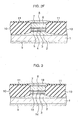
Figs. 2A to 2F are sectional diagrams showing a method for manufacturing the semiconductor laser according to the first embodiment in order of the procedure; -
Fig. 3 is a sectional diagram showing a configuration of an EA modulator according to a second embodiment of the present invention; -
Fig. 4 is a partially sectional diagram showing a configuration of a modulator-integrated semiconductor laser according to a third embodiment of the present invention; -
Fig. 5A is a sectional diagram showing samples produced in an experiment; -
Fig. 5B is a graph showing results of the experiment; and -
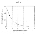
Fig. 6 is a graph showing a relation of concentration ratios r and Zn diffusing widths. - Embodiments of the present invention will be described in detail with reference to the drawings.
- A semiconductor laser according to a first embodiment of the present invention will be described. The semiconductor laser is a semiconductor laser with wavelength of 1.55 µm band to which an SIBH structure is applied.
Fig. 1 is a sectional diagram showing the semiconductor laser according to the first embodiment of the present invention. - In the semiconductor laser, as shown in
Fig. 1 , an n-type clad layer 2 made of n-type InP is formed on an n-type substrate 1 made of n-type InP. On the n-type clad layer 2, anoptical guide layer 3 made of undoped InGaAsP, a multiple quantum wellactive layer 4 made of InGaAsP-series material and having a gain in a 1.55 µm band, and anoptical guide layer 5 made of undoped InGaAsP are layered. On theoptical guide layer 5, a p-type clad layer 6 made of p-type InP or the like and a p+ contact layer 7 made of p+-InGaAsP are layered. The configuration of a layered stack composed of the p+ contact layer 7, the p-type clad layer 6, theoptical guide layer 5, the multiple quantum wellactive layer 4, theoptical guide layer 3 and the n-type clad layer 2 is made as a mesa structure by an etching process. This structure forms a mesa portion. Asemi-insulating burying layer 10 is then provided around the layered stack (mesa portion). The buryinglayer 10 contains Fe as an impurity generating a deep acceptor level. - The thickness of the
optical guide layers active layer 4, for example, well layers made of InGaAsP having a thickness of 5.0 nm and a compressive strain of 0.8% and barrier layers made of lattice-matched InGaAsP having a thickness of 10 nm and a composition of 1.3 µm are layered alternatively. The number of the well layers is 6, for example. - The thickness of the p-type clad
layer 6 is, for example, 1.5 µm and not only Zn of p-type dopant but also Fe is doped thereto. The concentration of Zn is 1.5 x 1018 cm-3 and the concentration of Fe is 1.8 x 1017 cm-3, for example. The thickness of the p+ contact layer 7 is, for example, 300 nm. The concentration of Fe in thesemi-insulating burying layer 10 is 6.0× 1016 cm-3, for example. That is, the concentration of Fe in the p-type cladlayer 6 is three times higher than the concentration of Fe in the buryinglayer 10. - On the burying
layer 10, aninsulation film 11 made of SiO2 or the like and exposing the p+ contact layer 7 is formed. Further, anelectrode 8 contacting with the p+ contact layer 7 and anelectrode 9 contacting with a rear face of the n-type substrate 1 are formed. - In the semiconductor laser having such a structure, since the concentration of Fe doped in the p-type clad
layer 6 is higher than the concentration of Fe doped in the buryinglayer 10, an inter-diffusion of Fe and Zn is suppressed. Thus, leakage current is suppressed while reducing the resistance so that a superior optical output characteristic can be obtained. In other words, since the concentration of Fe doped in the p-type cladlayer 6 is higher than the concentration of Fe doped in the buryinglayer 10, an inter-diffusion of Fe and Zn can be sufficiently suppressed although the p-type cladlayer 6 has a high Zn concentration, which is 1.5 x 1018 cm-3. - Hereinafter, contents and results of experiments actually conducted by the inventors of the present application will be described. In this experiment, samples of four types were produced. In producing those samples, a p-
type InP layer 51 and asemi-insulating InP layer 52 were formed on an n-type InP substrate 50 in order, as shown inFig. 5A . Thesemi-insulating InP layer 52 was a layer containing Fe in a concentration of 6.0 × 1016 cm-3. The p-type InP layer 51 was a layer containing Zn in a concentration of 1.5 × 1018 cm-3 and Fe in a concentration shown in Table 1. The concentration ratios r in Table 1 represent the ratio of the Fe concentration in the p-type InP layer 51 with respect to the Fe concentration in thesemi-insulating InP layer 52. Then, the concentrations of p-type impurity in those four samples were measured. The results are shown inFig. 5B . In this experiment, the p-type impurity concentration is substantially equal to the Zn concentration.[Table 1] Sample No. Fe Concentration Concentration Ratio r 1 0 0 2 6.0 × 1016 cm -31 3 2.4 × 1017 cm -34 4 4.8 8 x 1017 cm -38 - As shown in
Fig. 5B , in case of sample No. 1 of r = 0, the p-type impurity concentration was steeply changed from mid-1017 cm-3 to mid-1016 cm-3 at a position in thesemi-insulating InP layer 52, where is about 0.28 µm spaced from the interface between the p-type InP layer 51 and thesemi-insulating InP layer 52. The p-type impurity concentration was in low-1016 cm-3 in an area farther spaced from the interface. According to this result, it can be considered that the Zn atoms doped in the p-type InP layer 51 diffused into those areas. Here, a mechanism of the diffusion will be studied. - In the sample No. 1, it can be considered that the Zn atoms existed as interstitial atoms (impurity atoms entered into spaces where atoms are not filled) in the p-
type InP layer 51 and the Fe atoms in thesemi-insulating InP layer 52 diffused as exchanging their positions, when thesemi-insulating InP layer 52 was formed. In this inter-diffusion, it is likely that the Zn atoms diffused until its concentration became as the same level as the Fe concentration in thesemi-insulating InP layer 52. This phenomenon is verified inPatent Document 1 and it also occurs when the Zn concentration in the p-type InP layer 51 is low. This diffusion seems to a diffusion of Zn atoms within an area spaced 0.28µm or more from the interface. - Further, in the sample No. 1, since the Zn concentration in the p-
type InP layer 51 is much higher than that of the p-type clad layer described inPatent Document 1, a considerable number of interstitial atoms exist in the p-type InP layer 51, and the atoms are diffused into thesemi-insulating InP layer 52 rapidly. Then, it seems that, in thesemi-insulating InP layer 52, the Zn atoms were introduced into In vacancies or introduced into lattice sites by pushing Indium out of the lattice sites, and that the Zn atoms became substitutional impurity atoms (impurity atoms occupying lattice sites). In this way, it is considered that, because of such an excessive diffusion of the interstitial atoms (Zn atoms), the number of substitutional impurity atoms (Zn atoms) inserted into the lattice sites in thesemi-insulating InP layer 52 is increased. This diffusion seems to be a diffusion of Zn atoms within an area near the interface. - As described above, in the sample No. 1, since a great number of Zn atoms were diffused into the
semi-insulating InP layer 52, a leakage current is increased and an optical output characteristic is deteriorated. - In case of sample No. 2, Fe in the same concentration was doped to the p-
type InP layer 51 and thesemi-insulating InP layer 52 but the Zn concentration in the p-type InP layer 51 was much higher than the p-type clad layer described inPatent Document 1. Thus, as shown inFig. 5B , a diffusion of Zn atoms into thesemi-insulating InP layer 52 was observed although the degree of the diffusion was reduced compared to the case of sample No. 1. As a result, in case of the sample No. 2, also, a leakage current is increased and an optical output characteristic is deteriorated. - On the other hand, in case of sample No. 3, since the concentration of Fe doped in the p-
type InP layer 51 was four times higher than that in thesemi-insulating InP layer 52, a diffusion of Zn atoms into thesemi-insulating InP layer 52 was remarkably suppressed, as shown inFig. 5B . That is, the p-type impurity concentration profile, which is substantially equal to the concentration profile of Zn atoms, was steep near the interface between the p-type InP layer 51 and thesemi-insulating InP layer 52. Thus, in case of the sample No. 3, a leakage current is suppressed and a superior optical output characteristic is obtained. - In case of sample No. 4, since the concentration of Fe doped in the p-
type InP layer 51 was eight times higher than that in thesemi-insulating InP layer 52, a diffusion of Zn atoms into thesemi-insulating InP layer 52 was further suppressed, as shown inFig. 5B . Thus, also in case of the sample No. 4, a leakage current is suppressed and a superior optical output characteristic is obtained. - According to these results, inter-diffusion of Fe and Zn can be suppressed when Fe with higher concentration is doped in the p-
type InP layer 51 than thesemi-insulating InP layer 52. Then, compared to the first embodiment, since the p-type InP layer 51 corresponds to the p-type cladlayer 6, and thesemi-insulating InP layer 52 corresponds to the buryinglayer 10, the experiment results proved the suppression of the inter-diffusion of Fe and Zn in the first embodiment. - Further, based on the graph shown in
Fig. 5B , assuming a width of an area in which the Zn atoms became substitutional impurity atoms in thesemi-insulating InP layer 52 from the interface as a Zn diffusing width, when a relation between the Zn diffusing width and the concentration ratio r is illustrated, a graph inFig. 6 is obtained. In order to reduce a leakage current, preferably, the Zn diffusing width is made 0.1 µm or less. According to the graph inFig. 6 , the Zn diffusing width can be suppressed within in the range when the concentration ratio r is 2 or more. Further, according to the graph inFig. 6 , the 2n diffusing width seems to be reduced as the concentration ratio r becomes larger; however, in case of the sample No. 4 (r = 8), introduction of the Fe atoms into the lattice site reached a saturated state and a part of the Fe atoms precipitated in the p-type InP layer 51. With this result, the effect of the present invention can be saturated even if the concentration ratio r is set more than 8. The concentration ratio r is thus preferable to be from 2 to 8. - A method for manufacturing the semiconductor laser according to the first embodiment will be described.
Figs. 2A to 2F are sectional diagrams showing a method for manufacturing the semiconductor laser according to the first embodiment in order of the procedure. - As shown in
Fig. 2A , using a Metal-Organic Vapor Phase Epitaxy method (MOVPE method), the n-type cladlayer 2, theoptical guide layer 3, the multiple quantum wellactive layer 4, theoptical guide layer 5, the p-type cladlayer 6 and the p+ contact layer 7 are formed on the n-type substrate 1. When the p-type cladlayer 6 is formed, Zn in a concentration of 1.5 x 1018 cm-3 and Fe in concentration of 1.8 x 1017 cm-3 are doped. - Then, as shown in
Fig. 2B , astriped mask 31 is formed on the p+ contact layer 7. - Thereafter, using the
mask 31, an etching such as an Inductive Coupled Plasma Reactive Ion Etching (ICP-RIE) is executed. As a result, as shown inFig. 2C , a mesa structure is made with a layered stack composed of the p+ contact layer 7, the p-type cladlayer 6, theoptical guide layer 5, the multiple quantum wellactive layer 4, theoptical guide layer 3 and the n-type cladlayer 2. - Next, as shown in
Fig. 2D , asemi-insulating burying layer 10 is provided around the layered stack of the mesa structure. With this procedure, a current confinement structure is obtained. Here, when the buryinglayer 10 is formed, Fe in a concentration of 6.0 x 1016 cm-3 is doped. That is, the concentration ratio r is made to be 3. - Then, as shown in
Fig. 2E , themask 31 is removed and theinsulation film 11 exposing the p+ contact layer 7 is formed. - Thereafter, as shown in
Fig. 2F , theelectrode 8 contacting with the p+ contact layer 7 and theelectrode 9 contacting with the rear face of the n-type substrate 1 are formed. - In this explanation of the manufacturing method, the concentration ratio r is made to be 3; however, the concentration ratio r can be any number if it is greater than 1 and, preferably, from 2 to 8.
- An electro-absorption modulator (EA modulator) according to a second embodiment of the present invention will be described.
Fig. 3 is a sectional diagram showing the EA modulator according to the second embodiment of the present invention. - In this EA modulator, as shown in
Fig. 3 , alight absorption layer 14 made of InGaAsP-series material is provided as a substitute for the quantum well active layeractive layer 4 in the first embodiment, and anoptical guide layer 15 made of undoped InGaAsP is provided as a substitute for theoptical guide layer 5 in the first embodiment. In thelight absorption layer 14, for example, well layers made of InGaAsP having a thickness of 9.0 nm and a compressive strain of 0.5% and barrier layers made of InGaAsP having a thickness of 5.0 nm, a composition of 1.3 µm and tensile strain of 0.3% are layered alternatively. In other words, thelight absorption layer 14 has a multiple quantum well structure. The number of the well layers is 6, for example. Here, although the transition wavelength of the multiple quantum well structure in thelight absorption layer 14 is not limited, when an input wavelength is 1.55 µm, for example, the transition wavelength can be set about from 1.49 µm to 1.50 µm. Further, the thickness of theoptical guide layer 15 is 50 nm and its composition is continuously changing between 1.15 µm and 1.00 µm, for example. In other words, the composition of theoptical guide layer 15 at the interface with thelight absorption layer 14 is 1.15 µm, the composition of theoptical guide layer 15 at the interface with the p-type cladlayer 6 is 1.00 µm, and accordingly, theoptical guide layer 15 is a graded layer. Other structures are same as those in the first embodiment. - In the EA modulator having the above structure, also, since the Fe concentration is higher in the p-type clad
layer 6 than the buryinglayer 10, an inter-diffusion of Fe and Zn is suppressed. Thus, a wide bandwidth can be assured as reducing the resistance and a superior modulation characteristic can be obtained. - A modulator-integrated semiconductor laser according to a third embodiment of the present invention will be described.
Fig. 4 is a partially sectional diagram showing a configuration of the modulator-integrated semiconductor laser according to the third embodiment of the present invention. - In this modulator-integrated semiconductor laser, as shown in
Fig. 4 , asemiconductor laser 31 same as the first embodiment and anEA modulator 32 same as the second embodiment are integrated by a butt-joint connection. Here, in thesemiconductor laser 31, alight emitting portion 21 composed of theoptical guide layer 3, the multiple quantum wellactive layer 4 and theoptical guide layer 5 are formed and adiffraction grating 22 is formed at the bottom of thelight emitting portion 21. Thesemiconductor laser 31 thus oscillates in a single mode. Further, in theEA modulator 32, amodulation unit 23 composed of theoptical guide layer 3, thelight absorption layer 14 and the optical 1guide layer 15 are formed. - According to the modulator-integrated semiconductor laser having such a configuration, the effects of the both first and second embodiments can be obtained. In other words, a superior optical output characteristic and wide modulation bandwidth can be attained while reducing the resistance.
- In the first and third embodiments, the multiple quantum well
active layer 4 having a gain in 1.55µm band is made of In1-xGaxAsyP1-y-series (0 ≦ x, y ≦ 1) material; however, it can be made of other materials such as InxGayAl1-x-yAs-series (0 ≦ x, y ≦ 1) material. In this case, in the multiple quantum wellactive layer 4, for example, well layers made of InGaAlAs having a thickness of 5.0 nm and a compressive strain of 1.0% and barrier layers made of InGaAlAs having a thickness of 10 nm, a composition of 1.2 µm and a tensile strain of 0.3% are layered alternatively. The number of the well layers is 6, for example. - Further, for example, a layer made of undoped InGaAlAs having a thickness of 50 nm and a composition 1.2 µm is used as the
optical guide layer 3 under the multiple quantum wellactive layer 4. Furthermore, for example, a layer made of undoped InGaAsP having a thickness of 50 nm and a composition of 1.05 µm is used as theoptical guide layer 5 on the multiple quantum wellactive layer 4. - According to the semiconductor laser having such a multiple quantum well
active layer 4 made of InGaAlAs-series material, a band offset of a conduction band in the quantum well structure is larger, compared to the first embodiment having a multiple quantum wellactive layer 4 made of InGaAsP-series material. Thus, compared to the first embodiment, the electron confinement is improved and superior high-temperature characteristics are obtained. - Here, in the EA modulator and the like, InxGayAl1-x-yAs-series (0 ≦ x, y ≦ 1) material can be employed.
- Further, the p-type impurity added to the p-type clad
layer 6 is not limited to Zn, and Cd and/or Mg can be added, for example. The concentrations of those p-type impurities are preferably equal to or more than 1.0 × 1018 cm-3 in order to reduce the resistance. Further, the impurity generating a deep acceptor level added to the buryinglayer 10 and p-type cladlayer 6 is not limited to Fe, and Co and/or Cu can be added. - Also, a GaAs layer or the like can be included as a part of the p-type clad
layer 6 and the buryinglayer 10. When the p-type cladlayer 6 and the buryinglayer 10 are formed, for example, only an InP layer can be formed, or a thin GaAs may be formed first and an InP layer may be formed thereon. - The above embodiments relate to semiconductor optical devices (semiconductor laser and semiconductor EA modulator) having a burying layer and a mesa portion including a p-type semiconductor layer formed on a semiconductor substrate; however, the present invention is not limited to the structure. The present invention can be applied to, for example, a semiconductor optical device having the same structure as a semiconductor optical amplifier and a Mach-Zehnder type optical modulator.
- According to an embodiment of the present invention, since an impurity in a higher concentration is applied to a p-type semiconductor layer than a burying layer, unnecessary diffusions of p-type impurity in the p-type semiconductor layer can be suppressed.
- The foregoing is considered as illustrative only of the principles of the present invention. Further, since numerous modifications and changes will readily occur to those skilled in the art, it is not desired to limit the invention to the exact construction and applications shown and described, and accordingly, all suitable modifications and equivalents may be regarded as falling within the scope of the invention in the appended claims and their equivalents.
Claims (20)
- A semiconductor optical device comprising:a semiconductor substrate;a mesa portion formed on said semiconductor substrate and including a p-type semiconductor layer to which a p-type impurity is added; anda burying layer burying said mesa portion and made of a group III-V compound semiconductor to which an impurity generating a deep acceptor level is added,wherein said p-type semiconductor layer has a higher concentration of the impurity generating a deep acceptor level, compared to said burying layer.
- The semiconductor optical device according to claim 1, wherein a concentration of the impurity forming a deep acceptor level in the p-type semiconductor layer is 2 to 8 times higher than a concentration of the impurity forming a deep acceptor level in said burying layer.
- The semiconductor optical device according to claim 1 or 2, wherein a concentration of the p-type impurity in the p-type semiconductor layer is equal to or greater than 1.0 x 1018 cm-3.
- The semiconductor optical device according to claim 1, 2 or 3, wherein the p-type impurity is at least one type selected from a group consisting of Zn, Cd and Mg.
- The semiconductor optical device according to any preceding claim, wherein the p-type semiconductor layer is made of a group III-V compound semiconductor.
- The semiconductor optical device according to any preceding claim, wherein said burying layer comprises at least an InP layer.
- The semiconductor optical device according to any preceding claim, wherein the p-type semiconductor layer comprises at least an InP layer.
- The semiconductor optical device according to any preceding claim, wherein the impurity forming a deep acceptor level is at least one type selected from a group consisting of Fe, Co and Cu.
- The semiconductor optical device according to any preceding claim, wherein said semiconductor substrate is an InP substrate having an n-type conductivity.
- The semiconductor optical device according to any preceding claim, wherein said mesa portion comprises an active layer made of In1-xGaxAsyP1-y-series (0≦x, y≦1) material or InxGayAl1-x-yAs-series (0 ≦x, y≦1) material.
- The semiconductor optical device according to any preceding claim, which serves as a semiconductor laser.
- The semiconductor optical device according to any one of claims 1' to 10, which serves as an electro-absorption semiconductor optical modulator.
- The semiconductor optical device according to any one of claims 1 to 10, which serves as an integrated electro-absorption semiconductor optical modulator and a semiconductor laser.
- A manufacturing method of a semiconductor optical device, comprising the steps of:forming a mesa portion on a semiconductor substrate, the mesa portion including a p-type semiconductor layer to which a p-type impurity is added; andforming a burying layer burying the mesa portion and made of a group III-V compound semiconductor to which an impurity generating a deep acceptor level is added,wherein a layer having a higher concentration of the impurity generating a deep acceptor level, compared to the burying layer, is formed as the p-type semiconductor layer.
- The manufacturing method of a semiconductor optical device according to claim 14, wherein a concentration of the impurity generating a deep acceptor level in the p-type semiconductor layer is made 2 to 8 times higher than a concentration of the impurity forming a deep acceptor level in the burying layer.
- The manufacturing method of a semiconductor optical device according to claim 14 or 15, wherein the concentration of the p-type impurity in the p-type semiconductor layer is made equal to or greater than 1.0 x 1018 cm-3.
- The manufacturing method of a semiconductor optical device according to claim 14, 15 or 16, wherein, as the p-type impurity, at least one type selected from a group consisting of Zn, Cd and Mg is used.
- The manufacturing method of a semiconductor optical device according to claim 14, 15, 16 or 17, wherein, as the burying layer, at least an InP layer is formed.
- The manufacturing method of a semiconductor optical device according to any one of claims 14 to 18, wherein, as the p-type semiconductor layer, at least an InP layer is formed.
- The manufacturing method of a semiconductor optical device according to any one of claims 14 to 19, wherein, as the impurity generating a deep acceptor level, at least one type selected from a group consisting of Fe, Co and Cu is used.
Applications Claiming Priority (1)
| Application Number | Priority Date | Filing Date | Title |
|---|---|---|---|
| JP2007084593A JP2008244264A (en) | 2007-03-28 | 2007-03-28 | Semiconductor optical device and manufacturing method thereof |
Publications (1)
| Publication Number | Publication Date |
|---|---|
| EP1981138A1 true EP1981138A1 (en) | 2008-10-15 |
Family
ID=39671888
Family Applications (1)
| Application Number | Title | Priority Date | Filing Date |
|---|---|---|---|
| EP08152599A Withdrawn EP1981138A1 (en) | 2007-03-28 | 2008-03-11 | Semiconductor optical device and manufacturing method thereof |
Country Status (3)
| Country | Link |
|---|---|
| US (1) | US7804870B2 (en) |
| EP (1) | EP1981138A1 (en) |
| JP (1) | JP2008244264A (en) |
Families Citing this family (6)
| Publication number | Priority date | Publication date | Assignee | Title |
|---|---|---|---|---|
| JP5660940B2 (en) | 2010-04-27 | 2015-01-28 | 住友電工デバイス・イノベーション株式会社 | Manufacturing method of optical semiconductor device |
| JP5545670B2 (en) * | 2010-04-27 | 2014-07-09 | 住友電工デバイス・イノベーション株式会社 | Optical semiconductor device and manufacturing method thereof |
| JP6209843B2 (en) * | 2013-03-29 | 2017-10-11 | 住友電気工業株式会社 | Method for manufacturing semiconductor modulator, semiconductor modulator |
| JP6236947B2 (en) * | 2013-07-16 | 2017-11-29 | 住友電気工業株式会社 | Method for manufacturing semiconductor optical device, and semiconductor optical device |
| US10833480B2 (en) * | 2018-07-03 | 2020-11-10 | Skorpios Technologies, Inc. | Diffusion blocking layer for a compound semiconductor structure |
| JP7306779B2 (en) * | 2019-09-13 | 2023-07-11 | 住友電工デバイス・イノベーション株式会社 | OPTO-SEMICONDUCTOR DEVICE AND MANUFACTURING METHOD THEREOF |
Citations (5)
| Publication number | Priority date | Publication date | Assignee | Title |
|---|---|---|---|---|
| JPH0637392A (en) * | 1992-07-17 | 1994-02-10 | Fujitsu Ltd | Semiconductor laser |
| GB2293485A (en) * | 1994-09-26 | 1996-03-27 | Mitsubishi Electric Corp | Semiconductor device |
| GB2364600A (en) * | 2000-01-07 | 2002-01-30 | Lucent Technologies Inc | Dopant diffusion barrier having more than one layer and not forming a pn junction with an adjacent layer |
| US6556605B1 (en) * | 2000-02-29 | 2003-04-29 | Triquent Technology Holding, Co. | Method and device for preventing zinc/iron interaction in a semiconductor laser |
| US20060054916A1 (en) * | 2004-09-14 | 2006-03-16 | Mitsubishi Denki Kabushiki Kaisha | Optical semiconductor device and method of fabricating optical semiconductor device |
Family Cites Families (6)
| Publication number | Priority date | Publication date | Assignee | Title |
|---|---|---|---|---|
| JPH06104532A (en) * | 1992-09-21 | 1994-04-15 | Nippon Telegr & Teleph Corp <Ntt> | Compound semiconductor thin film |
| FR2706079B1 (en) * | 1993-06-02 | 1995-07-21 | France Telecom | Integrated laser-modulator monolithic component with quantum multi-well structure. |
| JP2697615B2 (en) * | 1994-07-07 | 1998-01-14 | 日本電気株式会社 | Multiple quantum well semiconductor laser |
| JP3809941B2 (en) | 2001-10-03 | 2006-08-16 | 日本電信電話株式会社 | Electroabsorption optical modulator |
| US6891202B2 (en) * | 2001-12-14 | 2005-05-10 | Infinera Corporation | Oxygen-doped Al-containing current blocking layers in active semiconductor devices |
| JP2008053649A (en) * | 2006-08-28 | 2008-03-06 | Mitsubishi Electric Corp | Embedded semiconductor laser |
-
2007
- 2007-03-28 JP JP2007084593A patent/JP2008244264A/en active Pending
-
2008
- 2008-03-11 EP EP08152599A patent/EP1981138A1/en not_active Withdrawn
- 2008-03-21 US US12/053,213 patent/US7804870B2/en not_active Expired - Fee Related
Patent Citations (5)
| Publication number | Priority date | Publication date | Assignee | Title |
|---|---|---|---|---|
| JPH0637392A (en) * | 1992-07-17 | 1994-02-10 | Fujitsu Ltd | Semiconductor laser |
| GB2293485A (en) * | 1994-09-26 | 1996-03-27 | Mitsubishi Electric Corp | Semiconductor device |
| GB2364600A (en) * | 2000-01-07 | 2002-01-30 | Lucent Technologies Inc | Dopant diffusion barrier having more than one layer and not forming a pn junction with an adjacent layer |
| US6556605B1 (en) * | 2000-02-29 | 2003-04-29 | Triquent Technology Holding, Co. | Method and device for preventing zinc/iron interaction in a semiconductor laser |
| US20060054916A1 (en) * | 2004-09-14 | 2006-03-16 | Mitsubishi Denki Kabushiki Kaisha | Optical semiconductor device and method of fabricating optical semiconductor device |
Also Published As
| Publication number | Publication date |
|---|---|
| JP2008244264A (en) | 2008-10-09 |
| US7804870B2 (en) | 2010-09-28 |
| US20080240191A1 (en) | 2008-10-02 |
Similar Documents
| Publication | Publication Date | Title |
|---|---|---|
| US7835413B2 (en) | Semiconductor laser | |
| JP3654435B2 (en) | Semiconductor optical device and manufacturing method thereof | |
| EP0475330B1 (en) | Ridge-waveguide buried heterostructure laser and method of fabrication | |
| EP0959540B1 (en) | Semiconductor laser having effective output increasing function | |
| EP0575684A1 (en) | Decoupled optic and electronic confinement laser diode | |
| EP1251610B1 (en) | Semiconductor optical device and the fabrication method | |
| US7804870B2 (en) | Semiconductor optical device and manufacturing method thereof | |
| JP4057802B2 (en) | Semiconductor optical device | |
| US6798552B2 (en) | Semiconductor light modulator | |
| EP1750336A1 (en) | Semiconductor optical device and a method of fabricating the same | |
| US20040075154A1 (en) | Waveguide photodiode | |
| US6819695B1 (en) | Dopant diffusion barrier layer for use in III-V structures | |
| EP1320158A1 (en) | Means of controlling dopant diffusion in a semiconductor heterostructure | |
| JP2005209909A (en) | Semiconductor optical device and manufacturing method thereof | |
| JPH07193321A (en) | Manufacture of semiconductor laser | |
| JP3307669B2 (en) | Compound semiconductor superlattice | |
| US7298769B2 (en) | Semiconductor laser | |
| JP3645343B2 (en) | Semiconductor laser element | |
| JPH0945989A (en) | Semiconductor laser device | |
| JP2005260109A (en) | Optical semiconductor device | |
| US20080013579A1 (en) | Buried-heterostructure semiconductor laser | |
| JP3213428B2 (en) | Semiconductor laser device and method of manufacturing the same | |
| JPH07131116A (en) | Semiconductor laser device | |
| JPH088482A (en) | Semiconductor laser and manufacture thereof | |
| JPH06244492A (en) | Semiconductor laser |
Legal Events
| Date | Code | Title | Description |
|---|---|---|---|
| PUAI | Public reference made under article 153(3) epc to a published international application that has entered the european phase |
Free format text: ORIGINAL CODE: 0009012 |
|
| AK | Designated contracting states |
Kind code of ref document: A1 Designated state(s): AT BE BG CH CY CZ DE DK EE ES FI FR GB GR HR HU IE IS IT LI LT LU LV MC MT NL NO PL PT RO SE SI SK TR |
|
| AX | Request for extension of the european patent |
Extension state: AL BA MK RS |
|
| 17P | Request for examination filed |
Effective date: 20090414 |
|
| AKX | Designation fees paid |
Designated state(s): DE FR GB |
|
| 17Q | First examination report despatched |
Effective date: 20100317 |
|
| STAA | Information on the status of an ep patent application or granted ep patent |
Free format text: STATUS: THE APPLICATION HAS BEEN WITHDRAWN |
|
| 18W | Application withdrawn |
Effective date: 20140325 |