EP1980903A2 - Liquid crystal display device and method of fabricating the same - Google Patents
Liquid crystal display device and method of fabricating the same Download PDFInfo
- Publication number
- EP1980903A2 EP1980903A2 EP07025120A EP07025120A EP1980903A2 EP 1980903 A2 EP1980903 A2 EP 1980903A2 EP 07025120 A EP07025120 A EP 07025120A EP 07025120 A EP07025120 A EP 07025120A EP 1980903 A2 EP1980903 A2 EP 1980903A2
- Authority
- EP
- European Patent Office
- Prior art keywords
- liquid crystal
- passivation film
- substrate
- display device
- crystal display
- Prior art date
- Legal status (The legal status is an assumption and is not a legal conclusion. Google has not performed a legal analysis and makes no representation as to the accuracy of the status listed.)
- Granted
Links
Images














Classifications
-
- G—PHYSICS
- G02—OPTICS
- G02F—OPTICAL DEVICES OR ARRANGEMENTS FOR THE CONTROL OF LIGHT BY MODIFICATION OF THE OPTICAL PROPERTIES OF THE MEDIA OF THE ELEMENTS INVOLVED THEREIN; NON-LINEAR OPTICS; FREQUENCY-CHANGING OF LIGHT; OPTICAL LOGIC ELEMENTS; OPTICAL ANALOGUE/DIGITAL CONVERTERS
- G02F1/00—Devices or arrangements for the control of the intensity, colour, phase, polarisation or direction of light arriving from an independent light source, e.g. switching, gating or modulating; Non-linear optics
- G02F1/01—Devices or arrangements for the control of the intensity, colour, phase, polarisation or direction of light arriving from an independent light source, e.g. switching, gating or modulating; Non-linear optics for the control of the intensity, phase, polarisation or colour
- G02F1/13—Devices or arrangements for the control of the intensity, colour, phase, polarisation or direction of light arriving from an independent light source, e.g. switching, gating or modulating; Non-linear optics for the control of the intensity, phase, polarisation or colour based on liquid crystals, e.g. single liquid crystal display cells
- G02F1/133—Constructional arrangements; Operation of liquid crystal cells; Circuit arrangements
- G02F1/1333—Constructional arrangements; Manufacturing methods
- G02F1/1339—Gaskets; Spacers; Sealing of cells
- G02F1/13394—Gaskets; Spacers; Sealing of cells spacers regularly patterned on the cell subtrate, e.g. walls, pillars
-
- G—PHYSICS
- G02—OPTICS
- G02F—OPTICAL DEVICES OR ARRANGEMENTS FOR THE CONTROL OF LIGHT BY MODIFICATION OF THE OPTICAL PROPERTIES OF THE MEDIA OF THE ELEMENTS INVOLVED THEREIN; NON-LINEAR OPTICS; FREQUENCY-CHANGING OF LIGHT; OPTICAL LOGIC ELEMENTS; OPTICAL ANALOGUE/DIGITAL CONVERTERS
- G02F1/00—Devices or arrangements for the control of the intensity, colour, phase, polarisation or direction of light arriving from an independent light source, e.g. switching, gating or modulating; Non-linear optics
- G02F1/01—Devices or arrangements for the control of the intensity, colour, phase, polarisation or direction of light arriving from an independent light source, e.g. switching, gating or modulating; Non-linear optics for the control of the intensity, phase, polarisation or colour
- G02F1/13—Devices or arrangements for the control of the intensity, colour, phase, polarisation or direction of light arriving from an independent light source, e.g. switching, gating or modulating; Non-linear optics for the control of the intensity, phase, polarisation or colour based on liquid crystals, e.g. single liquid crystal display cells
- G02F1/133—Constructional arrangements; Operation of liquid crystal cells; Circuit arrangements
- G02F1/1333—Constructional arrangements; Manufacturing methods
- G02F1/1339—Gaskets; Spacers; Sealing of cells
-
- G—PHYSICS
- G02—OPTICS
- G02F—OPTICAL DEVICES OR ARRANGEMENTS FOR THE CONTROL OF LIGHT BY MODIFICATION OF THE OPTICAL PROPERTIES OF THE MEDIA OF THE ELEMENTS INVOLVED THEREIN; NON-LINEAR OPTICS; FREQUENCY-CHANGING OF LIGHT; OPTICAL LOGIC ELEMENTS; OPTICAL ANALOGUE/DIGITAL CONVERTERS
- G02F1/00—Devices or arrangements for the control of the intensity, colour, phase, polarisation or direction of light arriving from an independent light source, e.g. switching, gating or modulating; Non-linear optics
- G02F1/01—Devices or arrangements for the control of the intensity, colour, phase, polarisation or direction of light arriving from an independent light source, e.g. switching, gating or modulating; Non-linear optics for the control of the intensity, phase, polarisation or colour
- G02F1/13—Devices or arrangements for the control of the intensity, colour, phase, polarisation or direction of light arriving from an independent light source, e.g. switching, gating or modulating; Non-linear optics for the control of the intensity, phase, polarisation or colour based on liquid crystals, e.g. single liquid crystal display cells
- G02F1/133—Constructional arrangements; Operation of liquid crystal cells; Circuit arrangements
- G02F1/136—Liquid crystal cells structurally associated with a semi-conducting layer or substrate, e.g. cells forming part of an integrated circuit
-
- G—PHYSICS
- G02—OPTICS
- G02F—OPTICAL DEVICES OR ARRANGEMENTS FOR THE CONTROL OF LIGHT BY MODIFICATION OF THE OPTICAL PROPERTIES OF THE MEDIA OF THE ELEMENTS INVOLVED THEREIN; NON-LINEAR OPTICS; FREQUENCY-CHANGING OF LIGHT; OPTICAL LOGIC ELEMENTS; OPTICAL ANALOGUE/DIGITAL CONVERTERS
- G02F1/00—Devices or arrangements for the control of the intensity, colour, phase, polarisation or direction of light arriving from an independent light source, e.g. switching, gating or modulating; Non-linear optics
- G02F1/01—Devices or arrangements for the control of the intensity, colour, phase, polarisation or direction of light arriving from an independent light source, e.g. switching, gating or modulating; Non-linear optics for the control of the intensity, phase, polarisation or colour
- G02F1/13—Devices or arrangements for the control of the intensity, colour, phase, polarisation or direction of light arriving from an independent light source, e.g. switching, gating or modulating; Non-linear optics for the control of the intensity, phase, polarisation or colour based on liquid crystals, e.g. single liquid crystal display cells
- G02F1/133—Constructional arrangements; Operation of liquid crystal cells; Circuit arrangements
- G02F1/1333—Constructional arrangements; Manufacturing methods
- G02F1/1339—Gaskets; Spacers; Sealing of cells
- G02F1/13396—Spacers having different sizes
-
- G—PHYSICS
- G02—OPTICS
- G02F—OPTICAL DEVICES OR ARRANGEMENTS FOR THE CONTROL OF LIGHT BY MODIFICATION OF THE OPTICAL PROPERTIES OF THE MEDIA OF THE ELEMENTS INVOLVED THEREIN; NON-LINEAR OPTICS; FREQUENCY-CHANGING OF LIGHT; OPTICAL LOGIC ELEMENTS; OPTICAL ANALOGUE/DIGITAL CONVERTERS
- G02F1/00—Devices or arrangements for the control of the intensity, colour, phase, polarisation or direction of light arriving from an independent light source, e.g. switching, gating or modulating; Non-linear optics
- G02F1/01—Devices or arrangements for the control of the intensity, colour, phase, polarisation or direction of light arriving from an independent light source, e.g. switching, gating or modulating; Non-linear optics for the control of the intensity, phase, polarisation or colour
- G02F1/13—Devices or arrangements for the control of the intensity, colour, phase, polarisation or direction of light arriving from an independent light source, e.g. switching, gating or modulating; Non-linear optics for the control of the intensity, phase, polarisation or colour based on liquid crystals, e.g. single liquid crystal display cells
- G02F1/133—Constructional arrangements; Operation of liquid crystal cells; Circuit arrangements
- G02F1/136—Liquid crystal cells structurally associated with a semi-conducting layer or substrate, e.g. cells forming part of an integrated circuit
- G02F1/1362—Active matrix addressed cells
- G02F1/136227—Through-hole connection of the pixel electrode to the active element through an insulation layer
-
- G—PHYSICS
- G02—OPTICS
- G02F—OPTICAL DEVICES OR ARRANGEMENTS FOR THE CONTROL OF LIGHT BY MODIFICATION OF THE OPTICAL PROPERTIES OF THE MEDIA OF THE ELEMENTS INVOLVED THEREIN; NON-LINEAR OPTICS; FREQUENCY-CHANGING OF LIGHT; OPTICAL LOGIC ELEMENTS; OPTICAL ANALOGUE/DIGITAL CONVERTERS
- G02F2201/00—Constructional arrangements not provided for in groups G02F1/00 - G02F7/00
- G02F2201/50—Protective arrangements
Definitions
- the present invention relates to a liquid crystal display device and a method of fabricating the same.
- liquid crystal display LCD liquid crystal display LCD
- plasma display panel PDP field emission display FED
- vacuum fluorescent display VFD vacuum fluorescent display VFD
- the liquid crystal display LCD has attracted great attentions owing to the advantages of mass production, simple driving means and high resolution and picture quality.
- FIG. 1 is a cross section view illustrating a liquid crystal display device according to the related art.
- the liquid crystal display device according to the related art includes a lower substrate 5, an upper substrate 3, and a liquid crystal layer 7 formed between the lower substrate 5 and the upper substrate 3.
- the lower substrate 5 corresponds to a thin film transistor array substrate, which includes a plurality of pixel regions, wherein a thin film transistor is formed in each of the pixel region.
- the upper substrate 3 corresponds to a color filter substrate, which includes a color filter layer to realize colors.
- pixel electrodes and a common electrode are formed on the lower substrate 5 and the upper substrate 3, respectively.
- the lower and upper substrates 5 and 3 are coated with alignment films to align liquid crystal molecules included in the liquid crystal layer 7.
- spacers 9 are provided between the lower substrate 5 and the upper substrate 3, to maintain a cell gap therebetween.
- the liquid crystal layer 7 is formed between the lower substrate 5 and the upper substrate 3. According as the liquid crystal molecules included in the liquid crystal layer 7 are driven by the thin film transistor formed on the lower substrate 5, an amount of light passing through the liquid crystal layer is controlled so that information is displayed.
- the liquid crystal display device uses electro-optic effects which are determined based on anisotropy of liquid crystal and alignment of liquid crystal molecules.
- the display stability in the liquid crystal display device is largely affected by the control for the alignment of liquid crystal molecules.
- the processes of forming the alignment film to align the liquid crystal molecules and forming the spacers to maintain the cell gap with a seal pattern are greatly related with the picture quality in the liquid crystal cell.
- the spacers exist in the pixel region through which light transmits.
- the spacers existing in the pixel region may disturb the alignment of liquid crystal, and lower an aperture ratio.
- the density of spacers has to be controlled under a predetermined level. Also, it is necessary to obtain the uniformity in providing the spacers on an entire screen.
- a contrast ratio may be lowered due to deterioration of a black display function since the spacer causes dispersion of light and disorder of alignment in its circumference.
- the column spacer can be fabricated by steps of depositing or coating organic polymer material on a substrate and carrying out photolithography to selectively remove the deposited or coated organic polymer material.
- the photolithography is comprised of coating, exposure and development of photoresist, so that it necessarily requires an additional mask, thereby causing the complicated process and increasing cost.
- the present invention is directed to a liquid crystal display device and a method of fabricating the same that substantially obviates one or more problems due to limitations and disadvantages of the related art.
- An object of the present invention is to provide a liquid crystal display device to simplify the process and decrease the fabrication cost, and a method of fabricating the same.
- a liquid crystal display device comprises a first substrate having a color filter and a second substrate having a thin film transistor, wherein the first and second substrates are facing each other; a first passivation film formed on the thin film transistor; and a first column spacer formed as one body with the first passivation film.
- the first column spacer is brought into contact with the first substrate.
- the device comprises a second column spacer formed as one body with the first passivation film.
- first and second column spacers have the different heights from each other.
- first passivation film and the first and second column spacers are formed of an organic insulation material comprised of ultra-violet curable liquid pre-polymer, photo-initiator and surfactant.
- the device comprises a second passivation film between the thin film transistor and the first passivation film.
- the device comprises a third passivation film on the first passivation film.
- the second and third passivation films are formed of an inorganic insulation material.
- the second substrate comprises gate and data lines crossing each other to define a pixel region on the second substrate; and a pixel electrode connected to a predetermined portion of the thin film transistor and formed in the pixel region, and a liquid crystal layer formed between the first and second substrates.
- a method of fabricating a liquid crystal display device comprises preparing a first substrate having a color filter; forming a thin film transistor on a second substrate facing the first substrate; forming a pattern material layer on the second substrate including the thin film transistor; aligning a soft mold and the second substrate including the pattern material layer; forming a contact hole, a first passivation film and a first column spacer by contacting the soft mold to the pattern material layer; separating the soft mold from the pattern material layer; and forming a pixel electrode in the contact hole.
- the pattern material layer is formed of an organic insulation material comprised of ultra-violet curable liquid pre-polymer, photo-initiator and surfactant.
- the soft mold is provided with embossing patterns for formation of the contact hole, and depressed patterns for formation of the column spacer.
- the soft mold is formed of any one of DMS (polydimethylsiloxane), polyurethane or polyimide.
- the method comprises curing the pattern material layer by applying heat or light to the substrate in state of contacting the soft mold to the substrate including the pattern material layer.
- the method comprises forming a second column spacer when forming the contact hole, the first passivation film and the first column spacer.
- the first column spacer has such a height as to contact with the first substrate, and the second column spacer is different from the first column spacer in height.
- the soft mold is provided with depressed patterns for formation of the second column spacer.
- the method comprises forming a second passivation film between the pattern material layer and the substrate including the thin film transistor.
- the method comprises forming a third passivation film between the first passivation film and the pixel electrode.
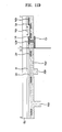
- FIG. 1 is a cross section diagram illustrating a related art liquid crystal display device
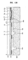
- FIG. 2 is a plan diagram illustrating one liquid crystal display device according to the present invention.
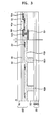
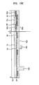
- FIG. 3 is a cross section diagram illustrating a liquid crystal display device according to the first embodiment of the present invention, along I-I' and II-II' of FIG. 2 ;
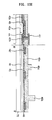
- FIGs. 4A to 4D are cross section diagrams illustrating a method of fabricating a liquid crystal display device according to the first embodiment of the present invention
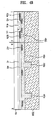
- FIG. 5 is a cross section diagram illustrating a liquid crystal display device according to the second embodiment of the present invention, along I-I' and II-II' of FIG. 2 ;
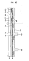
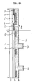
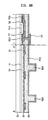
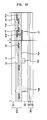
- FIGs. 6A to 6E are cross section diagrams illustrating a method of fabricating a liquid crystal display device according to the second embodiment of the present invention.
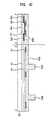
- FIG. 7 is a cross section diagram illustrating a liquid crystal display device according to the third embodiment of the present invention, along I-I' and II-II' of FIG. 2 ;
- FIGs. 8A to 8B are cross section diagrams illustrating a method of fabricating a liquid crystal display device according to the third embodiment of the present invention.
- FIG. 9 is a plan diagram illustrating another liquid crystal display device according to the present invention.
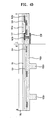
- FIG. 10 is a cross section diagram illustrating a liquid crystal display device according to the fourth embodiment of the present invention, along I-I' and II-II' of FIG. 9 ;
- FIGs. 11A to 11D are cross section diagrams illustrating a method of fabricating a liquid crystal display device according to the fourth embodiment of the present invention.
- FIG. 12 is a cross section diagram illustrating a liquid crystal display device according to the fifth embodiment of the present invention, along I-I' and II-II' of FIG. 9 ;
- FIGs. 13A to 13E are cross section diagrams illustrating a method of fabricating a liquid crystal display device according to the fifth embodiment of the present invention.
- FIG. 14 is a cross section diagram illustrating a liquid crystal display device according to the sixth embodiment of the present invention, along I-I' and II-II' of FIG. 9 ;
- FIGs. 15A and 15B are cross section diagrams illustrating a method of fabricating a liquid crystal display device according to the sixth embodiment of the present invention.
- FIG. 2 is a plan diagram illustrating one liquid crystal display device according to the present invention.
- FIG. 3 is a cross section diagram illustrating a liquid crystal display device according to the first embodiment of the present invention, along I-I' and II-II' of FIG. 2 .
- the liquid crystal display device includes a color filter substrate 100, a TFT substrate 200, and a liquid crystal layer 55 formed by injecting liquid crystal into a space between the color filter substrate 100 and the TFT substrate 200.
- the color filter substrate 100 includes a black matrix layer 31 and a R/G/B color filter layer 32 on a substrate 60, wherein the black matrix layer 31 prevents light from leaking in other regions (regions of gate line, data line and thin film transistor) except pixel regions, and the R/G/B color filter layer 32 is provided in the pixel regions to represent colors therein.
- an overcoat layer (not shown) formed on an entire surface of the black matrix layer 31 and the R/G/B color filter layer 32.
- the TFT substrate 200 includes a plurality of gate lines 41 and a plurality of data lines 42 on a substrate 70, wherein each gate line 41 is orthogonal to each data line 42 to thereby define each pixel region.
- a common line 47 is formed in parallel to the gate line 41, and common electrodes 47a are diverged from the common line 47 toward the inside of pixel region, wherein the common electrodes 47a are formed at fixed intervals.
- pixel electrodes 43 are connected to the drain electrode of the thin film transistor within the pixel region, wherein the pixel electrode 43 alternates with the common electrode 47a in parallel within the pixel region.
- the substrates 60 and 70 may be formed of glass or plastic.
- a gate insulation film 45 is formed between the gate line 41 and the data line 42.
- a semiconductor layer 44 is formed on the gate insulation film 45 above the gate electrode 41.
- a passivation film 46a is formed between the thin film transistor TFT and the pixel electrode 43.
- a column spacer 46b is formed of the same material as the passivation film 46a.
- the column spacer 46b maintains a cell gap between the two substrates, and the column spacer 46 is brought into contact with the color filter substrate 100.
- the passivation film 46a and the column spacer 46b are formed as one body by completing steps of depositing an organic insulation material of ultra-violet curable liquid pre-polymer on the substrate 70 including the thin film transistor TFT, and carrying out In-Plane Printing using a soft mold provided with a pattern having an inverted shape of the passivation film 46a and the column spacer 46b.
- the liquid crystal display device includes the passivation film 46a and the column spacer 46b which are formed by the In-Plane Printing using the soft mold.
- the In-Plane Printing using the soft mold has more simplified process and more decreased fabrication cost.
- FIGs. 4A to 4D are cross section diagrams illustrating a method of fabricating the liquid crystal display device according to the first embodiment of the present invention.
- the gate metal layer is patterned by photolithography, thereby forming gate patterns including the gate line 41 and a gate electrode 41a, as shown in FIG. 4A . Then, the gate insulation film 45 is formed on the substrate 70 including the gate patterns.
- an amorphous silicon layer of n + -type amorphous silicon layer is formed on the substrate 70 including the gate insulation film 45, and is then patterned by photolithography, thereby forming the semiconductor layer 44.
- the semiconductor layer 44 is formed in a double-layered structure comprised of an active layer and an ohmic contact layer.
- a source/drain metal layer is formed on the substrate 70 including the semiconductor layer 44, and is then patterned by photolithography, thereby forming source/drain patterns including the data line 42, and the source and drain electrodes 42a and 42b.
- a pattern material layer 46 is formed on the substrate 70 including the source/drain patterns.
- the pattern material layer 46 is comprised of ultra-violet curable liquid pre-polymer, photo-initiator and surfactant.
- the ultra-violet curable liquid pre-polymer is used of ultra-violet curable acrylate pre-polymer, for example, HEA(2-Hydroxyehyl acrylate), EGDMA(Ethyleneglycol dimethancrylate), EGPEA(Ethyleneglycol phenyletheracrylate), HPA(Hydroxypropyl acrylate), and HPPA(Hydroxyl phenoxypropyl acrylate).
- the soft mold 300 is prepared, of which rear surface is provided with a backplane and front surface is provided with embossing patterns 300b and depressed patterns 300a above the substrate including the pattern material layer 46.
- the soft mold 300 may be fabricated by curing elastic polymer such as PDMS (polydimethylsiloxane). Also, the soft mold 300 may be formed of polyurethane or polyimide. In this case, the soft mold 300 is provided with the embossing pattern 300b for formation of the contact hole, and the depressed pattern 300a for formation of the column spacer.
- the surface of soft mold 300 is brought into contact with the pattern material layer 46, thereby forming the passivation film 46a, the column spacer 46b, and the contact hole 46d for exposing the drain electrode 42b in the pattern material layer 46, wherein the column spacer 46b corresponds to the depressed pattern 300a of the soft mold 300, and the contact hole 46d corresponds to the embossing pattern 300a of the soft mold 300.
- the soft mold 300 in state of that the soft mold 300 is brought into contact with the pattern material layer 46, heat or light is applied thereto to thereby cure the pattern material layer 46.
- the soft mold 300 is separated from the passivation film 46a having the contact hole 46d and the pattern material layer 46 having the column spacer 46b.
- a transparent conductive film is formed on the passivation film 46a having the contact hole 46d, and is then patterned by photolithography, thereby forming the pixel electrode 43 connected to the drain electrode 42b, and completing the process.
- the passivation film 46a and the column spacer 46b are formed by In-Plane Printing using the soft mold.
- the In-Plane Printing using the soft mold can realize more simplified process and more decreased fabrication cost.
- a liquid crystal display device provided with a passivation film having a double-layered structure and a cell-gap column spacer and a method of fabricating the same will be explained as follows.
- FIG. 5 is a cross section diagram illustrating a liquid crystal display device according to the second embodiment of the present invention, along I-I' and II-II' of FIG. 2 .
- the liquid crystal display device includes a color filter substrate 100, a TFT substrate 200, and a liquid crystal layer 55 formed by injecting liquid crystal into a space between the color filter substrate 100 and the TFT substrate 200.
- the color filter substrate 100 includes a substrate 60, a black matrix layer 31, a R/G/B color filter layer 32, and an overcoat layer (not shown).
- the TFT substrate 200 positioned in opposite to the color filter substrate 100 includes a substrate 70, a gate line 41, a data line 42, a common line 47, a common electrode 47a, source and drain electrodes 42a and 42b, a pixel electrode 43, a gate insulation film 45, and a semiconductor layer 44.
- the substrates 60 and 70 may be formed of glass or plastic.
- a first passivation film 48 and a second passivation film 46a are formed between the thin film transistor TFT and the pixel electrode 43.
- a column spacer 46b is formed of the same material as the second passivation film 46a. The column spacer 46b maintains a cell gap between the two substrates, and the column spacer 46 is brought into contact with the color filter substrate 100. At this time, the column spacers 57 are provided at fixed intervals on the gate line 41.
- the first passivation film 48 is formed of an inorganic insulation material such as SiNx, to thereby improve the interfacial stability between the second passivation film 46a of organic insulation material including photo ultra-violet curable liquid pre-polymer and the source and drain electrodes 42a and 42b/data line 42/gate insulation film 45.
- the second passivation film 46a and the column spacer 46b are formed as one body by completing steps of depositing an organic insulation material of ultra-violet curable liquid pre-polymer on the substrate 70 including the thin film transistor TFT, and carrying out In-Plane Printing using a soft mold provided with a pattern having an inverted shape of the second passivation film 46a and the column spacer 46b.
- the liquid crystal display device includes the second passivation film 46a and the column spacer 46b which are formed by the In-Plane Printing using the soft mold.
- the In-Plane Printing using the soft mold has more simplified process and more decreased fabrication cost.
- the first passivation film 48 of inorganic insulation material is formed under the second passivation film 46a, the interfacial stability improves between the second passivation film 46a of organic insulation material and the contacting layers.
- FIGs. 6A to 6E are cross section diagrams illustrating a method of fabricating a liquid crystal display device according to the second embodiment of the present invention.
- the gate pattern including the gate line 41 and a gate electrode 41a; the gate insulation film 45; the semiconductor layer 44; and source/drain patterns including the data line 42 and the source and drain electrodes 42a and 42b on the substrate 70.
- the first passivation film 48 of inorganic insulation material, for example, SiNx is formed on the substrate 70, and a pattern material layer 46 is formed on the first passivation film 48.
- a soft mold 300 is prepared, of which rear surface is provided with a backplane and front surface is provided with embossing patterns 300b and depressed patterns 300a above the substrate 70 including the pattern material layer 46.
- the soft mold 300 is provided with the embossing pattern 300b for formation of the contact hole, and the depressed pattern 300a for formation of the column spacer.
- the surface of soft mold 300 is brought into contact with the pattern material layer 46, thereby forming the second passivation film 46a, the column spacer 46b and the contact hole 46d for exposing the drain electrode 42b in the pattern material layer 46, wherein the column spacer 46b corresponds to the depressed pattern 300a of the soft mold 300, and the contact hole 46d corresponds to the embossing pattern 300a of the soft mold 300.
- the soft mold 300 in state of that the soft mold 300 is brought into contact with the pattern material layer 46, heat or light is applied thereto to thereby cure the pattern material layer 46.
- the soft mold 300 is separated from the second passivation film 46a having the contact hole 46d and the pattern material layer 46 having the column spacer 46b.
- an etching process is performed in state of using the second passivation film 46a having the contact hole 46d as an etching mask, thereby forming the contact hole 46d for exposing the drain electrode 42b.
- a transparent conductive film is formed on the substrate 70 including the contact hole 46d, and is then patterned by photolithography, thereby forming the pixel electrode 43 connected to the drain electrode 42b and completing the process.
- the liquid crystal display device includes the second passivation film 46a and the column spacer 46b formed by In-Plane Printing using the soft mold.
- the In-Plane Printing using the soft mold can realize more simplified process and more decreased fabrication cost.
- the first passivation film 48 of inorganic insulation material is formed under the second passivation film 46a of organic insulation material, whereby the interfacial stability improves between the second passivation film 46a of organic insulation material and the contacting layers.
- a liquid crystal display device provided with a passivation film having a three-layered structure and a cell-gap column spacer and a method of fabricating the same will be explained as follows.
- FIG. 7 is a cross section diagram illustrating a liquid crystal display device according to the third embodiment of the present invention, along I-I' and II-II' of FIG. 2 .
- the liquid crystal display device includes a color filter substrate 100, a TFT substrate 200, and a liquid crystal layer 55 formed by injecting liquid crystal into a space between the color filter substrate 100 and the TFT substrate 200.
- the color filter substrate 100 includes a substrate 60, a black matrix layer 31, a R/G/B color filter layer 32, and an overcoat layer (not shown).
- the TFT substrate 200 positioned in opposite to the color filter substrate 100 includes a substrate 70, a gate line 41, a data line 42, a common line 47, a common electrode 47a, source and drain electrodes 42a and 42b, a pixel electrode 43, a gate insulation film 45, and a semiconductor layer 44.
- the substrates 60 and 70 may be formed of glass or plastic.
- a first passivation film 48, a second passivation film 46a and a third passivation film 49 are formed between the thin film transistor TFT and the pixel electrode 43, and simultaneously a column spacer 46b is formed of the same material as the second passivation film 46a.
- the column spacer 46b maintains a cell gap between the two substrates, and the column spacer 46b is brought into contact with the color filter substrate 100.
- the first and third passivation films 48 and 49 are formed of an inorganic insulation material such as SiNx.
- the first passivation film 48 is provided to improve the interfacial stability between the second passivation film 46a of organic insulation material including photo ultra-violet curable liquid pre-polymer and the source and drain electrodes 42a and 42b/data line 42/gate insulation film 45.
- the third passivation film 49 is provided to improve the interfacial stability between the second passivation film 46a and the pixel electrode 46.
- the second passivation film 46a and the column spacer 46b are formed as one body by completing steps of depositing an organic insulation material of ultra-violet curable liquid pre-polymer on the substrate 70 including the thin film transistor TFT, and carrying out In-Plane Printing using a soft mold provided with a pattern having an inverted shape of the second passivation film 46a and the column spacer 46b.
- the liquid crystal display device includes the second passivation film 46a and the column spacer 46b which are formed by the In-Plane Printing using the soft mold.
- the In-Plane Printing using the soft mold has more simplified process and more decreased fabrication cost.
- the first and third passivation film 48 and 49 of inorganic insulation material are respectively formed on and under the second passivation film 46a, the interfacial stability improves between the second passivation film 46a of organic insulation material and the contacting layers.
- FIGs. 8A and 8B A method of fabricating the liquid crystal display device according to the present invention will be explained with reference to FIGs. 8A and 8B .
- the process until forming the column spacer 46b, the passivation film 46a and the contact hole 46d for exposing the drain electrode 42b is same as the process of FIGs. 6A to 6D according to the second embodiment of the present invention.
- the third passivation film 49 of inorganic insulation material, for example, SiNx is formed on the second passivation film 46a.
- a transparent conductive film is formed on the substrate 70 including the contact hole 46d, and is then patterned by photolithography, thereby forming the pixel electrode 43 connected to the drain electrode 42b, and completing the process.
- the liquid crystal display device includes the second passivation film 46a and the column spacer 46b formed by In-Plane Printing using the soft mold.
- the In-Plane Printing using the soft mold can realize more simplified process and more decreased fabrication cost.
- the first and third passivation films 48 and 49 of inorganic insulation material are respectively formed on and under the second passivation film of organic insulation material, thereby improving the interfacial stability between the second passivation film 46a and the contacting layers.
- a liquid crystals display device provided with a pressed-down prevention column spacer 46c as well as a cell-gap column spacer 46b and a method of fabricating the same will be explained with reference to the accompanying drawings.
- FIG. 9 is a plan diagram illustrating another liquid crystal display device according to the present invention.
- FIG. 10 is a cross section diagram illustrating a liquid crystal display device according to the fourth embodiment of the present invention, along I-I' and II-II' of FIG. 9 .
- the liquid crystal display device includes a color filter substrate 100, a TFT substrate 200, and a liquid crystal layer 55 formed by injecting liquid crystal into a space between the color filter substrate 100 and the TFT substrate 200.
- the color filter substrate 100 includes a substrate 60, a black matrix layer 31, a R/G/B color filter layer 32, and an overcoat layer (not shown).
- the TFT substrate 200 positioned in opposite to the color filter substrate 100 includes a substrate 70, a gate line 41, a data line 42, a common line 47, a common electrode 47a, source and drain electrodes 42a and 42b, a pixel electrode 43, a gate insulation film 45, and a semiconductor layer 44.
- the substrates 60 and 70 may be formed of glass or plastic.
- a passivation film 46a is formed between the thin film transistor TFT and the pixel electrode 43.
- first and second column spacers 46b and 46c are formed of the same material as the passivation film 46a.
- the first column spacer 46b corresponds to a cell-gap column spacer to maintain a cell gap between the two substrates, wherein the first column spacer 46b is brought into contact with the color filter substrate 100.
- the second column spacer 46b is provided to prevent a liquid crystal panel from being pressed down, wherein the second column spacer 46b has such a height as not to contact with the color filter substrate 100.
- the liquid crystal display device according to the fourth embodiment of the present invention is provided with dual column spacers comprised of the first and second column spacers 46b and 46c to maintain the cell gap and to prevent the liquid crystal panel from being pressed down.
- the passivation film 46a and the first and second column spacers 46b and 46c are formed as one body by completing steps of depositing an organic insulation material of ultra-violet curable liquid pre-polymer on the substrate 70 including the thin film transistor TFT, and carrying out In-Plane Printing using a soft mold provided with a pattern having an inverted shape of the passivation film 46a and the first and second column spacers 46b and 46c.
- the liquid crystal display device includes the passivation film 46a and the first and second column spacers 46b and 46c which are formed by the In-Plane Printing using the soft mold.
- the In-Plane Printing using the soft mold has more simplified process and more decreased fabrication cost.
- FIGS. 11A to 11D A method of fabricating the liquid crystal display device according to the fourth embodiment of the present invention will be explained with reference to FIGS. 11A to 11D .
- FIG. 11A there are a gate pattern including the gate line 41 and a gate electrode 41a; the gate insulation film 45; the semiconductor layer 44; and source/drain patterns including the data line 42 and the source and drain electrodes 42a and 42b on the substrate 70.
- a soft mold 300 is prepared, of which rear surface is provided with a backplane and front surface is provided with embossing patterns 300b and depressed patterns 300a and 300c above the substrate 70 including the pattern material layer 46.
- the soft mold 300 is provided with the embossing pattern 300b for formation of the contact hole, and the depressed pattern 300a for formation of the first and second column spacers 300a and 300c.
- the surface of soft mold 300 is brought into contact with the pattern material layer 46, thereby forming the passivation film 46a, the first and second column spacer 46b and 46c, and the contact hole 46d for exposing the drain electrode 42b in the pattern material layer 46, wherein the first and second column spacer 46b and 46c correspond to the depressed pattern 300a and 300c of the soft mold 300, and the contact hole 46d corresponds to the embossing pattern 300b of the soft mold 300.
- heat or light is applied thereto to thereby cure the pattern material layer 46.
- the first column spacer 46b has such a height as to contact with the color filter substrate 100.
- the second column spacer 46c has such a height as not to contact with the color filter substrate 100, wherein the second column spacer 46c prevents the liquid crystal panel from being pressed down.
- the soft mold 300 is separated from the passivation film 46a having the contact hole 46d and the pattern material layer 46 having the first and second column spacers 46b and 46c.
- a transparent conductive film is formed on the passivation film 46a having the contact hole 46d, and is then patterned by photolithography, thereby forming the pixel electrode 43 connected to the drain electrode 42b, and completing the process.
- the liquid crystal display device includes the passivation film 46a and the first and second column spacers 46b and 46c formed by In-Plane Printing using the soft mold.
- the In-Plane Printing using the soft mold can realize more simplified process and more decreased fabrication cost.
- a liquid crystal display device provided with a passivation film having a dual-layered structure, a cell-gap column spacer 46b and a pressed-down prevention column spacer 46c and a method of fabricating the same will be explained with reference to the accompanying drawings.
- FIG. 12 is a cross section diagram illustrating a liquid crystal display device according to the fifth embodiment of the present invention, along I-I' and II-II' of FIG. 9 .
- the liquid crystal display device includes a color filter substrate 100, a TFT substrate 200, and a liquid crystal layer 55 formed by injecting liquid crystal into a space between the color filter substrate 100 and the TFT substrate 200.
- the color filter substrate 100 includes a substrate 60, a black matrix layer 31, a R/G/B color filter layer 32, and an overcoat layer (not shown).
- the TFT substrate 200 positioned in opposite to the color filter substrate 100 includes a substrate 70, a gate line 41, a data line 42, a common line 47, a common electrode 47a, source and drain electrodes 42a and 42b, a pixel electrode 43, a gate insulation film 45, and a semiconductor layer 44.
- the substrates 60 and 70 may be formed of glass or plastic.
- first and second passivation films 48 and 46a are formed between the pixel electrode 43 and the thin film transistor TFT, and simultaneously first and second column spacers 46b and 46c are formed of the same material as the second passivation film 46a.
- the first column spacer 46b corresponds to a cell-gap column spacer to maintain a cell gap between the two substrates, wherein the first column spacer 46b is brought into contact with the color filter substrate 100.
- the second column spacer 46b is provided to prevent a liquid crystal panel from being pressed down, wherein the second column spacer 46b has such a height as not to contact with the color filter substrate 100. Accordingly, the liquid crystal display device according to the fifth embodiment of the present invention is provided with dual column spacers comprised of the first and second column spacers 46b and 46c to maintain the cell gap and to prevent the liquid crystal panel from being pressed down.
- the first passivation film 48 is formed of an inorganic insulation material such as SiNx, to thereby improve the interfacial stability between the second passivation film 46a of organic insulation material including photo ultra-violet curable liquid pre-polymer and the source and drain electrodes 42a and 42b/data line 42/gate insulation film 45.
- an inorganic insulation material such as SiNx
- the second passivation film 46a and the first and second column spacers 46b and 46c are formed as one body by completing steps of depositing an organic insulation material of ultra-violet curable liquid pre-polymer on the substrate 70 including the thin film transistor TFT, and carrying out In-Plane Printing using a soft mold provided with a pattern having an inverted shape of the second passivation film 46a and the first and second column spacers 46b and 46c.
- the liquid crystal display device includes the second passivation film 46a and the first and second column spacers 46b and 46c which are formed by the In-Plane Printing using the soft mold.
- the In-Plane Printing using the soft mold has more simplified process and more decreased fabrication cost.
- the first passivation film 48 of inorganic insulation material is formed under the second passivation film 46a of organic insulation material, thereby improving the interfacial stability between the second passivation film 46a and the contacting layers.
- FIGs. 13A to 13E A method of fabricating the liquid crystal display device according to the fifth embodiment of the present invention will be explained with reference to FIGs. 13A to 13E .
- the first passivation film 48 of inorganic insulation material, for example, SiNx is formed on the substrate 70 including the source/drain patterns, and a pattern material layer 46 is formed on the first passivation film 48.
- a soft mold 300 is prepared, of which rear surface is provided with a backplane and front surface is provided with embossing patterns 300b and depressed patterns 300a and 300c above the substrate 70 including the pattern material layer 46.
- the soft mold 300 is provided with the embossing pattern 300b for formation of the contact hole, and the depressed pattern 300a and 300c for formation of the first and second column spacers.
- the surface of soft mold 300 is brought into contact with the pattern material layer 46, thereby forming the second passivation film 46a, the first and second column spacer 46b and 46c, and the contact hole 46d for exposing the drain electrode 42b in the pattern material layer 46, wherein the first and second column spacers 46b and 46c correspond to the depressed patterns 300a and 300c of the soft mold 300, and the contact hole 46d corresponds to the embossing pattern 300b of the soft mold 300.
- heat or light is applied thereto to thereby cure the pattern material layer 46.
- the first column spacer 46b corresponds to the cell-gap column spacer to maintain the cell gap between the two substrates, wherein the first column spacer 46b is brought into contact with the color filter substrate 100.
- the second column spacer 46b is provided to prevent the liquid crystal panel from being pressed down, wherein the second column spacer 46b has such a height as not to contact with the color filter substrate 100.
- the soft mold 300 is separated from the second passivation film 46a having a hole 46e corresponding to the contact hole and the pattern material layer 46 having the first and second column spacers 46b and 46c.
- an etching process is performed in state of using the second passivation film 46a having the hole 46e corresponding to the contact hole as an etching mask, thereby forming the contact hole 46d for exposing the drain electrode 42b.
- a transparent conductive film is formed on the second passivation film 46a including the contact hole 46d, and is then patterned by photolithography, thereby forming the pixel electrode 43 connected to the drain electrode 42b and completing the process.
- the liquid crystal display device includes the second passivation film 46a and the first and second column spacers 46b and 46c formed by In-Plane Printing using the soft mold.
- the In-Plane Printing using the soft mold can realize more simplified process and more decreased fabrication cost.
- the first passivation film 48 of inorganic insulation material is formed under the second passivation film 46a of organic insulation material, whereby the interfacial stability improves between the second passivation film 46a of organic insulation material and the contacting layers.
- a liquid crystal display device provided with a passivation film having a three-layered structure, a cell-gap column spacer 46b and a pressed-down column spacer 46c and a method of fabricating the same will be explained as follows.
- FIG. 14 is a cross section diagram illustrating a liquid crystal display device according to the sixth embodiment of the present invention, along I-I' and II-II' of FIG. 9 .
- the liquid crystal display device includes a color filter substrate 100, a TFT substrate 200, and a liquid crystal layer 55 formed by injecting liquid crystal into a space between the color filter substrate 100 and the TFT substrate 200.
- the color filter substrate 100 includes a substrate 60, a black matrix layer 31, a R/G/B color filter layer 32, and an overcoat layer (not shown).
- the TFT substrate 200 positioned in opposite to the color filter substrate 100 includes a substrate 70, a gate line 41, a data line 42, a common line 47, a common electrode 47a, source and drain electrodes 42a and 42b, a pixel electrode 43, a gate insulation film 45, and a semiconductor layer 44.
- the substrates 60 and 70 may be formed of glass or plastic.
- first passivation film 48, a second passivation film 46a and a third passivation film 49 are formed between the pixel electrode 43 and the thin film transistor TFT, and simultaneously first and second column spacers 46b and 46c are formed of the same material as the second passivation film 46a.
- the first column spacer 46b corresponds to a cell-gap column spacer to maintain a cell gap between the two substrates, wherein the first column spacer 46b is brought into contact with the color filter substrate 100.
- the second column spacer 46c is provided to prevent a liquid crystal panel from being pressed down, wherein the second column spacer 46c has such a height as not to contact with the color filter substrate 100.
- the first and third passivation films 48 and 49 are formed of an inorganic insulation material such as SiNx.
- the first passivation film 48 improves the interfacial stability between the second passivation film 46a of organic insulation material including photo ultra-violet curable liquid pre-polymer and the source and drain electrodes 42a and 42b/data line 42/gate insulation film 45.
- the third passivation film 49 improves the interfacial stability between the pixel electrode 43 and the second passivation film 46a.
- the second passivation film 46a and the first and second column spacers 46b and 46c are formed as one body by completing steps of depositing an organic insulation material of ultra-violet curable liquid pre-polymer on the substrate 70 including the thin film transistor TFT, and carrying out In-Plane Printing using a soft mold provided with a pattern having an inverted shape of the second passivation film 46a and the first and second column spacers 46b and 46c.
- the liquid crystal display device includes the second passivation film 46a and the first and second column spacers 46b and 46c which are formed by the In-Plane Printing using the soft mold.
- the In-Plane Printing using the soft mold has more simplified process and more decreased fabrication cost.
- the first and third passivation films 48 and 49 of inorganic insulation material are respectively formed on and under the second passivation film 46a of organic insulation material, thereby improving the interfacial stability between the second passivation film 46a and the contacting layers.
- FIGs. 15A and 15B are cross section diagrams illustrating a method of fabricating a liquid crystal display device according to the sixth embodiment of the present invention.
- the process until forming the column spacer 46b, the passivation film 46a, the first and second column spacers 46b and 46c and the contact hole 46d for exposing the drain electrode 42b is same as the process of FIGs. 13A to 13D according to the fifth embodiment of the present invention.
- the third passivation film 49 of inorganic insulation material, for example, SiNx is formed on the second passivation film 46a.
- a transparent conductive film is formed on the substrate 70 including the contact hole 46d, and is then patterned by photolithography, thereby forming the pixel electrode 43 connected to the drain electrode 42b, and completing the process.
- the liquid crystal display device includes the second passivation film 46a and the first and second column spacers 46b and 46c formed by In-Plane Printing using the soft mold.
- the In-Plane Printing using the soft mold can realize more simplified process and more decreased fabrication cost.
- the first and third passivation films 48 and 49 of inorganic insulation material are respectively formed on and under the second passivation film 46a of organic insulation material, whereby the interfacial stability improves between the second passivation film 46a of organic insulation material and the contacting layers.
- liquid crystal display device As mentioned above, the liquid crystal display device according to the present invention and the method of fabricating the same have the following advantages.
- the liquid crystal display device includes the passivation film and the column spacer which are formed by In-Plane Printing using the soft mold.
- the In-Plane Printing using the soft mold has more simplified process and more decreased fabrication cost.
- the passivation film of inorganic insulation material between the passivation film of organic insulation material and the contacting layers, thereby improving the interfacial stability between the passivation film of organic insulation material and the contacting layers.
Landscapes
- Physics & Mathematics (AREA)
- Nonlinear Science (AREA)
- Mathematical Physics (AREA)
- Chemical & Material Sciences (AREA)
- Crystallography & Structural Chemistry (AREA)
- General Physics & Mathematics (AREA)
- Optics & Photonics (AREA)
- Liquid Crystal (AREA)
- Engineering & Computer Science (AREA)
- Microelectronics & Electronic Packaging (AREA)
- Devices For Indicating Variable Information By Combining Individual Elements (AREA)
Abstract
Description
- This application claims the benefit of Korean Patent Application No.
P2007-34743 filed April 9, 2007 - The present invention relates to a liquid crystal display device and a method of fabricating the same.
- Recently, various mobile-type electronic devices, for example, mobile phones, PDAs, notebook computers, etc. are used widely, whereby there is increasing demand for a thin and light flat panel display device. Examples of the flat panel display device are liquid crystal display LCD, plasma display panel PDP, field emission display FED, and vacuum fluorescent display VFD. Among the various examples of flat panel display device, the liquid crystal display LCD has attracted great attentions owing to the advantages of mass production, simple driving means and high resolution and picture quality.
-
FIG. 1 is a cross section view illustrating a liquid crystal display device according to the related art. As shown inFIG. 1 , the liquid crystal display device according to the related art includes alower substrate 5, an upper substrate 3, and aliquid crystal layer 7 formed between thelower substrate 5 and the upper substrate 3. - The
lower substrate 5 corresponds to a thin film transistor array substrate, which includes a plurality of pixel regions, wherein a thin film transistor is formed in each of the pixel region. - The upper substrate 3 corresponds to a color filter substrate, which includes a color filter layer to realize colors.
- Also, pixel electrodes and a common electrode are formed on the
lower substrate 5 and the upper substrate 3, respectively. In addition, the lower andupper substrates 5 and 3 are coated with alignment films to align liquid crystal molecules included in theliquid crystal layer 7. - Then,
spacers 9 are provided between thelower substrate 5 and the upper substrate 3, to maintain a cell gap therebetween. Also, theliquid crystal layer 7 is formed between thelower substrate 5 and the upper substrate 3. According as the liquid crystal molecules included in theliquid crystal layer 7 are driven by the thin film transistor formed on thelower substrate 5, an amount of light passing through the liquid crystal layer is controlled so that information is displayed. - The liquid crystal display device uses electro-optic effects which are determined based on anisotropy of liquid crystal and alignment of liquid crystal molecules. Thus, the display stability in the liquid crystal display device is largely affected by the control for the alignment of liquid crystal molecules.
- The processes of forming the alignment film to align the liquid crystal molecules and forming the spacers to maintain the cell gap with a seal pattern are greatly related with the picture quality in the liquid crystal cell.
- However, if scattering the spacers by a related art method, the spacers exist in the pixel region through which light transmits. The spacers existing in the pixel region may disturb the alignment of liquid crystal, and lower an aperture ratio. In this respect, the density of spacers has to be controlled under a predetermined level. Also, it is necessary to obtain the uniformity in providing the spacers on an entire screen.
- If providing the high density of spacers, it is useful to maintain the cell gap between the two substrates. In this case, a contrast ratio may be lowered due to deterioration of a black display function since the spacer causes dispersion of light and disorder of alignment in its circumference.
- In order to overcome this problem, a method of providing column spacers has been proposed recently, which forms spacers directly patterned on the lower or upper substrate. The column spacer can be fabricated by steps of depositing or coating organic polymer material on a substrate and carrying out photolithography to selectively remove the deposited or coated organic polymer material.
- However, the photolithography is comprised of coating, exposure and development of photoresist, so that it necessarily requires an additional mask, thereby causing the complicated process and increasing cost.
- Accordingly, the present invention is directed to a liquid crystal display device and a method of fabricating the same that substantially obviates one or more problems due to limitations and disadvantages of the related art.
- An object of the present invention is to provide a liquid crystal display device to simplify the process and decrease the fabrication cost, and a method of fabricating the same.
- Additional advantages, objects, and features of the invention will be set forth in part in the description which follows and in part will become apparent to those having ordinary skill in the art upon examination of the following or may be learned from practice of the invention. The objectives and other advantages of the invention may be realized and attained by the structure particularly pointed out in the written description and claims hereof as well as the appended drawings.
- To achieve these objects and other advantages and in accordance with the purpose of the invention, as embodied and broadly described herein, a liquid crystal display device comprises a first substrate having a color filter and a second substrate having a thin film transistor, wherein the first and second substrates are facing each other; a first passivation film formed on the thin film transistor; and a first column spacer formed as one body with the first passivation film.
- At this time, the first column spacer is brought into contact with the first substrate.
- In addition, the device comprises a second column spacer formed as one body with the first passivation film.
- Also, the first and second column spacers have the different heights from each other.
- Also, the first passivation film and the first and second column spacers are formed of an organic insulation material comprised of ultra-violet curable liquid pre-polymer, photo-initiator and surfactant.
- Further, the device comprises a second passivation film between the thin film transistor and the first passivation film.
- Also, the device comprises a third passivation film on the first passivation film.
- Also, the second and third passivation films are formed of an inorganic insulation material.
- Also, the second substrate comprises gate and data lines crossing each other to define a pixel region on the second substrate; and a pixel electrode connected to a predetermined portion of the thin film transistor and formed in the pixel region, and a liquid crystal layer formed between the first and second substrates.
- In another aspect, a method of fabricating a liquid crystal display device comprises preparing a first substrate having a color filter; forming a thin film transistor on a second substrate facing the first substrate; forming a pattern material layer on the second substrate including the thin film transistor; aligning a soft mold and the second substrate including the pattern material layer; forming a contact hole, a first passivation film and a first column spacer by contacting the soft mold to the pattern material layer; separating the soft mold from the pattern material layer; and forming a pixel electrode in the contact hole.
- Also, the pattern material layer is formed of an organic insulation material comprised of ultra-violet curable liquid pre-polymer, photo-initiator and surfactant.
- Also, the soft mold is provided with embossing patterns for formation of the contact hole, and depressed patterns for formation of the column spacer.
- The soft mold is formed of any one of DMS (polydimethylsiloxane), polyurethane or polyimide.
- In addition, the method comprises curing the pattern material layer by applying heat or light to the substrate in state of contacting the soft mold to the substrate including the pattern material layer.
- Further, the method comprises forming a second column spacer when forming the contact hole, the first passivation film and the first column spacer.
- Also, the first column spacer has such a height as to contact with the first substrate, and the second column spacer is different from the first column spacer in height.
- The soft mold is provided with depressed patterns for formation of the second column spacer.
- Further, the method comprises forming a second passivation film between the pattern material layer and the substrate including the thin film transistor.
- In addition, the method comprises forming a third passivation film between the first passivation film and the pixel electrode.
- It is to be understood that both the foregoing general description and the following detailed description of the present invention are exemplary and explanatory and are intended to provide further explanation of the invention as claimed.
- The accompanying drawings, which are included to provide a further understanding of the invention and are incorporated in and constitute a part of this application, illustrate embodiment(s) of the invention and together with the description serve to explain the principle of the invention. In the drawings:
-
FIG. 1 is a cross section diagram illustrating a related art liquid crystal display device; -
FIG. 2 is a plan diagram illustrating one liquid crystal display device according to the present invention; -
FIG. 3 is a cross section diagram illustrating a liquid crystal display device according to the first embodiment of the present invention, along I-I' and II-II' ofFIG. 2 ; -
FIGs. 4A to 4D are cross section diagrams illustrating a method of fabricating a liquid crystal display device according to the first embodiment of the present invention; -
FIG. 5 is a cross section diagram illustrating a liquid crystal display device according to the second embodiment of the present invention, along I-I' and II-II' ofFIG. 2 ; -
FIGs. 6A to 6E are cross section diagrams illustrating a method of fabricating a liquid crystal display device according to the second embodiment of the present invention; -
FIG. 7 is a cross section diagram illustrating a liquid crystal display device according to the third embodiment of the present invention, along I-I' and II-II' ofFIG. 2 ; -
FIGs. 8A to 8B are cross section diagrams illustrating a method of fabricating a liquid crystal display device according to the third embodiment of the present invention; -
FIG. 9 is a plan diagram illustrating another liquid crystal display device according to the present invention; -
FIG. 10 is a cross section diagram illustrating a liquid crystal display device according to the fourth embodiment of the present invention, along I-I' and II-II' ofFIG. 9 ; -
FIGs. 11A to 11D are cross section diagrams illustrating a method of fabricating a liquid crystal display device according to the fourth embodiment of the present invention; -
FIG. 12 is a cross section diagram illustrating a liquid crystal display device according to the fifth embodiment of the present invention, along I-I' and II-II' ofFIG. 9 ; -
FIGs. 13A to 13E are cross section diagrams illustrating a method of fabricating a liquid crystal display device according to the fifth embodiment of the present invention; -
FIG. 14 is a cross section diagram illustrating a liquid crystal display device according to the sixth embodiment of the present invention, along I-I' and II-II' ofFIG. 9 ; and -
FIGs. 15A and15B are cross section diagrams illustrating a method of fabricating a liquid crystal display device according to the sixth embodiment of the present invention. - Reference will now be made in detail to the preferred embodiments of the present invention, examples of which are illustrated in the accompanying drawings. Wherever possible, the same reference numbers will be used throughout the drawings to refer to the same or like parts.
- Hereinafter, a liquid crystal display device according to the present invention and a method of fabricating the same will be explained with reference to the accompanying drawings.
-
FIG. 2 is a plan diagram illustrating one liquid crystal display device according to the present invention.FIG. 3 is a cross section diagram illustrating a liquid crystal display device according to the first embodiment of the present invention, along I-I' and II-II' ofFIG. 2 . - As shown in
FIGs. 2 and3 , the liquid crystal display device according to the first embodiment of the present invention includes acolor filter substrate 100, aTFT substrate 200, and aliquid crystal layer 55 formed by injecting liquid crystal into a space between thecolor filter substrate 100 and theTFT substrate 200. - The
color filter substrate 100 includes ablack matrix layer 31 and a R/G/Bcolor filter layer 32 on asubstrate 60, wherein theblack matrix layer 31 prevents light from leaking in other regions (regions of gate line, data line and thin film transistor) except pixel regions, and the R/G/Bcolor filter layer 32 is provided in the pixel regions to represent colors therein. In addition, there is an overcoat layer (not shown) formed on an entire surface of theblack matrix layer 31 and the R/G/Bcolor filter layer 32. - In opposite to the
color filter substrate 100, theTFT substrate 200 includes a plurality ofgate lines 41 and a plurality ofdata lines 42 on asubstrate 70, wherein eachgate line 41 is orthogonal to eachdata line 42 to thereby define each pixel region. In addition, acommon line 47 is formed in parallel to thegate line 41, andcommon electrodes 47a are diverged from thecommon line 47 toward the inside of pixel region, wherein thecommon electrodes 47a are formed at fixed intervals. At each crossing of the gate anddata lines drain electrodes pixel electrodes 43 are connected to the drain electrode of the thin film transistor within the pixel region, wherein thepixel electrode 43 alternates with thecommon electrode 47a in parallel within the pixel region. - In this case, the
substrates gate insulation film 45 is formed between thegate line 41 and thedata line 42. Asemiconductor layer 44 is formed on thegate insulation film 45 above thegate electrode 41. Then, apassivation film 46a is formed between the thin film transistor TFT and thepixel electrode 43. Simultaneously, acolumn spacer 46b is formed of the same material as thepassivation film 46a. - The
column spacer 46b maintains a cell gap between the two substrates, and thecolumn spacer 46 is brought into contact with thecolor filter substrate 100. At this time, thepassivation film 46a and thecolumn spacer 46b are formed as one body by completing steps of depositing an organic insulation material of ultra-violet curable liquid pre-polymer on thesubstrate 70 including the thin film transistor TFT, and carrying out In-Plane Printing using a soft mold provided with a pattern having an inverted shape of thepassivation film 46a and thecolumn spacer 46b. - Accordingly, the liquid crystal display device according to the first embodiment of the present invention includes the
passivation film 46a and thecolumn spacer 46b which are formed by the In-Plane Printing using the soft mold. In comparison to a related art process of forming a column spacer by photolithography using coating, exposure and development of photoresist, the In-Plane Printing using the soft mold has more simplified process and more decreased fabrication cost. -
FIGs. 4A to 4D are cross section diagrams illustrating a method of fabricating the liquid crystal display device according to the first embodiment of the present invention. - After forming a gate metal layer on the
substrate 70, the gate metal layer is patterned by photolithography, thereby forming gate patterns including thegate line 41 and agate electrode 41a, as shown inFIG. 4A . Then, thegate insulation film 45 is formed on thesubstrate 70 including the gate patterns. - Subsequently, an amorphous silicon layer of n+-type amorphous silicon layer is formed on the
substrate 70 including thegate insulation film 45, and is then patterned by photolithography, thereby forming thesemiconductor layer 44. At this time, thesemiconductor layer 44 is formed in a double-layered structure comprised of an active layer and an ohmic contact layer. Then, a source/drain metal layer is formed on thesubstrate 70 including thesemiconductor layer 44, and is then patterned by photolithography, thereby forming source/drain patterns including thedata line 42, and the source anddrain electrodes pattern material layer 46 is formed on thesubstrate 70 including the source/drain patterns. - At this time, the
pattern material layer 46 is comprised of ultra-violet curable liquid pre-polymer, photo-initiator and surfactant. Generally, the ultra-violet curable liquid pre-polymer is used of ultra-violet curable acrylate pre-polymer, for example, HEA(2-Hydroxyehyl acrylate), EGDMA(Ethyleneglycol dimethancrylate), EGPEA(Ethyleneglycol phenyletheracrylate), HPA(Hydroxypropyl acrylate), and HPPA(Hydroxyl phenoxypropyl acrylate). - Then, the
soft mold 300 is prepared, of which rear surface is provided with a backplane and front surface is provided withembossing patterns 300b anddepressed patterns 300a above the substrate including thepattern material layer 46. Thesoft mold 300 may be fabricated by curing elastic polymer such as PDMS (polydimethylsiloxane). Also, thesoft mold 300 may be formed of polyurethane or polyimide. In this case, thesoft mold 300 is provided with theembossing pattern 300b for formation of the contact hole, and thedepressed pattern 300a for formation of the column spacer. - As shown in
FIG. 4B , after aligning thesoft mold 300 and thesubstrate 70 having thepattern material layer 46, the surface ofsoft mold 300 is brought into contact with thepattern material layer 46, thereby forming thepassivation film 46a, thecolumn spacer 46b, and thecontact hole 46d for exposing thedrain electrode 42b in thepattern material layer 46, wherein thecolumn spacer 46b corresponds to thedepressed pattern 300a of thesoft mold 300, and thecontact hole 46d corresponds to theembossing pattern 300a of thesoft mold 300. At this time, in state of that thesoft mold 300 is brought into contact with thepattern material layer 46, heat or light is applied thereto to thereby cure thepattern material layer 46. - As shown in
FIG. 4C , thesoft mold 300 is separated from thepassivation film 46a having thecontact hole 46d and thepattern material layer 46 having thecolumn spacer 46b. Next, as shown inFIG. 4D , a transparent conductive film is formed on thepassivation film 46a having thecontact hole 46d, and is then patterned by photolithography, thereby forming thepixel electrode 43 connected to thedrain electrode 42b, and completing the process. - Accordingly, the
passivation film 46a and thecolumn spacer 46b are formed by In-Plane Printing using the soft mold. In comparison to a related art process of forming a column spacer by photolithography using coating, exposure and development of photoresist, the In-Plane Printing using the soft mold can realize more simplified process and more decreased fabrication cost. - A liquid crystal display device provided with a passivation film having a double-layered structure and a cell-gap column spacer and a method of fabricating the same will be explained as follows.
-
FIG. 5 is a cross section diagram illustrating a liquid crystal display device according to the second embodiment of the present invention, along I-I' and II-II' ofFIG. 2 . - First, as shown in
FIG. 5 , the liquid crystal display device according to the second embodiment of the present invention includes acolor filter substrate 100, aTFT substrate 200, and aliquid crystal layer 55 formed by injecting liquid crystal into a space between thecolor filter substrate 100 and theTFT substrate 200. - The
color filter substrate 100 includes asubstrate 60, ablack matrix layer 31, a R/G/Bcolor filter layer 32, and an overcoat layer (not shown). TheTFT substrate 200 positioned in opposite to thecolor filter substrate 100 includes asubstrate 70, agate line 41, adata line 42, acommon line 47, acommon electrode 47a, source anddrain electrodes pixel electrode 43, agate insulation film 45, and asemiconductor layer 44. At this time, thesubstrates - In addition, a
first passivation film 48 and asecond passivation film 46a are formed between the thin film transistor TFT and thepixel electrode 43. Simultaneously, acolumn spacer 46b is formed of the same material as thesecond passivation film 46a. Thecolumn spacer 46b maintains a cell gap between the two substrates, and thecolumn spacer 46 is brought into contact with thecolor filter substrate 100. At this time, the column spacers 57 are provided at fixed intervals on thegate line 41. - The
first passivation film 48 is formed of an inorganic insulation material such as SiNx, to thereby improve the interfacial stability between thesecond passivation film 46a of organic insulation material including photo ultra-violet curable liquid pre-polymer and the source anddrain electrodes data line 42/gate insulation film 45. At this time, thesecond passivation film 46a and thecolumn spacer 46b are formed as one body by completing steps of depositing an organic insulation material of ultra-violet curable liquid pre-polymer on thesubstrate 70 including the thin film transistor TFT, and carrying out In-Plane Printing using a soft mold provided with a pattern having an inverted shape of thesecond passivation film 46a and thecolumn spacer 46b. - Accordingly, the liquid crystal display device according to the second embodiment of the present invention includes the
second passivation film 46a and thecolumn spacer 46b which are formed by the In-Plane Printing using the soft mold. In comparison to a related art process of forming a column spacer by photolithography using coating, exposure and development of photoresist, the In-Plane Printing using the soft mold has more simplified process and more decreased fabrication cost. Furthermore, since thefirst passivation film 48 of inorganic insulation material is formed under thesecond passivation film 46a, the interfacial stability improves between thesecond passivation film 46a of organic insulation material and the contacting layers. -
FIGs. 6A to 6E are cross section diagrams illustrating a method of fabricating a liquid crystal display device according to the second embodiment of the present invention. - As shown in
FIG. 6A , there are a gate pattern including thegate line 41 and agate electrode 41a; thegate insulation film 45; thesemiconductor layer 44; and source/drain patterns including thedata line 42 and the source anddrain electrodes substrate 70. Then, thefirst passivation film 48 of inorganic insulation material, for example, SiNx is formed on thesubstrate 70, and apattern material layer 46 is formed on thefirst passivation film 48. - Thereafter, a
soft mold 300 is prepared, of which rear surface is provided with a backplane and front surface is provided withembossing patterns 300b anddepressed patterns 300a above thesubstrate 70 including thepattern material layer 46. In this case, thesoft mold 300 is provided with theembossing pattern 300b for formation of the contact hole, and thedepressed pattern 300a for formation of the column spacer. - As shown in
FIG. 6B , after aligning thesoft mold 300 and thesubstrate 70 having thepattern material layer 46, the surface ofsoft mold 300 is brought into contact with thepattern material layer 46, thereby forming thesecond passivation film 46a, thecolumn spacer 46b and thecontact hole 46d for exposing thedrain electrode 42b in thepattern material layer 46, wherein thecolumn spacer 46b corresponds to thedepressed pattern 300a of thesoft mold 300, and thecontact hole 46d corresponds to theembossing pattern 300a of thesoft mold 300. At this time, in state of that thesoft mold 300 is brought into contact with thepattern material layer 46, heat or light is applied thereto to thereby cure thepattern material layer 46. - Next, as shown in
FIG. 6C , thesoft mold 300 is separated from thesecond passivation film 46a having thecontact hole 46d and thepattern material layer 46 having thecolumn spacer 46b. - As shown in
FIG. 6D , an etching process is performed in state of using thesecond passivation film 46a having thecontact hole 46d as an etching mask, thereby forming thecontact hole 46d for exposing thedrain electrode 42b. - As shown in
FIG. 6E , a transparent conductive film is formed on thesubstrate 70 including thecontact hole 46d, and is then patterned by photolithography, thereby forming thepixel electrode 43 connected to thedrain electrode 42b and completing the process. - Accordingly, the liquid crystal display device according to the second embodiment of the present invention includes the
second passivation film 46a and thecolumn spacer 46b formed by In-Plane Printing using the soft mold. In comparison to a related art process of forming a column spacer by photolithography using coating, exposure and development of photoresist, the In-Plane Printing using the soft mold can realize more simplified process and more decreased fabrication cost. Furthermore, thefirst passivation film 48 of inorganic insulation material is formed under thesecond passivation film 46a of organic insulation material, whereby the interfacial stability improves between thesecond passivation film 46a of organic insulation material and the contacting layers. - A liquid crystal display device provided with a passivation film having a three-layered structure and a cell-gap column spacer and a method of fabricating the same will be explained as follows.
-
FIG. 7 is a cross section diagram illustrating a liquid crystal display device according to the third embodiment of the present invention, along I-I' and II-II' ofFIG. 2 . - As shown in
FIG. 7 , the liquid crystal display device according to the third embodiment of the present invention includes acolor filter substrate 100, aTFT substrate 200, and aliquid crystal layer 55 formed by injecting liquid crystal into a space between thecolor filter substrate 100 and theTFT substrate 200. - The
color filter substrate 100 includes asubstrate 60, ablack matrix layer 31, a R/G/Bcolor filter layer 32, and an overcoat layer (not shown). TheTFT substrate 200 positioned in opposite to thecolor filter substrate 100 includes asubstrate 70, agate line 41, adata line 42, acommon line 47, acommon electrode 47a, source anddrain electrodes pixel electrode 43, agate insulation film 45, and asemiconductor layer 44. At this time, thesubstrates - In addition, a
first passivation film 48, asecond passivation film 46a and athird passivation film 49 are formed between the thin film transistor TFT and thepixel electrode 43, and simultaneously acolumn spacer 46b is formed of the same material as thesecond passivation film 46a. Thecolumn spacer 46b maintains a cell gap between the two substrates, and thecolumn spacer 46b is brought into contact with thecolor filter substrate 100. - The first and
third passivation films first passivation film 48 is provided to improve the interfacial stability between thesecond passivation film 46a of organic insulation material including photo ultra-violet curable liquid pre-polymer and the source anddrain electrodes data line 42/gate insulation film 45. Thethird passivation film 49 is provided to improve the interfacial stability between thesecond passivation film 46a and thepixel electrode 46. - The
second passivation film 46a and thecolumn spacer 46b are formed as one body by completing steps of depositing an organic insulation material of ultra-violet curable liquid pre-polymer on thesubstrate 70 including the thin film transistor TFT, and carrying out In-Plane Printing using a soft mold provided with a pattern having an inverted shape of thesecond passivation film 46a and thecolumn spacer 46b. - Accordingly, the liquid crystal display device according to the third embodiment of the present invention includes the
second passivation film 46a and thecolumn spacer 46b which are formed by the In-Plane Printing using the soft mold. In comparison to a related art process of forming a column spacer by photolithography using coating, exposure and development of photoresist, the In-Plane Printing using the soft mold has more simplified process and more decreased fabrication cost. Furthermore, since the first andthird passivation film second passivation film 46a, the interfacial stability improves between thesecond passivation film 46a of organic insulation material and the contacting layers. - A method of fabricating the liquid crystal display device according to the present invention will be explained with reference to
FIGs. 8A and8B . - The process until forming the
column spacer 46b, thepassivation film 46a and thecontact hole 46d for exposing thedrain electrode 42b is same as the process ofFIGs. 6A to 6D according to the second embodiment of the present invention. Thereafter, as shown inFIG. 8A , thethird passivation film 49 of inorganic insulation material, for example, SiNx is formed on thesecond passivation film 46a. - Then, as show in
FIG. 8B , a transparent conductive film is formed on thesubstrate 70 including thecontact hole 46d, and is then patterned by photolithography, thereby forming thepixel electrode 43 connected to thedrain electrode 42b, and completing the process. - Accordingly, the liquid crystal display device according to the third embodiment of the present invention includes the
second passivation film 46a and thecolumn spacer 46b formed by In-Plane Printing using the soft mold. In comparison to a related art process of forming a column spacer by photolithography using coating, exposure and development of photoresist, the In-Plane Printing using the soft mold can realize more simplified process and more decreased fabrication cost. Furthermore, the first andthird passivation films second passivation film 46a and the contacting layers. - A liquid crystals display device provided with a pressed-down
prevention column spacer 46c as well as a cell-gap column spacer 46b and a method of fabricating the same will be explained with reference to the accompanying drawings. -
FIG. 9 is a plan diagram illustrating another liquid crystal display device according to the present invention.FIG. 10 is a cross section diagram illustrating a liquid crystal display device according to the fourth embodiment of the present invention, along I-I' and II-II' ofFIG. 9 . - As shown in
FIGs. 9 and10 , the liquid crystal display device according to the fourth embodiment of the present invention includes acolor filter substrate 100, aTFT substrate 200, and aliquid crystal layer 55 formed by injecting liquid crystal into a space between thecolor filter substrate 100 and theTFT substrate 200. - The
color filter substrate 100 includes asubstrate 60, ablack matrix layer 31, a R/G/Bcolor filter layer 32, and an overcoat layer (not shown). TheTFT substrate 200 positioned in opposite to thecolor filter substrate 100 includes asubstrate 70, agate line 41, adata line 42, acommon line 47, acommon electrode 47a, source anddrain electrodes pixel electrode 43, agate insulation film 45, and asemiconductor layer 44. At this time, thesubstrates - In addition, a
passivation film 46a is formed between the thin film transistor TFT and thepixel electrode 43. Simultaneously, first andsecond column spacers passivation film 46a. Thefirst column spacer 46b corresponds to a cell-gap column spacer to maintain a cell gap between the two substrates, wherein thefirst column spacer 46b is brought into contact with thecolor filter substrate 100. Thesecond column spacer 46b is provided to prevent a liquid crystal panel from being pressed down, wherein thesecond column spacer 46b has such a height as not to contact with thecolor filter substrate 100. Accordingly, the liquid crystal display device according to the fourth embodiment of the present invention is provided with dual column spacers comprised of the first andsecond column spacers - At this time, the
passivation film 46a and the first andsecond column spacers substrate 70 including the thin film transistor TFT, and carrying out In-Plane Printing using a soft mold provided with a pattern having an inverted shape of thepassivation film 46a and the first andsecond column spacers - Accordingly, the liquid crystal display device according to the fourth embodiment of the present invention includes the
passivation film 46a and the first andsecond column spacers - A method of fabricating the liquid crystal display device according to the fourth embodiment of the present invention will be explained with reference to
FIGS. 11A to 11D . - As shown in
FIG. 11A , there are a gate pattern including thegate line 41 and agate electrode 41a; thegate insulation film 45; thesemiconductor layer 44; and source/drain patterns including thedata line 42 and the source anddrain electrodes substrate 70. - Thereafter, a
soft mold 300 is prepared, of which rear surface is provided with a backplane and front surface is provided withembossing patterns 300b anddepressed patterns substrate 70 including thepattern material layer 46. In this case, thesoft mold 300 is provided with theembossing pattern 300b for formation of the contact hole, and thedepressed pattern 300a for formation of the first andsecond column spacers - As shown in
FIG. 11B , after aligning thesoft mold 300 and thesubstrate 70 having thepattern material layer 46, the surface ofsoft mold 300 is brought into contact with thepattern material layer 46, thereby forming thepassivation film 46a, the first andsecond column spacer contact hole 46d for exposing thedrain electrode 42b in thepattern material layer 46, wherein the first andsecond column spacer depressed pattern soft mold 300, and thecontact hole 46d corresponds to theembossing pattern 300b of thesoft mold 300. At this time, in state of that thesoft mold 300 is brought into contact with thepattern material layer 46, heat or light is applied thereto to thereby cure thepattern material layer 46. At this time, thefirst column spacer 46b has such a height as to contact with thecolor filter substrate 100. Thesecond column spacer 46c has such a height as not to contact with thecolor filter substrate 100, wherein thesecond column spacer 46c prevents the liquid crystal panel from being pressed down. - As shown in
FIG. 11C , thesoft mold 300 is separated from thepassivation film 46a having thecontact hole 46d and thepattern material layer 46 having the first andsecond column spacers - Next, as shown in
FIG. 11D , a transparent conductive film is formed on thepassivation film 46a having thecontact hole 46d, and is then patterned by photolithography, thereby forming thepixel electrode 43 connected to thedrain electrode 42b, and completing the process. - Accordingly, the liquid crystal display device according to the fourth embodiment of the present invention includes the
passivation film 46a and the first andsecond column spacers - A liquid crystal display device provided with a passivation film having a dual-layered structure, a cell-
gap column spacer 46b and a pressed-downprevention column spacer 46c and a method of fabricating the same will be explained with reference to the accompanying drawings. -
FIG. 12 is a cross section diagram illustrating a liquid crystal display device according to the fifth embodiment of the present invention, along I-I' and II-II' ofFIG. 9 . - As shown in
FIG. 12 , the liquid crystal display device according to the fifth embodiment of the present invention includes acolor filter substrate 100, aTFT substrate 200, and aliquid crystal layer 55 formed by injecting liquid crystal into a space between thecolor filter substrate 100 and theTFT substrate 200. - The
color filter substrate 100 includes asubstrate 60, ablack matrix layer 31, a R/G/Bcolor filter layer 32, and an overcoat layer (not shown). TheTFT substrate 200 positioned in opposite to thecolor filter substrate 100 includes asubstrate 70, agate line 41, adata line 42, acommon line 47, acommon electrode 47a, source anddrain electrodes pixel electrode 43, agate insulation film 45, and asemiconductor layer 44. At this time, thesubstrates - In addition, first and
second passivation films pixel electrode 43 and the thin film transistor TFT, and simultaneously first andsecond column spacers second passivation film 46a. Thefirst column spacer 46b corresponds to a cell-gap column spacer to maintain a cell gap between the two substrates, wherein thefirst column spacer 46b is brought into contact with thecolor filter substrate 100. Thesecond column spacer 46b is provided to prevent a liquid crystal panel from being pressed down, wherein thesecond column spacer 46b has such a height as not to contact with thecolor filter substrate 100. Accordingly, the liquid crystal display device according to the fifth embodiment of the present invention is provided with dual column spacers comprised of the first andsecond column spacers - The
first passivation film 48 is formed of an inorganic insulation material such as SiNx, to thereby improve the interfacial stability between thesecond passivation film 46a of organic insulation material including photo ultra-violet curable liquid pre-polymer and the source anddrain electrodes data line 42/gate insulation film 45. Also, thesecond passivation film 46a and the first andsecond column spacers substrate 70 including the thin film transistor TFT, and carrying out In-Plane Printing using a soft mold provided with a pattern having an inverted shape of thesecond passivation film 46a and the first andsecond column spacers - Accordingly, the liquid crystal display device according to the fifth embodiment of the present invention includes the
second passivation film 46a and the first andsecond column spacers first passivation film 48 of inorganic insulation material is formed under thesecond passivation film 46a of organic insulation material, thereby improving the interfacial stability between thesecond passivation film 46a and the contacting layers. - A method of fabricating the liquid crystal display device according to the fifth embodiment of the present invention will be explained with reference to
FIGs. 13A to 13E . - As shown in
FIG. 13A , there are a gate pattern including thegate line 41 and agate electrode 41a; thegate insulation film 45; thesemiconductor layer 44; and source/drain patterns including thedata line 42 and the source anddrain electrodes substrate 70. Then, thefirst passivation film 48 of inorganic insulation material, for example, SiNx is formed on thesubstrate 70 including the source/drain patterns, and apattern material layer 46 is formed on thefirst passivation film 48. - Thereafter, a
soft mold 300 is prepared, of which rear surface is provided with a backplane and front surface is provided withembossing patterns 300b anddepressed patterns substrate 70 including thepattern material layer 46. In this case, thesoft mold 300 is provided with theembossing pattern 300b for formation of the contact hole, and thedepressed pattern - As shown in
FIG. 13B , after aligning thesoft mold 300 and thesubstrate 70 having thepattern material layer 46, the surface ofsoft mold 300 is brought into contact with thepattern material layer 46, thereby forming thesecond passivation film 46a, the first andsecond column spacer contact hole 46d for exposing thedrain electrode 42b in thepattern material layer 46, wherein the first andsecond column spacers depressed patterns soft mold 300, and thecontact hole 46d corresponds to theembossing pattern 300b of thesoft mold 300. At this time, in state of that thesoft mold 300 is brought into contact with thepattern material layer 46, heat or light is applied thereto to thereby cure thepattern material layer 46. - At this time, the
first column spacer 46b corresponds to the cell-gap column spacer to maintain the cell gap between the two substrates, wherein thefirst column spacer 46b is brought into contact with thecolor filter substrate 100. Thesecond column spacer 46b is provided to prevent the liquid crystal panel from being pressed down, wherein thesecond column spacer 46b has such a height as not to contact with thecolor filter substrate 100. - Next, as shown in
FIG. 13C , thesoft mold 300 is separated from thesecond passivation film 46a having a hole 46e corresponding to the contact hole and thepattern material layer 46 having the first andsecond column spacers - As shown in
FIG. 13D , an etching process is performed in state of using thesecond passivation film 46a having the hole 46e corresponding to the contact hole as an etching mask, thereby forming thecontact hole 46d for exposing thedrain electrode 42b. - As shown in
FIG. 13E , a transparent conductive film is formed on thesecond passivation film 46a including thecontact hole 46d, and is then patterned by photolithography, thereby forming thepixel electrode 43 connected to thedrain electrode 42b and completing the process. - Accordingly, the liquid crystal display device according to the fifth embodiment of the present invention includes the
second passivation film 46a and the first andsecond column spacers first passivation film 48 of inorganic insulation material is formed under thesecond passivation film 46a of organic insulation material, whereby the interfacial stability improves between thesecond passivation film 46a of organic insulation material and the contacting layers. - A liquid crystal display device provided with a passivation film having a three-layered structure, a cell-
gap column spacer 46b and a pressed-downcolumn spacer 46c and a method of fabricating the same will be explained as follows. -
FIG. 14 is a cross section diagram illustrating a liquid crystal display device according to the sixth embodiment of the present invention, along I-I' and II-II' ofFIG. 9 . - As shown in
FIG. 14 , the liquid crystal display device according to the sixth embodiment of the present invention includes acolor filter substrate 100, aTFT substrate 200, and aliquid crystal layer 55 formed by injecting liquid crystal into a space between thecolor filter substrate 100 and theTFT substrate 200. - The
color filter substrate 100 includes asubstrate 60, ablack matrix layer 31, a R/G/Bcolor filter layer 32, and an overcoat layer (not shown). TheTFT substrate 200 positioned in opposite to thecolor filter substrate 100 includes asubstrate 70, agate line 41, adata line 42, acommon line 47, acommon electrode 47a, source anddrain electrodes pixel electrode 43, agate insulation film 45, and asemiconductor layer 44. At this time, thesubstrates - In addition, a
first passivation film 48, asecond passivation film 46a and athird passivation film 49 are formed between thepixel electrode 43 and the thin film transistor TFT, and simultaneously first andsecond column spacers second passivation film 46a. Thefirst column spacer 46b corresponds to a cell-gap column spacer to maintain a cell gap between the two substrates, wherein thefirst column spacer 46b is brought into contact with thecolor filter substrate 100. Thesecond column spacer 46c is provided to prevent a liquid crystal panel from being pressed down, wherein thesecond column spacer 46c has such a height as not to contact with thecolor filter substrate 100. - The first and
third passivation films first passivation film 48 improves the interfacial stability between thesecond passivation film 46a of organic insulation material including photo ultra-violet curable liquid pre-polymer and the source anddrain electrodes data line 42/gate insulation film 45. Also, thethird passivation film 49 improves the interfacial stability between thepixel electrode 43 and thesecond passivation film 46a. - At this time, the
second passivation film 46a and the first andsecond column spacers substrate 70 including the thin film transistor TFT, and carrying out In-Plane Printing using a soft mold provided with a pattern having an inverted shape of thesecond passivation film 46a and the first andsecond column spacers - Accordingly, the liquid crystal display device according to the sixth embodiment of the present invention includes the
second passivation film 46a and the first andsecond column spacers third passivation films second passivation film 46a of organic insulation material, thereby improving the interfacial stability between thesecond passivation film 46a and the contacting layers. -
FIGs. 15A and15B are cross section diagrams illustrating a method of fabricating a liquid crystal display device according to the sixth embodiment of the present invention. - The process until forming the
column spacer 46b, thepassivation film 46a, the first andsecond column spacers contact hole 46d for exposing thedrain electrode 42b is same as the process ofFIGs. 13A to 13D according to the fifth embodiment of the present invention. Thereafter, as shown inFIG. 15A , thethird passivation film 49 of inorganic insulation material, for example, SiNx is formed on thesecond passivation film 46a. - Then, as show in
FIG. 15B , a transparent conductive film is formed on thesubstrate 70 including thecontact hole 46d, and is then patterned by photolithography, thereby forming thepixel electrode 43 connected to thedrain electrode 42b, and completing the process. - Accordingly, the liquid crystal display device according to the sixth embodiment of the present invention includes the
second passivation film 46a and the first andsecond column spacers third passivation films second passivation film 46a of organic insulation material, whereby the interfacial stability improves between thesecond passivation film 46a of organic insulation material and the contacting layers. - As mentioned above, the liquid crystal display device according to the present invention and the method of fabricating the same have the following advantages.
- The liquid crystal display device according to the present invention includes the passivation film and the column spacer which are formed by In-Plane Printing using the soft mold. In comparison to a related art process of forming a column spacer by photolithography using coating, exposure and development of photoresist, the In-Plane Printing using the soft mold has more simplified process and more decreased fabrication cost.
- In the liquid crystal display device according to the present invention, there is the passivation film of inorganic insulation material between the passivation film of organic insulation material and the contacting layers, thereby improving the interfacial stability between the passivation film of organic insulation material and the contacting layers.
- It will be apparent to those skilled in the art that various modifications and variations can be made in the present invention without departing from the spirit or scope of the inventions. Thus, it is intended that the present invention covers the modifications and variations of this invention provided they come within the scope of the appended claims and their equivalents.
Claims (19)
- A liquid crystal display device comprising:a first substrate having a color filter and a second substrate having a thin film transistor, wherein the first and second substrates are facing each other;a first passivation film formed on the thin film transistor; anda first column spacer formed as one body with the first passivation film.
- The liquid crystal display device of claim 1, wherein the first column spacer is brought into contact with the first substrate.
- The liquid crystal display device of claim 1, further comprising a second column spacer formed as one body with the first passivation film.
- The liquid crystal display device of claim 3, wherein the first and second column spacers have the different heights from each other.
- The liquid crystal display device of claim 1 or 3, wherein the first passivation film and the first and second column spacers are formed of an organic insulation material comprised of ultra-violet curable liquid pre-polymer, photo-initiator and surfactant.
- The liquid crystal display device of claim 1, further comprising a second passivation film between the thin film transistor and the first passivation film.
- The liquid crystal display device of claim 6, further comprising a third passivation film on the first passivation film.
- The liquid crystal display device of claim 6 or 7, wherein the second and third passivation films are formed of an inorganic insulation material.
- The liquid crystal display device of claim 1, wherein the second substrate comprises:gate and data lines crossing each other to define a pixel region on the second substrate; anda pixel electrode connected to a predetermined portion of the thin film transistor and formed in the pixel region, and a liquid crystal layer formed between the first and second substrates.
- A method of fabricating a liquid crystal display device comprising:preparing a first substrate having a color filter;forming a thin film transistor on a second substrate facing the first substrate;forming a pattern material layer on the second substrate including the thin film transistor;aligning a soft mold and the second substrate including the pattern material layer;forming a contact hole, a first passivation film and a first column spacer by contacting the soft mold to the pattern material layer;separating the soft mold from the pattern material layer; andforming a pixel electrode in the contact hole.
- The method of claim 10, wherein the pattern material layer is formed of an organic insulation material comprised of ultra-violet curable liquid pre-polymer, photo-initiator and surfactant.
- The method of claim 10, wherein the soft mold is provided with embossing patterns for formation of the contact hole, and depressed patterns for formation of the column spacer.
- The method of claim 12, wherein the soft mold is formed of any one of DMS (polydimethylsiloxane), polyurethane or polyimide.
- The method of claim 10, further comprising curing the pattern material layer by applying heat or light to the substrate in state of contacting the soft mold to the substrate including the pattern material layer.
- The method of claim 10, further comprising forming a second column spacer when forming the contact hole, the first passivation film and the first column spacer.
- The method of claim 15, wherein the first column spacer has such a height as to contact with the first substrate, and the second column spacer is different from the first column spacer in height.
- The method of claim 12 or 15, wherein the soft mold is provided with depressed patterns for formation of the second column spacer.
- The method of claim 10, further comprising forming a second passivation film between the pattern material layer and the substrate including the thin film transistor.
- The method of claim 18, further comprising forming a third passivation film between the first passivation film and the pixel electrode.
Applications Claiming Priority (1)
| Application Number | Priority Date | Filing Date | Title |
|---|---|---|---|
| KR1020070034743A KR101329079B1 (en) | 2007-04-09 | 2007-04-09 | Liquid crystal display device and method of manufacturing the same |
Publications (3)
| Publication Number | Publication Date |
|---|---|
| EP1980903A2 true EP1980903A2 (en) | 2008-10-15 |
| EP1980903A3 EP1980903A3 (en) | 2009-03-04 |
| EP1980903B1 EP1980903B1 (en) | 2012-05-16 |
Family
ID=39673343
Family Applications (1)
| Application Number | Title | Priority Date | Filing Date |
|---|---|---|---|
| EP07025120A Ceased EP1980903B1 (en) | 2007-04-09 | 2007-12-27 | Liquid crystal display device and method of fabricating the same |
Country Status (5)
| Country | Link |
|---|---|
| US (2) | US8107048B2 (en) |
| EP (1) | EP1980903B1 (en) |
| KR (1) | KR101329079B1 (en) |
| CN (1) | CN101285970B (en) |
| TW (1) | TWI395026B (en) |
Cited By (1)
| Publication number | Priority date | Publication date | Assignee | Title |
|---|---|---|---|---|
| GB2481713A (en) * | 2010-07-02 | 2012-01-04 | Lg Display Co Ltd | Switchable three dimensional conversion device with spacers formed by stamping |
Families Citing this family (16)
| Publication number | Priority date | Publication date | Assignee | Title |
|---|---|---|---|---|
| US7746444B2 (en) * | 2006-06-26 | 2010-06-29 | Lg Display Co., Ltd. | Array substrate, liquid crystal display device having the same, and manufacturing method thereof |
| US7838313B2 (en) * | 2007-07-31 | 2010-11-23 | Hewlett-Packard Development Company, L.P. | Pixel well electrode |
| KR20100024751A (en) * | 2008-08-26 | 2010-03-08 | 삼성전자주식회사 | LCD and its manufacturing method |
| KR101481833B1 (en) * | 2008-11-07 | 2015-01-22 | 엘지디스플레이 주식회사 | Liquid crystal display device and method of manufacturing the same |
| TWI402581B (en) * | 2009-03-20 | 2013-07-21 | Chunghwa Picture Tubes Ltd | Liguid crystal display |
| DE102009028241A1 (en) * | 2009-08-05 | 2011-02-10 | Robert Bosch Gmbh | A semiconductor device |
| KR20110057981A (en) * | 2009-11-25 | 2011-06-01 | 삼성전자주식회사 | Liquid Crystal Display and Manufacturing Method Thereof |
| TWI432798B (en) * | 2011-10-03 | 2014-04-01 | Benq Materials Corp | Color filter and method for manufacturing the same |
| JP5851317B2 (en) * | 2012-04-10 | 2016-02-03 | 株式会社ジャパンディスプレイ | Liquid crystal display |
| KR101947379B1 (en) * | 2012-09-27 | 2019-04-25 | 엘지디스플레이 주식회사 | Electrophoretic display device and manufacturing method the same |
| CN103293776A (en) * | 2013-05-07 | 2013-09-11 | 北京京东方光电科技有限公司 | Array substrate and preparation method and display device thereof |
| KR102101734B1 (en) | 2013-12-13 | 2020-04-21 | 삼성디스플레이 주식회사 | Liquid crystal display apparatus and method for manufacturing the same |
| US9482905B2 (en) | 2014-06-18 | 2016-11-01 | Apple Inc. | Display with column spacer structures |
| CN104317112A (en) * | 2014-10-28 | 2015-01-28 | 京东方科技集团股份有限公司 | Liquid crystal display panel, method for manufacturing same and liquid crystal display device |
| KR102410039B1 (en) * | 2015-11-30 | 2022-06-20 | 엘지디스플레이 주식회사 | Subpixel Structure of Display Device and Display Device with a built-in touch screen having the same |
| CN107180925B (en) * | 2017-07-20 | 2019-07-16 | 京东方科技集团股份有限公司 | The production method of the production method and display device of array substrate |
Citations (2)
| Publication number | Priority date | Publication date | Assignee | Title |
|---|---|---|---|---|
| US20040126942A1 (en) | 2002-12-27 | 2004-07-01 | Lg.Philips Lcd Co., Ltd. | Data pad region of liquid crystal display panel and fabricating method thereof |
| US20060197892A1 (en) | 2005-03-04 | 2006-09-07 | Sharp Kabushiki Kaisha | Reflection-type display device and method for producing the same |
Family Cites Families (22)
| Publication number | Priority date | Publication date | Assignee | Title |
|---|---|---|---|---|
| TW463068B (en) * | 1995-10-12 | 2001-11-11 | Toshiba Corp | Liquid crystal display device |
| TWI226470B (en) * | 1998-01-19 | 2005-01-11 | Hitachi Ltd | LCD device |
| JP2000180862A (en) | 1998-12-11 | 2000-06-30 | Ricoh Microelectronics Co Ltd | Formation of spacer for liquid crystal display device, device for formation of spacer for liquid crystal display device and liquid crystal display device |
| JP3525102B2 (en) * | 2000-08-10 | 2004-05-10 | シャープ株式会社 | Liquid crystal display panel manufacturing method |
| JP2002341355A (en) * | 2001-05-16 | 2002-11-27 | Matsushita Electric Ind Co Ltd | Method for manufacturing liquid crystal display device, array substrate, and liquid crystal display device |
| JP3976544B2 (en) * | 2001-10-29 | 2007-09-19 | Nec液晶テクノロジー株式会社 | Liquid crystal display device and manufacturing method thereof |
| US7903209B2 (en) * | 2001-11-02 | 2011-03-08 | Samsung Electronics Co., Ltd. | Reflection-transmission type liquid crystal display device and method for manufacturing the same |
| JP2003202589A (en) * | 2001-12-28 | 2003-07-18 | Fujitsu Display Technologies Corp | Liquid crystal display device and method of manufacturing the same |
| JP2004118200A (en) * | 2002-09-26 | 2004-04-15 | Samsung Electronics Co Ltd | Display panel for liquid crystal display device, method of manufacturing the same, and liquid crystal display device using the same |
| JP4276988B2 (en) | 2003-09-22 | 2009-06-10 | 大日本印刷株式会社 | Liquid crystal display device and manufacturing method thereof |
| KR101074947B1 (en) * | 2003-12-27 | 2011-10-18 | 엘지디스플레이 주식회사 | Thin Film Transistor Array Substrate And Fabricating Method Thereof |
| US7561245B2 (en) * | 2004-02-25 | 2009-07-14 | Lg Display Co., Ltd. | Liquid crystal display device and method of fabricating the same |
| KR101086476B1 (en) * | 2004-04-14 | 2011-11-25 | 엘지디스플레이 주식회사 | LCD panel and manufacturing method |
| KR101174771B1 (en) * | 2005-06-24 | 2012-08-17 | 엘지디스플레이 주식회사 | Soft mold and method for fabricating the same |
| KR20070001659A (en) * | 2005-06-29 | 2007-01-04 | 엘지.필립스 엘시디 주식회사 | Liquid Crystal Display and Manufacturing Method Thereof |
| KR20070036286A (en) | 2005-09-29 | 2007-04-03 | 삼성전자주식회사 | Liquid Crystal Display and Manufacturing Method Thereof |
| KR101157966B1 (en) * | 2005-12-29 | 2012-06-25 | 엘지디스플레이 주식회사 | Method for fabricating liquid crystal display |
| KR101224582B1 (en) * | 2006-01-16 | 2013-01-22 | 삼성디스플레이 주식회사 | Liquid crystal display panel and method for fabricating the same |
| US7938789B2 (en) | 2006-02-01 | 2011-05-10 | Jimmyjane, Inc. | Wireless remote control massager |
| KR100857521B1 (en) * | 2006-06-13 | 2008-09-08 | 엘지디스플레이 주식회사 | Manufacturing method of mold for manufacturing thin film transistor and equipment therefor |
| KR101308444B1 (en) * | 2006-12-04 | 2013-09-16 | 엘지디스플레이 주식회사 | Apparatus for Fabricating Flat Panel Display Device and Method for Fabricating the same |
| KR101274048B1 (en) * | 2007-04-19 | 2013-06-12 | 엘지디스플레이 주식회사 | Liquid Crystal Display Panel and Fabricating Method Thereof |
-
2007
- 2007-04-09 KR KR1020070034743A patent/KR101329079B1/en not_active Expired - Fee Related
- 2007-12-26 TW TW096150388A patent/TWI395026B/en not_active IP Right Cessation
- 2007-12-27 EP EP07025120A patent/EP1980903B1/en not_active Ceased
- 2007-12-28 US US12/005,615 patent/US8107048B2/en not_active Expired - Fee Related
- 2007-12-29 CN CN2007103008382A patent/CN101285970B/en not_active Expired - Fee Related
-
2012
- 2012-01-05 US US13/344,246 patent/US8773631B2/en not_active Expired - Fee Related
Patent Citations (2)
| Publication number | Priority date | Publication date | Assignee | Title |
|---|---|---|---|---|
| US20040126942A1 (en) | 2002-12-27 | 2004-07-01 | Lg.Philips Lcd Co., Ltd. | Data pad region of liquid crystal display panel and fabricating method thereof |
| US20060197892A1 (en) | 2005-03-04 | 2006-09-07 | Sharp Kabushiki Kaisha | Reflection-type display device and method for producing the same |
Cited By (4)
| Publication number | Priority date | Publication date | Assignee | Title |
|---|---|---|---|---|
| GB2481713A (en) * | 2010-07-02 | 2012-01-04 | Lg Display Co Ltd | Switchable three dimensional conversion device with spacers formed by stamping |
| CN102314014A (en) * | 2010-07-02 | 2012-01-11 | 乐金显示有限公司 | Changeable three-dimensional switching device, its manufacturing approach and stereoscopic display device |
| GB2481713B (en) * | 2010-07-02 | 2013-06-05 | Lg Display Co Ltd | Switchable 3-dimensional conversion device, method for manufacturing the same and stereoscopic image display device using the same |
| US9715121B2 (en) | 2010-07-02 | 2017-07-25 | Lg Display Co., Ltd. | Switchable 3-dimensional conversion device, method for manufacturing the same and stereoscopic image display device using the same |
Also Published As
| Publication number | Publication date |
|---|---|
| US20120107980A1 (en) | 2012-05-03 |
| EP1980903B1 (en) | 2012-05-16 |
| CN101285970A (en) | 2008-10-15 |
| KR20080091638A (en) | 2008-10-14 |
| TW200841096A (en) | 2008-10-16 |
| KR101329079B1 (en) | 2013-11-20 |
| US20080246906A1 (en) | 2008-10-09 |
| US8773631B2 (en) | 2014-07-08 |
| CN101285970B (en) | 2011-02-09 |
| TWI395026B (en) | 2013-05-01 |
| US8107048B2 (en) | 2012-01-31 |
| EP1980903A3 (en) | 2009-03-04 |
Similar Documents
| Publication | Publication Date | Title |
|---|---|---|
| EP1980903B1 (en) | Liquid crystal display device and method of fabricating the same | |
| CN101794036B (en) | Liquid crystal display device, manufacturing method of liquid crystal display device, display device and information input apparatus | |
| CN100576027C (en) | Flexible liquid crystal display and manufacturing method thereof | |
| JP4496159B2 (en) | Liquid crystal display device and manufacturing method thereof | |
| US7576827B2 (en) | Liquid crystal display device and method of fabricating the same | |
| CN107688254B (en) | COA type liquid crystal display panel and manufacturing method thereof | |
| US20030081155A1 (en) | Method of fabricating liquid crystal display device | |
| CN1904702B (en) | Liquid crystal display and method of manufacturing the same | |
| JP2010139573A (en) | Liquid crystal display panel | |
| KR101351398B1 (en) | Liquid crystal display device and method of manufacturing the same | |
| US7501163B2 (en) | Liquid crystal display device and method for manufacturing the same | |
| US8149362B2 (en) | Liquid crystal display device and fabrication method thereof | |
| US20080137026A1 (en) | Method for fabricating in-plane switching mode liquid crystal display device | |
| CN100498482C (en) | Liquid crystal display device and method for manufacturing the same | |
| US7405778B2 (en) | Liquid crystal display and fabrication method thereof | |
| KR101352111B1 (en) | Liquid crystal display device and method of manufacturing the same | |
| CN1982989B (en) | Liquid crystal display and manufacturing method thereof | |
| KR100675633B1 (en) | Method for forming spacer and liquid crystal display device with spacer | |
| KR20080079141A (en) | Liquid crystal display device with double column spacer structure and manufacturing method thereof | |
| KR101481833B1 (en) | Liquid crystal display device and method of manufacturing the same | |
| KR101148437B1 (en) | Method for fabricating liquid crystal display device | |
| KR100745416B1 (en) | Transverse electric field liquid crystal display device and manufacturing method thereof | |
| KR20080110063A (en) | LCD and its manufacturing method | |
| KR20080110062A (en) | LCD and Forming Method | |
| JP2010128213A (en) | Display device and method of manufacturing the same |
Legal Events
| Date | Code | Title | Description |
|---|---|---|---|
| PUAI | Public reference made under article 153(3) epc to a published international application that has entered the european phase |
Free format text: ORIGINAL CODE: 0009012 |
|
| AK | Designated contracting states |
Kind code of ref document: A2 Designated state(s): AT BE BG CH CY CZ DE DK EE ES FI FR GB GR HU IE IS IT LI LT LU LV MC MT NL PL PT RO SE SI SK TR |
|
| AX | Request for extension of the european patent |
Extension state: AL BA HR MK RS |
|
| PUAL | Search report despatched |
Free format text: ORIGINAL CODE: 0009013 |
|
| AK | Designated contracting states |
Kind code of ref document: A3 Designated state(s): AT BE BG CH CY CZ DE DK EE ES FI FR GB GR HU IE IS IT LI LT LU LV MC MT NL PL PT RO SE SI SK TR |
|
| AX | Request for extension of the european patent |
Extension state: AL BA HR MK RS |
|
| 17P | Request for examination filed |
Effective date: 20090504 |
|
| AKX | Designation fees paid |
Designated state(s): DE FR GB |
|
| 17Q | First examination report despatched |
Effective date: 20100120 |
|
| GRAP | Despatch of communication of intention to grant a patent |
Free format text: ORIGINAL CODE: EPIDOSNIGR1 |
|
| GRAS | Grant fee paid |
Free format text: ORIGINAL CODE: EPIDOSNIGR3 |
|
| GRAA | (expected) grant |
Free format text: ORIGINAL CODE: 0009210 |
|
| AK | Designated contracting states |
Kind code of ref document: B1 Designated state(s): DE FR GB |
|
| REG | Reference to a national code |
Ref country code: GB Ref legal event code: FG4D |
|
| REG | Reference to a national code |
Ref country code: DE Ref legal event code: R096 Ref document number: 602007022580 Country of ref document: DE Effective date: 20120712 |
|
| PLBE | No opposition filed within time limit |
Free format text: ORIGINAL CODE: 0009261 |
|
| STAA | Information on the status of an ep patent application or granted ep patent |
Free format text: STATUS: NO OPPOSITION FILED WITHIN TIME LIMIT |
|
| 26N | No opposition filed |
Effective date: 20130219 |
|
| REG | Reference to a national code |
Ref country code: DE Ref legal event code: R097 Ref document number: 602007022580 Country of ref document: DE Effective date: 20130219 |
|
| REG | Reference to a national code |
Ref country code: FR Ref legal event code: PLFP Year of fee payment: 9 |
|
| REG | Reference to a national code |
Ref country code: FR Ref legal event code: PLFP Year of fee payment: 10 |
|
| REG | Reference to a national code |
Ref country code: FR Ref legal event code: PLFP Year of fee payment: 11 |
|
| REG | Reference to a national code |
Ref country code: FR Ref legal event code: PLFP Year of fee payment: 12 |
|
| PGFP | Annual fee paid to national office [announced via postgrant information from national office to epo] |
Ref country code: DE Payment date: 20201020 Year of fee payment: 14 Ref country code: FR Payment date: 20201023 Year of fee payment: 14 Ref country code: GB Payment date: 20201023 Year of fee payment: 14 |
|
| REG | Reference to a national code |
Ref country code: DE Ref legal event code: R119 Ref document number: 602007022580 Country of ref document: DE |
|
| GBPC | Gb: european patent ceased through non-payment of renewal fee |
Effective date: 20211227 |
|
| PG25 | Lapsed in a contracting state [announced via postgrant information from national office to epo] |
Ref country code: GB Free format text: LAPSE BECAUSE OF NON-PAYMENT OF DUE FEES Effective date: 20211227 Ref country code: DE Free format text: LAPSE BECAUSE OF NON-PAYMENT OF DUE FEES Effective date: 20220701 |
|
| PG25 | Lapsed in a contracting state [announced via postgrant information from national office to epo] |
Ref country code: FR Free format text: LAPSE BECAUSE OF NON-PAYMENT OF DUE FEES Effective date: 20211231 |