EP1979505B1 - Thin-film multilayer structure, component comprising said structure and its method of deposition - Google Patents
Thin-film multilayer structure, component comprising said structure and its method of deposition Download PDFInfo
- Publication number
- EP1979505B1 EP1979505B1 EP07703133A EP07703133A EP1979505B1 EP 1979505 B1 EP1979505 B1 EP 1979505B1 EP 07703133 A EP07703133 A EP 07703133A EP 07703133 A EP07703133 A EP 07703133A EP 1979505 B1 EP1979505 B1 EP 1979505B1
- Authority
- EP
- European Patent Office
- Prior art keywords
- multilayer structure
- thin
- gas
- substrate
- film multilayer
- Prior art date
- Legal status (The legal status is an assumption and is not a legal conclusion. Google has not performed a legal analysis and makes no representation as to the accuracy of the status listed.)
- Not-in-force
Links
- 230000008021 deposition Effects 0.000 title claims description 31
- 239000010409 thin film Substances 0.000 title claims description 22
- 238000000034 method Methods 0.000 title claims description 14
- 239000007789 gas Substances 0.000 claims description 71
- 239000010410 layer Substances 0.000 claims description 56
- 239000000758 substrate Substances 0.000 claims description 53
- 238000000151 deposition Methods 0.000 claims description 37
- 229910052739 hydrogen Inorganic materials 0.000 claims description 24
- 239000001257 hydrogen Substances 0.000 claims description 23
- 238000000576 coating method Methods 0.000 claims description 22
- IJGRMHOSHXDMSA-UHFFFAOYSA-N Atomic nitrogen Chemical compound N#N IJGRMHOSHXDMSA-UHFFFAOYSA-N 0.000 claims description 20
- 239000002344 surface layer Substances 0.000 claims description 19
- 229910052710 silicon Inorganic materials 0.000 claims description 18
- 229910052799 carbon Inorganic materials 0.000 claims description 17
- XKRFYHLGVUSROY-UHFFFAOYSA-N Argon Chemical compound [Ar] XKRFYHLGVUSROY-UHFFFAOYSA-N 0.000 claims description 16
- OKTJSMMVPCPJKN-UHFFFAOYSA-N Carbon Chemical compound [C] OKTJSMMVPCPJKN-UHFFFAOYSA-N 0.000 claims description 16
- XUIMIQQOPSSXEZ-UHFFFAOYSA-N Silicon Chemical compound [Si] XUIMIQQOPSSXEZ-UHFFFAOYSA-N 0.000 claims description 16
- 239000010703 silicon Substances 0.000 claims description 16
- 238000005530 etching Methods 0.000 claims description 15
- 238000002347 injection Methods 0.000 claims description 15
- 239000007924 injection Substances 0.000 claims description 15
- 229910052751 metal Inorganic materials 0.000 claims description 15
- 239000002184 metal Substances 0.000 claims description 15
- 239000011248 coating agent Substances 0.000 claims description 14
- 238000005260 corrosion Methods 0.000 claims description 14
- 230000007797 corrosion Effects 0.000 claims description 14
- 150000002431 hydrogen Chemical class 0.000 claims description 13
- 239000000203 mixture Substances 0.000 claims description 12
- 238000002203 pretreatment Methods 0.000 claims description 11
- UFHFLCQGNIYNRP-UHFFFAOYSA-N Hydrogen Chemical compound [H][H] UFHFLCQGNIYNRP-UHFFFAOYSA-N 0.000 claims description 10
- 229910052757 nitrogen Inorganic materials 0.000 claims description 10
- 230000001105 regulatory effect Effects 0.000 claims description 9
- 229910052786 argon Inorganic materials 0.000 claims description 8
- VNWKTOKETHGBQD-UHFFFAOYSA-N methane Chemical compound C VNWKTOKETHGBQD-UHFFFAOYSA-N 0.000 claims description 8
- 239000000463 material Substances 0.000 claims description 7
- VCZQFJFZMMALHB-UHFFFAOYSA-N tetraethylsilane Chemical compound CC[Si](CC)(CC)CC VCZQFJFZMMALHB-UHFFFAOYSA-N 0.000 claims description 7
- CZDYPVPMEAXLPK-UHFFFAOYSA-N tetramethylsilane Chemical compound C[Si](C)(C)C CZDYPVPMEAXLPK-UHFFFAOYSA-N 0.000 claims description 7
- 229910052719 titanium Inorganic materials 0.000 claims description 7
- 239000010936 titanium Substances 0.000 claims description 7
- RTAQQCXQSZGOHL-UHFFFAOYSA-N Titanium Chemical compound [Ti] RTAQQCXQSZGOHL-UHFFFAOYSA-N 0.000 claims description 6
- 230000015572 biosynthetic process Effects 0.000 claims description 5
- 238000010438 heat treatment Methods 0.000 claims description 5
- 239000002243 precursor Substances 0.000 claims description 5
- 238000001816 cooling Methods 0.000 claims description 4
- 230000001771 impaired effect Effects 0.000 claims description 4
- 238000009434 installation Methods 0.000 claims description 4
- 229910045601 alloy Inorganic materials 0.000 claims description 3
- 239000000956 alloy Substances 0.000 claims description 3
- 150000001875 compounds Chemical class 0.000 claims description 3
- 229910052731 fluorine Inorganic materials 0.000 claims description 3
- 229910052721 tungsten Inorganic materials 0.000 claims description 3
- PXGOKWXKJXAPGV-UHFFFAOYSA-N Fluorine Chemical compound FF PXGOKWXKJXAPGV-UHFFFAOYSA-N 0.000 claims description 2
- 229910000997 High-speed steel Inorganic materials 0.000 claims description 2
- NINIDFKCEFEMDL-UHFFFAOYSA-N Sulfur Chemical compound [S] NINIDFKCEFEMDL-UHFFFAOYSA-N 0.000 claims description 2
- 239000005864 Sulphur Substances 0.000 claims description 2
- 238000005229 chemical vapour deposition Methods 0.000 claims description 2
- 238000000605 extraction Methods 0.000 claims description 2
- 239000011737 fluorine Substances 0.000 claims description 2
- 229930195733 hydrocarbon Natural products 0.000 claims description 2
- 150000002430 hydrocarbons Chemical class 0.000 claims description 2
- 239000002210 silicon-based material Substances 0.000 claims description 2
- 239000010935 stainless steel Substances 0.000 claims description 2
- 229910001220 stainless steel Inorganic materials 0.000 claims description 2
- 238000004381 surface treatment Methods 0.000 claims description 2
- WFKWXMTUELFFGS-UHFFFAOYSA-N tungsten Chemical compound [W] WFKWXMTUELFFGS-UHFFFAOYSA-N 0.000 claims description 2
- 239000010937 tungsten Substances 0.000 claims description 2
- 238000005121 nitriding Methods 0.000 description 8
- 229910001069 Ti alloy Inorganic materials 0.000 description 6
- 239000010408 film Substances 0.000 description 5
- 229910000831 Steel Inorganic materials 0.000 description 4
- 238000011068 loading method Methods 0.000 description 4
- 239000000314 lubricant Substances 0.000 description 4
- 238000000623 plasma-assisted chemical vapour deposition Methods 0.000 description 4
- 238000005086 pumping Methods 0.000 description 4
- HBMJWWWQQXIZIP-UHFFFAOYSA-N silicon carbide Chemical compound [Si+]#[C-] HBMJWWWQQXIZIP-UHFFFAOYSA-N 0.000 description 4
- 239000010959 steel Substances 0.000 description 4
- BLRPTPMANUNPDV-UHFFFAOYSA-N Silane Chemical compound [SiH4] BLRPTPMANUNPDV-UHFFFAOYSA-N 0.000 description 3
- 229910021417 amorphous silicon Inorganic materials 0.000 description 3
- 238000004090 dissolution Methods 0.000 description 3
- 239000002346 layers by function Substances 0.000 description 3
- 150000004767 nitrides Chemical class 0.000 description 3
- 238000005240 physical vapour deposition Methods 0.000 description 3
- 238000002360 preparation method Methods 0.000 description 3
- 229910000077 silane Inorganic materials 0.000 description 3
- -1 30 to 100 at% Chemical compound 0.000 description 2
- OTMSDBZUPAUEDD-UHFFFAOYSA-N Ethane Chemical compound CC OTMSDBZUPAUEDD-UHFFFAOYSA-N 0.000 description 2
- VGGSQFUCUMXWEO-UHFFFAOYSA-N Ethene Chemical compound C=C VGGSQFUCUMXWEO-UHFFFAOYSA-N 0.000 description 2
- 239000005977 Ethylene Substances 0.000 description 2
- VYPSYNLAJGMNEJ-UHFFFAOYSA-N Silicium dioxide Chemical class O=[Si]=O VYPSYNLAJGMNEJ-UHFFFAOYSA-N 0.000 description 2
- FAPWRFPIFSIZLT-UHFFFAOYSA-M Sodium chloride Chemical compound [Na+].[Cl-] FAPWRFPIFSIZLT-UHFFFAOYSA-M 0.000 description 2
- HSFWRNGVRCDJHI-UHFFFAOYSA-N alpha-acetylene Natural products C#C HSFWRNGVRCDJHI-UHFFFAOYSA-N 0.000 description 2
- 230000008901 benefit Effects 0.000 description 2
- 238000007456 delayed laparoscopic cholecystectomy Methods 0.000 description 2
- PZPGRFITIJYNEJ-UHFFFAOYSA-N disilane Chemical compound [SiH3][SiH3] PZPGRFITIJYNEJ-UHFFFAOYSA-N 0.000 description 2
- 238000006073 displacement reaction Methods 0.000 description 2
- 125000002534 ethynyl group Chemical group [H]C#C* 0.000 description 2
- 230000004907 flux Effects 0.000 description 2
- 238000004519 manufacturing process Methods 0.000 description 2
- 238000010926 purge Methods 0.000 description 2
- 229910010271 silicon carbide Inorganic materials 0.000 description 2
- 229910000838 Al alloy Inorganic materials 0.000 description 1
- ZAMOUSCENKQFHK-UHFFFAOYSA-N Chlorine atom Chemical compound [Cl] ZAMOUSCENKQFHK-UHFFFAOYSA-N 0.000 description 1
- 229910007159 Si(CH3)4 Inorganic materials 0.000 description 1
- 229910010037 TiAlN Inorganic materials 0.000 description 1
- ATJFFYVFTNAWJD-UHFFFAOYSA-N Tin Chemical compound [Sn] ATJFFYVFTNAWJD-UHFFFAOYSA-N 0.000 description 1
- NRTOMJZYCJJWKI-UHFFFAOYSA-N Titanium nitride Chemical compound [Ti]#N NRTOMJZYCJJWKI-UHFFFAOYSA-N 0.000 description 1
- ORILYTVJVMAKLC-UHFFFAOYSA-N adamantane Chemical compound C1C(C2)CC3CC1CC2C3 ORILYTVJVMAKLC-UHFFFAOYSA-N 0.000 description 1
- 229910001573 adamantine Inorganic materials 0.000 description 1
- 239000000853 adhesive Substances 0.000 description 1
- 230000001070 adhesive effect Effects 0.000 description 1
- 229910003481 amorphous carbon Inorganic materials 0.000 description 1
- 230000015556 catabolic process Effects 0.000 description 1
- 239000000460 chlorine Substances 0.000 description 1
- 229910052801 chlorine Inorganic materials 0.000 description 1
- 238000011109 contamination Methods 0.000 description 1
- 230000008878 coupling Effects 0.000 description 1
- 238000010168 coupling process Methods 0.000 description 1
- 238000005859 coupling reaction Methods 0.000 description 1
- 238000005336 cracking Methods 0.000 description 1
- 238000005520 cutting process Methods 0.000 description 1
- 238000006731 degradation reaction Methods 0.000 description 1
- 238000010586 diagram Methods 0.000 description 1
- 229910003460 diamond Inorganic materials 0.000 description 1
- 239000010432 diamond Substances 0.000 description 1
- ZOMNIUBKTOKEHS-UHFFFAOYSA-L dimercury dichloride Chemical class Cl[Hg][Hg]Cl ZOMNIUBKTOKEHS-UHFFFAOYSA-L 0.000 description 1
- 125000001495 ethyl group Chemical group [H]C([H])([H])C([H])([H])* 0.000 description 1
- 230000001747 exhibiting effect Effects 0.000 description 1
- 238000005087 graphitization Methods 0.000 description 1
- 230000009643 growth defect Effects 0.000 description 1
- 230000003993 interaction Effects 0.000 description 1
- 230000007246 mechanism Effects 0.000 description 1
- 229910001092 metal group alloy Inorganic materials 0.000 description 1
- 125000002496 methyl group Chemical group [H]C([H])([H])* 0.000 description 1
- 150000003961 organosilicon compounds Chemical class 0.000 description 1
- 230000035515 penetration Effects 0.000 description 1
- 230000000737 periodic effect Effects 0.000 description 1
- 230000000704 physical effect Effects 0.000 description 1
- 238000001314 profilometry Methods 0.000 description 1
- 238000005096 rolling process Methods 0.000 description 1
- 239000000377 silicon dioxide Substances 0.000 description 1
- 239000011780 sodium chloride Substances 0.000 description 1
- 239000000243 solution Substances 0.000 description 1
- 239000000126 substance Substances 0.000 description 1
- 229910052717 sulfur Inorganic materials 0.000 description 1
- 230000000930 thermomechanical effect Effects 0.000 description 1
- 238000013022 venting Methods 0.000 description 1
Images
Classifications
-
- C—CHEMISTRY; METALLURGY
- C23—COATING METALLIC MATERIAL; COATING MATERIAL WITH METALLIC MATERIAL; CHEMICAL SURFACE TREATMENT; DIFFUSION TREATMENT OF METALLIC MATERIAL; COATING BY VACUUM EVAPORATION, BY SPUTTERING, BY ION IMPLANTATION OR BY CHEMICAL VAPOUR DEPOSITION, IN GENERAL; INHIBITING CORROSION OF METALLIC MATERIAL OR INCRUSTATION IN GENERAL
- C23C—COATING METALLIC MATERIAL; COATING MATERIAL WITH METALLIC MATERIAL; SURFACE TREATMENT OF METALLIC MATERIAL BY DIFFUSION INTO THE SURFACE, BY CHEMICAL CONVERSION OR SUBSTITUTION; COATING BY VACUUM EVAPORATION, BY SPUTTERING, BY ION IMPLANTATION OR BY CHEMICAL VAPOUR DEPOSITION, IN GENERAL
- C23C16/00—Chemical coating by decomposition of gaseous compounds, without leaving reaction products of surface material in the coating, i.e. chemical vapour deposition [CVD] processes
- C23C16/02—Pretreatment of the material to be coated
- C23C16/0227—Pretreatment of the material to be coated by cleaning or etching
- C23C16/0245—Pretreatment of the material to be coated by cleaning or etching by etching with a plasma
-
- C—CHEMISTRY; METALLURGY
- C23—COATING METALLIC MATERIAL; COATING MATERIAL WITH METALLIC MATERIAL; CHEMICAL SURFACE TREATMENT; DIFFUSION TREATMENT OF METALLIC MATERIAL; COATING BY VACUUM EVAPORATION, BY SPUTTERING, BY ION IMPLANTATION OR BY CHEMICAL VAPOUR DEPOSITION, IN GENERAL; INHIBITING CORROSION OF METALLIC MATERIAL OR INCRUSTATION IN GENERAL
- C23C—COATING METALLIC MATERIAL; COATING MATERIAL WITH METALLIC MATERIAL; SURFACE TREATMENT OF METALLIC MATERIAL BY DIFFUSION INTO THE SURFACE, BY CHEMICAL CONVERSION OR SUBSTITUTION; COATING BY VACUUM EVAPORATION, BY SPUTTERING, BY ION IMPLANTATION OR BY CHEMICAL VAPOUR DEPOSITION, IN GENERAL
- C23C16/00—Chemical coating by decomposition of gaseous compounds, without leaving reaction products of surface material in the coating, i.e. chemical vapour deposition [CVD] processes
- C23C16/02—Pretreatment of the material to be coated
- C23C16/0209—Pretreatment of the material to be coated by heating
-
- C—CHEMISTRY; METALLURGY
- C23—COATING METALLIC MATERIAL; COATING MATERIAL WITH METALLIC MATERIAL; CHEMICAL SURFACE TREATMENT; DIFFUSION TREATMENT OF METALLIC MATERIAL; COATING BY VACUUM EVAPORATION, BY SPUTTERING, BY ION IMPLANTATION OR BY CHEMICAL VAPOUR DEPOSITION, IN GENERAL; INHIBITING CORROSION OF METALLIC MATERIAL OR INCRUSTATION IN GENERAL
- C23C—COATING METALLIC MATERIAL; COATING MATERIAL WITH METALLIC MATERIAL; SURFACE TREATMENT OF METALLIC MATERIAL BY DIFFUSION INTO THE SURFACE, BY CHEMICAL CONVERSION OR SUBSTITUTION; COATING BY VACUUM EVAPORATION, BY SPUTTERING, BY ION IMPLANTATION OR BY CHEMICAL VAPOUR DEPOSITION, IN GENERAL
- C23C16/00—Chemical coating by decomposition of gaseous compounds, without leaving reaction products of surface material in the coating, i.e. chemical vapour deposition [CVD] processes
- C23C16/02—Pretreatment of the material to be coated
- C23C16/0272—Deposition of sub-layers, e.g. to promote the adhesion of the main coating
-
- C—CHEMISTRY; METALLURGY
- C23—COATING METALLIC MATERIAL; COATING MATERIAL WITH METALLIC MATERIAL; CHEMICAL SURFACE TREATMENT; DIFFUSION TREATMENT OF METALLIC MATERIAL; COATING BY VACUUM EVAPORATION, BY SPUTTERING, BY ION IMPLANTATION OR BY CHEMICAL VAPOUR DEPOSITION, IN GENERAL; INHIBITING CORROSION OF METALLIC MATERIAL OR INCRUSTATION IN GENERAL
- C23C—COATING METALLIC MATERIAL; COATING MATERIAL WITH METALLIC MATERIAL; SURFACE TREATMENT OF METALLIC MATERIAL BY DIFFUSION INTO THE SURFACE, BY CHEMICAL CONVERSION OR SUBSTITUTION; COATING BY VACUUM EVAPORATION, BY SPUTTERING, BY ION IMPLANTATION OR BY CHEMICAL VAPOUR DEPOSITION, IN GENERAL
- C23C16/00—Chemical coating by decomposition of gaseous compounds, without leaving reaction products of surface material in the coating, i.e. chemical vapour deposition [CVD] processes
- C23C16/22—Chemical coating by decomposition of gaseous compounds, without leaving reaction products of surface material in the coating, i.e. chemical vapour deposition [CVD] processes characterised by the deposition of inorganic material, other than metallic material
- C23C16/30—Deposition of compounds, mixtures or solid solutions, e.g. borides, carbides, nitrides
- C23C16/32—Carbides
- C23C16/325—Silicon carbide
-
- C—CHEMISTRY; METALLURGY
- C23—COATING METALLIC MATERIAL; COATING MATERIAL WITH METALLIC MATERIAL; CHEMICAL SURFACE TREATMENT; DIFFUSION TREATMENT OF METALLIC MATERIAL; COATING BY VACUUM EVAPORATION, BY SPUTTERING, BY ION IMPLANTATION OR BY CHEMICAL VAPOUR DEPOSITION, IN GENERAL; INHIBITING CORROSION OF METALLIC MATERIAL OR INCRUSTATION IN GENERAL
- C23C—COATING METALLIC MATERIAL; COATING MATERIAL WITH METALLIC MATERIAL; SURFACE TREATMENT OF METALLIC MATERIAL BY DIFFUSION INTO THE SURFACE, BY CHEMICAL CONVERSION OR SUBSTITUTION; COATING BY VACUUM EVAPORATION, BY SPUTTERING, BY ION IMPLANTATION OR BY CHEMICAL VAPOUR DEPOSITION, IN GENERAL
- C23C16/00—Chemical coating by decomposition of gaseous compounds, without leaving reaction products of surface material in the coating, i.e. chemical vapour deposition [CVD] processes
- C23C16/44—Chemical coating by decomposition of gaseous compounds, without leaving reaction products of surface material in the coating, i.e. chemical vapour deposition [CVD] processes characterised by the method of coating
- C23C16/50—Chemical coating by decomposition of gaseous compounds, without leaving reaction products of surface material in the coating, i.e. chemical vapour deposition [CVD] processes characterised by the method of coating using electric discharges
- C23C16/517—Chemical coating by decomposition of gaseous compounds, without leaving reaction products of surface material in the coating, i.e. chemical vapour deposition [CVD] processes characterised by the method of coating using electric discharges using a combination of discharges covered by two or more of groups C23C16/503 - C23C16/515
-
- Y—GENERAL TAGGING OF NEW TECHNOLOGICAL DEVELOPMENTS; GENERAL TAGGING OF CROSS-SECTIONAL TECHNOLOGIES SPANNING OVER SEVERAL SECTIONS OF THE IPC; TECHNICAL SUBJECTS COVERED BY FORMER USPC CROSS-REFERENCE ART COLLECTIONS [XRACs] AND DIGESTS
- Y10—TECHNICAL SUBJECTS COVERED BY FORMER USPC
- Y10T—TECHNICAL SUBJECTS COVERED BY FORMER US CLASSIFICATION
- Y10T428/00—Stock material or miscellaneous articles
- Y10T428/24—Structurally defined web or sheet [e.g., overall dimension, etc.]
- Y10T428/24942—Structurally defined web or sheet [e.g., overall dimension, etc.] including components having same physical characteristic in differing degree
- Y10T428/2495—Thickness [relative or absolute]
- Y10T428/24967—Absolute thicknesses specified
- Y10T428/24975—No layer or component greater than 5 mils thick
-
- Y—GENERAL TAGGING OF NEW TECHNOLOGICAL DEVELOPMENTS; GENERAL TAGGING OF CROSS-SECTIONAL TECHNOLOGIES SPANNING OVER SEVERAL SECTIONS OF THE IPC; TECHNICAL SUBJECTS COVERED BY FORMER USPC CROSS-REFERENCE ART COLLECTIONS [XRACs] AND DIGESTS
- Y10—TECHNICAL SUBJECTS COVERED BY FORMER USPC
- Y10T—TECHNICAL SUBJECTS COVERED BY FORMER US CLASSIFICATION
- Y10T428/00—Stock material or miscellaneous articles
- Y10T428/26—Web or sheet containing structurally defined element or component, the element or component having a specified physical dimension
- Y10T428/263—Coating layer not in excess of 5 mils thick or equivalent
- Y10T428/264—Up to 3 mils
- Y10T428/265—1 mil or less
Definitions
- the present invention relates to a corrosion-resistant thin-film multilayer structure having a low wear rate and a low coefficient of friction, to a component comprising said structure and to its method of deposition.
- hard films with a low wear rate have offered considerable advantages in many thermomechanical fields of application, such as cutting tools, mechanical components, rolling members and gears.
- thermomechanical fields of application such as cutting tools, mechanical components, rolling members and gears.
- metal alloys such as titanium alloys for the aeronautical or aerospace industry.
- the thin films are generally produced by PVD (physical vapour deposition).
- PVD physical vapour deposition
- the thin films when they are intended to be subjected to frictional wear, they may be based on a nitride and/or a carbide, for example TiN, TiCN, TiCrN, CrC or TiAlN, and are produced by PVD on a titanium-based substrate, or they may be of the adamantine carbon or DLC (diamond-like carbon) type, that is to say of the type consisting of hydrogenated or unhydrogenated amorphous carbon, which are produced by PACVD (plasma-assisted chemical vapour deposition).
- PACVD plasma-assisted chemical vapour deposition
- DLC covers a wide variety of lightly or highly hydrogenated materials. They are customarily used in applications requiring a high hardness and a high elastic modulus, for example 15-30 GPa and 200-280 GPa respectively. This gives them, under the conditions of use, low coefficients of friction ( ⁇ ) and limited wear rates of the order of 10 -6 -10 -7 mm 3 .N.m -1 .
- the coefficient of friction is less than 0.2, especially with respect to steels, aluminium alloys and titanium alloys. For the latter two alloy, such a low level of friction is exceptional.
- DLCs are highly strained, which requires complex sublayers for matching the strain or elastic modulus profiles between the coated component and the upper layer.
- These multilayer systems induce an additional degree of difficulty as regards optimizing the behaviour of the coating for the desired function.
- Patent Application FR 2 736 361 describes a thin film containing carbon, silicon and hydrogen, the latter element being present in an amount of less than 30 at% and the C/Si ratio being between about 1.4 and about 3.3.
- This film is produced by PACVD and has a low coefficient of friction.
- the coatings of the prior art do not satisfy the industrial requirements of coatings for tribological purposes (limiting the wear and friction, as explained in the prior art) on metal substrates.
- one particular multilayer structure provides such a combination of properties by associating several layers based on silicon, carbon and hydrogen, with a thickness ranging from 5 nm to 5 ⁇ m, which have different tribological properties, at least two layers forming a period, each period being repeated n times where n ranges from 1 to 1000.
- One subject of the invention is therefore the corrosion-resistant thin-film multilayer structure having a low wear rate and a low coefficient of friction defined in claim 1.
- low coefficient of friction is understood within the present invention to mean a coefficient of friction ⁇ of less than 0.2, for example:
- a low coefficient of friction makes it possible to envisage using said structure in many industrial fields, whenever contacting components are required to move one relative to the other, either continuously or intermittently.
- low wear rate is understood within the context of the present invention to mean a wear rate of less than 10 -5 mm 3 .N.m -1 measured under the tribological test conditions described above, by profilometry of the wear tracks after rubbing the films.
- corrosion resistance is understood within the present invention to mean a dissolution potential that reaches the dissolution potential of the substrate after 100 hours, measured electrochemically in an aqueous 5% NaCl solution at a pH of 5.5 at a temperature of 25°C, with a saturated calomel reference electrode.
- the multilayer structure preferably has a total thickness of 10 ⁇ m or less, preferably from 1 to 6 ⁇ m.
- Each layer in the period consists of carbon, silicon and hydrogen, the Si/C atomic ratio ranging in particular from 0.3 to 1.5.
- the proportion of hydrogen preferably varies from 10 to 30 at%.
- each layer in the period is preferably within the range from 5 nm to 5 ⁇ m, better still from 10 mm to 1 ⁇ m and even more preferably from 10 nm to 500 nm.
- Each layer has, independently of one another in a period, specific mechanical properties, which are the same or different, such as a hardness of 1 to 100 GPa, preferably 5 to 80 GPa, and a Young's elastic modulus of 10 to 600 GPa, preferably 80 to 400 GPA. These physical properties are measured by the nanoindentation technique, with a Berkovich indenter and under loads between 0.5 mN and 200 mN, allowing penetration depths of 10 nm to 1.5 ⁇ m to be achieved.
- the adhesion properties are measured by the scratch resistance test.
- the test conditions are the following: a Rockwell diamond stylus of spherical geometry with a radius of 200 ⁇ m is applied to the surface of the thin film with a gradually increasing normal load varying from 0 to 30 N with a constant speed of 5 mm/min over a distance of 5 mm.
- Good adhesion corresponds to a critical load (Lc2) of greater than 15 N, preferably greater than 20 N.
- the term "functional layer” is understood within the context of the present invention to mean a layer exhibiting remarkable corrosion resistance properties, scratch resistance properties or tribological properties such as, for example, a low coefficient of friction and a low wear rate.
- the optional functional surface layer imparts properties different from those of the layers of the periods lying beneath it.
- the functional layer essentially comprises carbon, i.e. 30 to 100 at%, preferably 40 to 90 at%, carbon. It may also comprise additional elements such as silicon, hydrogen, sulphur, fluorine, titanium or tungsten, these additional elements being preferably present in a proportion of 0 to 70 at%, better still 10 to 60 at%.
- the thickness of the latter layer preferably does not exceed 3 ⁇ m and more particularly lies in the range from 1 nm to 2 ⁇ m.
- This functional surface layer also has mechanical properties such as a hardness of 1 to 100 GPa, preferably 5 to 80 GPa, and a Young' s modulus of 10 to 600 GPa, preferably 80 to 400 GPa.
- the subject of the invention is also a corrosion-resistant component having a low wear rate and a low coefficient of friction, comprising:
- the metal substrate is preferably made of titanium or one of its alloys, such as TA6V or Ti10.2.3, high-speed steel, such as steels HS18-0-1 and HS6-5-2-5, stainless steel, or a carbide such as WC + Co K10 and WC + TiC + Ta (Nb) C + Co P 10 K 10.
- the tie layer interposed between the substrate and the surface coating is nitrided, carburized, carbonitrided or silicided preferably nitrided.
- a nitride mention may in particular be made of titanium nitride when the substrate is based on titanium.
- Said tie layer may be produced from an argon/hydrogen/nitrogen mixture, which also allows the surface of the metal substrate to be functionalized so as in particular to promote adhesion of the multilayer structure to the substrate, while limiting its deformation when subjected to a load.
- the surface nitrogen concentration is preferably in the range from 20 at% to 80 at%.
- the thickness of the tie layer is preferably in the range from 0.1 ⁇ m to 100 ⁇ m, better still from 0.2 ⁇ m to 10 ⁇ m.
- the invention also relates to a method of depositing a surface coating in the form of a corrosion-resistant thin-film multilayer structure having a low wear rate and a low coefficient of friction on a metal substrate made of a material that is not impaired when it is heated to a temperature below 600°C, by chemical vapour deposition, activated by a microwave plasma and /or by a low-frequency plasma, comprising the following successive steps:
- the secondary vacuum may be, for instance, around 6.5 ⁇ 10 -2 mPa (6.5 ⁇ 10 -7 mbar) and allows the atmosphere within the zone to be purified.
- the gas injected into the active zone may especially be excited by a discharge coming from a microwave source connected to a microwave generator that works at a frequency of 2.45 GHz or 915 MHz, the power of the generator being set between 0 W and 1500 W, and/or coming from a low-frequency generator, the frequency of which ranges from 50 to 460 kHz and the voltage from 0 to 300 V, and the surface power density of which is of the order of 10 w/cm 2 , in order to obtain a gas plasma.
- the etching gas used in step iii) is advantageously argon, to which hydrogen may be added, and its injection rate while etching the substrate is preferably between 0.1 Sl/h (standard litres per hour) and 10 Sl/h.
- the pre-treatment gas used in step iv) contains the element nitrogen and/or the element carbon and/or the element hydrogen and/or the element silicon.
- elements may especially be nitrogen, methane, ethane, acetylene, ethylene, hydrogen, silane and disilane, and mixtures thereof.
- the pre-treatment gas comprises at most about 20% nitrogen and/or methane and/or silane and/or hydrogen, mixed with argon.
- the etching may be carried out and the tie layer may be produced in the chamber used for depositing the coating, practically without interruption.
- the reactive gas used in step v) comprises tetramethylsilane (TMS) or tetraethylsilane (TES) by itself or as a mixture, or else a mixture of precursors of hydrocarbons, such as methane, ethane, acetylene or ethylene, and/or of silicon-containing compounds, such as silane or disilane.
- TMS tetramethylsilane
- TES tetraethylsilane
- the reactive gas of this step v) may furthermore contain argon and/or hydrogen. Its injection rate is preferably less than 2 Sl/h.
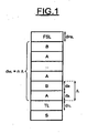
- Figure 1 shows a first embodiment of a component according to the invention, comprising:
- the substrate may consist of a titanium alloy, such as the titanium alloy Ta6V.
- the intermediate layer TL is for example obtained by nitriding the surface of the substrate S.
- the individual layers A and B preferably consist of hydrogenated amorphous silicon carbide, the hydrogenated amorphous silicon carbide of layer A having a lower hardness than that of the hydrogenated amorphous silicon carbide of layer B.
- the functional surface layer consists of an amorphous hydrogenated silicon carbide.
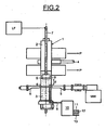
- Figure 2 shows a device for obtaining a component according to the invention, such as that shown in particular in Figure 1 .
- the device comprises a tube reactor 1, of substantially vertical axis.
- a tube reactor of substantially vertical axis.
- Such a reactor is particularly suitable for manufacturing small components.
- the reactor 1 may have a different geometry.
- the reactor 1 is made up of two essential parts, the airlock 2 for loading the specimens and the treatment chamber 3. These parts are separated from each other by a pneumatic slide valve 4 for isolating the chamber 3 when venting the loading airlock 2 for a new load of specimens.
- the loading airlock 2 allows the specimens to be introduced and extracted.
- a horizontal waveguide 5 for example in the form of a silica tube, passes through the treatment chamber 3 in a region 6 where the 2.45 GHz microwave discharge is created.
- This waveguide 5 is connected at one of its ends to a microwave generator MW having a power that varies from 0 tao 1500 W.
- the waveguide 5 conveys, into the treatment zone 3, in the form of surface waves, the energy needed to create and sustain a stable discharge in the treatment chamber 3.
- This stable discharge extends on either side of the zone 6 in which the microwave discharge is created, over a height that depends on a number of parameters, such as the power of the microwave generator MW, the pressure in the treatment chamber, the flow rate of injected gas, etc.
- a discharge may also come from the low-frequency generator LF connected to a transfer tube 7,
- This generator LF makes it possible to apply a range of frequencies from 50 to 400 kHz and a voltage of 0 to 300 V, thereby producing a plasma having other properties.
- This discharge also reaches the zone 6 in which the microwave discharge is created.
- the reactor 1 is equipped with a double pumping system (not shown in Figure 2 ) so as to regulate the pressure within.
- This system consists of a two-stage pumping unit, the output of which is around 240 m 3 /h, making it possible to work with a flux of gas in a primary vacuum during deposition or to pre-evacuate the reactor before switching to a secondary vacuum, and a hybrid turbomolecular unit (250 l/s) (not shown in Figure 2 ) which provides a secondary vacuum with a limit of about 6.5 ⁇ 10 -2 mPa (6.5 ⁇ 10 -7 mbar) so as to limit the contamination of the reactor. It also makes it possible to work with a low gas flux for pressures below 10 Pa (0.1 mbar). These two units are connected both to the loading airlock 2 and to the treatment chamber 3 via electropneumatic valves (not shown in Figure 2 ). These connections are identified by the arrows P.
- the total pressure in the reactor is controlled during the deposition by a throttling valve coupled to a capacitance gauge.
- the motor-operated transfer tube 7 passes right through the entire device, thus making it possible to vary the distance d between the precursor injection pipe 8 and the substrate holder 9.
- the residence time of the species incident on the substrate is defined by the choice of distance d.
- the substrate may be independently heated up to 600°C and is connected, via a tuning box, to the low-frequence generator LF by a capacitive coupling.
- the device illustrated in Figure 2 includes means for injecting various gases into the reactor 1 that are needed for implementing the method and especially for forming the desired thin-film multilayer structure on the substrate S.
- these gas injection means mainly comprise an injection pipe 8 that passes through the bottom of the reactor 1 and runs along the vertical axis of said pipe before emerging in a second region of the treatment chamber 3 located between the substrate S and the zone 6 in which the microwave discharge is created, or in an adjacent part of the zone 6 facing the substrate S.
- the pipe 8 is connected to a flowmeter system 10 for regulating at will the flow rate of the injected gases.
- This flowmeter system 10 is itself connected to an etching gas feed pipe 11, to a pre-treatment gas feed pipe 12 and to a reactive gas or precursor gas feed pipe 13.
- the flowmeter system 10 may be provided with six independent gas lines.
- the etching gas fed via the pipe 11 is advantageously argon and the pre-treatment gas fed via the pipe 12 may be especially hydrogen or nitrogen.
- the reactive or precursor gas fed via the feed pipe 13 is a single organosilicon compound with a silicon tetrahedral environment.
- This compound is preferably tetramethylsilane Si(CH 3 ) 4 (usually denoted by the abbreviation TMS). It is also possible to use tetraethylsilane Si(C 2 H 5 ) 4 (usually denoted by the abbreviation TES) or any other derivative of TMS or TES obtained by substituting one or two ethyl or methyl groups, respectively, with for example hydrogen or chlorine.
- injection pipe 8 may be replaced with any other injection means, such as a system in the form of a ring or grid comprising several injection nozzles, especially if the substrate to be coated is relatively large.
- this other injection means remains in the second region of the treatment chamber 3 defined above and must not obstruct the discharge in which the substrate S is placed.
- the mechanism supporting the substrate holder 9 may have a more complex shape than that illustrated schematically in Figure 2 and may incorporate, for example, at least one motor for moving the substrate holder 9 translationally and/or rotationally. Such arrangements are well known to those skilled in the art and will therefore not be described in further detail.
- vacuum is created, using the two-stage pumping unit for the primary vacuum followed by the second pumping unit for the secondary vacuum.
- Table 1 STEPS OPERATING CONDITIONS Etching - Regulate the working pressure - Inject the etching gases - Turn the microwave and low-frequency generators on - Heat the activated substrate Intermediate layer formation - Regulate the gas for producing the intermediate layer: nitriding Nitriding - Shut off etching gases - Inject the nitriding gases - Apply the bias for nitriding Multilayer deposition preparation - Adjust the gas for depositing the multilayer coatings
- the device described above by means of Figure 2 was used to manufacture a component that includes a multilayer structure according to the invention.
- the deposition procedure as defined in Table 1 above was applied so as to treat the surface of a substrate made of a TA6V titanium alloy.
- the particular temperature, pressure, gas flow rate and voltage conditions used are given in Table 2 below.
- a component was obtained that comprised:
Landscapes
- Chemical & Material Sciences (AREA)
- Engineering & Computer Science (AREA)
- Materials Engineering (AREA)
- General Chemical & Material Sciences (AREA)
- Chemical Kinetics & Catalysis (AREA)
- Mechanical Engineering (AREA)
- Metallurgy (AREA)
- Organic Chemistry (AREA)
- Plasma & Fusion (AREA)
- Physics & Mathematics (AREA)
- Inorganic Chemistry (AREA)
- Chemical Vapour Deposition (AREA)
- Other Surface Treatments For Metallic Materials (AREA)
Description
- The present invention relates to a corrosion-resistant thin-film multilayer structure having a low wear rate and a low coefficient of friction, to a component comprising said structure and to its method of deposition.
- For some ten years, hard films with a low wear rate, more particularly those with a low wear rate and a low coefficient of friction, have offered considerable advantages in many thermomechanical fields of application, such as cutting tools, mechanical components, rolling members and gears. For example, there is currently a growing interest in producing such films on metal alloys, such as titanium alloys for the aeronautical or aerospace industry.
- The thin films are generally produced by PVD (physical vapour deposition). In particular, when the thin films are intended to be subjected to frictional wear, they may be based on a nitride and/or a carbide, for example TiN, TiCN, TiCrN, CrC or TiAlN, and are produced by PVD on a titanium-based substrate, or they may be of the adamantine carbon or DLC (diamond-like carbon) type, that is to say of the type consisting of hydrogenated or unhydrogenated amorphous carbon, which are produced by PACVD (plasma-assisted chemical vapour deposition).
- The term DLC covers a wide variety of lightly or highly hydrogenated materials. They are customarily used in applications requiring a high hardness and a high elastic modulus, for example 15-30 GPa and 200-280 GPa respectively. This gives them, under the conditions of use, low coefficients of friction (µ) and limited wear rates of the order of 10-6-10-7 mm3.N.m-1. The coefficient of friction is less than 0.2, especially with respect to steels, aluminium alloys and titanium alloys. For the latter two alloy, such a low level of friction is exceptional. The demand for this type of coating in the engineering industry is therefore becoming greater and greater as one of the main properties of DLC coatings is abrasive wear resistance, which is much higher than for nitride-type materials of equivalent hardness, owing to their high elastic modulus.
- However, they have the drawback of limited corrosion resistance:
- (i) in a dry medium, DLCs oxidize above 400°C, resulting in degradation (graphitization) above about 400°C; and
- (ii) in a wet medium, growth defects induce pitting corrosion.
- In addition, DLCs are highly strained, which requires complex sublayers for matching the strain or elastic modulus profiles between the coated component and the upper layer. The presence of these accommodating layers or sublayers, which have various thicknesses ranging up to a few microns, makes it difficult to predict the mechanical properties associated with the adhesion of the films to the substrates, the mechanical strength under load, the physico-chemical interaction of the various superposed materials, and the thermal resistance of the whole assembly. These multilayer systems induce an additional degree of difficulty as regards optimizing the behaviour of the coating for the desired function.
-
Patent Application FR 2 736 361
however, the coatings of the prior art do not satisfy the industrial requirements of coatings for tribological purposes (limiting the wear and friction, as explained in the prior art) on metal substrates. - There is therefore a need for a coating having, simultaneously:
- tribological properties, such as a low wear rate and a low coefficient of friction when dry (i.e. without the addition of a lubricant moreover) with respect to metal surfaces in a corrosive atmosphere and/or at high temperature;
- - adhesion properties, such as a high mechanical strength of the coating on metal substrates; and
- - a high resistance of the coatings at high temperature, for example above 400°C, without modifying the tribological properties of the coatings and adhesion to their substrates.
- The Applicant has found, surprisingly, that one particular multilayer structure provides such a combination of properties by associating several layers based on silicon, carbon and hydrogen, with a thickness ranging from 5 nm to 5 µm, which have different tribological properties, at least two layers forming a period, each period being repeated n times where n ranges from 1 to 1000.
- One subject of the invention is therefore the corrosion-resistant thin-film multilayer structure having a low wear rate and a low coefficient of friction defined in claim 1.
- The expression "low coefficient of friction" is understood within the present invention to mean a coefficient of friction µ of less than 0.2, for example:
- under the conditions for tribological tests carried out using a rotary tribometer, under an applied normal load of 3 N, for a travel distance of 100 m and a speed of displacement of 0.02 m.s-1, running dry, i.e. without addition of lubricant moreover, in a 25°C ambient laboratory atmosphere, and with an opposing metal body consisting of a
ball 6 mm in diameter made of 100C6 steel; and - under reciprocating friction test conditions, with a to-and-fro movement, under an applied normal load of 3 N, for a travel distance of 20 m and a speed of displacement of 0.00017 m.s-1, running dry, that is to say without the addition of lubricant moreover, in a 25°C ambient laboratory atmosphere, and with an opposing metal body consisting of a
ball 6 mm in diameter made of 100C6 steel. - A low coefficient of friction makes it possible to envisage using said structure in many industrial fields, whenever contacting components are required to move one relative to the other, either continuously or intermittently.
- The expression "low wear rate" is understood within the context of the present invention to mean a wear rate of less than 10-5 mm3.N.m-1 measured under the tribological test conditions described above, by profilometry of the wear tracks after rubbing the films.
- The term "corrosion resistance" is understood within the present invention to mean a dissolution potential that reaches the dissolution potential of the substrate after 100 hours, measured electrochemically in an aqueous 5% NaCl solution at a pH of 5.5 at a temperature of 25°C, with a saturated calomel reference electrode.
- The multilayer structure preferably has a total thickness of 10 µm or less, preferably from 1 to 6 µm.
- Each layer in the period consists of carbon, silicon and hydrogen, the Si/C atomic ratio ranging in particular from 0.3 to 1.5. The proportion of hydrogen preferably varies from 10 to 30 at%.
- The thickness of each layer in the period is preferably within the range from 5 nm to 5 µm, better still from 10 mm to 1 µm and even more preferably from 10 nm to 500 nm.
- Each layer has, independently of one another in a period, specific mechanical properties, which are the same or different, such as a hardness of 1 to 100 GPa, preferably 5 to 80 GPa, and a Young's elastic modulus of 10 to 600 GPa, preferably 80 to 400 GPA. These physical properties are measured by the nanoindentation technique, with a Berkovich indenter and under loads between 0.5 mN and 200 mN, allowing penetration depths of 10 nm to 1.5 µm to be achieved.
- The adhesion properties are measured by the scratch resistance test. The test conditions are the following: a Rockwell diamond stylus of spherical geometry with a radius of 200 µm is applied to the surface of the thin film with a gradually increasing normal load varying from 0 to 30 N with a constant speed of 5 mm/min over a distance of 5 mm. Good adhesion corresponds to a critical load (Lc2) of greater than 15 N, preferably greater than 20 N.
- The term "functional layer" is understood within the context of the present invention to mean a layer exhibiting remarkable corrosion resistance properties, scratch resistance properties or tribological properties such as, for example, a low coefficient of friction and a low wear rate.
- The optional functional surface layer imparts properties different from those of the layers of the periods lying beneath it.
- The functional layer essentially comprises carbon, i.e. 30 to 100 at%, preferably 40 to 90 at%, carbon. It may also comprise additional elements such as silicon, hydrogen, sulphur, fluorine, titanium or tungsten, these additional elements being preferably present in a proportion of 0 to 70 at%, better still 10 to 60 at%.
- The thickness of the latter layer preferably does not exceed 3 µm and more particularly lies in the range from 1 nm to 2 µm.
- This functional surface layer also has mechanical properties such as a hardness of 1 to 100 GPa, preferably 5 to 80 GPa, and a Young' s modulus of 10 to 600 GPa, preferably 80 to 400 GPa.
- The subject of the invention is also a corrosion-resistant component having a low wear rate and a low coefficient of friction, comprising:
- a metal substrate made of a material that is not impaired when it is heated to a temperature below 600 °C, preferably in a range from 200 to 600°C;
- a tie layer; and
- a surface coating covering said tie layer, the surface coating being a thin-film multilayer structure according to the invention as defined above.
- The metal substrate is preferably made of titanium or one of its alloys, such as TA6V or Ti10.2.3, high-speed steel, such as steels HS18-0-1 and HS6-5-2-5, stainless steel, or a carbide such as WC + Co K10 and WC + TiC + Ta (Nb) C + Co P 10
K 10. - The tie layer interposed between the substrate and the surface coating is nitrided, carburized, carbonitrided or silicided preferably nitrided. As an example of a nitride, mention may in particular be made of titanium nitride when the substrate is based on titanium.
- Said tie layer may be produced from an argon/hydrogen/nitrogen mixture, which also allows the surface of the metal substrate to be functionalized so as in particular to promote adhesion of the multilayer structure to the substrate, while limiting its deformation when subjected to a load. The surface nitrogen concentration is preferably in the range from 20 at% to 80 at%.
- The thickness of the tie layer is preferably in the range from 0.1 µm to 100 µm, better still from 0.2 µm to 10 µm.
- This component has the advantage of combining the following properties:
- the coatings possess good tribological properties, that is to say without a lubricant, with a low wear rate and a low coefficient of friction with respect to metal surfaces in an ambient and/or corrosive and/or high-temperature atmosphere;
- the coatings exhibit good temperature resistance without their adhesion and tribological properties being modified, for example a low wear rate and a low coefficient of friction, in particular up to 550°C, and are corrosion-resistant;
- the complex architecture, consisting of multilayers, allows the mechanical cracking resistance behaviour of the system to be improved; and
- the optional tie layer, essentially consisting of nitrogen and hydrogen, furthermore allows the surface of the metal substrate to be functionalized, while limiting its deformation when subjected to a load.
- The invention also relates to a method of depositing a surface coating in the form of a corrosion-resistant thin-film multilayer structure having a low wear rate and a low coefficient of friction on a metal substrate made of a material that is not impaired when it is heated to a temperature below 600°C, by chemical vapour deposition, activated by a microwave plasma and /or by a low-frequency plasma, comprising the following successive steps:
- i) installation of the substrate on a support, in a chamber comprising an introduction/extraction zone (called an airlock) and an active zone that can contain a plasma of maximum density, this installation step being followed by the following surface treatment step:
- ii) creation of a primary vacuum inside the chamber followed by a secondary vacuum;
- iii) etching of the substrate in the active zone by injecting an etching gas in a primary vacuum, creation of a plasma of this gas in a discharge zone (contained in the active zone) and by separately heating the substrate to a regulated temperature between 200°C and 600°C;
- iv) formation of a tie layer as described above by injecting a pre-treatment gas into the active zone of the chamber, so as to substitute the etching gas plasma with a pre-treatment gas plasma, while continuing to heat the substrate at said regulated temperature;
- v) formation of the multilayer structure as described above by injecting a reactive gas into the active zone, this reactive gas comprising a single compound having a tetrahedral silicon environment or a silicon-containing mixture, so as to substitute the pre-treatment gas plasma with a reactive gas, while continuing to heat the substrate at said regulated temperature, the various layers being obtained by modifying the power of the microwave generator and/or the frequency and/or the voltage of the low-frequency generator;
- vi) optional deposition of the functional surface layer in the active zone, by injecting another reactive gas, so as to substitute the plasma of the gas for producing the multilayer structure with a plasma of the reactive gas, while continuing to heat at said regulated temperature; and
- vii) interruption of the reactive gas injection of step v) or step vi) and cooling of the substrate, after a predetermined injection time corresponding to the desired thickness of the functional surface layer, the primary vacuum created inside the chamber corresponding to a pressure of 0.13 to 133.3 Pa (10-3 to 1 torr), preferably 0.13 to 66.7 Pa (10-3 to 0.5 torr), and better still 0.13 to 13.3 Pa (10-3 to 10-1 torr).
- The secondary vacuum may be, for instance, around 6.5 × 10⁻² mPa (6.5 × 10⁻⁷ mbar) and allows the atmosphere within the zone to be purified.
- The gas injected into the active zone may especially be excited by a discharge coming from a microwave source connected to a microwave generator that works at a frequency of 2.45 GHz or 915 MHz, the power of the generator being set between 0 W and 1500 W, and/or coming from a low-frequency generator, the frequency of which ranges from 50 to 460 kHz and the voltage from 0 to 300 V, and the surface power density of which is of the order of 10 w/cm2, in order to obtain a gas plasma.
- By modifying the power of the microwave generator and/or especially the voltage of the low-frequency generator, it is possible to obtain layers based on C, Si and H using one and the same reactive gas, having different tribological properties.
- The etching gas used in step iii) is advantageously argon, to which hydrogen may be added, and its injection rate while etching the substrate is preferably between 0.1 Sl/h (standard litres per hour) and 10 Sl/h.
- The pre-treatment gas used in step iv) contains the element nitrogen and/or the element carbon and/or the element hydrogen and/or the element silicon. Examples of such elements may especially be nitrogen, methane, ethane, acetylene, ethylene, hydrogen, silane and disilane, and mixtures thereof. In a preferred implementation of the method, the pre-treatment gas comprises at most about 20% nitrogen and/or methane and/or silane and/or hydrogen, mixed with argon.
- It is important to note that the etching may be carried out and the tie layer may be produced in the chamber used for depositing the coating, practically without interruption.
- Advantageously, the reactive gas used in step v) comprises tetramethylsilane (TMS) or tetraethylsilane (TES) by itself or as a mixture, or else a mixture of precursors of hydrocarbons, such as methane, ethane, acetylene or ethylene, and/or of silicon-containing compounds, such as silane or disilane.
- The reactive gas of this step v) may furthermore contain argon and/or hydrogen. Its injection rate is preferably less than 2 Sl/h.
- Preferred embodiments of the invention will now be described by way of non-limiting illustration, with reference to the example and to the appended drawings in which:
-
Figure 1 is a schematic view of one embodiment of a component comprising a multilayer structure according to the invention; and -
Figure 2 is a schematic view of a device, of the PACVD deposition reactor type, for implementing the method according to the invention. -
Figure 1 shows a first embodiment of a component according to the invention, comprising: - a metal substrate S;
- a tie layer TL, having a thickness dTL;
- n periods, each period comprising two individual layers A and B with respective thicknesses of dA and dB, the thickness of a period A thus being equal to the sum of the individual thicknesses dA and dB: Λ = dA + dB, and the thickness of the multilayer dML being equal to nA; and
- a functional surface layer FSL of thickness DFSL, consisting of a hydrogenated carbide, said carbide satisfying for example the formula XC, where X denotes an addition element such as S, Si, W, Ti or F.
- The substrate may consist of a titanium alloy, such as the titanium alloy Ta6V.
- The intermediate layer TL is for example obtained by nitriding the surface of the substrate S.
- The individual layers A and B preferably consist of hydrogenated amorphous silicon carbide, the hydrogenated amorphous silicon carbide of layer A having a lower hardness than that of the hydrogenated amorphous silicon carbide of layer B.
- As an example, the functional surface layer consists of an amorphous hydrogenated silicon carbide.
-
Figure 2 shows a device for obtaining a component according to the invention, such as that shown in particular inFigure 1 . - The device comprises a tube reactor 1, of substantially vertical axis. Such a reactor is particularly suitable for manufacturing small components. For more voluminous components, the reactor 1 may have a different geometry.
- The reactor 1 is made up of two essential parts, the
airlock 2 for loading the specimens and thetreatment chamber 3. These parts are separated from each other by a pneumatic slide valve 4 for isolating thechamber 3 when venting theloading airlock 2 for a new load of specimens. - The
loading airlock 2 allows the specimens to be introduced and extracted. - A
horizontal waveguide 5, for example in the form of a silica tube, passes through thetreatment chamber 3 in aregion 6 where the 2.45 GHz microwave discharge is created. Thiswaveguide 5 is connected at one of its ends to a microwave generator MW having a power that varies from 0 tao 1500 W. - The
waveguide 5 conveys, into thetreatment zone 3, in the form of surface waves, the energy needed to create and sustain a stable discharge in thetreatment chamber 3. - This stable discharge extends on either side of the
zone 6 in which the microwave discharge is created, over a height that depends on a number of parameters, such as the power of the microwave generator MW, the pressure in the treatment chamber, the flow rate of injected gas, etc. - A discharge may also come from the low-frequency generator LF connected to a
transfer tube 7, This generator LF makes it possible to apply a range of frequencies from 50 to 400 kHz and a voltage of 0 to 300 V, thereby producing a plasma having other properties. - This discharge also reaches the
zone 6 in which the microwave discharge is created. - This or these stable discharges make it possible to sustain a gas plasma, the extent of which is depicted in
Figure 2 by a grey zone. - The reactor 1 is equipped with a double pumping system (not shown in
Figure 2 ) so as to regulate the pressure within. This system consists of a two-stage pumping unit, the output of which is around 240 m3/h, making it possible to work with a flux of gas in a primary vacuum during deposition or to pre-evacuate the reactor before switching to a secondary vacuum, and a hybrid turbomolecular unit (250 l/s) (not shown inFigure 2 ) which provides a secondary vacuum with a limit of about 6.5 × 10⁻² mPa (6.5 × 10⁻⁷ mbar) so as to limit the contamination of the reactor. It also makes it possible to work with a low gas flux for pressures below 10 Pa (0.1 mbar). These two units are connected both to theloading airlock 2 and to thetreatment chamber 3 via electropneumatic valves (not shown inFigure 2 ). These connections are identified by the arrows P. - The total pressure in the reactor is controlled during the deposition by a throttling valve coupled to a capacitance gauge.
- The motor-operated
transfer tube 7 passes right through the entire device, thus making it possible to vary the distance d between theprecursor injection pipe 8 and thesubstrate holder 9. The residence time of the species incident on the substrate is defined by the choice of distance d. The substrate may be independently heated up to 600°C and is connected, via a tuning box, to the low-frequence generator LF by a capacitive coupling. - In addition to the various component parts that have just been described, the device illustrated in
Figure 2 includes means for injecting various gases into the reactor 1 that are needed for implementing the method and especially for forming the desired thin-film multilayer structure on the substrate S. - In the embodiment shown, these gas injection means mainly comprise an
injection pipe 8 that passes through the bottom of the reactor 1 and runs along the vertical axis of said pipe before emerging in a second region of thetreatment chamber 3 located between the substrate S and thezone 6 in which the microwave discharge is created, or in an adjacent part of thezone 6 facing the substrate S. Outside the reactor 1, thepipe 8 is connected to aflowmeter system 10 for regulating at will the flow rate of the injected gases. Thisflowmeter system 10 is itself connected to an etchinggas feed pipe 11, to a pre-treatmentgas feed pipe 12 and to a reactive gas or precursorgas feed pipe 13. - In an alternative embodiment, the
flowmeter system 10 may be provided with six independent gas lines. - The etching gas fed via the
pipe 11 is advantageously argon and the pre-treatment gas fed via thepipe 12 may be especially hydrogen or nitrogen. - The reactive or precursor gas fed via the
feed pipe 13 is a single organosilicon compound with a silicon tetrahedral environment. This compound is preferably tetramethylsilane Si(CH3)4 (usually denoted by the abbreviation TMS). It is also possible to use tetraethylsilane Si(C2H5)4 (usually denoted by the abbreviation TES) or any other derivative of TMS or TES obtained by substituting one or two ethyl or methyl groups, respectively, with for example hydrogen or chlorine. - It should be noted that the
injection pipe 8 may be replaced with any other injection means, such as a system in the form of a ring or grid comprising several injection nozzles, especially if the substrate to be coated is relatively large. However, this other injection means remains in the second region of thetreatment chamber 3 defined above and must not obstruct the discharge in which the substrate S is placed. - Moreover, when the substrate to be coated is relatively large, it may also be necessary for there to be relative movement between the reactive gas injection system, such as the
injection pipe 8, and thesubstrate holder 9. For this purpose, the mechanism supporting thesubstrate holder 9 may have a more complex shape than that illustrated schematically inFigure 2 and may incorporate, for example, at least one motor for moving thesubstrate holder 9 translationally and/or rotationally. Such arrangements are well known to those skilled in the art and will therefore not be described in further detail. - As soon as the substrate or substrates S are positioned on the
substrate holder 9 in the reactor 1, vacuum is created, using the two-stage pumping unit for the primary vacuum followed by the second pumping unit for the secondary vacuum. - After positioning the specimens, a deposition procedure described in Table 1 below is applied.
Table 1 STEPS OPERATING CONDITIONS Etching - Regulate the working pressure - Inject the etching gases - Turn the microwave and low-frequency generators on - Heat the activated substrate Intermediate layer formation - Regulate the gas for producing the intermediate layer: nitriding Nitriding - Shut off etching gases - Inject the nitriding gases - Apply the bias for nitriding Multilayer deposition preparation - Adjust the gas for depositing the multilayer coatings Periodic multilayer deposition: 10 periods 1st layer of period 1: - apply deposition power and bias 1 - inject deposition gas 1 2nd layer of period 1: - apply deposition power and bias 2 - inject deposition gas 21st layer of period 2: - apply deposition power and bias 1 - inject deposition gas 1 2nd layer of period 2: - apply deposition power and bias 2 - inject deposition gas 2...... 1st layer of period 10: - apply deposition power and bias 1 - inject deposition gas 1 2nd layer of period 10: - apply deposition power and bias 2 - inject deposition gas 2Surface layer deposition preparation - Adjust the gas for producing the surface coating Deposition of the surface layer - Apply deposition power and bias for the functional surface - Inject the gases Cooling phase - Turn off the microwave and low-frequency generators - Stop injecting the gases - Stop heating the substrate - The device described above by means of
Figure 2 was used to manufacture a component that includes a multilayer structure according to the invention. To do this, the deposition procedure as defined in Table 1 above was applied so as to treat the surface of a substrate made of a TA6V titanium alloy. The particular temperature, pressure, gas flow rate and voltage conditions used are given in Table 2 below.Table 2 Step Operating conditions Objective Etching P = 0.1 torr
Flow (Ar)1 = 7%
Vdc = -100 V
Power = 500 WTo regulate the working pressure
To ignite the Ar plasma To biasHeating: 540°C To reach T = 540°C Flow (Ar)2 = 7.3%
Flow (N2) = 11%To prepare the nitriding flows to ROOTS Cut Vdc To stop the bias Nitriding Power = 500 W To inject the Ar/N2 mixture Nitriding gas purge and deposition line preparation N2 inlet closed
Flow (TMS) = 35%
Flow (Ar)2 = 1%To purge N2 from the chamber and prepare the flows for the deposition phase
To prepare the bias during depositionPower = 700 W To reach the deposition power Multilayer + functional layer deposition LF generator off
P = 700 WTo inject the gases into the chamber for depositing a layer with no bias LF generator on
Vdc = -100 V
P = 700 WTo inject the gases into the chamber for depositing a layer with bias ... ... LF generator off P = 700 W To inject the gases into the chamber for depositing a layer with no bias Cooling Flow (Ar)1 To extinguish the plasma To shut off the gases To stop heating To cool in argon - A component was obtained that comprised:
- a plasma-etched TA6V titanium alloy substrate;
- a nitride tie layer;
- a complex multilayer according to the invention comprising 10 periods, each period comprising 2 layers each 140 nm in thickness; and
- a functional surface layer.
- The component obtained may be represented by the diagram in
Figure 1 , in which: - thickness of the tie layer: dTL = 700 nm;
- thicknesses of the individual layers of the multilayer: dA = 140 nm and dB = 140 nm;
- thickness of the period: A = dA + dB = 140 + 140 = 280 nm;
- number of periods: n = 10, resulting in a total multilayer thickness dML = nΛ = 10×280 = 2800 nm; and
- thickness of the carbon-based functional surface layer: dFSL = 200 nm.
- The composition and the properties of the various layers of the component are given in Tables 3 and 4 below.
Table 3 Composition Hydrogen
(at%)Atomic composition Thickness
(nm)Hardness (GPa) Young's modulus
(GPa)Tie layer
(TL)Nitrogen - N = 54 at% 700 19.1 211 Soft a-SiC:H
1st layer
(A) of the periodCarbon, Silicon, Hydrogen 20 Si/C = 0.59 140 20.4 141 Hard a-SiC:H
2nd layer
(B) of the periodCarbon, Silicon, Hydrogen 20 Si/C = 0.59 140 24.1 153 Functional surface layer (FSL) Carbon, Silicon, Hydrogen 20 Si/C = 0.60 200 20.4 141 - The mechanical properties of the specimen obtained above, such as the wear rates and the coefficient of friction, and also the corrosion resistance and the adhesion, were then measured. The results are given in Table 4 below.
Table 4: properties of the multilayer structure Properties Tests Results Mechanical Rotary friction Friction µ = 0.06 Wear < 10-5 mm3.N.m-1 Reciprocating friction Friction µ = 0.15 Wear < 10-5 mm3.N.m-1 Corrosion Electrochemical Dissolution potential 100 hours Adhesion Scratch resistance Critical threshold load for adhesive failure = 22.5 N
Claims (19)
- Corrosion-resistant thin-film multilayer structure having a low wear rate and a low coefficient of friction, characterized in that it comprises:• 1 to 1000 periods, preferably 1 to 500 periods, one period comprising 2 to 100 layers (A, B) , preferably 2 to 10 layers,
each layer (A, B) in the period consisting of carbon, silicon and hydrogen, and containing 10 to 30 at% hydrogen, the Si/C atomic ratio ranging from 0.3 to 1.5, and• optionally, a functional surface layer (FSL). - Thin-film multilayer structure according to Claim 1, characterized in that it has a total thickness of 10 µm or less.
- Thin-film multilayer structure according to Claim 2, characterized in that it has a total thickness ranging from 1 to 6 µm.
- Thin-film multilayer structure according to any one of the preceding claims, characterized in that the thickness (dA, dB) of each layer varies from 5 nm to 5 µm.
- Thin-film multilayer structure according to any one of the preceding claims, characterized in that each layer (A, B) in the period has, independently of one another in a period, a hardness of 1 to 100 GPa and a Young's modulus of 10 to 600 GPa.
- Thin-film multilayer structure according to any one of the preceding claims, characterized in that the functional surface layer (FSL) essentially comprises carbon.
- Thin-film multilayer structure according to Claim 6, characterized in that the functional surface layer (FSL) contains 30 to 100 at% carbon.
- Thin-film multilayer structure according to Claim 6 or 7, characterized in that the functional surface layer (FSL) comprises additional elements chosen from silicon, hydrogen, sulphur, fluorine, titanium and tungsten, in proportions ranging from 0 to 70 at%.
- Thin-film multilayer structure according to any one of the preceding claims, characterized in that the thickness (dFSL) of the functional surface layer is 3 µm or less.
- Thin-film multilayer structure according to Claim 9, characterized in that the thickness (DFSL) of the functional surface layer lies in the range from 1 nm to 2 µm.
- Corrosion-resistant component having a low wear rate and a low coefficient of friction, characterized in that it comprises:- a metal substrate made of a material that is not impaired when it is heated to a temperature ranging up to 600°C;- a tie layer interposed between the substrate and the surface coating; and- a surface coating covering the tie layer, the surface coating being a thin-film multilayer structure according to any one of Claims 1 to 10.
- Component according to Claim 11, characterized in that the metal substrate is made of titanium or one of its alloys, high-speed steel, stainless steel, or a carbide.
- Component according to Claim 11 or 12, characterized in that the tie layer is nitrided, carburized, carbonitrided or silicided.
- Component according to any one of Claims 11 to 13, characterized in that the tie layer has a thickness of 0.1 to 100 µm.
- Method of depositing a surface coating in the form of a corrosion-resistant thin-film multilayer structure having a low wear rate and a low coefficient of friction on a metal substrate made of a material that is not impaired when it is heated to a temperature below 600°C, by chemical vapour deposition, activated by a microwave plasma and/or by a low-frequency plasma, comprising the following successive steps:i) installation of the substrate on a support, in a chamber comprising an introduction/extraction zone and an active zone that can contain a plasma of maximum density, this installation step being followed by the following surface treatment steps:ii) creation of a primary vacuum inside the chamber followed by a secondary vacuum;iii) etching of the substrate in the active zone by injecting an etching gas in a primary vacuum, creation of a plasma of this gas in a discharge zone and by separately heating the substrate to a regulated temperature between 200°C and 600°C;iv) formation of a tie layer by injecting a pretreatment gas into the active zone of the chamber, so as to substitute the etching gas plasma with a pre-treatment gas plasma, while continuing to heat the substrate at said regulated temperature;v) formation of the multilayer structure according to any one of Claims 1 to 10 by injecting a reactive gas into the active zone, this reactive gas comprising a single compound having a tetrahedral silicon environment or a silicon-containing mixture, so as to substitute the pre-treatment gas plasma with a reactive gas, while continuing to heat the substrate at said regulated temperature, the various layers being obtained by modifying the power of the microwave generator and/or the frequency and/or the voltage of the low-frequency generator;vi) optional deposition of the functional surface layer in the active zone, by injecting another reactive gas, so as to substitute the plasma of the gas for producing the multilayer structure with a plasma of the reactive gas, while continuing to heat at said regulated temperature; andvii) interruption of the reactive gas injection of step v) or step vi) and cooling of the substrate, after a predetermined injection time corresponding to the desired thickness of the functional surface layer, the primary vacuum created inside the chamber corresponding to a pressure of 0.13 to 133.3 Pa (10-3 to 1 torr), preferably 0.13 to 66.7 Pa (10-3 to 0.5 torr).
- Method according to Claim 15, characterized in that the pre-treatment gas contains the element nitrogen and/or the element carbon and/or the element hydrogen and/or the element silicon.
- Method according to Claim 16, characterized in that the pre-treatment gas comprises at most about 20% nitrogen and/or methane, mixed with argon.
- Method according to any one of Claims 15 to 17, characterized in that the reactive gas of step v) comprises tetramethylsilane (TMS) or tetraethylsilane (TES) by itself or as a mixture, or else a mixture of precursors of hydrocarbons and/or of silicon-containing compounds.
- Method according to Claim 18, characterized in that the reactive gas also contains hydrogen and/or argon.
Applications Claiming Priority (2)
| Application Number | Priority Date | Filing Date | Title |
|---|---|---|---|
| FR0600829A FR2896807B1 (en) | 2006-01-30 | 2006-01-30 | THIN MULTILAYER STRUCTURE, PIECE COMPRISING SAME AND ITS DEPOSITION METHOD |
| PCT/EP2007/000779 WO2007085494A1 (en) | 2006-01-30 | 2007-01-30 | Thin-film multilayer structure, component comprising said structure and its method of deposition |
Publications (2)
| Publication Number | Publication Date |
|---|---|
| EP1979505A1 EP1979505A1 (en) | 2008-10-15 |
| EP1979505B1 true EP1979505B1 (en) | 2010-05-19 |
Family
ID=36954446
Family Applications (1)
| Application Number | Title | Priority Date | Filing Date |
|---|---|---|---|
| EP07703133A Not-in-force EP1979505B1 (en) | 2006-01-30 | 2007-01-30 | Thin-film multilayer structure, component comprising said structure and its method of deposition |
Country Status (9)
| Country | Link |
|---|---|
| US (1) | US20090081433A1 (en) |
| EP (1) | EP1979505B1 (en) |
| JP (1) | JP2009525397A (en) |
| CN (1) | CN101360845A (en) |
| DE (1) | DE602007006626D1 (en) |
| ES (1) | ES2345910T3 (en) |
| FR (1) | FR2896807B1 (en) |
| RU (1) | RU2418883C2 (en) |
| WO (1) | WO2007085494A1 (en) |
Families Citing this family (6)
| Publication number | Priority date | Publication date | Assignee | Title |
|---|---|---|---|---|
| CN101736325B (en) * | 2010-01-05 | 2012-07-04 | 青岛科技大学 | Microwave plasma preparation method of superhard titanium aluminum nitride thin film |
| CN102358940B (en) * | 2011-10-12 | 2014-06-04 | 湖北久之洋红外系统股份有限公司 | Method for depositing anti-corrosion diamond-like film on object substrate |
| US9988706B2 (en) * | 2012-05-03 | 2018-06-05 | Magna International Inc. | Automotive components formed of sheet metal coated with a non-metallic coating |
| DE102013109646B4 (en) | 2013-09-04 | 2021-12-02 | Pictiva Displays International Limited | Organic optoelectronic component |
| US10418243B2 (en) * | 2015-10-09 | 2019-09-17 | Applied Materials, Inc. | Ultra-high modulus and etch selectivity boron-carbon hardmask films |
| FR3075231B1 (en) * | 2017-12-18 | 2019-11-15 | Compagnie Generale Des Etablissements Michelin | SOIL AND DEVICE AND ASSOCIATED METHODS |
Family Cites Families (10)
| Publication number | Priority date | Publication date | Assignee | Title |
|---|---|---|---|---|
| JPS6067901A (en) * | 1983-09-24 | 1985-04-18 | Agency Of Ind Science & Technol | Optical element using thin film of hydrogenated and fluorinated amorphous silicon carbide |
| JPS60184681A (en) * | 1984-03-02 | 1985-09-20 | Sharp Corp | Amorphous silicon carbide film for coating |
| US5122431A (en) * | 1988-09-14 | 1992-06-16 | Fujitsu Limited | Thin film formation apparatus |
| JP2761253B2 (en) * | 1989-08-11 | 1998-06-04 | シャープ株式会社 | Optical writing type liquid crystal display |
| US5249554A (en) * | 1993-01-08 | 1993-10-05 | Ford Motor Company | Powertrain component with adherent film having a graded composition |
| RU2089664C1 (en) * | 1994-06-02 | 1997-09-10 | Анатолий Адамович Уэльский | Method of applying multilayer metal coating to restore worn parts and its modification |
| FR2736361B1 (en) * | 1995-07-03 | 1997-09-19 | Aerospatiale | COMPLEX THIN LAYER, PIECE WITH LOW COEFFICIENT OF FRICTION COATED WITH SUCH A LAYER AND METHOD FOR PRODUCING SUCH A PIECE |
| RU2192504C1 (en) * | 2001-04-23 | 2002-11-10 | Московский государственный институт стали и сплавов (технологический университет) | Device for deposition of protective coatings on small-size articles |
| FR2856078B1 (en) * | 2003-06-16 | 2006-11-17 | Commissariat Energie Atomique | COATING FOR A MECHANICAL PART COMPRISING AT LEAST HYDROGENATED AMORPHOUS CARBON AND METHOD OF DEPOSITING SUCH COATING. |
| JP2005076099A (en) * | 2003-09-02 | 2005-03-24 | Konica Minolta Holdings Inc | Method of producing thin film, thin film produced thereby, stacked thin film, transparent plastic film, and organic el element with stacked thin film |
-
2006
- 2006-01-30 FR FR0600829A patent/FR2896807B1/en not_active Expired - Fee Related
-
2007
- 2007-01-30 DE DE602007006626T patent/DE602007006626D1/en active Active
- 2007-01-30 JP JP2008551733A patent/JP2009525397A/en active Pending
- 2007-01-30 ES ES07703133T patent/ES2345910T3/en active Active
- 2007-01-30 CN CNA2007800014638A patent/CN101360845A/en active Pending
- 2007-01-30 RU RU2008135371/02A patent/RU2418883C2/en not_active IP Right Cessation
- 2007-01-30 WO PCT/EP2007/000779 patent/WO2007085494A1/en not_active Ceased
- 2007-01-30 US US12/162,377 patent/US20090081433A1/en not_active Abandoned
- 2007-01-30 EP EP07703133A patent/EP1979505B1/en not_active Not-in-force
Also Published As
| Publication number | Publication date |
|---|---|
| CN101360845A (en) | 2009-02-04 |
| DE602007006626D1 (en) | 2010-07-01 |
| ES2345910T3 (en) | 2010-10-05 |
| RU2008135371A (en) | 2010-03-10 |
| RU2418883C2 (en) | 2011-05-20 |
| US20090081433A1 (en) | 2009-03-26 |
| JP2009525397A (en) | 2009-07-09 |
| FR2896807A1 (en) | 2007-08-03 |
| WO2007085494A1 (en) | 2007-08-02 |
| EP1979505A1 (en) | 2008-10-15 |
| FR2896807B1 (en) | 2008-03-14 |
Similar Documents
| Publication | Publication Date | Title |
|---|---|---|
| Sánchez-López et al. | Doping and alloying effects on DLC coatings | |
| Al Mahmud et al. | An updated overview of diamond-like carbon coating in tribology | |
| Ferreira et al. | Diamond-like carbon coatings deposited by deep oscillation magnetron sputtering in Ar-Ne discharges | |
| KR100404006B1 (en) | Amorphous hard carbon film, mechanical parts and method for producing amorphous hard carbon film | |
| Chang et al. | Microstructure and adhesion characteristics of diamond-like carbon films deposited on steel substrates | |
| JP7857924B2 (en) | Hard carbon coating with improved adhesive strength by HiPIMS and method thereof | |
| US20110162751A1 (en) | Protective Coatings for Petrochemical and Chemical Industry Equipment and Devices | |
| US20120270064A1 (en) | Slide member including diamond-like-carbon film | |
| US20090081433A1 (en) | Thin-film multilayer structure, component comprising said structure and its method of deposition | |
| Wu et al. | Friction and wear properties of CrSiCN coatings with low carbon content as sliding against SiC and steel balls in water | |
| CN1289861A (en) | Preparation method of diamond-like carbon film deposited by cathodic arc evaporation | |
| Bi et al. | Effect of Si/O doping on the thermal stability of non-bonded hydrogenated diamondlike carbon coatings | |
| Wang et al. | The effect of acetylene flow rate on the uniform deposition of thick DLC coatings on the inner surface of pipes with different draw ratios | |
| Wu et al. | Microstructure, mechanical and tribological properties of CrSiC coatings sliding against SiC and Al2O3 balls in water | |
| Nishimoto et al. | Duplex treatment of active screen plasma nitriding and amorphous hydrogenated carbon coating | |
| Zuo et al. | A study on the mechanical performance and medium temperature tribological behavior of plasma nitrocarburizing/TiAlSiN/DLC composite coating | |
| Mei et al. | Influence of Ar/C2H2 flow ratio on the microstructure and properties of Cr-containing DLC films deposited by medium frequency magnetron sputtering | |
| Mou et al. | Diamond and diamond-like carbon for tribology and corrosion protection: a retrospective review | |
| Jedrzejczak et al. | Titanium (IV) isopropoxide as a source of titanium and oxygen atoms in carbon based coatings deposited by Radio Frequency Plasma Enhanced Chemical Vapour Deposition method | |
| CN1782123A (en) | Diamond-like carbon film and preparation method thereof | |
| Vandenbulcke et al. | Deposition, structure, mechanical properties and tribological behavior of polycrystalline to smooth fine-grained diamond coatings | |
| Peng et al. | Effect of cryogenic pretreatments on the microstructure and mechanical performance of diamond-like carbon coatings for high-speed alloys | |
| JP5492090B2 (en) | Method for producing a hydrogenated amorphous carbon coating | |
| Vicente et al. | Effect of thermochemical treatment as buffer layers on the tribological performance of stainless steel with DLC films | |
| Gascón-Pérez et al. | Electrochemical characterization of Cr/CrN/B4C/BCN films deposited by magnetron sputtering under mixed Ar-Ne atmospheres |
Legal Events
| Date | Code | Title | Description |
|---|---|---|---|
| PUAI | Public reference made under article 153(3) epc to a published international application that has entered the european phase |
Free format text: ORIGINAL CODE: 0009012 |
|
| 17P | Request for examination filed |
Effective date: 20080605 |
|
| AK | Designated contracting states |
Kind code of ref document: A1 Designated state(s): DE ES FR GB IT |
|
| RIN1 | Information on inventor provided before grant (corrected) |
Inventor name: THOMAS, LAURENT Inventor name: TEYSSANDIER, FRANCIS Inventor name: JOINET, MICKAEL Inventor name: LUCAS, VALERIE |
|
| 17Q | First examination report despatched |
Effective date: 20090205 |
|
| DAX | Request for extension of the european patent (deleted) | ||
| RBV | Designated contracting states (corrected) |
Designated state(s): DE ES FR GB IT |
|
| RIC1 | Information provided on ipc code assigned before grant |
Ipc: C23C 28/04 20060101AFI20090902BHEP |
|
| GRAP | Despatch of communication of intention to grant a patent |
Free format text: ORIGINAL CODE: EPIDOSNIGR1 |
|
| GRAS | Grant fee paid |
Free format text: ORIGINAL CODE: EPIDOSNIGR3 |
|
| GRAA | (expected) grant |
Free format text: ORIGINAL CODE: 0009210 |
|
| AK | Designated contracting states |
Kind code of ref document: B1 Designated state(s): DE ES FR GB IT |
|
| REG | Reference to a national code |
Ref country code: GB Ref legal event code: FG4D |
|
| REF | Corresponds to: |
Ref document number: 602007006626 Country of ref document: DE Date of ref document: 20100701 Kind code of ref document: P |
|
| REG | Reference to a national code |
Ref country code: ES Ref legal event code: FG2A Ref document number: 2345910 Country of ref document: ES Kind code of ref document: T3 |
|
| DAX | Request for extension of the european patent (deleted) | ||
| PLBE | No opposition filed within time limit |
Free format text: ORIGINAL CODE: 0009261 |
|
| STAA | Information on the status of an ep patent application or granted ep patent |
Free format text: STATUS: NO OPPOSITION FILED WITHIN TIME LIMIT |
|
| 26N | No opposition filed |
Effective date: 20110222 |
|
| PGFP | Annual fee paid to national office [announced via postgrant information from national office to epo] |
Ref country code: FR Payment date: 20110202 Year of fee payment: 5 Ref country code: DE Payment date: 20110121 Year of fee payment: 5 |
|
| REG | Reference to a national code |
Ref country code: DE Ref legal event code: R097 Ref document number: 602007006626 Country of ref document: DE Effective date: 20110221 |
|
| PGFP | Annual fee paid to national office [announced via postgrant information from national office to epo] |
Ref country code: GB Payment date: 20110120 Year of fee payment: 5 Ref country code: ES Payment date: 20110125 Year of fee payment: 5 |
|
| PG25 | Lapsed in a contracting state [announced via postgrant information from national office to epo] |
Ref country code: IT Free format text: LAPSE BECAUSE OF NON-PAYMENT OF DUE FEES Effective date: 20110130 |
|
| GBPC | Gb: european patent ceased through non-payment of renewal fee |
Effective date: 20120130 |
|
| REG | Reference to a national code |
Ref country code: FR Ref legal event code: ST Effective date: 20120928 |
|
| PG25 | Lapsed in a contracting state [announced via postgrant information from national office to epo] |
Ref country code: DE Free format text: LAPSE BECAUSE OF NON-PAYMENT OF DUE FEES Effective date: 20120801 Ref country code: GB Free format text: LAPSE BECAUSE OF NON-PAYMENT OF DUE FEES Effective date: 20120130 |
|
| REG | Reference to a national code |
Ref country code: DE Ref legal event code: R119 Ref document number: 602007006626 Country of ref document: DE Effective date: 20120801 |
|
| PG25 | Lapsed in a contracting state [announced via postgrant information from national office to epo] |
Ref country code: FR Free format text: LAPSE BECAUSE OF NON-PAYMENT OF DUE FEES Effective date: 20120131 |
|
| REG | Reference to a national code |
Ref country code: ES Ref legal event code: FD2A Effective date: 20131022 |
|
| PG25 | Lapsed in a contracting state [announced via postgrant information from national office to epo] |
Ref country code: ES Free format text: LAPSE BECAUSE OF NON-PAYMENT OF DUE FEES Effective date: 20120131 |