EP1978794A1 - Method and apparatus for mounting solder ball - Google Patents
Method and apparatus for mounting solder ball Download PDFInfo
- Publication number
- EP1978794A1 EP1978794A1 EP07707505A EP07707505A EP1978794A1 EP 1978794 A1 EP1978794 A1 EP 1978794A1 EP 07707505 A EP07707505 A EP 07707505A EP 07707505 A EP07707505 A EP 07707505A EP 1978794 A1 EP1978794 A1 EP 1978794A1
- Authority
- EP
- European Patent Office
- Prior art keywords
- wiring board
- printed wiring
- solder balls
- solder
- ball
- Prior art date
- Legal status (The legal status is an assumption and is not a legal conclusion. Google has not performed a legal analysis and makes no representation as to the accuracy of the status listed.)
- Withdrawn
Links
Images


Classifications
-
- H—ELECTRICITY
- H05—ELECTRIC TECHNIQUES NOT OTHERWISE PROVIDED FOR
- H05K—PRINTED CIRCUITS; CASINGS OR CONSTRUCTIONAL DETAILS OF ELECTRIC APPARATUS; MANUFACTURE OF ASSEMBLAGES OF ELECTRICAL COMPONENTS
- H05K3/00—Apparatus or processes for manufacturing printed circuits
- H05K3/30—Assembling printed circuits with electric components, e.g. with resistors
- H05K3/32—Assembling printed circuits with electric components, e.g. with resistors electrically connecting electric components or wires to printed circuits
- H05K3/34—Assembling printed circuits with electric components, e.g. with resistors electrically connecting electric components or wires to printed circuits by soldering
- H05K3/3465—Application of solder
- H05K3/3478—Application of solder preforms; Transferring prefabricated solder patterns
-
- B—PERFORMING OPERATIONS; TRANSPORTING
- B23—MACHINE TOOLS; METAL-WORKING NOT OTHERWISE PROVIDED FOR
- B23K—SOLDERING OR UNSOLDERING; WELDING; CLADDING OR PLATING BY SOLDERING OR WELDING; CUTTING BY APPLYING HEAT LOCALLY, e.g. FLAME CUTTING; WORKING BY LASER BEAM
- B23K3/00—Tools, devices or special appurtenances for soldering, e.g. brazing, or unsoldering, not specially adapted for particular methods
- B23K3/06—Solder feeding devices; Solder melting pans
- B23K3/0607—Solder feeding devices
- B23K3/0623—Solder feeding devices for shaped solder piece feeding, e.g. preforms, bumps, balls, pellets, droplets
-
- H—ELECTRICITY
- H10—SEMICONDUCTOR DEVICES; ELECTRIC SOLID-STATE DEVICES NOT OTHERWISE PROVIDED FOR
- H10W—GENERIC PACKAGES, INTERCONNECTIONS, CONNECTORS OR OTHER CONSTRUCTIONAL DETAILS OF DEVICES COVERED BY CLASS H10
- H10W70/00—Package substrates; Interposers; Redistribution layers [RDL]
- H10W70/01—Manufacture or treatment
- H10W70/05—Manufacture or treatment of insulating or insulated package substrates, or of interposers, or of redistribution layers
- H10W70/093—Connecting or disconnecting other interconnections thereto or therefrom, e.g. connecting bond wires or bumps
-
- H—ELECTRICITY
- H10—SEMICONDUCTOR DEVICES; ELECTRIC SOLID-STATE DEVICES NOT OTHERWISE PROVIDED FOR
- H10W—GENERIC PACKAGES, INTERCONNECTIONS, CONNECTORS OR OTHER CONSTRUCTIONAL DETAILS OF DEVICES COVERED BY CLASS H10
- H10W72/00—Interconnections or connectors in packages
- H10W72/01—Manufacture or treatment
- H10W72/011—Apparatus therefor
- H10W72/0112—Apparatus for manufacturing bump connectors
-
- H—ELECTRICITY
- H05—ELECTRIC TECHNIQUES NOT OTHERWISE PROVIDED FOR
- H05K—PRINTED CIRCUITS; CASINGS OR CONSTRUCTIONAL DETAILS OF ELECTRIC APPARATUS; MANUFACTURE OF ASSEMBLAGES OF ELECTRICAL COMPONENTS
- H05K2203/00—Indexing scheme relating to apparatus or processes for manufacturing printed circuits covered by H05K3/00
- H05K2203/04—Soldering or other types of metallurgic bonding
- H05K2203/041—Solder preforms in the shape of solder balls
-
- H—ELECTRICITY
- H05—ELECTRIC TECHNIQUES NOT OTHERWISE PROVIDED FOR
- H05K—PRINTED CIRCUITS; CASINGS OR CONSTRUCTIONAL DETAILS OF ELECTRIC APPARATUS; MANUFACTURE OF ASSEMBLAGES OF ELECTRICAL COMPONENTS
- H05K2203/00—Indexing scheme relating to apparatus or processes for manufacturing printed circuits covered by H05K3/00
- H05K2203/05—Patterning and lithography; Masks; Details of resist
- H05K2203/0548—Masks
- H05K2203/0557—Non-printed masks
-
- H—ELECTRICITY
- H05—ELECTRIC TECHNIQUES NOT OTHERWISE PROVIDED FOR
- H05K—PRINTED CIRCUITS; CASINGS OR CONSTRUCTIONAL DETAILS OF ELECTRIC APPARATUS; MANUFACTURE OF ASSEMBLAGES OF ELECTRICAL COMPONENTS
- H05K2203/00—Indexing scheme relating to apparatus or processes for manufacturing printed circuits covered by H05K3/00
- H05K2203/08—Treatments involving gases
- H05K2203/082—Suction, e.g. for holding solder balls or components
-
- H—ELECTRICITY
- H10—SEMICONDUCTOR DEVICES; ELECTRIC SOLID-STATE DEVICES NOT OTHERWISE PROVIDED FOR
- H10W—GENERIC PACKAGES, INTERCONNECTIONS, CONNECTORS OR OTHER CONSTRUCTIONAL DETAILS OF DEVICES COVERED BY CLASS H10
- H10W72/00—Interconnections or connectors in packages
- H10W72/01—Manufacture or treatment
- H10W72/012—Manufacture or treatment of bump connectors, dummy bumps or thermal bumps
- H10W72/01221—Manufacture or treatment of bump connectors, dummy bumps or thermal bumps using local deposition
- H10W72/01225—Manufacture or treatment of bump connectors, dummy bumps or thermal bumps using local deposition in solid form, e.g. by using a powder or by stud bumping
-
- H—ELECTRICITY
- H10—SEMICONDUCTOR DEVICES; ELECTRIC SOLID-STATE DEVICES NOT OTHERWISE PROVIDED FOR
- H10W—GENERIC PACKAGES, INTERCONNECTIONS, CONNECTORS OR OTHER CONSTRUCTIONAL DETAILS OF DEVICES COVERED BY CLASS H10
- H10W72/00—Interconnections or connectors in packages
- H10W72/071—Connecting or disconnecting
- H10W72/072—Connecting or disconnecting of bump connectors
-
- H—ELECTRICITY
- H10—SEMICONDUCTOR DEVICES; ELECTRIC SOLID-STATE DEVICES NOT OTHERWISE PROVIDED FOR
- H10W—GENERIC PACKAGES, INTERCONNECTIONS, CONNECTORS OR OTHER CONSTRUCTIONAL DETAILS OF DEVICES COVERED BY CLASS H10
- H10W72/00—Interconnections or connectors in packages
- H10W72/071—Connecting or disconnecting
- H10W72/072—Connecting or disconnecting of bump connectors
- H10W72/07231—Techniques
- H10W72/07236—Soldering or alloying
-
- H—ELECTRICITY
- H10—SEMICONDUCTOR DEVICES; ELECTRIC SOLID-STATE DEVICES NOT OTHERWISE PROVIDED FOR
- H10W—GENERIC PACKAGES, INTERCONNECTIONS, CONNECTORS OR OTHER CONSTRUCTIONAL DETAILS OF DEVICES COVERED BY CLASS H10
- H10W72/00—Interconnections or connectors in packages
- H10W72/20—Bump connectors, e.g. solder bumps or copper pillars; Dummy bumps; Thermal bumps
- H10W72/241—Dispositions, e.g. layouts
-
- H—ELECTRICITY
- H10—SEMICONDUCTOR DEVICES; ELECTRIC SOLID-STATE DEVICES NOT OTHERWISE PROVIDED FOR
- H10W—GENERIC PACKAGES, INTERCONNECTIONS, CONNECTORS OR OTHER CONSTRUCTIONAL DETAILS OF DEVICES COVERED BY CLASS H10
- H10W72/00—Interconnections or connectors in packages
- H10W72/20—Bump connectors, e.g. solder bumps or copper pillars; Dummy bumps; Thermal bumps
- H10W72/251—Materials
-
- H—ELECTRICITY
- H10—SEMICONDUCTOR DEVICES; ELECTRIC SOLID-STATE DEVICES NOT OTHERWISE PROVIDED FOR
- H10W—GENERIC PACKAGES, INTERCONNECTIONS, CONNECTORS OR OTHER CONSTRUCTIONAL DETAILS OF DEVICES COVERED BY CLASS H10
- H10W72/00—Interconnections or connectors in packages
- H10W72/90—Bond pads, in general
-
- H—ELECTRICITY
- H10—SEMICONDUCTOR DEVICES; ELECTRIC SOLID-STATE DEVICES NOT OTHERWISE PROVIDED FOR
- H10W—GENERIC PACKAGES, INTERCONNECTIONS, CONNECTORS OR OTHER CONSTRUCTIONAL DETAILS OF DEVICES COVERED BY CLASS H10
- H10W72/00—Interconnections or connectors in packages
- H10W72/90—Bond pads, in general
- H10W72/921—Structures or relative sizes of bond pads
- H10W72/923—Bond pads having multiple stacked layers
-
- H—ELECTRICITY
- H10—SEMICONDUCTOR DEVICES; ELECTRIC SOLID-STATE DEVICES NOT OTHERWISE PROVIDED FOR
- H10W—GENERIC PACKAGES, INTERCONNECTIONS, CONNECTORS OR OTHER CONSTRUCTIONAL DETAILS OF DEVICES COVERED BY CLASS H10
- H10W72/00—Interconnections or connectors in packages
- H10W72/90—Bond pads, in general
- H10W72/941—Dispositions of bond pads
- H10W72/9415—Dispositions of bond pads relative to the surface, e.g. recessed, protruding
-
- H—ELECTRICITY
- H10—SEMICONDUCTOR DEVICES; ELECTRIC SOLID-STATE DEVICES NOT OTHERWISE PROVIDED FOR
- H10W—GENERIC PACKAGES, INTERCONNECTIONS, CONNECTORS OR OTHER CONSTRUCTIONAL DETAILS OF DEVICES COVERED BY CLASS H10
- H10W90/00—Package configurations
- H10W90/701—Package configurations characterised by the relative positions of pads or connectors relative to package parts
- H10W90/721—Package configurations characterised by the relative positions of pads or connectors relative to package parts of bump connectors
- H10W90/724—Package configurations characterised by the relative positions of pads or connectors relative to package parts of bump connectors between a chip and a stacked insulating package substrate, interposer or RDL
Definitions
- the present invention relates to a method and apparatus for loading ono a printed wiring board solder balls which will become solder bumps.
- Solder bumps are used for electrical connection between a package substrate and an IC chip. Solder bumps are formed by the following steps:
- solder balls are suctioned by a suction head and then loaded onto electrodes; or, as described in Patent Publication (2), using a ball array mask having multiple openings, solder balls are dropped onto electrodes.
- solder bumps on a package substrate are required to be made with a much smaller diameter and narrower pitches. Consequently, the diameter of solder balls has become even smaller than that of a grain of sand, smaller than 200 ⁇ m, and the yield in the above-described method using a suction head has been reduced. Also, in the method using both a ball array mask and a squeegee, the varying height of solder bumps has resulted in lower quality.
- the objective of the present invention is to provide a solder-ball loading method and a solder-ball loading apparatus for loading fine solder balls onto pads.
- the present invention relates to a method for loading solder balls:
- a ball array mask having multiple openings corresponding to the pads of a printed wiring board, solder balls that will become solder bumps are loaded onto the pads of the printed wiring board.
- the method has the following technical features: Above the ball array mask, a cylinder member having an opening portion facing the ball array mask is positioned; by suctioning air using the cylinder member, solder balls are gathered to a section of the ball array mask directly under the cylinder member; and by horizontally moving the ball array mask and the printed wiring board, the solder balls gathered directly under the cylinder member are dropped onto the pads on the printed wiring board through the openings of the ball array mask.
- the invention according to Claim 2 relates to a solder-ball loading apparatus which loads onto pads of a printed wiring board solder balls that will become solder bumps.
- the apparatus has the following technical features: A ball array mask with multiple openings corresponding to the pads of a printed wiring board; a cylinder member positioned above the ball array mask to gather solder balls in a section directly under its opening by suctioning air through the opening; and a conveyor mechanism to horizontally move the ball array mask and the printed wiring board, more specifically, by horizontally moving the ball array mask and the printed wiring board, the solder balls gathered directly under the cylinder member are dropped onto the pads of the printed wiring board through the openings of the ball array mask.
- solder-ball loading method of Claim 1 and the solder-ball loading apparatus of Claim 2 a cylinder member is positioned above a ball array mask and by suctioning air through the opening portion of the cylinder member, solder balls are gathered, then by horizontally moving the ball array mask and the printed wiring board, the solder balls gathered directly under the cylinder member are moved on the ball array mask and dropped onto the pads of the printed wiring board through the openings in the ball array mask. Accordingly, fine solder balls are securely loaded onto every pad on the printed wiring board. Also, since solder balls are moved without contact, unlike cases using a squeegee, the solder balls may be loaded onto the pads without damage, thus the height of the solder bumps may be uniform.
- solder balls may be properly loaded onto a printed wiring board having a substantially uneven surface, such as a built-up multilayered wiring board.
- the drive unit since the cylinder member is secured, while the ball array mask and the printed wiring board are moved, in contrast to a case in which the cylinder member is moved, the drive unit may be set under the printed wiring board. Thus, the risk of a foreign substance being dropped onto the printed wiring board from the drive unit having a movable member may be prevented.
- solder-ball loading apparatus of Claim 3 multiple cylinder members are arranged in proportion to the width of a printed wiring board. Thus, by simply moving the ball array mask and the printed wiring board in a direction perpendicular to the direction in which the cylinder members are lined up, solder balls are securely loaded onto every pad on the printed wiring board.
- solder balls remaining on the ball array mask may be collected. Thus, remaining excess solder balls will not become obstacles that may cause trouble.
- solder-ball loading apparatus of Claim 5 when moving solder balls on the ball array mask to feed them, if the solder balls are charged with electricity from colliding with each other, since at least the area of the cylinder member where solder balls come in contact is formed with a conductive material, lightweight solder balls with a small diameter will not stick to the cylinder member due to static electricity. Accordingly, solder balls are securely loaded onto a printed wiring board.
- Fig. 6 is a cross-sectional view of multilayered printed wiring board 10
- Fig. 7 is a view illustrating multilayered printed wiring board 10 shown in Fig. 6 with mounted IC chip 90 and installed on daughter board 94.
- conductive circuits 34 are formed on both surfaces of core substrate 30. The upper surface and the lower surface of core substrate 30 are connected via through-holes 36.
- conductive circuit 58 which forms a conductive circuit layer, is formed via interlayer resin insulation layer 50. Conductive circuit 58 is connected to conductive circuit 34 through via-holes 60. On conductive circuit 58, conductive circuit 158 is formed via interlayer resin insulation layer 150. Conductive circuit 158 is connected to conductive circuit 58 through via holes 160 formed in interlayer resin insulation layer 150.
- solder-resist layer 70 is formed on via holes 160 and conductive circuit 158.
- openings 71 of solder-resist layer 70 nickel-plated layer 72 and gold-plated layer 74 are deposited to form pads 75.
- solder bumps (78U) are formed on pads 75 formed on the upper surface; and on pads 75 formed on the lower surface, BGA (ball grid array) (78D) is formed.
- solder bumps (78U) on the upper surface of multilayered printed wiring board 10 are connected to electrodes 92 of IC chip 90. Meanwhile, BGA (78D) on the lower surface is connected to lands 96 of daughter board 94.
- Figs. 5 are views illustrating steps to form solder bumps on multilayered printed wiring board 10.
- flux 80 is printed on the surface of multilayered printed wiring board 10.
- Fig. 5(B) onto pads 75 formed on the upper surface of multilayered printed wiring board 10, using the later described solder-ball loading apparatus, microscopic solder balls (78s) (such as made by Hitachi Metals, Ltd. or Tamura Co., with a diameter of 40 ⁇ m or larger, but less than 200 ⁇ m) are loaded.
- solder balls with a diameter less than 200 ⁇ m are preferred.
- the diameter is less than 40 ⁇ m, solder balls become too lightweight, and it is difficult to drop them onto pads. On the other hand, if the diameter is 200 ⁇ m or larger, solder balls become too heavy to be gathered into the cylinder member, thus the number of pads without solder balls may increase.
- solder balls (78L) with a regular diameter (250 ⁇ m in diameter) are suctioned and loaded.
- solder bumps (78U), for example 2,000 of them are formed at a pitch in the range of 60-150 ⁇ m; and on the lower surface, BGA (78D), for example, 250 of them, are formed at a 2-mm pitch.
- solder balls are easily produced by the method of the present invention, but may also be produced by conventional methods as well. Furthermore, as shown in Fig. 7 , by reflow, IC chip 90 is mounted through solder bumps (78U), and then multilayered printed wiring board 10 with mounted IC chip 90 is installed on daughter board 94 via BGA (78D).
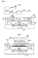
- FIG. 1(A) is a structural view showing the structure of a solder-ball loading apparatus according to an embodiment of the present invention.
- Fig. 1(B) is a view, as seen from the direction of arrow B, illustrating the solder-ball loading apparatus shown in Fig. 1(A) .
- Solder-ball loading apparatus 20 has XY ⁇ suction table 14 that determines and maintains the position for multilayered printed wiring board 10; elevator shaft 12 that vertically moves up and down XY ⁇ suction table 14; ball array mask 16 that has openings corresponding to pads 75 of the multilayered printed wiring board; loading cylinder (cylinder member) 24 that guides solder balls; suction box 26 that provides a negative pressure for loading cylinder 24; ball-removal cylinder 61 that collects excess solder balls; suction box 66 that provides a negative pressure for ball-removal cylinder 61; ball-removal suction device 68 that holds collected solder balls; mask clamp 44 that clamps ball array mask 16; alignment camera 46 that photographs multilayered printed wiring board 10; residue detection sensor 18 that detects the remaining number of solder balls under loading cylinder 24; and solder-ball supply device 22 that supplies solder balls for loading cylinder 24 according to the remaining number of balls detected by residue detection sensor 18.
- Loading cylinder 24 and ball-removal cylinder 61 are arranged in multiple numbers in the Y-direction according to the size of the connection pad region. The number may also be determined according to the size of multiple connection pad regions.
- the Y-direction is arbitrary, and they may be arranged in the X-direction as well.
- XY ⁇ suction table 14 performs positioning, suctioning, holding, adjusting and moving of multilayered printed wiring board 10 onto which solder balls are loaded.
- XY ⁇ suction table 14 may be moved with ball array mask 16 clamped by mask clamp 44 when moving printed wiring board 10.
- Alignment camera 46 detects the alignment mark of multilayered printed wiring board 10 positioned on XY ⁇ suction table 14. According to the detected position, the alignment between multilayered printed wiring board 10 and ball array mask 16 is adjusted.
- Residue detection sensor 18 detects the remaining number of solder balls by an optical method.
- loading cylinder 24 is secured, and ball array mask 16 and printed wiring board 10 are moved.
- a drive unit (XY ⁇ suction table 14) may be set under printed wiring board 10. Accordingly, the risk of a foreign substance being dropped onto the printed wiring board from the drive unit having a movable member may be prevented.
- solder-ball supply unit 22 supplies solder balls as shown in Fig. 2(B) .
- loading cylinder 24 is positioned. Then, by suctioning air from suction section (24B), the air flow between the loading cylinder and the printed wiring board is set in the range of 5 m/sec. to 50 m/sec., and solder balls (78s) are gathered on ball array mask 16 and directly under opening portion (24A) of loading cylinder 24. After that, as shown in Figs.
- solder balls (78s) that have been gathered directly under loading cylinder 24 are moved while ball array mask 16 and printed wiring board 10 are moved, then the balls are dropped onto pads 75 of multilayered printed wiring board 10 through openings (16a) of ball array mask 16. Accordingly, solder balls (78s) are loaded onto all the pads on multilayered printed wiring board 10 one after another.
- loading cylinder 24 is positioned above ball array mask 16, and by suctioning air through opening (24B) of loading cylinder 24, solder balls (78s) are gathered. Then, by horizontally moving ball array mask 16 and printed wiring board 10, gathered solder balls (78s) are moved on ball array mask 16 and dropped onto pads 75 of multilayered printed wiring board 10 through openings (16a) of ball array mask 16. Accordingly, microscopic solder balls (78s) may be securely loaded onto every pad 75 of multilayered printed wiring board 10. Also, since solder balls (78s) are moved without making any contact, unlike cases using a squeegee, the solder balls may be loaded onto pads 75 without damage.
- solder bumps may be uniform. Accordingly, mountability of electronic components such as an IC chip, heat cycle tests after mounting, and tests for environmental resistance such as high-temperature and high-humidity tests show excellent results. Furthermore, since a flat surface is not required, a printed wiring board with an uneven surface may load solder balls appropriately onto its pads. Also, microscopic solder balls may be loaded securely onto pads. Thus, in a printed wiring board having a pad pitch in the range of 60-150 ⁇ m and an opening diameter of the solder resist in the range of 40-100 ⁇ m, all solder bumps may have a uniform bump height.
- solder balls are guided with suction force, solder balls may be prevented from condensing and sticking. Furthermore, by adjusting the number of loading cylinders 24, varieties of works (work-sheet-size multilayered printed wiring boards) may be handled, thus making possible its flexible application on a variety of products and production in small quantities.
- solder-ball loading apparatus of the present invention as shown in Fig. 1(B) , multiple loading cylinders 24 are arranged in the Y-direction in proportion to the width of the work (a work-sheet size multilayered printed wiring board). Therefore, by moving ball array mask 16 and printed wiring board 10 in a direction perpendicular to the direction (the X-direction) in which loading cylinders 24 are lined up, solder balls may be securely loaded onto all pads 75 of multilayered printed wiring board 10.
- solder balls (78s) left on ball array mask 16 may be collected. Accordingly, residual solder balls will not cause trouble such as a breakdown.
- solder bumps manufactured by the method for loading solder balls according to the example and solder bumps manufactured by a conventional method are compared.
- double-sided copper-clad laminate for example, "MCL-E-67” made by Hitachi Chemical Co., Ltd.
- through-hole conductors and conductive circuits are formed on the substrate by a conventional method.
- a conventional method such as " Built-Up Multiple Printed Wiring Board” written by Kiyoshi Takagi, published by the Nikkan Kogyo Shimbun Ltd. on June 20, 2006
- interlayer insulation layers and conductive-circuit layers are alternately laminated and on the outermost conductive-circuit layer, to electrically connect to an IC, pad groups each having a diameter of 150 ⁇ m, a pitch of 150 ⁇ m and an arrangement of 50 ⁇ 50 pads (arranged in grids) are formed.
- connection pads formed from via holes are made as filled vias.
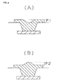
- the degree of surface concavity and convexity relative to the conductor thickness of conductive circuit 158 as shown in Fig. 8(A) , the degree of concavity (the hollowed portion from the top surface) (P1) is preferred to be set (-5) ⁇ m or less, and as shown in Fig. 8(B) , the degree of convexity (the portion protruding from the top flat surface) (P2) is preferred to be set (+5) ⁇ m or less.
- the degree of concavity exceeds 5 ⁇ m (-5 ⁇ m)
- the contact points between solder balls and the connection pads formed from filled vias decrease, causing poor wettability when making solder bumps.
- voids in the solder or missing bumps may often occur.
- the degree of convexity exceeds 5 ⁇ m, the thickness of conductive circuit 158 increases, thus ruling it out for use in products with finer features.
- the printed wiring board manufactured in (1) On the surface (the surface to mount an IC) of the printed wiring board manufactured in (1), a commercially available Rogin-type flux is coated. Then, the printed wiring board is mounted on the suction table of the above-described solder-ball loading apparatus of the present invention, and using a CCD camera, alignment marks on the printed wiring board and ball loading mask are recognized to align the printed wiring board and the ball loading mask.
- the ball loading mask a metal mask with a thickness in the range of 25 ⁇ m-50 ⁇ m made of nickel that has openings with a diameter of 110 ⁇ m corresponding to the pads on the printed wiring board is used.
- Other ball loading masks made of SUS or polyimide may also be used.
- the diameter of the openings formed in the ball loading mask is preferably made 1.1 - 1.5 times as large as the diameter of the balls to be loaded. Then, a loading cylinder of a size in proportion to the pad region (1.2-3 times as big as the pad region) and 200 millimeters in height is positioned over the printed wiring board, while keeping a clearance twice as high as the solder-ball diameter. On the ball loading mask, which is positioned nearby, solder balls containing Sn 63:Pb 37 (made by Hitachi Metals Ltd.) with a diameter of 80 ⁇ m are loaded.
- Sn/Pb solder is used for solder balls.
- a lead-free solder selected from among groups such as Sn with Ag, Cu, In, Bi or Zn may be used.
- solder-ball loading mask and the printed wiring board are removed separately from the solder-ball loading apparatus.
- the printed wiring board manufactured in the above is put into a reflow furnace with a temperature set at 230°C to form solder bumps.
- solder balls are moved by a squeegee and dropped through the ball loading openings to be loaded onto pads.
- solder bumps are picked at random and their bump heights from the top of the solder resist are measured using a laser microscope "VX-8500" made by Keyence Corp.
- connection resistance values is figured as ((connection resistance value after heat cycle tests - initial connection resistance value) / initial connection resistance value) x 100. If the figure exceeds 10%, it is considered to be inferior. number of inferior units Example 0 Comp. Exp. 3 From the above result, it is found that in the present invention, the connection reliability of bumps is high, since the dispersion in bump heights is small.
- loading cylinder 24 is structured with a conductive metal such as SUS stainless steel, nickel, or copper, and grounded to the area where solder-ball loading apparatus 20 is positioned.
- a conductive metal such as SUS stainless steel, nickel, or copper
- the solder balls are securely loaded onto the printed wiring board.
- the following material may also be used: conductive resin containing black lead powder, conductive metal film 23 such as aluminum coated on the surface of the resin member by deposition or the like, or conductive metal foil (23f) laminated on the bottom edge and the interiors of resin member 21.
Landscapes
- Engineering & Computer Science (AREA)
- Manufacturing & Machinery (AREA)
- Microelectronics & Electronic Packaging (AREA)
- Mechanical Engineering (AREA)
- Electric Connection Of Electric Components To Printed Circuits (AREA)
Abstract
[Subject Matter]
To provide a solder-ball loading apparatus for loading microscopic solder balls onto electrodes
[Solution]
By suctioning air through loading cylinder 24 positioned above ball array mask 16, solder balls (78s) are gathered. By horizontally moving printed wiring board 10 and ball array mask 16, solder balls (78s) gathered directly under loading cylinder 24 are moved on ball array mask 16 and dropped onto electrodes 75 of multilayered printed wiring board 10 through openings (16a) of ball array mask 16.
Description
- The present invention relates to a method and apparatus for loading ono a printed wiring board solder balls which will become solder bumps.
- Solder bumps are used for electrical connection between a package substrate and an IC chip. Solder bumps are formed by the following steps:
- (1) a step to print flux on electrodes formed in a package substrate;
- (2) a step to load solder balls onto the electrodes on which the flux is printed; and
- (3) a step to form solder bumps from the solder balls by conducting a reflow.
- In the above step to load solder balls onto electrodes, for example, as described in Patent Publication (1), solder balls are suctioned by a suction head and then loaded onto electrodes; or, as described in Patent Publication (2), using a ball array mask having multiple openings, solder balls are dropped onto electrodes.
- Patent Publication (1): Japanese Patent No.
1975429 - Patent Publication (2): Japanese Laid-Open Patent Application
2001-358450 - Patent Publication (3): Japanese Laid-Open Patent Application
2001-267731 - As ICs become more highly integrated, solder bumps on a package substrate are required to be made with a much smaller diameter and narrower pitches. Consequently, the diameter of solder balls has become even smaller than that of a grain of sand, smaller than 200 µm, and the yield in the above-described method using a suction head has been reduced. Also, in the method using both a ball array mask and a squeegee, the varying height of solder bumps has resulted in lower quality.
- Namely, if the diameter of solder balls becomes smaller, the ratio of the weight to the surface area decreases, thus causing a suction phenomenon among solder balls due to intermolecular forces. Therefore, when the above-described suction head is used, even if air is pumped down from above the electrodes to drop solder balls, the balls stick to the suction head and do not fall. Accordingly, this creates a problem of missing solder bumps.
- On the other hand, when a ball array mask is used, due to the suction phenomenon involving the solder balls, the balls stick together. Therefore, even if a printed wiring board with the loaded ball array mask is tilted, the solder balls do not roll down, thus it is impossible to drop the solder balls through the openings of the ball array mask. When the ball array mask is not tilted, and the solder balls are moved by a squeegee, since the stuck-together solder balls touch the squeegee during the move, the solder balls are damaged. Accordingly, as described above, the height of the solder bumps varies, resulting in low quality. Especially, in a printed wiring board with a substantially uneven surface, such as a built-up multilayered wiring board, it is difficult to move solder balls with a squeegee without damaging the balls.
- The objective of the present invention is to provide a solder-ball loading method and a solder-ball loading apparatus for loading fine solder balls onto pads.
- To achieve the above objective, the present invention according to
Claim 1 relates to a method for loading solder balls: By using a ball array mask having multiple openings corresponding to the pads of a printed wiring board, solder balls that will become solder bumps are loaded onto the pads of the printed wiring board. The method has the following technical features: Above the ball array mask, a cylinder member having an opening portion facing the ball array mask is positioned; by suctioning air using the cylinder member, solder balls are gathered to a section of the ball array mask directly under the cylinder member; and by horizontally moving the ball array mask and the printed wiring board, the solder balls gathered directly under the cylinder member are dropped onto the pads on the printed wiring board through the openings of the ball array mask. - The invention according to Claim 2 relates to a solder-ball loading apparatus which loads onto pads of a printed wiring board solder balls that will become solder bumps. The apparatus has the following technical features: A ball array mask with multiple openings corresponding to the pads of a printed wiring board; a cylinder member positioned above the ball array mask to gather solder balls in a section directly under its opening by suctioning air through the opening; and a conveyor mechanism to horizontally move the ball array mask and the printed wiring board, more specifically, by horizontally moving the ball array mask and the printed wiring board, the solder balls gathered directly under the cylinder member are dropped onto the pads of the printed wiring board through the openings of the ball array mask.
- According to the solder-ball loading method of
Claim 1 and the solder-ball loading apparatus of Claim 2, a cylinder member is positioned above a ball array mask and by suctioning air through the opening portion of the cylinder member, solder balls are gathered, then by horizontally moving the ball array mask and the printed wiring board, the solder balls gathered directly under the cylinder member are moved on the ball array mask and dropped onto the pads of the printed wiring board through the openings in the ball array mask. Accordingly, fine solder balls are securely loaded onto every pad on the printed wiring board. Also, since solder balls are moved without contact, unlike cases using a squeegee, the solder balls may be loaded onto the pads without damage, thus the height of the solder bumps may be uniform. Furthermore, solder balls may be properly loaded onto a printed wiring board having a substantially uneven surface, such as a built-up multilayered wiring board. In addition, since the cylinder member is secured, while the ball array mask and the printed wiring board are moved, in contrast to a case in which the cylinder member is moved, the drive unit may be set under the printed wiring board. Thus, the risk of a foreign substance being dropped onto the printed wiring board from the drive unit having a movable member may be prevented. - According to the solder-ball loading apparatus of Claim 3, multiple cylinder members are arranged in proportion to the width of a printed wiring board. Thus, by simply moving the ball array mask and the printed wiring board in a direction perpendicular to the direction in which the cylinder members are lined up, solder balls are securely loaded onto every pad on the printed wiring board.
- According to the solder-ball loading apparatus of
Claim 4, using the suction cylinder, solder balls remaining on the ball array mask may be collected. Thus, remaining excess solder balls will not become obstacles that may cause trouble. - According to the solder-ball loading apparatus of
Claim 5, when moving solder balls on the ball array mask to feed them, if the solder balls are charged with electricity from colliding with each other, since at least the area of the cylinder member where solder balls come in contact is formed with a conductive material, lightweight solder balls with a small diameter will not stick to the cylinder member due to static electricity. Accordingly, solder balls are securely loaded onto a printed wiring board. - First, the structure of multilayered printed
wiring board 10, which is manufactured by the method and apparatus for loading solder balls according to the First Example of the present invention, is described with reference toFigs. 6-7 .Fig. 6 is a cross-sectional view of multilayered printedwiring board 10, andFig. 7 is a view illustrating multilayered printedwiring board 10 shown inFig. 6 with mountedIC chip 90 and installed ondaughter board 94. As shown inFig. 6 , in multilayered printedwiring board 10,conductive circuits 34 are formed on both surfaces of core substrate 30. The upper surface and the lower surface of core substrate 30 are connected via through-holes 36. - Furthermore, on
conductive circuit 34 on core substrate 30,conductive circuit 58, which forms a conductive circuit layer, is formed via interlayerresin insulation layer 50.Conductive circuit 58 is connected toconductive circuit 34 through via-holes 60. Onconductive circuit 58,conductive circuit 158 is formed via interlayerresin insulation layer 150.Conductive circuit 158 is connected toconductive circuit 58 through viaholes 160 formed in interlayerresin insulation layer 150. - On via
holes 160 andconductive circuit 158, solder-resist layer 70 is formed. Inopenings 71 of solder-resist layer 70, nickel-platedlayer 72 and gold-platedlayer 74 are deposited to formpads 75. Onpads 75 formed on the upper surface, solder bumps (78U) are formed; and onpads 75 formed on the lower surface, BGA (ball grid array) (78D) is formed. - As shown in
Fig. 7 , solder bumps (78U) on the upper surface of multilayered printedwiring board 10 are connected toelectrodes 92 ofIC chip 90. Meanwhile, BGA (78D) on the lower surface is connected tolands 96 ofdaughter board 94. -
Figs. 5 are views illustrating steps to form solder bumps on multilayered printedwiring board 10. As shown inFig. 5(A) , on the surface of multilayered printedwiring board 10, wherepads 75 are formed inopenings 71 of solder-resist layer 70,flux 80 is printed. As shown inFig. 5(B) , ontopads 75 formed on the upper surface of multilayered printedwiring board 10, using the later described solder-ball loading apparatus, microscopic solder balls (78s) (such as made by Hitachi Metals, Ltd. or Tamura Co., with a diameter of 40 µm or larger, but less than 200 µm) are loaded. To deal with products having finer features, solder balls with a diameter less than 200 µm are preferred. If the diameter is less than 40 µm, solder balls become too lightweight, and it is difficult to drop them onto pads. On the other hand, if the diameter is 200 µm or larger, solder balls become too heavy to be gathered into the cylinder member, thus the number of pads without solder balls may increase. - Then, as shown in
Fig. 5(C) , ontopads 75 on the lower surface of multilayered printedwiring board 10, using a suction head related to conventional technology disclosed in Patent Publication (1), solder balls (78L) with a regular diameter (250 µm in diameter) are suctioned and loaded. Then, after being heated in a reflow furnace, as shown inFig. 6 , on the upper surface of multilayered printedwiring board 10, solder bumps (78U), for example 2,000 of them, are formed at a pitch in the range of 60-150 µm; and on the lower surface, BGA (78D), for example, 250 of them, are formed at a 2-mm pitch. If the pitch is smaller than 60 µm, it is difficult to manufacture solder balls appropriate to such a pitch. If the pitch exceeds 150 µm, the solder balls may be easily produced by the method of the present invention, but may also be produced by conventional methods as well. Furthermore, as shown inFig. 7 , by reflow,IC chip 90 is mounted through solder bumps (78U), and then multilayered printedwiring board 10 with mountedIC chip 90 is installed ondaughter board 94 via BGA (78D). - A solder-ball loading apparatus, by which fine solder balls (78s) (with a diameter less than 200 µm) are loaded onto pads of a multilayered printed wiring board as described above in reference to
Fig. 5(B) , is described in reference toFigs. 1. Fig. 1(A) is a structural view showing the structure of a solder-ball loading apparatus according to an embodiment of the present invention.Fig. 1(B) is a view, as seen from the direction of arrow B, illustrating the solder-ball loading apparatus shown inFig. 1(A) . - Solder-
ball loading apparatus 20 has XYθ suction table 14 that determines and maintains the position for multilayered printedwiring board 10;elevator shaft 12 that vertically moves up and down XYθ suction table 14;ball array mask 16 that has openings corresponding topads 75 of the multilayered printed wiring board; loading cylinder (cylinder member) 24 that guides solder balls;suction box 26 that provides a negative pressure for loadingcylinder 24; ball-removal cylinder 61 that collects excess solder balls;suction box 66 that provides a negative pressure for ball-removal cylinder 61; ball-removal suction device 68 that holds collected solder balls;mask clamp 44 that clampsball array mask 16;alignment camera 46 that photographs multilayered printedwiring board 10;residue detection sensor 18 that detects the remaining number of solder balls underloading cylinder 24; and solder-ball supply device 22 that supplies solder balls for loadingcylinder 24 according to the remaining number of balls detected byresidue detection sensor 18. -
Loading cylinder 24 and ball-removal cylinder 61 are arranged in multiple numbers in the Y-direction according to the size of the connection pad region. The number may also be determined according to the size of multiple connection pad regions. Here, the Y-direction is arbitrary, and they may be arranged in the X-direction as well. XYθ suction table 14 performs positioning, suctioning, holding, adjusting and moving of multilayered printedwiring board 10 onto which solder balls are loaded. Here, XYθ suction table 14 may be moved withball array mask 16 clamped bymask clamp 44 when moving printedwiring board 10.Alignment camera 46 detects the alignment mark of multilayered printedwiring board 10 positioned on XYθ suction table 14. According to the detected position, the alignment between multilayered printedwiring board 10 andball array mask 16 is adjusted.Residue detection sensor 18 detects the remaining number of solder balls by an optical method. - In solder-
ball loading apparatus 20 according to the First Embodiment,loading cylinder 24 is secured, andball array mask 16 and printedwiring board 10 are moved. Thus, in contrast to cases in whichloading cylinder 24 is moved, a drive unit (XYθ suction table 14) may be set under printedwiring board 10. Accordingly, the risk of a foreign substance being dropped onto the printed wiring board from the drive unit having a movable member may be prevented. - In the following, using solder-
ball loading apparatus 20, steps to load solder balls are described in reference toFigs. 2-4 .
(1) Recognizing and adjusting the position of the multilayered printed wiring board
As shown inFig. 2(A) , alignment mark (34M) of multilayered printedwiring board 10 is recognized byalignment camera 46, and the position of multilayered printedwiring board 10 relative toball array mask 16 is adjusted using XYθ suction table 14. Namely, the position is adjusted so that openings (16a) ofball array mask 16 correspond topads 75 of multilayered printedwiring board 10 respectively. Here, for illustration purposes, only a sheet of multilayered printedwiring board 10 is shown. However, actually, solder balls are loaded onto a work-sheet-size multilayered printed wiring board containing multiple sheets of multilayered printed wiring boards.
Then, after solder bumps are formed, each multilayered printed wiring board is cut out - (2) Supplying solder balls
As shown inFig. 2(B) , a predetermined number of solder balls (78s) are supplied from solder-ball supply unit 22 toloading cylinder 24. - (3) Loading solder balls
As shown inFig. 3(A) , overball array mask 16, while keeping a predetermined clearance (for example, 100%-300% of the ball diameter),loading cylinder 24 is positioned. Then, by suctioning air from suction section (24B), the air flow between the loading cylinder and the printed wiring board is set in the range of 5 m/sec. to 50 m/sec., and solder balls (78s) are gathered onball array mask 16 and directly under opening portion (24A) ofloading cylinder 24. After that, as shown inFigs. 3(B) ,4(A) ,1(B) and 1(A) , printedwiring board 10 andball array mask 16 are horizontally moved along the X-axis using XYθ suction table 14. By doing so, solder balls (78s) that have been gathered directly underloading cylinder 24 are moved whileball array mask 16 and printedwiring board 10 are moved, then the balls are dropped ontopads 75 of multilayered printedwiring board 10 through openings (16a) ofball array mask 16. Accordingly, solder balls (78s) are loaded onto all the pads on multilayered printedwiring board 10 one after another. - (4) Removing the stuck solder balls
As shown inFig. 4(B) , by moving printedwiring board 10 andball array mask 16, excess solder balls (78s) are guided to the area where there are no openings (16a) ofball array mask 16, then suctioned and removed through ball-removal cylinder 61. - (5) Removing the substrate
From XYθ suction table 14, multilayered printedwiring board 10 is removed. - According to the method for loading solder balls of the present invention and solder-
ball loading apparatus 20,loading cylinder 24 is positioned aboveball array mask 16, and by suctioning air through opening (24B) ofloading cylinder 24, solder balls (78s) are gathered. Then, by horizontally movingball array mask 16 and printedwiring board 10, gathered solder balls (78s) are moved onball array mask 16 and dropped ontopads 75 of multilayered printedwiring board 10 through openings (16a) ofball array mask 16. Accordingly, microscopic solder balls (78s) may be securely loaded onto everypad 75 of multilayered printedwiring board 10. Also, since solder balls (78s) are moved without making any contact, unlike cases using a squeegee, the solder balls may be loaded ontopads 75 without damage. Thus, the height of solder bumps (78U) may be uniform. Accordingly, mountability of electronic components such as an IC chip, heat cycle tests after mounting, and tests for environmental resistance such as high-temperature and high-humidity tests show excellent results.
Furthermore, since a flat surface is not required, a printed wiring board with an uneven surface may load solder balls appropriately onto its pads. Also, microscopic solder balls may be loaded securely onto pads. Thus, in a printed wiring board having a pad pitch in the range of 60-150 µm and an opening diameter of the solder resist in the range of 40-100 µm, all solder bumps may have a uniform bump height. - In addition, since solder balls are guided with suction force, solder balls may be prevented from condensing and sticking. Furthermore, by adjusting the number of
loading cylinders 24, varieties of works (work-sheet-size multilayered printed wiring boards) may be handled, thus making possible its flexible application on a variety of products and production in small quantities. - According to the solder-ball loading apparatus of the present invention, as shown in
Fig. 1(B) ,multiple loading cylinders 24 are arranged in the Y-direction in proportion to the width of the work (a work-sheet size multilayered printed wiring board). Therefore, by movingball array mask 16 and printedwiring board 10 in a direction perpendicular to the direction (the X-direction) in whichloading cylinders 24 are lined up, solder balls may be securely loaded onto allpads 75 of multilayered printedwiring board 10. - Moreover, by using ball-
removal cylinder 61, remaining solder balls (78s) left onball array mask 16 may be collected. Accordingly, residual solder balls will not cause trouble such as a breakdown. - In the following, a comparison test and its results are described. In the test, solder bumps manufactured by the method for loading solder balls according to the example and solder bumps manufactured by a conventional method are compared.
- As a starting material, double-sided copper-clad laminate (for example, "MCL-E-67" made by Hitachi Chemical Co., Ltd.) is used and through-hole conductors and conductive circuits are formed on the substrate by a conventional method. Then, using a conventional method (such as "Built-Up Multiple Printed Wiring Board" written by Kiyoshi Takagi, published by the Nikkan Kogyo Shimbun Ltd. on June 20, 2006), interlayer insulation layers and conductive-circuit layers are alternately laminated and on the outermost conductive-circuit layer, to electrically connect to an IC, pad groups each having a diameter of 150 µm, a pitch of 150 µm and an arrangement of 50 × 50 pads (arranged in grids) are formed. On top of them, a commercially available solder resist is formed, and openings with a diameter of 100 µm are formed on the pads by a photographic method. Here, connection pads formed from via holes (solder bumps formed directly on the via holes) are made as filled vias. Regarding the degree of surface concavity and convexity relative to the conductor thickness of
conductive circuit 158, as shown inFig. 8(A) , the degree of concavity (the hollowed portion from the top surface) (P1) is preferred to be set (-5) µm or less, and as shown inFig. 8(B) , the degree of convexity (the portion protruding from the top flat surface) (P2) is preferred to be set (+5) µm or less. If the degree of concavity exceeds 5 µm (-5 µm), the contact points between solder balls and the connection pads formed from filled vias decrease, causing poor wettability when making solder bumps. As a result, voids in the solder or missing bumps may often occur. On the other hand, if the degree of convexity exceeds 5 µm, the thickness ofconductive circuit 158 increases, thus ruling it out for use in products with finer features. - On the surface (the surface to mount an IC) of the printed wiring board manufactured in (1), a commercially available Rogin-type flux is coated. Then, the printed wiring board is mounted on the suction table of the above-described solder-ball loading apparatus of the present invention, and using a CCD camera, alignment marks on the printed wiring board and ball loading mask are recognized to align the printed wiring board and the ball loading mask. Here, as for the ball loading mask, a metal mask with a thickness in the range of 25 µm-50 µm made of nickel that has openings with a diameter of 110 µm corresponding to the pads on the printed wiring board is used. Other ball loading masks made of SUS or polyimide may also be used. The diameter of the openings formed in the ball loading mask is preferably made 1.1 - 1.5 times as large as the diameter of the balls to be loaded. Then, a loading cylinder of a size in proportion to the pad region (1.2-3 times as big as the pad region) and 200 millimeters in height is positioned over the printed wiring board, while keeping a clearance twice as high as the solder-ball diameter. On the ball loading mask, which is positioned nearby, solder balls containing Sn 63:Pb 37 (made by Hitachi Metals Ltd.) with a diameter of 80 µm are loaded.
- In this example, Sn/Pb solder is used for solder balls. However, a lead-free solder selected from among groups such as Sn with Ag, Cu, In, Bi or Zn may be used. By suctioning air through the upper portion of the loading cylinder (24B), air flow speed between the loading cylinder and the printed wiring board is adjusted in the range of 5-35 m/sec. to gather the balls in the loading cylinder. Then, by moving
ball array mask 16 and printedwiring board 10 at a speed of 40 mm/sec., solder balls are moved, dropped onto the pads through the openings of the ball loading mask, and loaded on the pads. Next, after removing excess solder balls from the ball loading mask, the solder-ball loading mask and the printed wiring board are removed separately from the solder-ball loading apparatus. Lastly, the printed wiring board manufactured in the above is put into a reflow furnace with a temperature set at 230°C to form solder bumps. - Except that the method for supplying pads with solder balls is changed, the rest is the same as in the Example. Namely, using a conventional method, solder balls are moved by a squeegee and dropped through the ball loading openings to be loaded onto pads.
- After the reflow process, 50 solder bumps are picked at random and their bump heights from the top of the solder resist are measured using a laser microscope "VX-8500" made by Keyence Corp.
-
average height of bumps dispersion of bump heights Example 35.22 µm 1.26 Comp. Exp. 32.64 µm 2.00 - In addition, 100 units of printed wiring boards obtained in the Example and the Comparative Example were prepared, ICs were mounted and the electrical continuity was checked to calculate the yield. The resulting yield was 100% among the units of the Example, but among the units of the Comparative Example, the yield was 76%. Then, ten units of each example that showed satisfactory results were picked at random and put under heat cycle tests. A heat cycle test, -55×5 minutes ⇔ 125×5 minutes, was conducted 1,000 times. After that, the change in connection resistance values on a certain circuit, which is connected from the bottom surface (the opposite surface to the IC mounted surface) of a printed wiring board via an IC to the bottom surface again, was measured. The change in connection resistance values is figured as ((connection resistance value after heat cycle tests - initial connection resistance value) / initial connection resistance value) x 100. If the figure exceeds 10%, it is considered to be inferior.
number of inferior units Example 0 Comp. Exp. 3 - In the Example,
loading cylinder 24 is structured with a conductive metal such as SUS stainless steel, nickel, or copper, and grounded to the area where solder-ball loading apparatus 20 is positioned. Here, when moving solder balls onball array mask 16 to feed them, even if the solder balls are charged from colliding with each other, lightweight and small-diameter solder balls will not stick toloading cylinder 24 due to static electricity. Accordingly, the solder balls are securely loaded onto the printed wiring board. In addition, as for loadingcylinder 24, the following material may also be used: conductive resin containing black lead powder, conductive metal film 23 such as aluminum coated on the surface of the resin member by deposition or the like, or conductive metal foil (23f) laminated on the bottom edge and the interiors of resin member 21. -
- [
Figs. 1] Fig. 1(A) is a structural view illustrating the solder-ball loading apparatus according to an embodiment of the present invention; and -
Fig. 1(B) is a view illustrating the solder-ball loading apparatus shown inFig. 1(A) , as seen from the direction of arrow B. - [
Figs. 2] Fig. 2(A) is a view illustrating how to position a multilayered printed wiring board; andFig. 2(B) is a view illustrating how to supply solder balls for a loading cylinder. - [
Figs. 3] Fig. 3(A) is a view illustrating how to gather solder balls using a loading cylinder; andFig. 3(B) is a view illustrating how to gather and guide solder balls using the loading cylinder. - [
Figs. 4] Fig. 4(A) is a view illustrating how to drop solder balls onto pads; andFig. 4(B) is a view illustrating how to remove solder balls using a ball-removal cylinder. - [
Figs. 5] Figs. 5(A), 5(B) and 5(C) are views illustrating manufacturing steps of a multilayered printed wiring board. - [
Fig. 6] Fig. 6 is a cross-sectional view of a multilayered printed wiring board. - [
Fig. 7] Fig. 7 is a cross-sectional view illustrating a multilayered printed wiring board with a mounted IC chip and installed on a daughter board. - [
Figs. 8] Figs. 8 are views illustrating filled vias in the First Example. -
- 10
- printed wiring board
- 12
- elevator shaft
- 14
- XYθ suction table
- 16
- ball array mask
- 16a
- opening
- 18
- residue detection sensor
- 20
- solder-ball loading apparatus
- 22
- solder-ball supply device
- 24
- loading cylinder (loading member)
- 26
- suction box
- 44
- mask clamp
- 46
- alignment camera
- 61
- ball-removal cylinder
- 66
- suction box
- 68
- stuck-ball removal suction device
- 75
- pad
- 80
- flux
Claims (5)
- A method of loading solder balls, wherein
using a ball array mask having multiple openings that correspond to pads on a printed wiring board, solder balls which will become as solder bumps are loaded onto the pads on the printed wiring board,
above the ball array mask, a cylinder member having an opening portion facing the ball array mask is positioned,
by suctioning air using the cylinder member, solder balls are gathered on the ball array mask directly under the cylinder member, and
by horizontally moving the ball array mask and the printed wiring board, solder balls gathered directly under the cylinder member are dropped onto the pads of the printed wiring board through the openings of the ball array mask. - A solder-ball loading apparatus, wherein solder balls which will become solder bumps are loaded onto pads of a printed wiring board, comprising:a ball array mask having multiple openings that correspond to pads of the printed wiring board;a cylinder member positioned above the ball array mask that gathers solder balls directly under its opening by suctioning air through the opening portion; anda conveyor mechanism for horizontally moving the ball array mask and the printed wiring board, wherein by horizontally moving the ball array mask and the printed wiring board, solder balls gathered directly under the cylinder member are dropped onto the pads of the printed wiring board through the openings of the ball array mask.
- The solder-ball loading apparatus according to Claim 2, wherein multiple cylinder members are arranged in proportion to the width of the printed wiring board.
- The solder-ball loading apparatus according to Claim 2 or Claim 3, further comprising a suction cylinder to collect solder balls remaining on the ball array mask.
- The solder-ball loading apparatus according to any one of Claims 2-4, wherein at least in the section that comes in contact with the solder balls, the cylinder member is structured with a conductive material.
Applications Claiming Priority (2)
| Application Number | Priority Date | Filing Date | Title |
|---|---|---|---|
| JP2006019064 | 2006-01-27 | ||
| PCT/JP2007/051273 WO2007086508A1 (en) | 2006-01-27 | 2007-01-26 | Method and apparatus for mounting solder ball |
Publications (1)
| Publication Number | Publication Date |
|---|---|
| EP1978794A1 true EP1978794A1 (en) | 2008-10-08 |
Family
ID=38309294
Family Applications (1)
| Application Number | Title | Priority Date | Filing Date |
|---|---|---|---|
| EP07707505A Withdrawn EP1978794A1 (en) | 2006-01-27 | 2007-01-26 | Method and apparatus for mounting solder ball |
Country Status (7)
| Country | Link |
|---|---|
| US (2) | US8091766B2 (en) |
| EP (1) | EP1978794A1 (en) |
| JP (1) | JP4592762B2 (en) |
| KR (1) | KR20080014143A (en) |
| CN (1) | CN101356866B (en) |
| TW (1) | TWI413471B (en) |
| WO (1) | WO2007086508A1 (en) |
Families Citing this family (7)
| Publication number | Priority date | Publication date | Assignee | Title |
|---|---|---|---|---|
| JP5021473B2 (en) * | 2005-06-30 | 2012-09-05 | イビデン株式会社 | Method for manufacturing printed wiring board |
| JP5389748B2 (en) * | 2010-06-18 | 2014-01-15 | 日本メクトロン株式会社 | Electronic component surface mounting method and printed circuit board manufactured using the method |
| KR20140019173A (en) | 2012-08-06 | 2014-02-14 | 삼성전기주식회사 | Packaging method using solder coating-ball and package thereby |
| CN104639393A (en) * | 2015-01-07 | 2015-05-20 | 烽火通信科技股份有限公司 | Passive optical network flow whole-network acquisition device and passive optical network flow whole-network acquisition method |
| US10879102B2 (en) * | 2017-08-07 | 2020-12-29 | Boston Process Technologies, Inc | Flux-free solder ball mount arrangement |
| CN110534451A (en) * | 2018-05-25 | 2019-12-03 | 唐虞企业股份有限公司 | A conductive terminal placing device and a conducting terminal placing method thereof |
| DE102020111820A1 (en) | 2020-04-30 | 2021-11-04 | Friedrich-Alexander-Universität Erlangen - Nürnberg | Electrode structure for guiding a charged particle beam |
Family Cites Families (10)
| Publication number | Priority date | Publication date | Assignee | Title |
|---|---|---|---|---|
| JPH06105731B2 (en) | 1990-03-14 | 1994-12-21 | 新日本製鐵株式▲会▼社 | Bump transfer method and apparatus |
| US6162661A (en) * | 1997-05-30 | 2000-12-19 | Tessera, Inc. | Spacer plate solder ball placement fixture and methods therefor |
| US5921458A (en) * | 1997-06-25 | 1999-07-13 | Fan; Kuang-Shu | Integrated circuit solder ball implant machine |
| JP2001267731A (en) * | 2000-01-13 | 2001-09-28 | Hitachi Ltd | Method of manufacturing electronic component with bump and method of manufacturing electronic component |
| JP3962197B2 (en) * | 2000-03-01 | 2007-08-22 | 株式会社日立製作所 | Bump forming system |
| JP3436355B2 (en) | 2000-06-12 | 2003-08-11 | 株式会社モリカワ | Solder ball mounting device |
| JP4130526B2 (en) * | 2000-11-10 | 2008-08-06 | 株式会社日立製作所 | Bump forming method and apparatus therefor |
| JP3635068B2 (en) * | 2002-03-06 | 2005-03-30 | 株式会社日立製作所 | Bump forming device |
| KR100798662B1 (en) * | 2004-08-04 | 2008-01-28 | 이비덴 가부시키가이샤 | Solder Ball Mounting Method and Solder Ball Mounting Device |
| US7472473B2 (en) | 2006-04-26 | 2009-01-06 | Ibiden Co., Ltd. | Solder ball loading apparatus |
-
2007
- 2007-01-24 TW TW096102637A patent/TWI413471B/en active
- 2007-01-26 CN CN2007800011184A patent/CN101356866B/en not_active Expired - Fee Related
- 2007-01-26 JP JP2007556015A patent/JP4592762B2/en active Active
- 2007-01-26 KR KR1020087000091A patent/KR20080014143A/en not_active Ceased
- 2007-01-26 WO PCT/JP2007/051273 patent/WO2007086508A1/en not_active Ceased
- 2007-01-26 EP EP07707505A patent/EP1978794A1/en not_active Withdrawn
-
2008
- 2008-07-28 US US12/180,830 patent/US8091766B2/en active Active
-
2011
- 2011-10-12 US US13/271,531 patent/US20120067938A1/en not_active Abandoned
Also Published As
| Publication number | Publication date |
|---|---|
| WO2007086508A1 (en) | 2007-08-02 |
| KR20080014143A (en) | 2008-02-13 |
| TW200746965A (en) | 2007-12-16 |
| US8091766B2 (en) | 2012-01-10 |
| CN101356866A (en) | 2009-01-28 |
| JPWO2007086508A1 (en) | 2009-06-25 |
| US20120067938A1 (en) | 2012-03-22 |
| TWI413471B (en) | 2013-10-21 |
| JP4592762B2 (en) | 2010-12-08 |
| CN101356866B (en) | 2010-10-06 |
| US20090026250A1 (en) | 2009-01-29 |
Similar Documents
| Publication | Publication Date | Title |
|---|---|---|
| US8001683B2 (en) | Solder ball loading method | |
| JP5021472B2 (en) | Method for manufacturing printed wiring board | |
| US7866529B2 (en) | Solder ball loading method and solder ball loading unit | |
| US20120067938A1 (en) | Method and apparatus for loading solder balls | |
| JP5056491B2 (en) | Solder ball mounting device | |
| JP4118283B2 (en) | Solder ball mounting method and solder ball mounting apparatus | |
| JP4118286B2 (en) | Solder ball mounting method | |
| JP4118284B2 (en) | Solder ball mounting apparatus and solder ball mounting method | |
| JP4118285B2 (en) | Solder ball mounting apparatus and solder ball mounting method | |
| JP2014049567A (en) | Solder ball mounting device |
Legal Events
| Date | Code | Title | Description |
|---|---|---|---|
| PUAI | Public reference made under article 153(3) epc to a published international application that has entered the european phase |
Free format text: ORIGINAL CODE: 0009012 |
|
| 17P | Request for examination filed |
Effective date: 20080213 |
|
| AK | Designated contracting states |
Kind code of ref document: A1 Designated state(s): DE GB |
|
| DAX | Request for extension of the european patent (deleted) | ||
| RBV | Designated contracting states (corrected) |
Designated state(s): DE GB |
|
| STAA | Information on the status of an ep patent application or granted ep patent |
Free format text: STATUS: THE APPLICATION IS DEEMED TO BE WITHDRAWN |
|
| 18D | Application deemed to be withdrawn |
Effective date: 20090801 |