EP1976118A1 - Surface acoustic wave device and boundary acoustic wave device - Google Patents
Surface acoustic wave device and boundary acoustic wave device Download PDFInfo
- Publication number
- EP1976118A1 EP1976118A1 EP06823270A EP06823270A EP1976118A1 EP 1976118 A1 EP1976118 A1 EP 1976118A1 EP 06823270 A EP06823270 A EP 06823270A EP 06823270 A EP06823270 A EP 06823270A EP 1976118 A1 EP1976118 A1 EP 1976118A1
- Authority
- EP
- European Patent Office
- Prior art keywords
- acoustic wave
- wave filter
- piezoelectric substrate
- surface acoustic
- support layer
- Prior art date
- Legal status (The legal status is an assumption and is not a legal conclusion. Google has not performed a legal analysis and makes no representation as to the accuracy of the status listed.)
- Withdrawn
Links
Images




Classifications
-
- H—ELECTRICITY
- H03—ELECTRONIC CIRCUITRY
- H03H—IMPEDANCE NETWORKS, e.g. RESONANT CIRCUITS; RESONATORS
- H03H9/00—Networks comprising electromechanical or electro-acoustic elements; Electromechanical resonators
- H03H9/70—Multiple-port networks for connecting several sources or loads, working on different frequencies or frequency bands, to a common load or source
- H03H9/72—Networks using surface acoustic waves
- H03H9/725—Duplexers
-
- H—ELECTRICITY
- H03—ELECTRONIC CIRCUITRY
- H03H—IMPEDANCE NETWORKS, e.g. RESONANT CIRCUITS; RESONATORS
- H03H9/00—Networks comprising electromechanical or electro-acoustic elements; Electromechanical resonators
- H03H9/02—Details
- H03H9/05—Holders or supports
- H03H9/0538—Constructional combinations of supports or holders with electromechanical or other electronic elements
- H03H9/0566—Constructional combinations of supports or holders with electromechanical or other electronic elements for duplexers
- H03H9/0576—Constructional combinations of supports or holders with electromechanical or other electronic elements for duplexers including surface acoustic wave [SAW] devices
-
- H—ELECTRICITY
- H03—ELECTRONIC CIRCUITRY
- H03H—IMPEDANCE NETWORKS, e.g. RESONANT CIRCUITS; RESONATORS
- H03H9/00—Networks comprising electromechanical or electro-acoustic elements; Electromechanical resonators
- H03H9/02—Details
- H03H9/05—Holders or supports
- H03H9/10—Mounting in enclosures
- H03H9/1064—Mounting in enclosures for surface acoustic wave [SAW] devices
- H03H9/1092—Mounting in enclosures for surface acoustic wave [SAW] devices the enclosure being defined by a cover cap mounted on an element forming part of the surface acoustic wave [SAW] device on the side of the IDT's
-
- H—ELECTRICITY
- H10—SEMICONDUCTOR DEVICES; ELECTRIC SOLID-STATE DEVICES NOT OTHERWISE PROVIDED FOR
- H10W—GENERIC PACKAGES, INTERCONNECTIONS, CONNECTORS OR OTHER CONSTRUCTIONAL DETAILS OF DEVICES COVERED BY CLASS H10
- H10W72/00—Interconnections or connectors in packages
- H10W72/01—Manufacture or treatment
- H10W72/012—Manufacture or treatment of bump connectors, dummy bumps or thermal bumps
-
- H—ELECTRICITY
- H10—SEMICONDUCTOR DEVICES; ELECTRIC SOLID-STATE DEVICES NOT OTHERWISE PROVIDED FOR
- H10W—GENERIC PACKAGES, INTERCONNECTIONS, CONNECTORS OR OTHER CONSTRUCTIONAL DETAILS OF DEVICES COVERED BY CLASS H10
- H10W72/00—Interconnections or connectors in packages
- H10W72/90—Bond pads, in general
- H10W72/921—Structures or relative sizes of bond pads
- H10W72/922—Bond pads being integral with underlying chip-level interconnections
- H10W72/9223—Bond pads being integral with underlying chip-level interconnections with redistribution layers [RDL]
-
- H—ELECTRICITY
- H10—SEMICONDUCTOR DEVICES; ELECTRIC SOLID-STATE DEVICES NOT OTHERWISE PROVIDED FOR
- H10W—GENERIC PACKAGES, INTERCONNECTIONS, CONNECTORS OR OTHER CONSTRUCTIONAL DETAILS OF DEVICES COVERED BY CLASS H10
- H10W72/00—Interconnections or connectors in packages
- H10W72/90—Bond pads, in general
- H10W72/921—Structures or relative sizes of bond pads
- H10W72/923—Bond pads having multiple stacked layers
-
- H—ELECTRICITY
- H10—SEMICONDUCTOR DEVICES; ELECTRIC SOLID-STATE DEVICES NOT OTHERWISE PROVIDED FOR
- H10W—GENERIC PACKAGES, INTERCONNECTIONS, CONNECTORS OR OTHER CONSTRUCTIONAL DETAILS OF DEVICES COVERED BY CLASS H10
- H10W72/00—Interconnections or connectors in packages
- H10W72/90—Bond pads, in general
- H10W72/921—Structures or relative sizes of bond pads
- H10W72/923—Bond pads having multiple stacked layers
- H10W72/9232—Bond pads having multiple stacked layers with additional elements interposed between layers
-
- H—ELECTRICITY
- H10—SEMICONDUCTOR DEVICES; ELECTRIC SOLID-STATE DEVICES NOT OTHERWISE PROVIDED FOR
- H10W—GENERIC PACKAGES, INTERCONNECTIONS, CONNECTORS OR OTHER CONSTRUCTIONAL DETAILS OF DEVICES COVERED BY CLASS H10
- H10W72/00—Interconnections or connectors in packages
- H10W72/90—Bond pads, in general
- H10W72/941—Dispositions of bond pads
- H10W72/9415—Dispositions of bond pads relative to the surface, e.g. recessed, protruding
-
- H—ELECTRICITY
- H10—SEMICONDUCTOR DEVICES; ELECTRIC SOLID-STATE DEVICES NOT OTHERWISE PROVIDED FOR
- H10W—GENERIC PACKAGES, INTERCONNECTIONS, CONNECTORS OR OTHER CONSTRUCTIONAL DETAILS OF DEVICES COVERED BY CLASS H10
- H10W72/00—Interconnections or connectors in packages
- H10W72/90—Bond pads, in general
- H10W72/941—Dispositions of bond pads
- H10W72/942—Dispositions of bond pads relative to underlying supporting features, e.g. bond pads, RDLs or vias
-
- H—ELECTRICITY
- H10—SEMICONDUCTOR DEVICES; ELECTRIC SOLID-STATE DEVICES NOT OTHERWISE PROVIDED FOR
- H10W—GENERIC PACKAGES, INTERCONNECTIONS, CONNECTORS OR OTHER CONSTRUCTIONAL DETAILS OF DEVICES COVERED BY CLASS H10
- H10W72/00—Interconnections or connectors in packages
- H10W72/90—Bond pads, in general
- H10W72/941—Dispositions of bond pads
- H10W72/944—Dispositions of multiple bond pads
- H10W72/9445—Top-view layouts, e.g. mirror arrays
-
- H—ELECTRICITY
- H10—SEMICONDUCTOR DEVICES; ELECTRIC SOLID-STATE DEVICES NOT OTHERWISE PROVIDED FOR
- H10W—GENERIC PACKAGES, INTERCONNECTIONS, CONNECTORS OR OTHER CONSTRUCTIONAL DETAILS OF DEVICES COVERED BY CLASS H10
- H10W72/00—Interconnections or connectors in packages
- H10W72/90—Bond pads, in general
- H10W72/951—Materials of bond pads
- H10W72/952—Materials of bond pads comprising metals or metalloids, e.g. PbSn, Ag or Cu
Definitions
- the present invention relates to a surface acoustic wave device and a boundary acoustic wave device.
- WLCSP wafer-level chip-size packaging
- a surface acoustic wave device includes a piezoelectric substrate 1 and a resin substrate 7 that faces the piezoelectric substrate 1.
- the piezoelectric substrate 1 includes a conductor pattern having an IDT (a comb-shaped electrode) 2, a reflector 3, and a pad 4 formed thereon.
- the resin substrate 7 includes an external electrode 8.
- the piezoelectric substrate 1. and the resin substrate 7 are bonded and sealed by light curable resins 6a and 6b.
- the pad 4 is electrically connected to the external electrode 8 (refer to, for example, Patent Document 1).
- the present invention provides a surface acoustic wave device and a boundary acoustic wave device that can reduce capacitive coupling between signal lines.
- the present invention provides a surface acoustic wave device having the following structure.
- a surface acoustic wave device includes a piezoelectric substrate, a cover joined to the piezoelectric substrate with a support layer therebetween and with a spacing kept therebetween, and a transmission surface acoustic wave filter and a reception surface acoustic wave filter formed on a major surface of the piezoelectric substrate adjacent to the cover and inside the support layer. External electrodes are provided on the side of the cover opposite that facing the piezoelectric substrate.
- the external electrodes include an antenna terminal electrically connected to the transmission surface acoustic wave filter and the reception surface acoustic wave filter, a transmission input terminal electrically connected to the transmission surface acoustic wave filter, and a reception output terminal electrically connected to the reception surface acoustic wave filter
- the reception surface acoustic wave filter is electrically connected to the antenna terminal using an interconnection line
- the interconnection line includes (a) a piezoelectric substrate line formed on the piezoelectric substrate, (b) a cover line disposed on one of an upper surface and a lower surface of the cover, and (c) a via line that passes through the support layer and the cover so as to connect one end of the piezoelectric substrate line to one end of the cover line,
- Such a structure can reduce capacitive coupling between signal lines by reducing the length of the piezoelectric line or separating the piezoelectric line disposed on the piezoelectric substrate of the interconnection line used for electrically connecting the reception surface acoustic wave filter to the antenna terminal using the cover line and the via line.
- the reception surface acoustic wave filter is a balanced surface acoustic wave filter including one unbalanced signal terminal to which an unbalanced signal is input and two balanced signal terminals that output balanced signals, and the antenna terminal is electrically connected to the unbalanced signal terminal.
- the reception output terminal is electrically connected to the balanced signal terminals.
- Such a structure can provide a balanced surface acoustic wave filter having, in particular, an excellent balanced characteristic.
- reception output terminal may be a pair of external electrodes, each connected to a corresponding one of the two balanced signal terminals of the balanced filter.
- the present invention further provides a surface acoustic wave device having the following structure.
- a surface acoustic wave device includes a piezoelectric substrate, a cover joined to the piezoelectric substrate with a support layer therebetween and with a spacing kept therebetween, and a transmission surface acoustic wave filter and a reception surface acoustic wave filter formed on a major surface of the piezoelectric substrate adjacent to the cover and inside the support layer.
- External electrodes are provided on the side of the cover opposite that facing the piezoelectric substrate.
- the external electrodes include an antenna terminal electrically connected to the transmission surface acoustic wave filter and the reception surface acoustic wave filter, a transmission input terminal electrically connected to the transmission surface acoustic wave filter, and a reception output terminal electrically connected to the reception surface acoustic wave filter.
- the transmission surface acoustic wave filter includes a plurality of series-connected surface acoustic wave resonators.
- An interconnection line that electrically connects at least one pair of the neighboring series-connected surface acoustic wave resonators includes (a) at least one cover line disposed on one of an upper surface and a lower surface of the cover and (b) at least one pair of via lines that passes through at least the support layer so as to connect the at least one cover line to one of the at least one pair of the neighboring series-connected surface acoustic wave resonators and the other surface acoustic wave resonator.
- Such a structure can reduce capacitive coupling between signal lines by removing a line disposed on the piezoelectric substrate of the interconnection line used for electrically connecting the at least one pair of neighboring series-connected surface acoustic wave resonators of the transmission surface acoustic wave filter using the cover line and the via line, by reducing the length of the line disposed on the piezoelectric substrate, or by separating the line disposed on the piezoelectric substrate.
- the present invention further provides a surface acoustic wave device having the following structure.
- a surface acoustic wave device includes a piezoelectric substrate, a cover joined to the piezoelectric substrate with a support layer therebetween and with a spacing kept therebetween, and a transmission surface acoustic wave filter and a reception surface acoustic wave filter formed on a major surface of the piezoelectric substrate adjacent to the cover and inside the support layer.
- External electrodes are provided on the side of the cover opposite that facing the piezoelectric substrate.
- the external electrodes include an antenna terminal electrically connected to the transmission surface acoustic wave filter and the reception surface acoustic wave filter, a transmission input terminal electrically connected to the transmission surface acoustic wave filter, and a reception output terminal electrically connected to the reception surface acoustic wave filter.
- the reception surface acoustic wave filter includes a plurality of series-connected surface acoustic wave resonators.
- An interconnection line that electrically connects at least one pair of the neighboring series-connected surface acoustic wave resonators includes (a) at least one cover line disposed on one of an upper surface and a lower surface of the cover and (b) at least one pair of via lines that passes through at least the support layer so as to connect the at least one cover line to one of the at least one pair of the neighboring series-connected surface acoustic wave resonators and the other surface acoustic wave resonator.
- Such a structure can reduce capacitive coupling between signal lines by removing a line disposed on the piezoelectric substrate of the interconnection line used for electrically connecting the at least one pair of neighboring series-connected surface acoustic wave resonators of the reception surface acoustic wave filter, by reducing the length of the line disposed on the piezoelectric substrate, or by separating the line disposed on the piezoelectric substrate.
- At least one pair of neighboring series-connected surface acoustic wave resonators of the reception surface acoustic wave filter may be a longitudinally coupled resonator type surface acoustic wave filter including three IDTs and a surface acoustic wave resonator including one IDT.
- the present invention further provides a surface acoustic wave device having the following structure.
- a surface acoustic wave device includes a piezoelectric substrate, a cover joined to the piezoelectric substrate with a support layer therebetween and with a spacing kept therebetween, a surface acoustic wave filter formed on a major surface of the piezoelectric substrate adjacent to the cover and inside the support layer, and external terminals provided on the side of the cover opposite that facing the piezoelectric substrate.
- the external terminals include an input terminal and an output terminal electrically connected to the surface acoustic wave filter.
- the surface acoustic wave filter includes a plurality of series-connected surface acoustic wave elements.
- An interconnection line that electrically connects at least one pair of the neighboring series-connected surface acoustic wave elements includes (a) at least one cover line disposed on one of an upper surface and a lower surface of the cover and (b) at least one pair of via lines that passes through at least the support layer so as to connect the at least one cover line to one of the at least one pair of the neighboring series-connected surface acoustic wave elements and the other surface acoustic wave element.
- Such a structure can reduce capacitive coupling between signal lines.
- the cover is disposed inside a peripheral portion of the piezoelectric substrate when viewed in a direction perpendicular to the major surface of the piezoelectric substrate, and the surface acoustic wave device further includes a reinforcing resin that covers the entirety of a portion from the major surface of the cover remote from the piezoelectric substrate to the peripheral portion of the major surface of the piezoelectric substrate.
- Such a structure can seal the reception surface acoustic wave filter and the transmission surface acoustic wave filter with the reinforcing resin. Accordingly, a sufficient resistance to moisture can be obtained. Thus, for example, after the surface acoustic wave device is mounted on a circuit board, the need for covering the surface acoustic wave device with a resin can be eliminated.
- the cover line is formed by plating.
- the present invention further provides a boundary acoustic device having the following structure.
- a boundary acoustic wave device includes a piezoelectric substrate, a cover joined to the piezoelectric substrate with a support layer therebetween, a transmission boundary acoustic wave filter and a reception boundary acoustic wave filter formed at an interface between the piezoelectric substrate and the support layer, and external electrodes provided on the side of the cover opposite that facing the piezoelectric substrate.
- the external electrodes include an antenna terminal electrically connected to the transmission boundary acoustic wave filter and the reception boundary acoustic wave filter, a transmission input terminal electrically connected to the transmission boundary acoustic wave filter, and a reception output terminal electrically connected to the reception boundary acoustic wave filter.
- the reception boundary acoustic wave filter is electrically connected to the antenna terminal using an interconnection line
- the interconnection line includes (a) a piezoelectric substrate line formed on the piezoelectric substrate, (b) a support layer line disposed on an upper surface of the cover, and (c) a via line that passes through the support layer so as to connect one end of the piezoelectric substrate line to one end of the support layer line.
- Such a structure can reduce capacitive coupling between signal lines by reducing the length of the piezoelectric line or separating the piezoelectric line disposed on the piezoelectric substrate of the interconnection line used for electrically connecting the reception boundary acoustic wave filter to the antenna terminal using the cover line and the via line.
- the reception boundary acoustic wave filter is a balanced boundary acoustic wave filter including one unbalanced signal terminal to which an unbalanced signal is input and two balanced signal terminals that output balanced signals, and the antenna terminal is electrically connected to the unbalanced signal terminal.
- the reception output terminal is electrically connected to the balanced signal terminals.
- Such a structure can provide a balanced boundary acoustic wave filter having, in particular, an excellent balanced characteristic.
- reception output terminal may be a pair of external electrodes, each connected to a corresponding one of the two balanced signal terminals of the balanced filter.
- the present invention further provides a boundary acoustic wave device having the following structure.
- a boundary acoustic wave device includes a piezoelectric substrate, a cover joined to the piezoelectric substrate with a support layer therebetween, a transmission boundary acoustic wave filter and a reception boundary acoustic wave filter formed at an interface between the piezoelectric substrate and the support layer, and external electrodes provided on the side of the cover opposite that facing the piezoelectric substrate.
- the external electrodes include an antenna terminal electrically connected to the transmission boundary acoustic wave filter and the reception boundary acoustic wave filter, a transmission input terminal electrically connected to the transmission boundary acoustic wave filter, and a reception output terminal electrically connected to the reception boundary acoustic wave filter.
- the transmission boundary acoustic wave filter includes a plurality of series-connected boundary acoustic wave resonators.
- An interconnection line that electrically connects at least one pair of the neighboring series-connected boundary acoustic wave resonators includes (a) at least one support layer line disposed on an upper surface of the support layer and (b) at least one pair of via lines that passes through at least the support layer so as to connect the at least one support layer line to one of the at least one pair of the neighboring series-connected boundary acoustic wave resonators and the other boundary acoustic wave resonator.
- Such a structure can reduce capacitive coupling between signal lines by removing a line disposed on the piezoelectric substrate of the interconnection line used for electrically connecting the at least one pair of neighboring series-connected boundary acoustic wave resonators of the transmission boundary acoustic wave filter using the cover line and the via line, by reducing the length of the line disposed on the piezoelectric substrate, or by separating the line disposed on the piezoelectric substrate.
- the present invention further provides a boundary acoustic wave device having the following structure.
- a boundary acoustic wave device includes a piezoelectric substrate, a cover joined to the piezoelectric substrate with a support layer therebetween, a transmission boundary acoustic wave filter and a reception boundary acoustic wave filter formed at an interface between the piezoelectric substrate and the support layer, and external electrodes provided on the side of the cover opposite that facing the piezoelectric substrate.
- the external electrodes include an antenna terminal electrically connected to the transmission boundary acoustic wave filter and the reception boundary acoustic wave filter, a transmission input terminal electrically connected to the transmission boundary acoustic wave filter, and a reception output terminal electrically connected to the reception boundary acoustic wave filter
- the reception boundary acoustic wave filter includes a plurality of series-connected boundary acoustic wave resonators.
- An interconnection line that electrically connects at least one pair of the neighboring series-connected boundary acoustic wave resonators includes (a) at least one support layer line disposed on an upper surface of the cover and (b) at least one pair of via lines that passes through at least the support layer so as to connect the at least one support layer line to one of the at least one pair of the neighboring series-connected boundary acoustic wave resonators and the other boundary acoustic wave resonator.
- Such a structure can reduce capacitive coupling between signal lines by removing a line disposed on the piezoelectric substrate of the interconnection line used for electrically connecting the at least one pair of neighboring series-connected boundary acoustic wave resonators of the reception boundary acoustic wave filter, by reducing the length of the line disposed on the piezoelectric substrate, or by separating the line disposed on the piezoelectric substrate.
- At least one pair of neighboring series-connected boundary acoustic wave resonators of the reception boundary acoustic wave filter may be a longitudinally coupled resonator type boundary acoustic wave filter including three IDTs and a boundary acoustic wave resonator including one IDT.
- the present invention further provides a boundary acoustic wave device having the following structure.
- a boundary acoustic wave device includes a piezoelectric substrate, a cover joined to the piezoelectric substrate with a support layer therebetween, a boundary acoustic wave filter formed at an interface between the piezoelectric substrate and the support layer, and external terminals provided on the side of the cover opposite that facing the piezoelectric substrate.
- the external terminals include an input terminal and an output terminal electrically connected to the boundary acoustic wave filter.
- the boundary acoustic wave filter includes a plurality of series-connected boundary acoustic wave elements.
- An interconnection line that electrically connects at least one pair of the neighboring series-connected boundary acoustic wave elements includes (a) at least one support layer line disposed on an upper surface of the cover and (b) at least one pair of via lines that passes through at least the support layer so as to connect the at least one support layer line to one of the at least one pair of the neighboring series-connected boundary acoustic wave elements and the other boundary acoustic wave element.
- Such a structure can reduce capacitive coupling between signal interconnection lines.
- the support layer line is formed by plating.
- capacitive coupling between interconnection lines of a surface acoustic wave device or a boundary acoustic wave device can be reduced.
- a surface acoustic wave device 10 according to a first embodiment is described with reference to Figs. 1 to 6 .
- the surface acoustic wave device 10 includes a conductive pattern 20 formed on an upper surface 14 which is one of two major surfaces of a piezoelectric substrate 12.
- the conductive pattern 20 includes an IDT 22 and a pad 23.
- a cover 32 is disposed so as to face the upper surface 14 with a support layer 30 therebetween.
- a vibration space 16 is formed around the IDT 22. That is, the IDT 22 is disposed inside the support layer 30.
- the support layer 30 is formed inside a peripheral portion 15 of the upper surface 14 of the piezoelectric substrate 12.
- a reinforcing resin 36 entirely covers a portion from an upper surface 33 of the cover 32 to the peripheral portion 15 of the upper surface 14 of the piezoelectric substrate 12.
- An external electrode 28 is exposed through the reinforcing resin 36 so that the surface acoustic wave device 10 can be mounted on a circuit board of an electronic device.
- Conductor patterns 24 and 26 pass through the through-holes so that the pad 23 is connected to the external electrode 28.
- the conductor patterns 24 and 26 are connected to each other by a conductor pattern 25 formed on the upper surface 33 of the cover 32.
- the conductor patterns 24 and 26 are directly connected to each other,
- the conductor patterns 24, 25, and 26 are formed by plating.
- the reinforcing resin 36 extends along the entire peripheral edge of the upper surface 14 of the piezoelectric substrate 12 of the surface acoustic wave device 10. Thus, the reinforcing resin 36 seals the upper surface 14 of the piezoelectric substrate 12. In this way, the vibration space 16 is sealed and blocked from the external environment.
- a plurality of the surface acoustic wave devices 10 can be produced at the same time in the form of a substrate assembly.
- the conductive pattern 20 is formed on the upper surface 14 of a wafer (a substrate assembly) made of one of LiTaO 3 and LiNbO 3 for the piezoelectric substrate 12 by, for example, vapor deposition of a metal film.
- the support layer 30 is formed using a photosensitive resin.
- a resin sheet member that serves as the cover 32 is then bonded onto the support layer 30. Subsequently, the sheet member is cut into pieces, each serving as the surface acoustic wave device 10 by, for example, a laser process.
- the conductor pattern 24 (a via interconnect line) is formed by plating. Furthermore, after the conductor pattern 25 is formed on the upper surface 33 of the cover 32 by plating, the reinforcing resin 36 is applied to the upper surface 14 of the wafer. Subsequently, a through-hole is formed in the reinforcing resin 36.
- the through-hole is formed by a lithographic technique.
- the through-hole is formed by a laser process.
- the conductor pattern 26 is then formed in the through-hole formed in the reinforcing resin 36 by plating. Furthermore, the external electrodes 28 are formed by plating. Finally, the wafer is divided into pieces, each serving as the surface acoustic wave device 10.
- the surface acoustic wave device 10 functions as a duplexer. As schematically shown in Fig. 2 , a reception surface acoustic wave filter 50, a transmission surface acoustic wave filter 60, and seven pads 52, 54, 56, 58, 62, 64, and 68 are formed on the upper surface 14 of the piezoelectric substrate 12.
- the reception surface acoustic wave filter 50 functions as a balanced filter having a balanced-unbalanced conversion function.
- the reception surface acoustic wave filter 50 includes two resonators 100 and 110 and four longitudinally coupled resonator type surface acoustic wave filters 120, 130, 140, and 150.
- the longitudinally coupled resonator type surface acoustic wave filters 120, 130, 140, and 150 include three IDTs 122, 124, and 126; three IDTs 132, 134, and 136; three IDTs 142, 144, and 146; and three IDTs 152, 154, and 156, respectively.
- the three IDTs are disposed along a direction in which the surface acoustic waves propagate.
- one end of the resonator 100 and one end of the resonator 110 are connected to the reception antenna pad 52 in parallel.
- the IDTs 124 and 134 which are respectively middle IDTs of the longitudinally coupled resonator type surface acoustic wave filters 120 and 130, are connected to the other end of the resonator 100 and the other end of the resonator 110, respectively.
- the resonators 100 and 110 are employed for improving frequency characteristics of high side of the filtering band. However, the need for the resonators 100 and 110 can be eliminated.
- the longitudinally coupled resonator type surface acoustic wave filters 140 and 150 are longitudinally connected to the longitudinally coupled resonator type surface acoustic wave filters 120 and 130, respectively.
- Balanced signals having phases about 180 degrees different from each other are output from the balanced signal pads 54 and 56 respectively connected to the IDTs 144 and 154, which are respectively middle IDTs of the longitudinally coupled resonator type surface acoustic wave filters 140 and 150.
- the earth interconnection line (shown by a heavy line in the drawing) connected to the earth pad 58 is formed on the upper surface 14 of the piezoelectric substrate 12 and insulating layers 160, 162, 164, 170, 172, and 174 formed on other interconnection lines.
- the earth interconnection line intersects with the other interconnection lines three-dimensionally (with insulating layers between the earth interconnection line and the other interconnection lines).
- a reflector (not shown) may be provided in the resonators 100 and 110 and the longitudinally coupled resonator type surface acoustic wave filters 120, 130, 140, and 150 at a location outside the IDT
- the transmission surface acoustic wave filter 60 is a three-stage ladder filter.
- the transmission surface acoustic wave filter 60 includes seven resonators 210, 220, 230, 240, 250, 260, and 270.
- the resonators 210, 220, 230, 240, 250, 260, and 270 include IDTs 212, 222, 232, 242, 252, 262 and 272, respectively.
- Reflectors 214, 224, 234, 244, 254, 264, and 274 are disposed on both sides of the IDTs 212, 222, 232, 242, 252, and 272, respectively.
- the resonators 210, 220, 230, and 240 are connected in series between the transmission input pad 64 to which a transmission signal is input and the transmission antenna pad 62 connected to an antenna.
- the resonators 250, 260, and 270 are connected in parallel between the neighboring resonators 210 and 220, between the neighboring resonators 220 and 230, and between the neighboring resonators 230 and 240, respectively. That is, one end of the resonator 250 is connected to the connection point between the series-connected resonators 210 and 220. The other end of the resonator 250 is connected to the earth pad 68. One end of the resonator 260 is connected to the connection point between the series-connected resonators 220 and 230. The other end of the resonator 260 is connected to the earth pad 68. One end of the resonator 270 is connected to the connection point between the series-connected resonators 230 and 240. The other end of the resonator 270 is connected to the earth pad 68.
- FIG. 3 eight external electrodes 28a to 28h serving as the external electrodes 28 (see Fig. 1 ) are provided on an upper surface 11 of the surface acoustic wave device 10 (see Fig. 1 ).
- Conductor patterns 25a to 25e and a conductor pattern 25v shown by dotted lines are formed on an upper surface 33 of the cover 32 so as to serve as the conductor pattern 25 (see Fig. 1 ).
- the conductor patterns 25a to 25e, the conductor pattern 25v, and the conductor patterns 24 and 26 electrically connect the external electrodes 28a to 28h to the pads 52, 54, 56, 58, 62, 64, and 68.
- the external electrode 28b serves as an antenna terminal connected to the reception antenna pad 52 of the reception surface acoustic wave filter 50 and the transmission antenna pad 62 of the transmission filter 60.
- the external electrode 28e is connected to the transmission input pad 64 of the transmission surface acoustic wave filter 60 and serves as a transmission input terminal.
- the external electrode 28g is connected to the balanced signal pad 56 serving as a balanced signal terminal of the reception surface acoustic wave filter 50.
- the external electrode 28h is connected to the balanced signal pad 54 serving as a balanced signal terminal of the reception surface acoustic wave filter 50.
- the external electrodes 28g and 28h serve as reception output terminals.
- the conductor pattern 25v is part of interconnection line between an input end 51 of the reception surface acoustic wave filter 50 (see Fig. 2 ) and the antenna terminal (the external electrode 28b). Since the interconnection line includes the conductor pattern 25v (a cover interconnection line), the capacitive coupling between interconnection lines can be reduced, and therefore, the isolation can be improved.
- LiTaO 3 and LiNbO 3 used for the piezoelectric substrate 12 of the surface acoustic wave device 10 have a relative permittivity as high as about 40 to 50. Accordingly, in the one-chip surface acoustic wave device 10, if interconnection lines are disposed on the piezoelectric substrate 12, the capacitive coupling between the interconnection lines is increased. In particular, as the chip is made smaller using a wafer-level chip-size packaging technology, the effect of the capacitive coupling increases. Thus, the isolation characteristic deteriorates.
- FIG. 4 A comparative example of a surface acoustic wave filter is described next with reference to Figs. 4 and 5 . Similar numbering will be used in describing Figs. 4 and 5 as was utilized above in the first embodiment, and only points different from those of the first embodiment are described below.
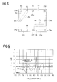
- Fig. 4 is a configuration diagram of a conductor pattern formed on the upper surface 14 of the piezoelectric substrate 12.
- Fig. 5 is a top view of a surface acoustic wave device. Figs. 4 and 5 correspond to Figs. 2 and 3 of the first embodiment, respectively.
- part of an interconnection line is formed on the piezoelectric substrate 12. That is, as shown in Fig. 4 , the input end 51 of the reception surface acoustic wave filter 50 is connected, using an interconnection line 53 disposed on the piezoelectric substrate 12, to a common antenna pad 41 connected to the transmission surface acoustic wave filter 60. As shown in Fig. 5 , the common antenna pad 41 is disposed immediately beneath the external electrode 28b connected to an antenna.
- Fig. 6 is a graph of the isolation characteristic.
- the heavy line represents the isolation characteristic of the surface acoustic wave device 10 according to the first embodiment.
- the thin line represents the isolation characteristic of a surface acoustic wave device 10 of the comparative example.
- the two surface acoustic wave devices have the same transmission frequency range of 824 to 849 MHz and the same reception frequency range of 869 to 894 MHz.
- the isolation characteristic of the first embodiment is improved as compared with that of the comparative example.
- a surface acoustic wave device has a structure substantially the same as that of the first embodiment.
- the second embodiment differs from the first embodiment in that part of an interconnection line (e.g., one half or more of the interconnection line) between the input end 51 of the reception surface acoustic wave filter 50 (see Fig. 2 ) and an antenna terminal (the external electrode 28b) is formed on a lower surface 34 of the cover 32, not the upper surface 33 of the cover 32.
- a conductor pattern corresponding to the conductor pattern 25v is formed on the lower surface 34 of the cover 32 in advance.
- the cover 32 is disposed so as to face the piezoelectric substrate 12.
- the cover 32 is then joined to the piezoelectric substrate 12 using the support layer 30.
- the capacitive coupling can be reduced.
- the isolation characteristic can be improved.
- FIG. 7 is a configuration diagram of a conductor pattern disposed on the upper surface 14 of the piezoelectric substrate 12.
- Fig. 7 corresponds to Fig. 2 of the first embodiment.
- a surface acoustic wave device has a structure substantially the same as that of the first embodiment.
- a reception surface acoustic wave filter 50 and a transmission surface acoustic wave filter 60 are disposed on the piezoelectric substrate 12.
- the surface acoustic wave device differs from that of the first embodiment in that the reception surface acoustic wave filter 50 and the transmission surface acoustic wave filter 60 are connected to the common antenna pad 41, and part of the interconnection line of the transmission surface acoustic wave filter 60 is disposed on the cover 32.
- the resonators 210 and 220 are connected to relay pads 65 and 66, respectively.
- the relay pad 65 is electrically connected to the relay pad 66 using a conductor pattern (not shown) formed on the upper surface 33 or the lower surface 34 of the cover 32.
- Signal lines of the transmission surface acoustic wave filter 60 are connected on the cover 32 and are separated on the piezoelectric substrate 12. In this way, the capacitive coupling between the interconnection lines can be reduced. Thus, the isolation characteristic can be improved.
- the interconnection line between the resonators 210 and 220 may be disposed on the lower surface 34 of the cover 32, and the interconnection line between the reception surface acoustic wave filter 50 and the common antenna pad 41 may be disposed on the upper surface 33 of the cover 32. Even in such a structure, the capacitive coupling between the signal lines can be reduced.
- FIG. 8 is a configuration diagram of a conductor pattern disposed on the upper surface 14 of the piezoelectric substrate 12.
- Fig. 8 corresponds to Fig. 2 of the first embodiment.
- a surface acoustic wave device has a structure substantially the same as that of the first embodiment.
- a reception surface acoustic wave filter 70 and a transmission surface acoustic wave filter 60 are disposed on the piezoelectric substrate 12.
- the surface acoustic wave device differs from that of the first embodiment in that the reception surface acoustic wave filter 70 and the transmission surface acoustic wave filter 60 are connected to the common antenna pad 41, and part of the interconnection line of the reception surface acoustic wave filter 70 is disposed on the cover 32.
- the reception surface acoustic wave filter 70 is of a ladder type.
- the reception surface acoustic wave filter 70 is a two-stage ladder filter.
- the reception surface acoustic wave filter 70 includes five resonators 310, 320, 330, 340, and 350.
- the resonators 310, 320, 330, 340, and 350 include IDTs 312, 322, 332, 342, and 352, respectively.
- Reflectors 314, 324, 334, 344, and 354 are disposed on both sides of the IDTs 312, 322, 332, 342, and 352, respectively.
- the resonators 310, 320, and 330 are connected in series between the common antenna pad 41 and a reception output pad 72.
- the resonator 320 is separated from the resonator 330 on the piezoelectric substrate 12.
- the resonators 320 and 330 are connected to relay pads 74 and 75, respectively.
- the relay pad 74 is electrically connected to the relay pad 75 using a conductor pattern disposed on the cover 32.
- the resonator 340 is connected in parallel between the neighboring resonators 310 and 320, and the resonator 350 is connected in parallel between the resonators 320 and 330. That is, one end of the resonator 340 is connected to the connection point between the series-connected resonators 310 and 320. The other end of the resonator 340 is connected to an earth pad 78. One end of the resonator 350 is connected to the connection point between the series-connected resonators 320 and 330. The other end of the resonator 350 is connected to the earth pad 78.
- part of the interconnection line between the resonators 320 and 330 is disposed on the cover 32.
- capacitive coupling between the interconnection lines can be reduced as compared with the case where the entirety of the interconnection line between the resonators 320 and 330 is disposed on the piezoelectric substrate 12. Therefore, the isolation can be improved.
- the isolation can be improved even when part of the interconnection line between the resonators 310 and 320 is disposed on the cover 32 instead of the interconnection line between the resonators 320 and 330, the isolation can be improved.
- the interconnection line between the resonators 320 and 330 tends to be easily affected by noise on the transmission side caused by attenuation of a reception signal.
- the surface acoustic wave devices 10x to 10z according to the fifth embodiment have a structure similar to that of the first embodiment.
- Each of the surface acoustic wave devices 10x to 10z includes a piezoelectric substrate 12, a support layer 30, a reinforcing resin 36, and an external electrode 28.
- the fifth embodiment differs from the first embodiment in that each of the surface acoustic wave devices 10x to 10z is a filter including only a pair of surface acoustic wave filters 80.
- the acoustic wave filters 80 and pads 41, 64, 65, 66, and 68 are formed on an upper surface 14 of the piezoelectric substrate 12.
- the acoustic wave filter 80 is a three-stage ladder filter including seven resonators 210, 220, 230, 240, 250, 260, and 270.
- each of the surface acoustic wave devices 10x to 10z four external electrodes 28p to 28s serving as the external electrodes 28 are provided on an upper surface 11 (see Fig. 11 ) of each of the surface acoustic wave devices 10x to 10z.
- the external electrode 28r serves as an input terminal.
- the external electrode 28p serves as an output terminal.
- the external electrodes 28q and 28s serve as GND terminals.
- conductor patterns 25q, 25r, and 25s and one of conductor patterns 25x, 25y, and 25z are formed on the upper surface 33 or the lower surface 34 (see Fig. 11 ) of the cover 32.
- the conductor pattern 25q is part of an interconnection line that electrically connects the external electrode 28q to the pad 68.
- the conductor pattern 25r is part of an interconnection line that electrically connects the external electrode 28r to the pad 64.
- the conductor pattern 25s is part of an interconnection line that electrically connects the external electrode 28s to the pad 68.
- each of the conductor patterns 25x, 25y, and 25z is part of an interconnection line (a cover interconnection line) that electrically connects the pad 65 to the pad 66.
- the conductor pattern 25x is provided on the upper surface 33 of the cover 32, the conductor pattern 25x is formed, together with the conductor patterns 25q to 25s (see Fig. 10 ), by plating. Subsequently, the conductor pattern 25x is connected to a conductor pattern 24x (a via interconnection line) that passes through the support layer 30 and the cover 32.
- the support layer 30 is formed by using a photosensitive resin first. Thereafter, a through-hole is formed in the support layer 30 by a laser process. Subsequently, a conductive pattern 24y or 24z (a via interconnection line) is formed by, for example, plating.
- a conductor pattern serving as the conductor pattern 25y is formed on a surface serving as the lower surface 34 of a resin sheet member serving as the cover 32 in advance. Subsequently, a resin sheet member serving as the cover 32 is bonded onto the support layer 30. At that time, the conductor pattern 25y is connected to the conductive pattern 24y that passes through the support layer 30.
- a conductor pattern serving as the conductor pattern 25z is formed on an upper surface of the support layer 30. At that time, the conductor pattern 25z is connected to the conductive pattern 24z that passes through the support layer 30. Subsequently, a resin sheet member serving as the cover 32 is bonded onto the support layer 30.
- one of the conductor patterns 25x, 25y, and 25z (cover interconnection lines) is disposed on the upper surface 33 or the lower surface 34 of the cover 32.
- the pad 65 is connected to the pad 66 using an interconnection line partially extending on the cover 32.
- capacitive coupling between interconnection lines can be reduced as compared with the case where the connection point between the resonators 220 and 250 is connected to the resonator 210 using only an interconnection line disposed on the piezoelectric substrate 12.
- the VSWR of a filter can be improved.
- part of an interconnection line used for longitudinally connecting two longitudinally coupled resonator type surface acoustic wave filters to each other can be disposed on the cover.
- capacitive coupling between interconnection lines can be reduced as compared with the case where two longitudinally coupled resonator type surface acoustic wave filters are connected to each other using only an interconnection line disposed on the piezoelectric substrate,
- the VSWR of a filter can be improved.
- a surface acoustic wave element functions as a surface acoustic wave resonator or a longitudinally coupled resonator type surface acoustic wave filter.
- Boundary acoustic wave devices according to sixth to tenth embodiments are described next.
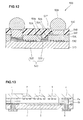
- a boundary acoustic wave device 500 according to a sixth embodiment is described with reference to Fig. 12 .
- the boundary acoustic wave device 500 includes a piezoelectric substrate 510 made of LiNbO 3 and a Au conductor pattern 520 formed on an upper surface 512 of the piezoelectric substrate 510.
- the conductor pattern 520 includes an IDT 522 and a pad 523.
- a adhesive layer 524 made of Ti is formed on the pad 523.
- a support layer 530 made of SiO 2 is formed on the upper surface 512 of the piezoelectric substrate 510 and the conductor pattern 520. The support layer 530 is partially removed using a photolithography technique so that the adhesive layer 524 of the pad 523 is exposed. Thus, a via (a through-hole) 534 is formed.
- a support layer interconnection line 526 is formed on an upper surface 532 of the support layer 530, and a via interconnection line 525 is formed in the via 534 by, for example, plating.
- One end of the support layer interconnection line 526 is connected to the adhesive layer 24 of the pad 523 using the via interconnection line 525 that passes through the support layer 530.
- a cover 540 is formed on the upper surface 532 of the support layer 530 and the support layer interconnection line 526.
- the cover 540 is made from a sound absorbing material, such as an epoxy resin, in order to attenuate vibration in a spurious mode that propagates in the support layer 530.
- the cover 540 is partially removed by sandblasting. Removed portions of the cover 540 are filled with an under bump metal 527 by plating. A solder bump 528 is formed on the under bump metal 527. The solder bump 528 serves as an external electrode protruding from an upper surface 542 of the cover 540.
- the boundary acoustic wave device 500 converts boundary acoustic waves into an electrical signal using boundary acoustic waves propagating at a boundary between the piezoelectric substrate 510 made of LiNbO 3 , which is a first medium, and the support layer 530 made of SiO 2 , which is a second medium.
- the surface acoustic wave device requires the vibration space 16 around the IDT 22.
- the IDT 522 is disposed on an interface between the piezoelectric substrate 510 and the support layer 530. Thus, a vibration space is not required around the IDT 522.
- the boundary acoustic wave device 500 serves as a duplexer.
- a method for designing an IDT electrode that is the same as that for the surface acoustic wave device 10 of the first embodiment can be applied to the boundary acoustic wave device 500. That is, conductor patterns similar to those of Fig. 2 are formed on the upper surface 512 of the piezoelectric substrate 510. Thus, a reception surface acoustic wave filter 50, a transmission surface acoustic wave filter 60, and seven pads 52, 54, 56, 58, 62, 64, and 68 are formed.
- the filters 50 and 60 shown in Fig. 2 are boundary acoustic wave filters.
- the reception surface acoustic wave filter 50 is a boundary acoustic wave filter of a balanced type.
- the arrangement of the interconnection lines is also similar to that of the first embodiment. Part of an interconnection line between the input end 51 (see Fig. 2 ) of the reception filter 50 and an antenna terminal serving as an external electrode is formed on the upper surface 532 of the support layer 530. That is, part of the interconnection line is formed from the support layer interconnection line 526.
- LiTaO 3 and LiNbO 3 used for the piezoelectric substrate 510 of the boundary acoustic wave device 500 have a relative permittivity as high as about 40 to 50. Accordingly, in the one-chip boundary acoustic wave device 500, if interconnection lines are disposed on the piezoelectric substrate 510, the capacitive coupling between the interconnection lines is increased. In particular, as the chip is made smaller using a wafer-level chip-size packaging technology, the effect of the capacitive coupling increases. Thus, the isolation characteristic deteriorates.
- the support layer 530 of the boundary acoustic wave device 500 is formed from SiO 2 having a relative permittivity of 3 to 5.
- part of an interconnection line between the input end 51 of the reception filter 50 (see Fig. 2 ) and the antenna terminal serving as an external electrode is disposed on the upper surface 532 of the support layer 530.
- the part of an interconnection line between the input end 51 (see Fig. 2 ) of the reception filter 50 and the antenna terminal serving as an external electrode is disposed on the piezoelectric substrate 510, if part of an interconnection line is disposed on the support layer 530 formed from a dielectric material having a low relative permittivity, an increase in the capacitive coupling between interconnection lines can be prevented. Accordingly, even when the chip is made smaller, the isolation characteristic can be improved.
- a boundary acoustic wave device has a structure substantially the same as that of the sixth embodiment.
- the arrangement of interconnection lines of the seventh embodiment differs from that of the sixth embodiment. That is, the seventh embodiment differs from the sixth embodiment only in the following point: part of an interconnection line between the input end 51 (see Fig. 2 ) of the reception filter 50 and the antenna terminal serving as an external electrode is disposed on the upper surface 542 of the cover 540, not on the upper surface 532 of the support layer 530.
- the capacitive coupling between interconnection lines can be reduced, and therefore, the isolation characteristic can be improved.
- a boundary acoustic wave device has a structure substantially the same as that of the sixth embodiment.
- conductor patterns disposed on the upper surface 512 of the piezoelectric substrate 510 are formed in the same manner as in the surface acoustic wave device of the third embodiment.
- the interconnection lines are arranged in the same manner as in the third embodiment.
- conductor patterns are formed on the upper surface 512 of the piezoelectric substrate 510 so that an interconnection line between the resonators 210 and 220 is separated, and the resonators 210 and 220 are connected to the relay pads 65 and 66, respectively.
- the filters 50 and 60 shown in Fig. 7 are boundary acoustic wave filters.
- the resonators 210, 220, 230, and 240 of the transmission filter 50 are boundary acoustic wave resonators.
- the relay pad 65 is electrically connected to the relay pad 66 using a via interconnection line 525 that passes through the support layer 530 and the support layer interconnection line 526 formed on the upper surface 532 of the support layer 530.
- the capacitive coupling between interconnection lines can be reduced, and therefore, the isolation characteristic can be improved.
- the interconnection line between the resonators 210 and 220 may be disposed on the upper surface 542 of the cover 540, and the interconnection line between the reception filter 50 and the common antenna pad 41 may be disposed on the upper surface 542 of the cover 540. Even in such a structure, the capacitive coupling between the signal lines can be reduced.
- a boundary acoustic wave device has a structure substantially the same as that of the sixth embodiment.
- conductor patterns are formed on the upper surface 512 of the piezoelectric substrate 510 in the same manner as in the surface acoustic wave device of the fourth embodiment.
- the interconnection lines are arranged in the same manner as in the fourth embodiment.
- conductor patterns are formed on the upper surface 512 of the piezoelectric substrate 510 so that a reception filter 70 and a transmission filter 60 are connected to a common antenna pad 41, and part of an interconnection line of the reception filter 70 is disposed on the support layer 530. That is, the reception filter 70 is a ladder filter. An interconnection line between the resonators 320 and 330 of the reception filter 70 is separated, and the resonators 320 and 330 are connected to the relay pads 74 and 75, respectively.
- the relay pad 74 is electrically connected to the relay pad 75 using a via interconnection line 525 that passes through the support layer 530 and a support layer interconnection line 526 formed on the upper surface 532 of the support layer 530.
- the filters 60 and 70 are boundary acoustic wave filters
- the resonators 210, 220, 230, 240, 310, 320, 330, 340, and 350 are boundary acoustic wave resonators.
- part of an interconnection line between the resonators 320 and 330 is disposed on the support layer 530. Accordingly, the capacitive coupling between the interconnection lines can be reduced, and therefore, the isolation can be improved, as compared with the case where the entirety of the interconnection line between the resonators 320 and 330 is disposed on the piezoelectric substrate 510.
- the isolation characteristic can be improved even when part of the interconnection line between the resonators 310 and 320 is disposed on the support layer 530 in place of part of the interconnection line between the resonators 320 and 330.
- the interconnection line between the resonator 320 and 330 tends to be easily affected by noise on the transmission side caused by attenuation of a reception signal.
- a boundary acoustic wave device has a structure substantially the same as that of the sixth embodiment.
- conductor patterns are formed on the upper surface 512 of the piezoelectric substrate 510 in the same manner as in the surface acoustic wave device of the fifth embodiment.
- the interconnection lines are arranged in the same manner as in the fifth embodiment.
- the boundary acoustic wave device is a filter including only a pair of filters 80 and a three-stage ladder filter including seven resonators 210, 220, 230, 240, 250, 260, and 270.
- the filter 80 shown in Fig. 9 is a boundary acoustic wave filter
- the resonators 210, 220, 230, and 240 are boundary acoustic wave resonators.
- the arrangement of the interconnection lines is similar to that of the fifth embodiment. That is, part of an interconnection line that electrically connects the pad 65 to the pad 66 is disposed on the upper surface 532 of the support layer 530.
- the pad 65 is connected to the pad 66 using an interconnection line that passes through the support layer 530 (a via interconnection line 525 passing through the support layer and a support layer interconnection line 526 disposed on the support layer 530). Accordingly, the capacitive coupling between the interconnection lines can be reduced, and therefore, the VSWR of the filter can be increased, as compared with the case where an interconnection point between the resonators 220 and 250 is connected to the resonator 210 using only an interconnection line disposed on the piezoelectric substrate 510.
- part of the interconnection line cascade connecting two longitudinally coupled resonator type filters to each other may be disposed on the upper surface 532 of the support layer 530. Even in such a case, capacitive coupling between the interconnection lines can be reduced, and therefore, the VSWR of the filter can be improved, as compared with the case of cascade connecting two longitudinally coupled resonator type filters by only an interconnection line disposed on the piezoelectric substrate 510.
- the boundary acoustic wave element is a boundary acoustic wave resonator or a longitudinally coupled resonator type filter.
- the isolation can be improved.
- the VSWR of the filter can be improved.
- the isolation can be improved.
- the VSWR of the filter can be improved.
- the structures of the reception surface acoustic wave filter and the transmission surface acoustic wave filter are not limited to those of the above-described embodiments.
- the reflectors of the surface acoustic wave resonators may be omitted.
- the structures of the reception boundary acoustic wave filter and the transmission boundary acoustic wave filter are not limited to those of the above-described embodiments.
- the reflectors of the boundary acoustic wave resonators may be omitted.
- the surface acoustic wave device may have a structure not including the reinforcing resin 36.
- the interconnection line (the conductor pattern 25) disposed on the cover 32 is provided on a major surface facing the piezoelectric substrate 12 (the lower surface 34).
Landscapes
- Physics & Mathematics (AREA)
- Acoustics & Sound (AREA)
- Surface Acoustic Wave Elements And Circuit Networks Thereof (AREA)
Abstract
Description
- The present invention relates to a surface acoustic wave device and a boundary acoustic wave device.
- In recent years, a wafer-level chip-size packaging (WLCSP) technology has been developed that can reduce the size of a package of a surface acoustic wave device, such as a surface acoustic wave filter, and a boundary acoustic wave device, such as a boundary acoustic wave filter, to a component chip size.
- For example, as shown in
Fig. 13 , a surface acoustic wave device includes apiezoelectric substrate 1 and aresin substrate 7 that faces thepiezoelectric substrate 1. Thepiezoelectric substrate 1 includes a conductor pattern having an IDT (a comb-shaped electrode) 2, areflector 3, and apad 4 formed thereon. Theresin substrate 7 includes anexternal electrode 8. Thepiezoelectric substrate 1. and theresin substrate 7 are bonded and sealed by lightcurable resins pad 4 is electrically connected to the external electrode 8 (refer to, for example, Patent Document 1). - [Patent Document 1] Japanese Unexamined Patent Application Publication No.
2003-37471 - When such a structure in which a piezoelectric substrate is covered and sealed by a cover is applied to surface acoustic wave devices and boundary acoustic wave devices, capacitive coupling tends to increase. In particular, when the sizes of the devices are reduced by employing a wafer-level chip-size packaging (WLCSP) structure, the capacitive coupling significantly increases. An increasing capacitive coupling deteriorates the isolation characteristics and VSWR.
- Accordingly, the present invention provides a surface acoustic wave device and a boundary acoustic wave device that can reduce capacitive coupling between signal lines.
- To solve the above-described problem, the present invention provides a surface acoustic wave device having the following structure.
- A surface acoustic wave device includes a piezoelectric substrate, a cover joined to the piezoelectric substrate with a support layer therebetween and with a spacing kept therebetween, and a transmission surface acoustic wave filter and a reception surface acoustic wave filter formed on a major surface of the piezoelectric substrate adjacent to the cover and inside the support layer. External electrodes are provided on the side of the cover opposite that facing the piezoelectric substrate. The external electrodes include an antenna terminal electrically connected to the transmission surface acoustic wave filter and the reception surface acoustic wave filter, a transmission input terminal electrically connected to the transmission surface acoustic wave filter, and a reception output terminal electrically connected to the reception surface acoustic wave filter The reception surface acoustic wave filter is electrically connected to the antenna terminal using an interconnection line, and the interconnection line includes (a) a piezoelectric substrate line formed on the piezoelectric substrate, (b) a cover line disposed on one of an upper surface and a lower surface of the cover, and (c) a via line that passes through the support layer and the cover so as to connect one end of the piezoelectric substrate line to one end of the cover line,
- Such a structure can reduce capacitive coupling between signal lines by reducing the length of the piezoelectric line or separating the piezoelectric line disposed on the piezoelectric substrate of the interconnection line used for electrically connecting the reception surface acoustic wave filter to the antenna terminal using the cover line and the via line.
- Preferably, the reception surface acoustic wave filter is a balanced surface acoustic wave filter including one unbalanced signal terminal to which an unbalanced signal is input and two balanced signal terminals that output balanced signals, and the antenna terminal is electrically connected to the unbalanced signal terminal. The reception output terminal is electrically connected to the balanced signal terminals.
- Such a structure can provide a balanced surface acoustic wave filter having, in particular, an excellent balanced characteristic.
- Note that the reception output terminal may be a pair of external electrodes, each connected to a corresponding one of the two balanced signal terminals of the balanced filter.
- To solve the above-described problem, the present invention further provides a surface acoustic wave device having the following structure.
- A surface acoustic wave device includes a piezoelectric substrate, a cover joined to the piezoelectric substrate with a support layer therebetween and with a spacing kept therebetween, and a transmission surface acoustic wave filter and a reception surface acoustic wave filter formed on a major surface of the piezoelectric substrate adjacent to the cover and inside the support layer. External electrodes are provided on the side of the cover opposite that facing the piezoelectric substrate. The external electrodes include an antenna terminal electrically connected to the transmission surface acoustic wave filter and the reception surface acoustic wave filter, a transmission input terminal electrically connected to the transmission surface acoustic wave filter, and a reception output terminal electrically connected to the reception surface acoustic wave filter. The transmission surface acoustic wave filter includes a plurality of series-connected surface acoustic wave resonators. An interconnection line that electrically connects at least one pair of the neighboring series-connected surface acoustic wave resonators includes (a) at least one cover line disposed on one of an upper surface and a lower surface of the cover and (b) at least one pair of via lines that passes through at least the support layer so as to connect the at least one cover line to one of the at least one pair of the neighboring series-connected surface acoustic wave resonators and the other surface acoustic wave resonator.
- Such a structure can reduce capacitive coupling between signal lines by removing a line disposed on the piezoelectric substrate of the interconnection line used for electrically connecting the at least one pair of neighboring series-connected surface acoustic wave resonators of the transmission surface acoustic wave filter using the cover line and the via line, by reducing the length of the line disposed on the piezoelectric substrate, or by separating the line disposed on the piezoelectric substrate.
- To solve the above-described problem, the present invention further provides a surface acoustic wave device having the following structure.
- A surface acoustic wave device includes a piezoelectric substrate, a cover joined to the piezoelectric substrate with a support layer therebetween and with a spacing kept therebetween, and a transmission surface acoustic wave filter and a reception surface acoustic wave filter formed on a major surface of the piezoelectric substrate adjacent to the cover and inside the support layer. External electrodes are provided on the side of the cover opposite that facing the piezoelectric substrate. The external electrodes include an antenna terminal electrically connected to the transmission surface acoustic wave filter and the reception surface acoustic wave filter, a transmission input terminal electrically connected to the transmission surface acoustic wave filter, and a reception output terminal electrically connected to the reception surface acoustic wave filter. The reception surface acoustic wave filter includes a plurality of series-connected surface acoustic wave resonators. An interconnection line that electrically connects at least one pair of the neighboring series-connected surface acoustic wave resonators includes (a) at least one cover line disposed on one of an upper surface and a lower surface of the cover and (b) at least one pair of via lines that passes through at least the support layer so as to connect the at least one cover line to one of the at least one pair of the neighboring series-connected surface acoustic wave resonators and the other surface acoustic wave resonator.
- Such a structure can reduce capacitive coupling between signal lines by removing a line disposed on the piezoelectric substrate of the interconnection line used for electrically connecting the at least one pair of neighboring series-connected surface acoustic wave resonators of the reception surface acoustic wave filter, by reducing the length of the line disposed on the piezoelectric substrate, or by separating the line disposed on the piezoelectric substrate.
- Note that at least one pair of neighboring series-connected surface acoustic wave resonators of the reception surface acoustic wave filter may be a longitudinally coupled resonator type surface acoustic wave filter including three IDTs and a surface acoustic wave resonator including one IDT.
- To solve the above-described problem, the present invention further provides a surface acoustic wave device having the following structure.
- A surface acoustic wave device includes a piezoelectric substrate, a cover joined to the piezoelectric substrate with a support layer therebetween and with a spacing kept therebetween, a surface acoustic wave filter formed on a major surface of the piezoelectric substrate adjacent to the cover and inside the support layer, and external terminals provided on the side of the cover opposite that facing the piezoelectric substrate. The external terminals include an input terminal and an output terminal electrically connected to the surface acoustic wave filter. The surface acoustic wave filter includes a plurality of series-connected surface acoustic wave elements. An interconnection line that electrically connects at least one pair of the neighboring series-connected surface acoustic wave elements includes (a) at least one cover line disposed on one of an upper surface and a lower surface of the cover and (b) at least one pair of via lines that passes through at least the support layer so as to connect the at least one cover line to one of the at least one pair of the neighboring series-connected surface acoustic wave elements and the other surface acoustic wave element.
- Such a structure can reduce capacitive coupling between signal lines.
- Preferably, in the above-described structures, the cover is disposed inside a peripheral portion of the piezoelectric substrate when viewed in a direction perpendicular to the major surface of the piezoelectric substrate, and the surface acoustic wave device further includes a reinforcing resin that covers the entirety of a portion from the major surface of the cover remote from the piezoelectric substrate to the peripheral portion of the major surface of the piezoelectric substrate.
- Such a structure can seal the reception surface acoustic wave filter and the transmission surface acoustic wave filter with the reinforcing resin. Accordingly, a sufficient resistance to moisture can be obtained. Thus, for example, after the surface acoustic wave device is mounted on a circuit board, the need for covering the surface acoustic wave device with a resin can be eliminated.
- Preferably, the cover line is formed by plating.
- To solve the above-described problem, the present invention further provides a boundary acoustic device having the following structure.
- A boundary acoustic wave device includes a piezoelectric substrate, a cover joined to the piezoelectric substrate with a support layer therebetween, a transmission boundary acoustic wave filter and a reception boundary acoustic wave filter formed at an interface between the piezoelectric substrate and the support layer, and external electrodes provided on the side of the cover opposite that facing the piezoelectric substrate. The external electrodes include an antenna terminal electrically connected to the transmission boundary acoustic wave filter and the reception boundary acoustic wave filter, a transmission input terminal electrically connected to the transmission boundary acoustic wave filter, and a reception output terminal electrically connected to the reception boundary acoustic wave filter. The reception boundary acoustic wave filter is electrically connected to the antenna terminal using an interconnection line, and the interconnection line includes (a) a piezoelectric substrate line formed on the piezoelectric substrate, (b) a support layer line disposed on an upper surface of the cover, and (c) a via line that passes through the support layer so as to connect one end of the piezoelectric substrate line to one end of the support layer line.
- Such a structure can reduce capacitive coupling between signal lines by reducing the length of the piezoelectric line or separating the piezoelectric line disposed on the piezoelectric substrate of the interconnection line used for electrically connecting the reception boundary acoustic wave filter to the antenna terminal using the cover line and the via line.
- Preferably, the reception boundary acoustic wave filter is a balanced boundary acoustic wave filter including one unbalanced signal terminal to which an unbalanced signal is input and two balanced signal terminals that output balanced signals, and the antenna terminal is electrically connected to the unbalanced signal terminal. The reception output terminal is electrically connected to the balanced signal terminals.
- Such a structure can provide a balanced boundary acoustic wave filter having, in particular, an excellent balanced characteristic.
- Note that the reception output terminal may be a pair of external electrodes, each connected to a corresponding one of the two balanced signal terminals of the balanced filter.
- To solve the above-described problem, the present invention further provides a boundary acoustic wave device having the following structure.
- A boundary acoustic wave device includes a piezoelectric substrate, a cover joined to the piezoelectric substrate with a support layer therebetween, a transmission boundary acoustic wave filter and a reception boundary acoustic wave filter formed at an interface between the piezoelectric substrate and the support layer, and external electrodes provided on the side of the cover opposite that facing the piezoelectric substrate. The external electrodes include an antenna terminal electrically connected to the transmission boundary acoustic wave filter and the reception boundary acoustic wave filter, a transmission input terminal electrically connected to the transmission boundary acoustic wave filter, and a reception output terminal electrically connected to the reception boundary acoustic wave filter. The transmission boundary acoustic wave filter includes a plurality of series-connected boundary acoustic wave resonators. An interconnection line that electrically connects at least one pair of the neighboring series-connected boundary acoustic wave resonators includes (a) at least one support layer line disposed on an upper surface of the support layer and (b) at least one pair of via lines that passes through at least the support layer so as to connect the at least one support layer line to one of the at least one pair of the neighboring series-connected boundary acoustic wave resonators and the other boundary acoustic wave resonator.
- Such a structure can reduce capacitive coupling between signal lines by removing a line disposed on the piezoelectric substrate of the interconnection line used for electrically connecting the at least one pair of neighboring series-connected boundary acoustic wave resonators of the transmission boundary acoustic wave filter using the cover line and the via line, by reducing the length of the line disposed on the piezoelectric substrate, or by separating the line disposed on the piezoelectric substrate.
- To solve the above-described problem, the present invention further provides a boundary acoustic wave device having the following structure.
- A boundary acoustic wave device includes a piezoelectric substrate, a cover joined to the piezoelectric substrate with a support layer therebetween, a transmission boundary acoustic wave filter and a reception boundary acoustic wave filter formed at an interface between the piezoelectric substrate and the support layer, and external electrodes provided on the side of the cover opposite that facing the piezoelectric substrate. The external electrodes include an antenna terminal electrically connected to the transmission boundary acoustic wave filter and the reception boundary acoustic wave filter, a transmission input terminal electrically connected to the transmission boundary acoustic wave filter, and a reception output terminal electrically connected to the reception boundary acoustic wave filter The reception boundary acoustic wave filter includes a plurality of series-connected boundary acoustic wave resonators. An interconnection line that electrically connects at least one pair of the neighboring series-connected boundary acoustic wave resonators includes (a) at least one support layer line disposed on an upper surface of the cover and (b) at least one pair of via lines that passes through at least the support layer so as to connect the at least one support layer line to one of the at least one pair of the neighboring series-connected boundary acoustic wave resonators and the other boundary acoustic wave resonator.
- Such a structure can reduce capacitive coupling between signal lines by removing a line disposed on the piezoelectric substrate of the interconnection line used for electrically connecting the at least one pair of neighboring series-connected boundary acoustic wave resonators of the reception boundary acoustic wave filter, by reducing the length of the line disposed on the piezoelectric substrate, or by separating the line disposed on the piezoelectric substrate.
- Note that at least one pair of neighboring series-connected boundary acoustic wave resonators of the reception boundary acoustic wave filter may be a longitudinally coupled resonator type boundary acoustic wave filter including three IDTs and a boundary acoustic wave resonator including one IDT.
- To solve the above-described problem, the present invention further provides a boundary acoustic wave device having the following structure.
- A boundary acoustic wave device includes a piezoelectric substrate, a cover joined to the piezoelectric substrate with a support layer therebetween, a boundary acoustic wave filter formed at an interface between the piezoelectric substrate and the support layer, and external terminals provided on the side of the cover opposite that facing the piezoelectric substrate. The external terminals include an input terminal and an output terminal electrically connected to the boundary acoustic wave filter. The boundary acoustic wave filter includes a plurality of series-connected boundary acoustic wave elements. An interconnection line that electrically connects at least one pair of the neighboring series-connected boundary acoustic wave elements includes (a) at least one support layer line disposed on an upper surface of the cover and (b) at least one pair of via lines that passes through at least the support layer so as to connect the at least one support layer line to one of the at least one pair of the neighboring series-connected boundary acoustic wave elements and the other boundary acoustic wave element.
- Such a structure can reduce capacitive coupling between signal interconnection lines.
- Preferably, the support layer line is formed by plating.
- According to the present invention, capacitive coupling between interconnection lines of a surface acoustic wave device or a boundary acoustic wave device can be reduced.
-
- [
Fig. 1] Fig. 1 is a cross-sectional view of a surface acoustic wave device (a first embodiment). - [
Fig. 2] Fig. 2 is a configuration diagram of conductor patterns disposed on a piezoelectric substrate (the first embodiment). - [
Fig. 3] Fig. 3 is a top view of the surface acoustic wave device (the first embodiment). - [
Fig. 4] Fig. 4 is a configuration diagram of conductor patterns disposed on a piezoelectric substrate (a comparative example). - [
Fig. 5] Fig. 5 is a top view of a surface acoustic wave device (the comparative example). - [
Fig. 6] Fig. 6 is a graph illustrating the isolation characteristics (the first embodiment and the comparative example). - [
Fig. 7] Fig. 7 is a configuration diagram of conductor patterns disposed on a piezoelectric substrate (a third embodiment). - [
Fig. 8] Fig. 8 is a configuration diagram of conductor patterns disposed on a piezoelectric substrate (a fourth embodiment). - [
Fig. 9] Fig. 9 is a configuration diagram of conductor patterns disposed on a piezoelectric substrate (a fifth embodiment). - [
Fig. 10] Fig. 10 is a top view of the surface acoustic wave device (the fifth embodiments). - [
Fig. 11] Fig. 11 is a cross-sectional view of the surface acoustic wave device (the fifth embodiment). - [
Fig. 12] Fig. 12 is a cross-sectional view of a boundary acoustic wave device (a sixth embodiment). - [
Fig. 13] Fig. 13 is a cross-sectional view of a surface acoustic wave device (a prior art). -
- 10, 10x, 10y, 10z
- surface acoustic wave device
- 12
- piezoelectric substrate
- 24, 24x, 24y, 24z
- via interconnection line
- 25, 25x, 25y, 25z
- cover interconnection line
- 28, 28a - 28h
- external electrode
- 30
- support layer
- 32
- cover
- 50
- reception surface acoustic wave filter
- 60
- transmission surface acoustic wave filter
- 70
- reception surface acoustic wave filter
- 80
- surface acoustic wave filter
- 500
- boundary acoustic wave device
- 510
- piezoelectric substrate
- 525
- via interconnection line
- 526
- support layer interconnection line
- 530
- support layer
- 540
- cover
- Embodiments of the present invention are described with reference to
Figs. 1 to 12 . - First, surface acoustic wave devices according to first to fifth embodiments are described with reference to
Figs. 1 to 11 . - A surface
acoustic wave device 10 according to a first embodiment is described with reference toFigs. 1 to 6 . - As shown in a cross-sectional view of
Fig. 1 , the surfaceacoustic wave device 10 includes aconductive pattern 20 formed on anupper surface 14 which is one of two major surfaces of apiezoelectric substrate 12. Theconductive pattern 20 includes anIDT 22 and apad 23. Acover 32 is disposed so as to face theupper surface 14 with asupport layer 30 therebetween. Avibration space 16 is formed around theIDT 22. That is, theIDT 22 is disposed inside thesupport layer 30. Thus, surface acoustic waves can freely propagate in a portion of thepiezoelectric substrate 12 adjacent to thevibration space 16. Thesupport layer 30 is formed inside aperipheral portion 15 of theupper surface 14 of thepiezoelectric substrate 12. - In addition, a reinforcing
resin 36 entirely covers a portion from anupper surface 33 of thecover 32 to theperipheral portion 15 of theupper surface 14 of thepiezoelectric substrate 12. Anexternal electrode 28 is exposed through the reinforcingresin 36 so that the surfaceacoustic wave device 10 can be mounted on a circuit board of an electronic device. - Through-holes are formed in the
cover 32 and the reinforcingresin 36.Conductor patterns pad 23 is connected to theexternal electrode 28. Theconductor patterns conductor pattern 25 formed on theupper surface 33 of thecover 32. Alternatively, although not shown, theconductor patterns conductor patterns - The reinforcing
resin 36 extends along the entire peripheral edge of theupper surface 14 of thepiezoelectric substrate 12 of the surfaceacoustic wave device 10. Thus, the reinforcingresin 36 seals theupper surface 14 of thepiezoelectric substrate 12. In this way, thevibration space 16 is sealed and blocked from the external environment. - A plurality of the surface
acoustic wave devices 10 can be produced at the same time in the form of a substrate assembly. For example, theconductive pattern 20 is formed on theupper surface 14 of a wafer (a substrate assembly) made of one of LiTaO3 and LiNbO3 for thepiezoelectric substrate 12 by, for example, vapor deposition of a metal film. Thereafter, thesupport layer 30 is formed using a photosensitive resin. A resin sheet member that serves as thecover 32 is then bonded onto thesupport layer 30. Subsequently, the sheet member is cut into pieces, each serving as the surfaceacoustic wave device 10 by, for example, a laser process. After through-holes are formed in the sheet member and thesupport layer 30 so as to reach thepad 23, the conductor pattern 24 (a via interconnect line) is formed by plating. Furthermore, after theconductor pattern 25 is formed on theupper surface 33 of thecover 32 by plating, the reinforcingresin 36 is applied to theupper surface 14 of the wafer. Subsequently, a through-hole is formed in the reinforcingresin 36. When a photosensitive resin is used for the reinforcing resin, the through-hole is formed by a lithographic technique. In contrast, when a non-photosensitive resin is used for the reinforcing resin, the through-hole is formed by a laser process. Theconductor pattern 26 is then formed in the through-hole formed in the reinforcingresin 36 by plating. Furthermore, theexternal electrodes 28 are formed by plating. Finally, the wafer is divided into pieces, each serving as the surfaceacoustic wave device 10. - The surface
acoustic wave device 10 functions as a duplexer. As schematically shown inFig. 2 , a reception surfaceacoustic wave filter 50, a transmission surfaceacoustic wave filter 60, and sevenpads upper surface 14 of thepiezoelectric substrate 12. - The reception surface
acoustic wave filter 50 functions as a balanced filter having a balanced-unbalanced conversion function. The reception surfaceacoustic wave filter 50 includes tworesonators IDTs IDTs IDTs IDTs - More specifically, one end of the
resonator 100 and one end of theresonator 110 are connected to thereception antenna pad 52 in parallel. TheIDTs resonator 100 and the other end of theresonator 110, respectively. Theresonators resonators - The longitudinally coupled resonator type surface acoustic wave filters 140 and 150 are longitudinally connected to the longitudinally coupled resonator type surface acoustic wave filters 120 and 130, respectively. Balanced signals having phases about 180 degrees different from each other are output from the
balanced signal pads IDTs - The earth interconnection line (shown by a heavy line in the drawing) connected to the
earth pad 58 is formed on theupper surface 14 of thepiezoelectric substrate 12 and insulatinglayers - Note that a reflector (not shown) may be provided in the
resonators - The transmission surface
acoustic wave filter 60 is a three-stage ladder filter. The transmission surfaceacoustic wave filter 60 includes sevenresonators resonators IDTs Reflectors IDTs - The
resonators transmission input pad 64 to which a transmission signal is input and thetransmission antenna pad 62 connected to an antenna. - The
resonators resonators resonators resonators resonator 250 is connected to the connection point between the series-connectedresonators resonator 250 is connected to theearth pad 68. One end of theresonator 260 is connected to the connection point between the series-connectedresonators resonator 260 is connected to theearth pad 68. One end of theresonator 270 is connected to the connection point between the series-connectedresonators resonator 270 is connected to theearth pad 68. - As shown by a plan view given in
Fig. 3 , eightexternal electrodes 28a to 28h serving as the external electrodes 28 (seeFig. 1 ) are provided on anupper surface 11 of the surface acoustic wave device 10 (seeFig. 1 ).Conductor patterns 25a to 25e and a conductor pattern 25v shown by dotted lines are formed on anupper surface 33 of thecover 32 so as to serve as the conductor pattern 25 (seeFig. 1 ). Theconductor patterns 25a to 25e, the conductor pattern 25v, and theconductor patterns external electrodes 28a to 28h to thepads - The
external electrode 28b serves as an antenna terminal connected to thereception antenna pad 52 of the reception surfaceacoustic wave filter 50 and thetransmission antenna pad 62 of thetransmission filter 60. Theexternal electrode 28e is connected to thetransmission input pad 64 of the transmission surfaceacoustic wave filter 60 and serves as a transmission input terminal. Theexternal electrode 28g is connected to thebalanced signal pad 56 serving as a balanced signal terminal of the reception surfaceacoustic wave filter 50. Theexternal electrode 28h is connected to thebalanced signal pad 54 serving as a balanced signal terminal of the reception surfaceacoustic wave filter 50. Theexternal electrodes - The conductor pattern 25v is part of interconnection line between an
input end 51 of the reception surface acoustic wave filter 50 (seeFig. 2 ) and the antenna terminal (theexternal electrode 28b). Since the interconnection line includes the conductor pattern 25v (a cover interconnection line), the capacitive coupling between interconnection lines can be reduced, and therefore, the isolation can be improved. - That is, LiTaO3 and LiNbO3 used for the
piezoelectric substrate 12 of the surfaceacoustic wave device 10 have a relative permittivity as high as about 40 to 50. Accordingly, in the one-chip surfaceacoustic wave device 10, if interconnection lines are disposed on thepiezoelectric substrate 12, the capacitive coupling between the interconnection lines is increased. In particular, as the chip is made smaller using a wafer-level chip-size packaging technology, the effect of the capacitive coupling increases. Thus, the isolation characteristic deteriorates. - Therefore, parts of the interconnection lines are moved onto the
cover 32 formed from resin or glass having a relative permittivity lower than that of thepiezoelectric substrate 12, and interconnection is made on thecover 32. In this way, the increase in capacitive coupling on thepiezoelectric substrate 12 can be prevented. Thus, even when the chip is made smaller, an excellent diplexing characteristic can be obtained with an excellent isolation characteristic. - A comparative example of a surface acoustic wave filter is described next with reference to
Figs. 4 and5 . Similar numbering will be used in describingFigs. 4 and5 as was utilized above in the first embodiment, and only points different from those of the first embodiment are described below. -
Fig. 4 is a configuration diagram of a conductor pattern formed on theupper surface 14 of thepiezoelectric substrate 12.Fig. 5 is a top view of a surface acoustic wave device.Figs. 4 and5 correspond toFigs. 2 and3 of the first embodiment, respectively. - In the comparative example, part of an interconnection line is formed on the
piezoelectric substrate 12. That is, as shown inFig. 4 , theinput end 51 of the reception surfaceacoustic wave filter 50 is connected, using aninterconnection line 53 disposed on thepiezoelectric substrate 12, to acommon antenna pad 41 connected to the transmission surfaceacoustic wave filter 60. As shown inFig. 5 , thecommon antenna pad 41 is disposed immediately beneath theexternal electrode 28b connected to an antenna. -
Fig. 6 is a graph of the isolation characteristic. The heavy line represents the isolation characteristic of the surfaceacoustic wave device 10 according to the first embodiment. The thin line represents the isolation characteristic of a surfaceacoustic wave device 10 of the comparative example. The two surface acoustic wave devices have the same transmission frequency range of 824 to 849 MHz and the same reception frequency range of 869 to 894 MHz. As can be seen from the drawing, the isolation characteristic of the first embodiment is improved as compared with that of the comparative example. - According to a second embodiment, a surface acoustic wave device has a structure substantially the same as that of the first embodiment. However, the second embodiment differs from the first embodiment in that part of an interconnection line (e.g., one half or more of the interconnection line) between the
input end 51 of the reception surface acoustic wave filter 50 (seeFig. 2 ) and an antenna terminal (theexternal electrode 28b) is formed on alower surface 34 of thecover 32, not theupper surface 33 of thecover 32. According to the second embodiment, a conductor pattern corresponding to the conductor pattern 25v is formed on thelower surface 34 of thecover 32 in advance. Subsequently, thecover 32 is disposed so as to face thepiezoelectric substrate 12. Thecover 32 is then joined to thepiezoelectric substrate 12 using thesupport layer 30. Like the first embodiment, according to the second embodiment, the capacitive coupling can be reduced. Thus, the isolation characteristic can be improved. - A surface acoustic wave device according to a third embodiment is described next with reference to
Fig. 7. Fig. 7 is a configuration diagram of a conductor pattern disposed on theupper surface 14 of thepiezoelectric substrate 12.Fig. 7 corresponds toFig. 2 of the first embodiment. - According to the third embodiment, a surface acoustic wave device has a structure substantially the same as that of the first embodiment. A reception surface
acoustic wave filter 50 and a transmission surfaceacoustic wave filter 60 are disposed on thepiezoelectric substrate 12. - However, the surface acoustic wave device according to the third embodiment differs from that of the first embodiment in that the reception surface
acoustic wave filter 50 and the transmission surfaceacoustic wave filter 60 are connected to thecommon antenna pad 41, and part of the interconnection line of the transmission surfaceacoustic wave filter 60 is disposed on thecover 32. - That is, an interconnection line between the
resonators resonators pads relay pad 65 is electrically connected to therelay pad 66 using a conductor pattern (not shown) formed on theupper surface 33 or thelower surface 34 of thecover 32. - Signal lines of the transmission surface
acoustic wave filter 60 are connected on thecover 32 and are separated on thepiezoelectric substrate 12. In this way, the capacitive coupling between the interconnection lines can be reduced. Thus, the isolation characteristic can be improved. - Even when any one of the interconnection lines among the interconnection lines between the neighboring
resonators resonators resonators cover 32, the isolation characteristic can be improved. However, like the third embodiment, when part of the interconnection line closest to thetransmission input pad 64 and having the highest signal level is disposed on the cover, the advantage can be maximized. Thus, this configuration is the most desirable. - Alternatively, the interconnection line between the
resonators lower surface 34 of thecover 32, and the interconnection line between the reception surfaceacoustic wave filter 50 and thecommon antenna pad 41 may be disposed on theupper surface 33 of thecover 32. Even in such a structure, the capacitive coupling between the signal lines can be reduced. - A surface acoustic wave device according to a fourth embodiment is described next with reference to
Fig. 8. Fig. 8 is a configuration diagram of a conductor pattern disposed on theupper surface 14 of thepiezoelectric substrate 12.Fig. 8 corresponds toFig. 2 of the first embodiment. - According to the fourth embodiment, a surface acoustic wave device has a structure substantially the same as that of the first embodiment. A reception surface
acoustic wave filter 70 and a transmission surfaceacoustic wave filter 60 are disposed on thepiezoelectric substrate 12. - However, the surface acoustic wave device according to the fourth embodiment differs from that of the first embodiment in that the reception surface
acoustic wave filter 70 and the transmission surfaceacoustic wave filter 60 are connected to thecommon antenna pad 41, and part of the interconnection line of the reception surfaceacoustic wave filter 70 is disposed on thecover 32. In addition, unlike the first embodiment, the reception surfaceacoustic wave filter 70 is of a ladder type. - The reception surface
acoustic wave filter 70 is a two-stage ladder filter. The reception surfaceacoustic wave filter 70 includes fiveresonators resonators IDTs Reflectors IDTs - The
resonators common antenna pad 41 and areception output pad 72. Theresonator 320 is separated from theresonator 330 on thepiezoelectric substrate 12. Theresonators pads relay pad 74 is electrically connected to therelay pad 75 using a conductor pattern disposed on thecover 32. - The
resonator 340 is connected in parallel between the neighboringresonators resonator 350 is connected in parallel between theresonators resonator 340 is connected to the connection point between the series-connectedresonators resonator 340 is connected to anearth pad 78. One end of theresonator 350 is connected to the connection point between the series-connectedresonators resonator 350 is connected to theearth pad 78. - In the surface acoustic wave device according to the fourth embodiment, part of the interconnection line between the
resonators cover 32. Thus, capacitive coupling between the interconnection lines can be reduced as compared with the case where the entirety of the interconnection line between theresonators piezoelectric substrate 12. Therefore, the isolation can be improved. - In addition, even when part of the interconnection line between the
resonators cover 32 instead of the interconnection line between theresonators resonators reception output pad 72 is separated on thepiezoelectric substrate 12, since the advantage can be maximized. The interconnection line between theresonators - Surface
acoustic wave devices 10x to 10z according to the fifth embodiment are described with reference toFigs. 9 to 11 . - As shown by a cross-sectional view given in
Fig. 11 , the surfaceacoustic wave devices 10x to 10z according to the fifth embodiment have a structure similar to that of the first embodiment. Each of the surfaceacoustic wave devices 10x to 10z includes apiezoelectric substrate 12, asupport layer 30, a reinforcingresin 36, and anexternal electrode 28. However, as shown inFigs. 9 and10 , the fifth embodiment differs from the first embodiment in that each of the surfaceacoustic wave devices 10x to 10z is a filter including only a pair of surface acoustic wave filters 80. - That is, as shown in
Fig. 9 , the acoustic wave filters 80 andpads upper surface 14 of thepiezoelectric substrate 12. Like the transmission surfaceacoustic wave filter 60 of the first embodiment, theacoustic wave filter 80 is a three-stage ladder filter including sevenresonators - As shown in
Fig. 10 , fourexternal electrodes 28p to 28s serving as theexternal electrodes 28 are provided on an upper surface 11 (seeFig. 11 ) of each of the surfaceacoustic wave devices 10x to 10z. Theexternal electrode 28r serves as an input terminal. Theexternal electrode 28p serves as an output terminal. Theexternal electrodes - As shown by a dashed line in
Fig, 10 ,conductor patterns conductor patterns upper surface 33 or the lower surface 34 (seeFig. 11 ) of thecover 32. The conductor pattern 25q is part of an interconnection line that electrically connects theexternal electrode 28q to thepad 68. Theconductor pattern 25r is part of an interconnection line that electrically connects theexternal electrode 28r to thepad 64. Theconductor pattern 25s is part of an interconnection line that electrically connects theexternal electrode 28s to thepad 68. As shown inFigs. 10 and11 , each of theconductor patterns pad 65 to thepad 66. - As shown in
Fig. 11(a) , when theconductor pattern 25x is provided on theupper surface 33 of thecover 32, theconductor pattern 25x is formed, together with the conductor patterns 25q to 25s (seeFig. 10 ), by plating. Subsequently, theconductor pattern 25x is connected to aconductor pattern 24x (a via interconnection line) that passes through thesupport layer 30 and thecover 32. - As shown in
Figs. 11(b) and 11(c) , when theconductor pattern lower surface 34 of thecover 32, thesupport layer 30 is formed by using a photosensitive resin first. Thereafter, a through-hole is formed in thesupport layer 30 by a laser process. Subsequently, a conductive pattern 24y or 24z (a via interconnection line) is formed by, for example, plating. - In
Fig. 11(b) , a conductor pattern serving as theconductor pattern 25y is formed on a surface serving as thelower surface 34 of a resin sheet member serving as thecover 32 in advance. Subsequently, a resin sheet member serving as thecover 32 is bonded onto thesupport layer 30. At that time, theconductor pattern 25y is connected to the conductive pattern 24y that passes through thesupport layer 30. - In
Fig. 11(c) , a conductor pattern serving as theconductor pattern 25z is formed on an upper surface of thesupport layer 30. At that time, theconductor pattern 25z is connected to the conductive pattern 24z that passes through thesupport layer 30. Subsequently, a resin sheet member serving as thecover 32 is bonded onto thesupport layer 30. - In the surface
acoustic wave devices 10x to 10z, one of theconductor patterns upper surface 33 or thelower surface 34 of thecover 32. Thepad 65 is connected to thepad 66 using an interconnection line partially extending on thecover 32. In this way, capacitive coupling between interconnection lines can be reduced as compared with the case where the connection point between theresonators resonator 210 using only an interconnection line disposed on thepiezoelectric substrate 12. Thus, the VSWR of a filter can be improved. - Furthermore, part of an interconnection line used for longitudinally connecting two longitudinally coupled resonator type surface acoustic wave filters to each other can be disposed on the cover. In such a case, capacitive coupling between interconnection lines can be reduced as compared with the case where two longitudinally coupled resonator type surface acoustic wave filters are connected to each other using only an interconnection line disposed on the piezoelectric substrate, Thus, the VSWR of a filter can be improved.
- A surface acoustic wave element functions as a surface acoustic wave resonator or a longitudinally coupled resonator type surface acoustic wave filter.
- Boundary acoustic wave devices according to sixth to tenth embodiments are described next.
- A boundary
acoustic wave device 500 according to a sixth embodiment is described with reference toFig. 12 . - As shown by a cross-sectional view given in
Fig. 12 , the boundaryacoustic wave device 500 includes apiezoelectric substrate 510 made of LiNbO3 and aAu conductor pattern 520 formed on anupper surface 512 of thepiezoelectric substrate 510. Theconductor pattern 520 includes anIDT 522 and apad 523. Aadhesive layer 524 made of Ti is formed on thepad 523. Asupport layer 530 made of SiO2 is formed on theupper surface 512 of thepiezoelectric substrate 510 and theconductor pattern 520. Thesupport layer 530 is partially removed using a photolithography technique so that theadhesive layer 524 of thepad 523 is exposed. Thus, a via (a through-hole) 534 is formed. At the same time, a supportlayer interconnection line 526 is formed on anupper surface 532 of thesupport layer 530, and a viainterconnection line 525 is formed in the via 534 by, for example, plating. One end of the supportlayer interconnection line 526 is connected to theadhesive layer 24 of thepad 523 using the viainterconnection line 525 that passes through thesupport layer 530. - A
cover 540 is formed on theupper surface 532 of thesupport layer 530 and the supportlayer interconnection line 526. Thecover 540 is made from a sound absorbing material, such as an epoxy resin, in order to attenuate vibration in a spurious mode that propagates in thesupport layer 530. - The
cover 540 is partially removed by sandblasting. Removed portions of thecover 540 are filled with an underbump metal 527 by plating. Asolder bump 528 is formed on theunder bump metal 527. Thesolder bump 528 serves as an external electrode protruding from anupper surface 542 of thecover 540. - The boundary
acoustic wave device 500 converts boundary acoustic waves into an electrical signal using boundary acoustic waves propagating at a boundary between thepiezoelectric substrate 510 made of LiNbO3, which is a first medium, and thesupport layer 530 made of SiO2, which is a second medium. As shown inFig. 1 , the surface acoustic wave device requires thevibration space 16 around theIDT 22. However, as shown inFig. 12 , in the boundaryacoustic wave device 500, theIDT 522 is disposed on an interface between thepiezoelectric substrate 510 and thesupport layer 530. Thus, a vibration space is not required around theIDT 522. - The boundary
acoustic wave device 500 serves as a duplexer. A method for designing an IDT electrode that is the same as that for the surfaceacoustic wave device 10 of the first embodiment can be applied to the boundaryacoustic wave device 500. That is, conductor patterns similar to those ofFig. 2 are formed on theupper surface 512 of thepiezoelectric substrate 510. Thus, a reception surfaceacoustic wave filter 50, a transmission surfaceacoustic wave filter 60, and sevenpads filters Fig. 2 are boundary acoustic wave filters. The reception surfaceacoustic wave filter 50 is a boundary acoustic wave filter of a balanced type. - The arrangement of the interconnection lines is also similar to that of the first embodiment. Part of an interconnection line between the input end 51 (see
Fig. 2 ) of thereception filter 50 and an antenna terminal serving as an external electrode is formed on theupper surface 532 of thesupport layer 530. That is, part of the interconnection line is formed from the supportlayer interconnection line 526. - LiTaO3 and LiNbO3 used for the
piezoelectric substrate 510 of the boundaryacoustic wave device 500 have a relative permittivity as high as about 40 to 50. Accordingly, in the one-chip boundaryacoustic wave device 500, if interconnection lines are disposed on thepiezoelectric substrate 510, the capacitive coupling between the interconnection lines is increased. In particular, as the chip is made smaller using a wafer-level chip-size packaging technology, the effect of the capacitive coupling increases. Thus, the isolation characteristic deteriorates. - According to the sixth embodiment, the
support layer 530 of the boundaryacoustic wave device 500 is formed from SiO2 having a relative permittivity of 3 to 5. In addition, as described above, part of an interconnection line between theinput end 51 of the reception filter 50 (seeFig. 2 ) and the antenna terminal serving as an external electrode is disposed on theupper surface 532 of thesupport layer 530. - As compared with the case where the part of an interconnection line between the input end 51 (see
Fig. 2 ) of thereception filter 50 and the antenna terminal serving as an external electrode is disposed on thepiezoelectric substrate 510, if part of an interconnection line is disposed on thesupport layer 530 formed from a dielectric material having a low relative permittivity, an increase in the capacitive coupling between interconnection lines can be prevented. Accordingly, even when the chip is made smaller, the isolation characteristic can be improved. - According to a seventh embodiment, a boundary acoustic wave device has a structure substantially the same as that of the sixth embodiment. However, the arrangement of interconnection lines of the seventh embodiment differs from that of the sixth embodiment. That is, the seventh embodiment differs from the sixth embodiment only in the following point: part of an interconnection line between the input end 51 (see
Fig. 2 ) of thereception filter 50 and the antenna terminal serving as an external electrode is disposed on theupper surface 542 of thecover 540, not on theupper surface 532 of thesupport layer 530. Like the sixth embodiment, according to the seventh embodiment, the capacitive coupling between interconnection lines can be reduced, and therefore, the isolation characteristic can be improved. - According to an eighth embodiment, a boundary acoustic wave device has a structure substantially the same as that of the sixth embodiment. However, unlike the sixth embodiment, conductor patterns disposed on the
upper surface 512 of thepiezoelectric substrate 510 are formed in the same manner as in the surface acoustic wave device of the third embodiment. The interconnection lines are arranged in the same manner as in the third embodiment. - That is, like the third embodiment shown in
Fig. 7 , conductor patterns are formed on theupper surface 512 of thepiezoelectric substrate 510 so that an interconnection line between theresonators resonators relay pads filters Fig. 7 are boundary acoustic wave filters. Theresonators transmission filter 50 are boundary acoustic wave resonators. Therelay pad 65 is electrically connected to therelay pad 66 using a viainterconnection line 525 that passes through thesupport layer 530 and the supportlayer interconnection line 526 formed on theupper surface 532 of thesupport layer 530. - By connecting signal lines of the
transmission filter 60 on thesupport layer 530 and separating the signal line on thepiezoelectric substrate 510, the capacitive coupling between interconnection lines can be reduced, and therefore, the isolation characteristic can be improved. - Note that, even when part of any one of the interconnection lines between pairs of the neighboring
resonators support layer 530, the isolation characteristic can be improved. However, like the third embodiment, when part of the interconnection line closest to thetransmission input pad 64 and having the highest signal level is disposed on the cover, the advantage can be maximized. Thus, this configuration is the most desirable. - Alternatively, the interconnection line between the
resonators upper surface 542 of thecover 540, and the interconnection line between thereception filter 50 and thecommon antenna pad 41 may be disposed on theupper surface 542 of thecover 540. Even in such a structure, the capacitive coupling between the signal lines can be reduced. - According to a ninth embodiment, a boundary acoustic wave device has a structure substantially the same as that of the sixth embodiment. However, unlike the sixth embodiment, conductor patterns are formed on the
upper surface 512 of thepiezoelectric substrate 510 in the same manner as in the surface acoustic wave device of the fourth embodiment. The interconnection lines are arranged in the same manner as in the fourth embodiment. - That is, like the fourth embodiment shown in
Fig. 8 , conductor patterns are formed on theupper surface 512 of thepiezoelectric substrate 510 so that areception filter 70 and atransmission filter 60 are connected to acommon antenna pad 41, and part of an interconnection line of thereception filter 70 is disposed on thesupport layer 530. That is, thereception filter 70 is a ladder filter. An interconnection line between theresonators reception filter 70 is separated, and theresonators relay pads relay pad 74 is electrically connected to therelay pad 75 using a viainterconnection line 525 that passes through thesupport layer 530 and a supportlayer interconnection line 526 formed on theupper surface 532 of thesupport layer 530. In the ninth embodiment, thefilters resonators - In the boundary acoustic wave device according to the ninth embodiment, like the fourth embodiment, part of an interconnection line between the
resonators support layer 530. Accordingly, the capacitive coupling between the interconnection lines can be reduced, and therefore, the isolation can be improved, as compared with the case where the entirety of the interconnection line between theresonators piezoelectric substrate 510. - In addition, the isolation characteristic can be improved even when part of the interconnection line between the
resonators support layer 530 in place of part of the interconnection line between theresonators resonator reception output pad 72 is separated on thepiezoelectric substrate 510, since the advantage can be maximized. The interconnection line between theresonator - According to a tenth embodiment, a boundary acoustic wave device has a structure substantially the same as that of the sixth embodiment. However, unlike the sixth embodiment, conductor patterns are formed on the
upper surface 512 of thepiezoelectric substrate 510 in the same manner as in the surface acoustic wave device of the fifth embodiment. The interconnection lines are arranged in the same manner as in the fifth embodiment. - That is, according to the tenth embodiment, like the fifth embodiment shown in
Fig. 9 , the boundary acoustic wave device is a filter including only a pair offilters 80 and a three-stage ladder filter including sevenresonators filter 80 shown inFig. 9 is a boundary acoustic wave filter, and theresonators - The arrangement of the interconnection lines is similar to that of the fifth embodiment. That is, part of an interconnection line that electrically connects the
pad 65 to thepad 66 is disposed on theupper surface 532 of thesupport layer 530. Thepad 65 is connected to thepad 66 using an interconnection line that passes through the support layer 530 (a viainterconnection line 525 passing through the support layer and a supportlayer interconnection line 526 disposed on the support layer 530). Accordingly, the capacitive coupling between the interconnection lines can be reduced, and therefore, the VSWR of the filter can be increased, as compared with the case where an interconnection point between theresonators resonator 210 using only an interconnection line disposed on thepiezoelectric substrate 510. - In addition, part of the interconnection line cascade connecting two longitudinally coupled resonator type filters to each other may be disposed on the
upper surface 532 of thesupport layer 530. Even in such a case, capacitive coupling between the interconnection lines can be reduced, and therefore, the VSWR of the filter can be improved, as compared with the case of cascade connecting two longitudinally coupled resonator type filters by only an interconnection line disposed on thepiezoelectric substrate 510. - The boundary acoustic wave element is a boundary acoustic wave resonator or a longitudinally coupled resonator type filter.
- As described above, by disposing the
conductor patterns cover 32, capacitive coupling between the interconnection lines can be reduced. Accordingly, in the duplexers according to the first to fourth embodiments, the isolation can be improved. In the filter according to the fifth embodiment, the VSWR of the filter can be improved. In addition, by disposing a conductor pattern (a support layer interconnection line) on theupper surface 532 of thesupport layer 530, capacitive coupling between the interconnection lines can be reduced. Accordingly, in the duplexers according to the sixth to ninth embodiments, the isolation can be improved. In the filter according to the tenth embodiment, the VSWR of the filter can be improved. - While the present invention has been described in connection with the above-described exemplary embodiments, it is to be understood that a variety of modifications may be made to the described embodiments.
- For example, the structures of the reception surface acoustic wave filter and the transmission surface acoustic wave filter are not limited to those of the above-described embodiments. The reflectors of the surface acoustic wave resonators may be omitted. The structures of the reception boundary acoustic wave filter and the transmission boundary acoustic wave filter are not limited to those of the above-described embodiments. The reflectors of the boundary acoustic wave resonators may be omitted.
- In addition, the surface acoustic wave device may have a structure not including the reinforcing
resin 36. In such a case, it is desirable that the interconnection line (the conductor pattern 25) disposed on thecover 32 is provided on a major surface facing the piezoelectric substrate 12 (the lower surface 34).
Claims (13)
- A surface acoustic wave device comprising:a piezoelectric substrate;a cover joined to the piezoelectric substrate with a support layer therebetween and with a spacing kept therebetween;a transmission surface acoustic wave filter and a reception surface acoustic wave filter formed on a major surface of the piezoelectric substrate adjacent to the cover and inside the support layer; andexternal electrodes provided on the side of the cover opposite that facing the piezoelectric substrate, the external electrodes including an antenna terminal electrically connected to the transmission surface acoustic wave filter and the reception surface acoustic wave filter, a transmission input terminal electrically connected to the transmission surface acoustic wave filter, and a reception output terminal electrically connected to the reception surface acoustic wave filter;wherein the reception surface acoustic wave filter is electrically connected to the antenna terminal using an interconnection line, and the interconnection line includes a piezoelectric substrate line formed on the piezoelectric substrate, a cover line disposed on one of an upper surface and a lower surface of the cover, and a via line that passes through the support layer and the cover so as to connect one end of the piezoelectric substrate line to one end of the cover line.
- The surface acoustic wave device according to Claim 1, wherein the reception surface acoustic wave filter is a balanced surface acoustic wave filter including one unbalanced signal terminal to which an unbalanced signal is input and two balanced signal terminals that output balanced signals, and wherein the antenna terminal is electrically connected to the unbalanced signal terminal, and the reception output terminal is electrically connected to the balanced signal terminals.
- A surface acoustic wave device comprising:a piezoelectric substrate;a cover joined to the piezoelectric substrate with a support layer therebetween and with a spacing kept therebetween;a transmission surface acoustic wave filter and a reception surface acoustic wave filter formed on a major surface of the piezoelectric substrate adjacent to the cover and inside the support layer; andexternal electrodes provided on the side of the cover opposite that facing the piezoelectric substrate, the external electrodes including an antenna terminal electrically connected to the transmission surface acoustic wave filter and the reception surface acoustic wave filter, a transmission input terminal electrically connected to the transmission surface acoustic wave filter, and a reception output terminal electrically connected to the reception surface acoustic wave filter;wherein the transmission surface acoustic wave filter includes a plurality of series-connected surface acoustic wave resonators, and wherein an interconnection line that electrically connects at least one pair of the neighboring series-connected surface acoustic wave resonators includes at least one cover line disposed on one of an upper surface and a lower surface of the cover and at least one pair of via lines that passes through at least the support layer so as to connect the at least one cover line to one of the at least one pair of the neighboring series-connected surface acoustic wave resonators and the other surface acoustic wave resonator.
- A surface acoustic wave device comprising:a piezoelectric substrate;a cover joined to the piezoelectric substrate with a support layer therebetween and with a spacing kept therebetween;a transmission surface acoustic wave filter and a reception surface acoustic wave filter formed on a major surface of the piezoelectric substrate adjacent to the cover and inside the support layer; andexternal electrodes provided on the side of the cover opposite that facing the piezoelectric substrate, the external electrodes including an antenna terminal electrically connected to the transmission surface acoustic wave filter and the reception surface acoustic wave filter, a transmission input terminal electrically connected to the transmission surface acoustic wave filter, and a reception output terminal electrically connected to the reception surface acoustic wave filter;wherein the reception surface acoustic wave filter includes a plurality of series-connected surface acoustic wave resonators, and wherein an interconnection line that electrically connects at least one pair of the neighboring series-connected surface acoustic wave resonators includes at least one cover line disposed on one of an upper surface and a lower surface of the cover and at least one pair of via lines that passes through at least the support layer so as to connect the at least one cover line to one of the at least one pair of the neighboring series-connected surface acoustic wave resonators and the other surface acoustic wave resonator.
- A surface acoustic wave device comprising:a piezoelectric substrate;a cover joined to the piezoelectric substrate with a support layer therebetween and with a spacing kept therebetween;a surface acoustic wave filter formed on a major surface of the piezoelectric substrate adjacent to the cover and inside the support layer; andexternal terminals provided on the side of the cover opposite that facing the piezoelectric substrate, the external terminals including an input terminal and an output terminal electrically connected to the surface acoustic wave filter;wherein the surface acoustic wave filter includes a plurality of series-connected surface acoustic wave elements, and wherein an interconnection line that electrically connects at least one pair of the neighboring series-connected surface acoustic wave elements includes at least one cover line disposed on one of an upper surface and a lower surface of the cover and at least one pair of via lines that passes through at least the support layer so as to connect the at least one cover line to one of the at least one pair of the neighboring series-connected surface acoustic wave elements and the other surface acoustic wave element.
- The surface acoustic wave device according to any one of Claims 1 to 5, further comprising:a reinforcing resin;wherein the cover is disposed inside a peripheral portion of the piezoelectric substrate when viewed in a direction perpendicular to the major surface of the piezoelectric substrate, and the reinforcing resin covers the entirety of a portion from the major surface of the cover remote from the piezoelectric substrate to the peripheral portion of the major surface of the piezoelectric substrate.
- The surface acoustic wave device according to any one of Claims 1 to 6, wherein the cover line is formed by plating.
- A boundary acoustic wave device comprising:a piezoelectric substrate;a cover joined to the piezoelectric substrate with a support layer therebetween;a transmission boundary acoustic wave filter and a reception boundary acoustic wave filter formed at an interface between the piezoelectric substrate and the support layer; andexternal electrodes provided on the side of the cover opposite that facing the piezoelectric substrate, the external electrodes including an antenna terminal electrically connected to the transmission boundary acoustic wave filter and the reception boundary acoustic wave filter, a transmission input terminal electrically connected to the transmission boundary acoustic wave filter, and a reception output terminal electrically connected to the reception boundary acoustic wave filter;wherein the reception boundary acoustic wave filter is electrically connected to the antenna terminal using an interconnection line, and the interconnection line includes a piezoelectric substrate line formed on the piezoelectric substrate, a support layer line disposed on an upper surface of the support layer, and a via line that passes through the support layer so as to connect one end of the piezoelectric substrate line to one end of the support layer line.
- The boundary acoustic wave device according to Claim 8, wherein the reception boundary acoustic wave filter is a balanced boundary acoustic wave filter including one unbalanced signal terminal to which an unbalanced signal is input and two balanced signal terminals that output balanced signals, and wherein the antenna terminal is electrically connected to the unbalanced signal terminal, and the reception output terminal is electrically connected to the balanced signal terminals.
- A boundary acoustic wave device comprising:a piezoelectric substrate;a cover joined to the piezoelectric substrate with a support layer therebetween;a transmission boundary acoustic wave filter and a reception boundary acoustic wave filter formed at an interface between the piezoelectric substrate and the support layer; andexternal electrodes provided on the side of the cover opposite that facing the piezoelectric substrate, the external electrodes including an antenna terminal electrically connected to the transmission boundary acoustic wave filter and the reception boundary acoustic wave filter, a transmission input terminal electrically connected to the transmission boundary acoustic wave filter, and a reception output terminal electrically connected to the reception boundary acoustic wave filter;wherein the transmission boundary acoustic wave filter includes a plurality of series-connected boundary acoustic wave resonators, and wherein an interconnection line that electrically connects at least one pair of the neighboring series-connected boundary acoustic wave resonators includes at least one support layer line disposed on an upper surface of the support layer and at least one pair of via lines that passes through at least the support layer so as to connect the at least one support layer line to one of the at least one pair of the neighboring series-connected boundary acoustic wave resonators and the other boundary acoustic wave resonator.
- A boundary acoustic wave device comprising:a piezoelectric substrate;a cover joined to the piezoelectric substrate with a support layer therebetween;a transmission boundary acoustic wave filter and a reception boundary acoustic wave filter formed at an interface between the piezoelectric substrate and the support layer; andexternal electrodes provided on the side of the cover opposite that facing the piezoelectric substrate, the external electrodes including an antenna terminal electrically connected to the transmission boundary acoustic wave filter and the reception boundary acoustic wave filter, a transmission input terminal electrically connected to the transmission boundary acoustic wave filter, and a reception output terminal electrically connected to the reception boundary acoustic wave filter;wherein the reception boundary acoustic wave filter includes a plurality of series-connected boundary acoustic wave resonators, and wherein an interconnection line that electrically connects at least one pair of the neighboring series-connected boundary acoustic wave resonators includes at least one support layer line disposed on an upper surface of the support layer and at least one pair of via lines that passes through at least the support layer so as to connect the at least one support layer line to one of the at least one pair of the neighboring series-connected boundary acoustic wave resonators and the other boundary acoustic wave resonator.
- A boundary acoustic wave device comprising:a piezoelectric substrate;a cover joined to the piezoelectric substrate with a support layer therebetween;a boundary acoustic wave filter formed at an interface between the piezoelectric substrate and the support layer; andexternal terminals provided on the side of the cover opposite that facing the piezoelectric substrate, the external terminals including an input terminal and an output terminal electrically connected to the boundary acoustic wave filter;wherein the boundary acoustic wave filter includes a plurality of series-connected boundary acoustic wave elements, and wherein an interconnection line that electrically connects at least one pair of the neighboring series-connected boundary acoustic wave elements includes at least one support layer line disposed on an upper surface of the support layer and at least one pair of via lines that passes through at least the support layer so as to connect the at least one support layer line to one of the at least one pair of the neighboring series-connected boundary acoustic wave elements and the other boundary acoustic wave element.
- The boundary acoustic wave device according to any one of Claims 8 to 12, wherein the support layer line is formed by plating.
Priority Applications (1)
| Application Number | Priority Date | Filing Date | Title |
|---|---|---|---|
| EP12171502.3A EP2501039B1 (en) | 2006-01-18 | 2006-11-09 | Surface acoustic wave device and boundary acoustic wave device |
Applications Claiming Priority (2)
| Application Number | Priority Date | Filing Date | Title |
|---|---|---|---|
| JP2006010482 | 2006-01-18 | ||
| PCT/JP2006/322383 WO2007083432A1 (en) | 2006-01-18 | 2006-11-09 | Surface acoustic wave device and boundary acoustic wave device |
Related Child Applications (1)
| Application Number | Title | Priority Date | Filing Date |
|---|---|---|---|
| EP12171502.3A Division EP2501039B1 (en) | 2006-01-18 | 2006-11-09 | Surface acoustic wave device and boundary acoustic wave device |
Publications (2)
| Publication Number | Publication Date |
|---|---|
| EP1976118A1 true EP1976118A1 (en) | 2008-10-01 |
| EP1976118A4 EP1976118A4 (en) | 2011-12-14 |
Family
ID=38287392
Family Applications (2)
| Application Number | Title | Priority Date | Filing Date |
|---|---|---|---|
| EP06823270A Withdrawn EP1976118A4 (en) | 2006-01-18 | 2006-11-09 | ACOUSTIC SURFACE WAVE DEVICE AND LIMIT ACOUSTIC WAVE DEVICE |
| EP12171502.3A Active EP2501039B1 (en) | 2006-01-18 | 2006-11-09 | Surface acoustic wave device and boundary acoustic wave device |
Family Applications After (1)
| Application Number | Title | Priority Date | Filing Date |
|---|---|---|---|
| EP12171502.3A Active EP2501039B1 (en) | 2006-01-18 | 2006-11-09 | Surface acoustic wave device and boundary acoustic wave device |
Country Status (5)
| Country | Link |
|---|---|
| US (1) | US7583161B2 (en) |
| EP (2) | EP1976118A4 (en) |
| JP (1) | JP4670872B2 (en) |
| CN (1) | CN101361267B (en) |
| WO (1) | WO2007083432A1 (en) |
Cited By (2)
| Publication number | Priority date | Publication date | Assignee | Title |
|---|---|---|---|---|
| US8587389B2 (en) | 2007-08-30 | 2013-11-19 | Kyocera Corporation | Electronic device |
| US9083314B2 (en) | 2009-11-19 | 2015-07-14 | Skyworks Panasonic Filter Solutions Japan Co., Ltd. | Elastic wave filter device and antenna duplexer using same |
Families Citing this family (57)
| Publication number | Priority date | Publication date | Assignee | Title |
|---|---|---|---|---|
| EP2151922A4 (en) * | 2007-05-28 | 2011-04-13 | Murata Manufacturing Co | Duplexer and elastic wave device |
| US8330553B2 (en) * | 2007-10-01 | 2012-12-11 | Panasonic Corporation | Duplexer |
| WO2009057699A1 (en) * | 2007-10-30 | 2009-05-07 | Kyocera Corporation | Elastic wave device |
| JP5256701B2 (en) * | 2007-11-14 | 2013-08-07 | パナソニック株式会社 | Surface acoustic wave device |
| WO2009078137A1 (en) * | 2007-12-14 | 2009-06-25 | Murata Manufacturing Co., Ltd. | Surface wave device and method of manufacturing the same |
| JP4468436B2 (en) * | 2007-12-25 | 2010-05-26 | 富士通メディアデバイス株式会社 | Elastic wave device and manufacturing method thereof |
| JP4460612B2 (en) * | 2008-02-08 | 2010-05-12 | 富士通メディアデバイス株式会社 | Surface acoustic wave device and manufacturing method thereof |
| WO2009104438A1 (en) * | 2008-02-18 | 2009-08-27 | 株式会社 村田製作所 | Elastic wave device and method for manufacturing the same |
| CN102067447A (en) * | 2008-06-16 | 2011-05-18 | 株式会社村田制作所 | Elastic boundary wave device |
| JP2010028459A (en) * | 2008-07-18 | 2010-02-04 | Fujitsu Ltd | Elastic wave device, filter, communication module, and communication device |
| JP4689704B2 (en) * | 2008-07-23 | 2011-05-25 | 日本電波工業株式会社 | Piezoelectric component and manufacturing method thereof |
| JP5339582B2 (en) * | 2008-07-31 | 2013-11-13 | 太陽誘電株式会社 | Elastic wave device |
| WO2010029657A1 (en) * | 2008-09-09 | 2010-03-18 | 株式会社村田製作所 | Elastic wave device |
| JP5056952B2 (en) * | 2008-11-04 | 2012-10-24 | 株式会社村田製作所 | Elastic wave filter device and module including the same |
| JP4809448B2 (en) * | 2009-02-02 | 2011-11-09 | 日本電波工業株式会社 | Duplexer |
| JP4841640B2 (en) * | 2009-03-25 | 2011-12-21 | 太陽誘電株式会社 | Elastic wave device and manufacturing method thereof |
| JPWO2010131606A1 (en) * | 2009-05-12 | 2012-11-01 | 株式会社村田製作所 | Boundary acoustic wave device |
| JP2011135244A (en) * | 2009-12-24 | 2011-07-07 | Panasonic Corp | Acoustic wave device, and filter and duplexer using the same |
| JP5170262B2 (en) * | 2009-12-25 | 2013-03-27 | 株式会社村田製作所 | Duplexer |
| JP5168360B2 (en) * | 2010-01-28 | 2013-03-21 | 株式会社村田製作所 | Duplexer |
| JP5473784B2 (en) * | 2010-02-26 | 2014-04-16 | 京セラ株式会社 | Surface acoustic wave device |
| JP5755434B2 (en) * | 2010-11-30 | 2015-07-29 | 京セラ株式会社 | Elastic wave device and manufacturing method thereof |
| JP5855639B2 (en) * | 2011-02-28 | 2016-02-09 | 京セラ株式会社 | Elastic wave filter |
| CN103415995B (en) * | 2011-03-09 | 2016-08-17 | 株式会社村田制作所 | Electronic Components |
| DE112012002879B4 (en) | 2011-07-08 | 2018-03-01 | Murata Manufacturing Co., Ltd. | circuit module |
| WO2013008494A1 (en) * | 2011-07-11 | 2013-01-17 | 株式会社村田製作所 | Elastic wave filter device |
| US9209380B2 (en) * | 2013-03-08 | 2015-12-08 | Triquint Semiconductor, Inc. | Acoustic wave device |
| JP5817795B2 (en) * | 2013-08-06 | 2015-11-18 | 株式会社村田製作所 | High frequency module |
| JP6183461B2 (en) * | 2013-08-06 | 2017-08-23 | 株式会社村田製作所 | High frequency module |
| CN105453427B (en) * | 2013-08-06 | 2018-02-09 | 株式会社村田制作所 | High frequency module |
| WO2015019794A1 (en) * | 2013-08-06 | 2015-02-12 | 株式会社村田製作所 | High-frequency module |
| WO2015022931A1 (en) | 2013-08-14 | 2015-02-19 | 株式会社村田製作所 | Elastic wave device, electronic component and method for manufacturing elastic wave device |
| JP6398978B2 (en) * | 2013-08-20 | 2018-10-03 | 株式会社村田製作所 | High frequency module |
| KR101754200B1 (en) * | 2013-08-20 | 2017-07-05 | 가부시키가이샤 무라타 세이사쿠쇼 | Surface acoustic wave device and manufacturing method therefor |
| JP6406266B2 (en) * | 2014-01-10 | 2018-10-17 | 株式会社村田製作所 | High frequency module |
| US9860620B2 (en) * | 2014-06-17 | 2018-01-02 | Dell Products L.P. | Method for forming a layered structural member |
| CN106464232B (en) * | 2014-06-27 | 2019-09-27 | 株式会社村田制作所 | Elastic wave device and method of making the same |
| CN106537772B (en) * | 2014-07-31 | 2018-04-03 | 天工滤波方案日本有限公司 | Acoustic wave device |
| US9503050B2 (en) | 2014-07-31 | 2016-11-22 | Skyworks Filter Solutions Japan Co., Ltd. | Elastic wave devices |
| CN107112976B (en) * | 2014-12-26 | 2020-09-25 | 京瓷株式会社 | Elastic wave device |
| US10205326B2 (en) * | 2015-09-09 | 2019-02-12 | Cpg Technologies, Llc | Adaptation of energy consumption node for guided surface wave reception |
| JP6547848B2 (en) * | 2015-12-25 | 2019-07-24 | 株式会社村田製作所 | High frequency module |
| JP6520841B2 (en) * | 2016-06-27 | 2019-05-29 | 株式会社村田製作所 | Elastic wave device |
| KR102291881B1 (en) | 2017-02-03 | 2021-08-19 | 가부시키가이샤 무라타 세이사쿠쇼 | surface acoustic wave device |
| KR102414843B1 (en) * | 2017-05-22 | 2022-06-30 | 삼성전기주식회사 | Acoustic wave device and method of manufacturing method thereofthe same) |
| JP6702438B2 (en) * | 2017-06-30 | 2020-06-03 | 株式会社村田製作所 | Elastic wave device |
| WO2019111740A1 (en) * | 2017-12-06 | 2019-06-13 | 株式会社村田製作所 | Electronic component |
| CN109088614A (en) * | 2018-06-28 | 2018-12-25 | 深圳华远微电科技有限公司 | SAW filter and its packaging method and electronic equipment |
| US11563418B2 (en) | 2019-03-25 | 2023-01-24 | Skyworks Solutions, Inc. | Methods of manufacturing acoustic wave resonators with isolation |
| CN110333288A (en) * | 2019-06-17 | 2019-10-15 | 西安交通大学 | A kind of delamination damage imaging method of the double-level-metal composite plate based on boundary wave |
| CN111312667B (en) * | 2019-09-20 | 2023-04-18 | 天津大学 | Semiconductor device with conductive via offset structure, power supply structure, and electronic apparatus |
| US12149224B2 (en) | 2019-11-21 | 2024-11-19 | Skyworks Solutions, Inc. | Bulk acoustic wave resonator on multi-layer piezoelectric substrate acoustic wave device |
| JP7002782B1 (en) | 2020-09-21 | 2022-01-20 | 三安ジャパンテクノロジー株式会社 | Surface acoustic wave device |
| JP6979726B1 (en) * | 2020-09-21 | 2021-12-15 | 三安ジャパンテクノロジー株式会社 | Manufacturing method of surface acoustic wave device |
| WO2022209737A1 (en) * | 2021-03-31 | 2022-10-06 | 株式会社村田製作所 | High frequency module and communication device |
| JP7055499B1 (en) | 2021-05-24 | 2022-04-18 | 三安ジャパンテクノロジー株式会社 | A module with an elastic wave device and its elastic wave device |
| CN115987245B (en) * | 2022-12-16 | 2026-04-28 | 深圳飞骧科技股份有限公司 | Wafer-level surface acoustic wave filter and RF module chip |
Family Cites Families (26)
| Publication number | Priority date | Publication date | Assignee | Title |
|---|---|---|---|---|
| JPH0716427U (en) | 1993-08-25 | 1995-03-17 | 沖電気工業株式会社 | Surface acoustic wave filter duplexer |
| US5504817A (en) | 1994-05-09 | 1996-04-02 | Yeda Research And Development Co. Ltd. At The Weizmann Institute Of Science | Method and apparatus for memory efficient variants of public key encryption and identification schemes for smart card applications |
| JP3265889B2 (en) * | 1995-02-03 | 2002-03-18 | 松下電器産業株式会社 | Surface acoustic wave device and method of manufacturing the same |
| JP3301262B2 (en) * | 1995-03-28 | 2002-07-15 | 松下電器産業株式会社 | Surface acoustic wave device |
| JPH10256869A (en) | 1997-03-06 | 1998-09-25 | Oki Electric Ind Co Ltd | Structure of transmitting saw filter for branching filter |
| JP2000261282A (en) | 1999-03-04 | 2000-09-22 | Kyocera Corp | Surface acoustic wave device |
| JP3677409B2 (en) * | 1999-03-05 | 2005-08-03 | 京セラ株式会社 | Surface acoustic wave device and manufacturing method thereof |
| JP4377500B2 (en) * | 1999-12-24 | 2009-12-02 | 京セラ株式会社 | Surface acoustic wave device and method of manufacturing surface acoustic wave device |
| US6710682B2 (en) * | 2000-10-04 | 2004-03-23 | Matsushita Electric Industrial Co., Ltd. | Surface acoustic wave device, method for producing the same, and circuit module using the same |
| JP3648462B2 (en) * | 2001-04-27 | 2005-05-18 | 沖電気工業株式会社 | Surface acoustic wave duplexer |
| JP3797144B2 (en) * | 2001-06-25 | 2006-07-12 | 株式会社村田製作所 | Surface acoustic wave device |
| JP3772702B2 (en) | 2001-07-23 | 2006-05-10 | 松下電器産業株式会社 | Manufacturing method of surface acoustic wave device |
| JP2003051731A (en) | 2001-08-06 | 2003-02-21 | Murata Mfg Co Ltd | Surface acoustic wave branching filter |
| TWI315607B (en) * | 2001-10-29 | 2009-10-01 | Panasonic Corp | Surface acoustic wave filter element, surface acoustic wave filter and communication device using the same |
| JP3833569B2 (en) * | 2001-12-21 | 2006-10-11 | 富士通メディアデバイス株式会社 | Demultiplexer and electronic device using the same |
| JP2004080221A (en) * | 2002-08-13 | 2004-03-11 | Fujitsu Media Device Kk | Elastic wave device and method of manufacturing the same |
| JP3764731B2 (en) * | 2002-10-18 | 2006-04-12 | 富士通メディアデバイス株式会社 | Multimode surface acoustic wave filter and duplexer |
| JP3815424B2 (en) * | 2002-11-08 | 2006-08-30 | 株式会社村田製作所 | Boundary acoustic wave device |
| DE10253163B4 (en) * | 2002-11-14 | 2015-07-23 | Epcos Ag | Hermetic encapsulation device and wafer scale manufacturing method |
| JP2004248243A (en) * | 2002-12-19 | 2004-09-02 | Murata Mfg Co Ltd | Electronic component and method of manufacturing the same |
| JP2005079694A (en) | 2003-08-28 | 2005-03-24 | Kyocera Corp | Duplexer |
| US7385463B2 (en) * | 2003-12-24 | 2008-06-10 | Kyocera Corporation | Surface acoustic wave device and electronic circuit device |
| JP2005203889A (en) * | 2004-01-13 | 2005-07-28 | Fujitsu Media Device Kk | Surface acoustic wave device |
| WO2005069486A1 (en) * | 2004-01-19 | 2005-07-28 | Murata Manufacturing Co., Ltd. | Acoustic boundary wave device |
| US7301421B2 (en) * | 2004-06-28 | 2007-11-27 | Kyocera Corporation | Surface acoustic wave device, manufacturing method therefor, and communications equipment |
| JP4210958B2 (en) * | 2004-07-14 | 2009-01-21 | 株式会社村田製作所 | Piezoelectric device |
-
2006
- 2006-11-09 JP JP2007554818A patent/JP4670872B2/en active Active
- 2006-11-09 EP EP06823270A patent/EP1976118A4/en not_active Withdrawn
- 2006-11-09 EP EP12171502.3A patent/EP2501039B1/en active Active
- 2006-11-09 WO PCT/JP2006/322383 patent/WO2007083432A1/en not_active Ceased
- 2006-11-09 CN CN2006800511636A patent/CN101361267B/en active Active
-
2008
- 2008-07-14 US US12/172,350 patent/US7583161B2/en active Active
Cited By (2)
| Publication number | Priority date | Publication date | Assignee | Title |
|---|---|---|---|---|
| US8587389B2 (en) | 2007-08-30 | 2013-11-19 | Kyocera Corporation | Electronic device |
| US9083314B2 (en) | 2009-11-19 | 2015-07-14 | Skyworks Panasonic Filter Solutions Japan Co., Ltd. | Elastic wave filter device and antenna duplexer using same |
Also Published As
| Publication number | Publication date |
|---|---|
| WO2007083432A1 (en) | 2007-07-26 |
| CN101361267A (en) | 2009-02-04 |
| JPWO2007083432A1 (en) | 2009-06-11 |
| EP2501039A2 (en) | 2012-09-19 |
| CN101361267B (en) | 2011-09-14 |
| US7583161B2 (en) | 2009-09-01 |
| JP4670872B2 (en) | 2011-04-13 |
| US20080266023A1 (en) | 2008-10-30 |
| EP2501039B1 (en) | 2015-04-15 |
| EP1976118A4 (en) | 2011-12-14 |
| EP2501039A3 (en) | 2013-06-05 |
Similar Documents
| Publication | Publication Date | Title |
|---|---|---|
| EP2501039B1 (en) | Surface acoustic wave device and boundary acoustic wave device | |
| KR101129107B1 (en) | Surface acoustic wave device and duplexer | |
| US7619491B2 (en) | Elastic wave duplexer | |
| JP6651643B2 (en) | Elastic wave filter, duplexer and communication device | |
| CN100511988C (en) | Surface acoustic wave device | |
| EP2346166B1 (en) | Elastic wave filter device and module comprising the elastic wave filter device | |
| CN109478881B (en) | Elastic wave device and communication apparatus | |
| US20110080234A1 (en) | Boundary acoustic wave device | |
| US7944329B2 (en) | Acoustic wave filter device with branched ground wiring sandwiching the IDT area | |
| US5966060A (en) | Surface acoustic wave apparatus having an interdigital transducer ground electrode connected to multiple package grounds | |
| KR20140037269A (en) | Elastic wave device | |
| US8063722B2 (en) | Balance filter comprising two acoustic wave filters connected to a single ground terminal | |
| WO2000042704A1 (en) | Surface acoustic wave element and surface acoustic wave device | |
| KR100955548B1 (en) | Duplexer and Communication Device Using the Same | |
| WO2008038498A1 (en) | Balanced acoustic wave filter device | |
| US9148118B2 (en) | Acoustic wave filter and module | |
| CN110089031B (en) | Elastic wave devices, splitters and communication devices | |
| JP3912653B2 (en) | Surface acoustic wave device | |
| JP4535286B2 (en) | Surface acoustic wave element and surface acoustic wave device including the element | |
| JP4841311B2 (en) | Substrate mounted surface acoustic wave device, method for manufacturing the same, and communication device | |
| JP2019029866A (en) | Elastic wave device | |
| WO2023189835A1 (en) | Composite filter device | |
| CN114128144A (en) | Elastic wave device and method for manufacturing elastic wave device |
Legal Events
| Date | Code | Title | Description |
|---|---|---|---|
| PUAI | Public reference made under article 153(3) epc to a published international application that has entered the european phase |
Free format text: ORIGINAL CODE: 0009012 |
|
| 17P | Request for examination filed |
Effective date: 20080609 |
|
| AK | Designated contracting states |
Kind code of ref document: A1 Designated state(s): AT BE BG CH CY CZ DE DK EE ES FI FR GB GR HU IE IS IT LI LT LU LV MC NL PL PT RO SE SI SK TR |
|
| A4 | Supplementary search report drawn up and despatched |
Effective date: 20111114 |
|
| RIC1 | Information provided on ipc code assigned before grant |
Ipc: H03H 9/72 20060101AFI20111107BHEP Ipc: H03H 9/25 20060101ALI20111107BHEP |
|
| DAX | Request for extension of the european patent (deleted) | ||
| STAA | Information on the status of an ep patent application or granted ep patent |
Free format text: STATUS: THE APPLICATION IS DEEMED TO BE WITHDRAWN |
|
| 18D | Application deemed to be withdrawn |
Effective date: 20120612 |