EP1975915B1 - Reduction of mura effects, and display - Google Patents
Reduction of mura effects, and display Download PDFInfo
- Publication number
- EP1975915B1 EP1975915B1 EP08005830.8A EP08005830A EP1975915B1 EP 1975915 B1 EP1975915 B1 EP 1975915B1 EP 08005830 A EP08005830 A EP 08005830A EP 1975915 B1 EP1975915 B1 EP 1975915B1
- Authority
- EP
- European Patent Office
- Prior art keywords
- display
- mura
- pixels
- tone scale
- gray levels
- Prior art date
- Legal status (The legal status is an assumption and is not a legal conclusion. Google has not performed a legal analysis and makes no representation as to the accuracy of the status listed.)
- Not-in-force
Links
- 230000000694 effects Effects 0.000 title description 9
- 230000009467 reduction Effects 0.000 title description 7
- 230000007547 defect Effects 0.000 claims description 32
- 238000000034 method Methods 0.000 claims description 24
- 230000035945 sensitivity Effects 0.000 claims description 9
- 230000000007 visual effect Effects 0.000 claims description 8
- 238000005286 illumination Methods 0.000 claims description 6
- 230000008569 process Effects 0.000 claims description 4
- 238000012937 correction Methods 0.000 description 23
- 230000006870 function Effects 0.000 description 11
- 239000004973 liquid crystal related substance Substances 0.000 description 6
- 238000007689 inspection Methods 0.000 description 5
- 238000004519 manufacturing process Methods 0.000 description 3
- 239000000463 material Substances 0.000 description 3
- 238000007792 addition Methods 0.000 description 2
- 239000000654 additive Substances 0.000 description 2
- 230000000996 additive effect Effects 0.000 description 2
- 238000013459 approach Methods 0.000 description 2
- 230000008901 benefit Effects 0.000 description 2
- 230000001419 dependent effect Effects 0.000 description 2
- 238000001914 filtration Methods 0.000 description 2
- 230000014509 gene expression Effects 0.000 description 2
- 238000013507 mapping Methods 0.000 description 2
- 238000012360 testing method Methods 0.000 description 2
- 239000010409 thin film Substances 0.000 description 2
- 230000032683 aging Effects 0.000 description 1
- 230000003466 anti-cipated effect Effects 0.000 description 1
- 230000006735 deficit Effects 0.000 description 1
- 238000001514 detection method Methods 0.000 description 1
- 238000013100 final test Methods 0.000 description 1
- 239000011521 glass Substances 0.000 description 1
- 230000006872 improvement Effects 0.000 description 1
- 230000004301 light adaptation Effects 0.000 description 1
- 230000008447 perception Effects 0.000 description 1
- 238000002407 reforming Methods 0.000 description 1
- 230000004044 response Effects 0.000 description 1
- 230000003068 static effect Effects 0.000 description 1
- 230000036962 time dependent Effects 0.000 description 1
- 238000011179 visual inspection Methods 0.000 description 1
- 238000004383 yellowing Methods 0.000 description 1
Images



Classifications
-
- G—PHYSICS
- G09—EDUCATION; CRYPTOGRAPHY; DISPLAY; ADVERTISING; SEALS
- G09G—ARRANGEMENTS OR CIRCUITS FOR CONTROL OF INDICATING DEVICES USING STATIC MEANS TO PRESENT VARIABLE INFORMATION
- G09G3/00—Control arrangements or circuits, of interest only in connection with visual indicators other than cathode-ray tubes
- G09G3/20—Control arrangements or circuits, of interest only in connection with visual indicators other than cathode-ray tubes for presentation of an assembly of a number of characters, e.g. a page, by composing the assembly by combination of individual elements arranged in a matrix no fixed position being assigned to or needed to be assigned to the individual characters or partial characters
- G09G3/2007—Display of intermediate tones
-
- G—PHYSICS
- G09—EDUCATION; CRYPTOGRAPHY; DISPLAY; ADVERTISING; SEALS
- G09G—ARRANGEMENTS OR CIRCUITS FOR CONTROL OF INDICATING DEVICES USING STATIC MEANS TO PRESENT VARIABLE INFORMATION
- G09G2320/00—Control of display operating conditions
- G09G2320/02—Improving the quality of display appearance
- G09G2320/0233—Improving the luminance or brightness uniformity across the screen
-
- G—PHYSICS
- G09—EDUCATION; CRYPTOGRAPHY; DISPLAY; ADVERTISING; SEALS
- G09G—ARRANGEMENTS OR CIRCUITS FOR CONTROL OF INDICATING DEVICES USING STATIC MEANS TO PRESENT VARIABLE INFORMATION
- G09G2320/00—Control of display operating conditions
- G09G2320/02—Improving the quality of display appearance
- G09G2320/0271—Adjustment of the gradation levels within the range of the gradation scale, e.g. by redistribution or clipping
- G09G2320/0276—Adjustment of the gradation levels within the range of the gradation scale, e.g. by redistribution or clipping for the purpose of adaptation to the characteristics of a display device, i.e. gamma correction
-
- G—PHYSICS
- G09—EDUCATION; CRYPTOGRAPHY; DISPLAY; ADVERTISING; SEALS
- G09G—ARRANGEMENTS OR CIRCUITS FOR CONTROL OF INDICATING DEVICES USING STATIC MEANS TO PRESENT VARIABLE INFORMATION
- G09G2320/00—Control of display operating conditions
- G09G2320/02—Improving the quality of display appearance
- G09G2320/029—Improving the quality of display appearance by monitoring one or more pixels in the display panel, e.g. by monitoring a fixed reference pixel
- G09G2320/0295—Improving the quality of display appearance by monitoring one or more pixels in the display panel, e.g. by monitoring a fixed reference pixel by monitoring each display pixel
-
- G—PHYSICS
- G09—EDUCATION; CRYPTOGRAPHY; DISPLAY; ADVERTISING; SEALS
- G09G—ARRANGEMENTS OR CIRCUITS FOR CONTROL OF INDICATING DEVICES USING STATIC MEANS TO PRESENT VARIABLE INFORMATION
- G09G2320/00—Control of display operating conditions
- G09G2320/06—Adjustment of display parameters
- G09G2320/066—Adjustment of display parameters for control of contrast
-
- G—PHYSICS
- G09—EDUCATION; CRYPTOGRAPHY; DISPLAY; ADVERTISING; SEALS
- G09G—ARRANGEMENTS OR CIRCUITS FOR CONTROL OF INDICATING DEVICES USING STATIC MEANS TO PRESENT VARIABLE INFORMATION
- G09G2320/00—Control of display operating conditions
- G09G2320/06—Adjustment of display parameters
- G09G2320/0693—Calibration of display systems
-
- G—PHYSICS
- G09—EDUCATION; CRYPTOGRAPHY; DISPLAY; ADVERTISING; SEALS
- G09G—ARRANGEMENTS OR CIRCUITS FOR CONTROL OF INDICATING DEVICES USING STATIC MEANS TO PRESENT VARIABLE INFORMATION
- G09G2360/00—Aspects of the architecture of display systems
- G09G2360/14—Detecting light within display terminals, e.g. using a single or a plurality of photosensors
- G09G2360/145—Detecting light within display terminals, e.g. using a single or a plurality of photosensors the light originating from the display screen
- G09G2360/147—Detecting light within display terminals, e.g. using a single or a plurality of photosensors the light originating from the display screen the originated light output being determined for each pixel
-
- G—PHYSICS
- G09—EDUCATION; CRYPTOGRAPHY; DISPLAY; ADVERTISING; SEALS
- G09G—ARRANGEMENTS OR CIRCUITS FOR CONTROL OF INDICATING DEVICES USING STATIC MEANS TO PRESENT VARIABLE INFORMATION
- G09G3/00—Control arrangements or circuits, of interest only in connection with visual indicators other than cathode-ray tubes
- G09G3/20—Control arrangements or circuits, of interest only in connection with visual indicators other than cathode-ray tubes for presentation of an assembly of a number of characters, e.g. a page, by composing the assembly by combination of individual elements arranged in a matrix no fixed position being assigned to or needed to be assigned to the individual characters or partial characters
- G09G3/34—Control arrangements or circuits, of interest only in connection with visual indicators other than cathode-ray tubes for presentation of an assembly of a number of characters, e.g. a page, by composing the assembly by combination of individual elements arranged in a matrix no fixed position being assigned to or needed to be assigned to the individual characters or partial characters by control of light from an independent source
- G09G3/36—Control arrangements or circuits, of interest only in connection with visual indicators other than cathode-ray tubes for presentation of an assembly of a number of characters, e.g. a page, by composing the assembly by combination of individual elements arranged in a matrix no fixed position being assigned to or needed to be assigned to the individual characters or partial characters by control of light from an independent source using liquid crystals
- G09G3/3611—Control of matrices with row and column drivers
Definitions
- the present invention relates to a system for detecting defects in a displayed image. More specifically, the present invention relates to a system for detecting and correcting mura defects in a displayed image.
- liquid crystal displays electroluminescent displays, organic light emitting devices, plasma displays, and other types of displays are increasing.
- the increasing demand for such displays has resulted in significant investments to create high quality production facilities to manufacture high quality displays.
- the display industry still primarily relies on the use of human operators to perform the final test and inspection of displays.
- the operator performs visual inspections of each display for defects, and accepts or rejects the display based upon the operator's perceptions.
- Such inspection includes, for example, pixel-based defects and area-based defects.
- the quality of the resulting inspection is dependent on the individual operator is inspection which are subjective and prone to error.
- Mura defects are contrast-type defects, where one or more pixels is brighter or darker than surrounding pixels, when they should have uniform luminance. For example, when an intended flat region of color is displayed, various imperfections in the display components may result in undesirable modulations of the luminance.
- Mura defects may also be referred to as “Alluk” defects or generally non-uniformity distortions. Generically, such contrast-type defects may be identified as “blobs”, “bands”, “streaks”, etc. There are many stages in the manufacturing process that may result in Mura defects on the display.
- Mura defects may appear as low frequency, high-frequency, noise-like, and/or very structured patterns on the display. In general, most Mura defects tend to be static in time once a display is constructed. However, some Mura defects that are time dependent include pixel defects as well as various types of non-uniform aging, yellowing, and burn in. Display non-uniformity deviations that are due to the input signal (such as image capture noise) are not considered Mura defects.
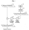
- FIG. 1 illustrates liquid crystal devices and sources of mura.
- mura defects may occur as a result of various components of the display such as LC120, Digital Analog Converter (DAC) 130 and so on.
- mura defects may occur as a result of Voltage-Domain Nonuniformities 140, Illumination Nonuniformities 150 and so on.
- the combination of the light sources (e.g., fluorescent tubes or light emitting diodes) and the diffuser results in very low frequency modulations as opposed to a uniform field in the resulting displayed image.
- the LCD panel itself may be a source of mura defects because of non-uniformity in the liquid crystal material deposited on the glass.
- This type of mura tends to be low frequency with strong asymmetry, that is, it may appear streaky which has some higher frequency components in a single direction.
- Another source of mura defects tends to be the driving circuitry (e.g., clocking noise) which causes grid like distortions on the display.
- Yet another source of mura defects is pixel noise, which is primarily due to variations in the localized driving circuitry (e.g., the thin film transistors) and is usually manifested as a fixed pattern noise.
- WO 93/19453 on which the two-part form is based, discloses a flat panel display inspection system comprising a camera for detecting, for example, the brightness uniformity across the display. According to an embodiment, errors in the detected image may be avoided by calculating compensation factors that may be applied to the display drivers. Accordingly, the brightness uniformity may be corrected.
- WO 97/00452 refers to a mura detection apparatus and method, wherein an image of the display is taken and processed.
- WO 2004/047058 refers to a method of improving the output uniformity of a display device.
- EP-A-1211661 discloses a process for producing a display having a luminance-correcting function.
- JP 2006 084729 is concerned with providing a luminance correction method and a display system, which are capable of resolving luminance unevenness neither too much nor too little.
- a measured luminance of each prescribed pixel position at the time of displaying a display image having each prescribed pixel value on a display panel is prestored in a hard disk, and a correction value is calculated in an arithmetic part on the basis of a target luminance, the measured luminance, and gradation characteristics of the display panel, and the calculated correction value is used to correct each pixel value of an image to be displayed on the display panel.
- a target luminance for one prescribed pixel value is determined by the arithmetic part, and a target luminance for another prescribed pixel value is calculated in the arithmetic part on the basis of the determined target luminance and the gradation characteristics of the display panel.
- JP 2005 221525 is concerned with providing a display device which emits light with uniform brightness by correcting luminance unevenness of the display device without the impairment of the gradation performance.
- the light emission luminance of phosphors to respective electron emitters is measured by a first measuring section and is then converted to peak values which are thereafter stored into a correction table (LUT). If there is a variation in the light emission luminance, an element characteristic correction section performs correction by discretely reforming the respective element characteristics in such a manner that the uniform element characteristics can be attained.
- the light emission luminance of the phosphors corresponding to the respective electron emitters is further measured by a second measuring section and thereafter the LUT is formed and if there is the variation in the light emission luminance, the display device is applied in the video display based on the correction LUT.
- the mura defects due to the thin film transistor noise and driver circuits does not occur in the luminance domain, but rather occurs in the voltage domain.
- the result manifests itself in the LCD response curse which is usually an S-shaped function of luminance.
- An object of the present invention is to provide a more straightforward approach which is to measure and correct the resulting tone scale for each pixel of the display, rather than correct for each non-uniformity in their different domains.
- a more straightforward approach is to measure the resulting tone scale for each pixel of the display.
- the low frequency mura non-uniformities as well as the higher frequency fixed pattern mura non-uniformity will appear as distortions in the displayed tone scale.
- additive distortions in the code value domain will show up as vertical offsets in the tone scale's of the pixels affected by such a distortion.
- Illumination based distortions which are additive in the log domain will show up as non-linear additions in the tone scale.
- the system may reflect the issues occurring in the different domains back to the code value domain. If each pixel's tonescale is forced to be identical (or substantially so), then at each gray level all of the pixels will have the same luminance (or substantially so), thus the mura will be reduced to zero (or substantially so).
- FIG. 2 illustrates capturing mura tonescale.
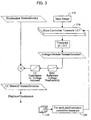
- FIG. 3 illustrates loading correction mura tonescales.
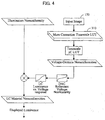
- FIG. 4 illustrates input imagery and loaded mura correction tonescale.
- the process of detecting and correcting for mura defects may be done as a set of steps.
- the capture and generation of the corrective tone scale is created which may be expressed in the form of a look up table. Initially, values in the look up table are set to a uniform value k before the display is measured (220), and converted to ⁇ by a tonescale ⁇ C look up table 160.
- mura is captured by a camera (210).
- the tonescale is stored for each pixel (230), and a corrective tonescale is calculated for each pixel (240).
- the corrective tone scale may be applied to a mura look up table which operates on the frame buffer memory of the display.
- the display is used to receive image data which is modified by the mura look up table (310), prior to being displayed on the display.
- the first step is to use an image capture device, such as a camera, to capture the mura as a function of gray level.
- the camera should have a resolution equal to or greater than the display so that there is at least one pixel in the camera image corresponding to each display pixel. For high resolution displays or low resolution cameras, the camera may be shifted in steps across the display to characterize the entire display.
- the captured images are combined so that a tone scale across its display range is generated for each pixel (or a sub-set thereof). If the display has zero mura, then the corrective mura tone scales would all be the same.
- a corrective tone scale for each pixel is determined so that the combination of the corrective tone scale together with the system non-uniformity provides a resulting tone scale that is substantially uniform across the display. Initially, the values in the mura correction tone scale look up table may be set to unity before the display is measured. After determining the corrective mura tone scale values for each pixel, it is loaded into the display memory as shown in FIG. 4 .
- any flat field will appear uniform, and even mura that may be visible on ramped backgrounds, such as a sky gradient, will be set to zero.
- the mura reduction technique is effective for reducing display non-uniformities, it also tends to reduce the dynamic range, namely, the maximum to minimum in luminance levels. Moreover, the reduction in the dynamic range also depends on the level of mura which varies from display to display, thus making the resulting dynamic range of the display variable. For example, the mura on the left side of the display may be less bright than the mura on the right side of the display. This is typical for mura due to illumination non-uniformity, and this will tend to be the case for all gray levels. Since the mura correction can not make a pixel brighter than its max, the effect of mura correction is to lower the luminance of the left side to match the maximum value of the darker side.
- the darker right side can at best match the black level of the lighter left side.
- the corrected maximum gets reduced to the lowest maximum value across the display, and the corrected minimum gets elevated to the lightest minimum value across the display.
- the dynamic range e.g., log max - log min
- the same reduction in dynamic range also occurs for the other non-uniformities.
- a high amplitude fixed pattern noise leads to a reduction of overall dynamic range after mura correction.
- the technique of capturing the mura from the pixels and thereafter correcting the mura using a look up table may be relatively accurate within the signal to noise ratio of the image capture apparatus and the bit-depth of the mural correction look up table. However, it was determined that taking into account that actual effects of the human visual system that will actually view the display may result in a greater dynamic range than would otherwise result.
- some mura effects of particular frequencies are corrected in such a manner that the changes may not be visible to the viewer.
- the dynamic range of the display is reduced while the viewer will not otherwise perceive a difference in the displayed image.
- a slight gradient across the image so that the left side is darker than the right side may be considered a mura effect.
- the human visual system has very low sensitivity to such a low frequency mura artifact and thus may not be sufficiently advantageous to remove. That is, it generally takes a high amplitude of such mura waveforms to be readily perceived by the viewer. If the mura distortion is generally imperceptible to the viewer, although physically measurable, then it is not useful to modify it.
- FIG. 5 illustrates contrast sensitivity function dependence on viewing angle.
- one measure of the human visual system is a contrast sensitivity function (CSF) of the human eye. This is one of several criteria that may be used so that only the mura that is readily visible to the eye is corrected. This has the benefit of maintaining a higher dynamic range of the correction than the technique illustrated in FIGS. 3-5 .
- CSF contrast sensitivity function
- the CSF of the human visual system is a function of spatial frequencies and thus should be mapped to digital frequencies for use in mura reduction. Such a mapping is dependent on the viewing distance.
- the CSF changes shape, maximum sensitivity, and bandwidth is a function of the viewing conditions, such as light adaptation level, display size, etc. As a result the CSF should be chosen for the conditions that match that of the display and its anticipated viewing conditions.
- the CSF may be converted to a point spread function (psf) and then used to filter the captured mura images via convolution. Typically, there is a different point spread function for each gray level.
- the filtering may be done by leaving the CSF in the frequency domain and converting the mura images to the frequency domain for multiplication with the CSF, and then convert back to the spatial domain via inverse Fourier transform.
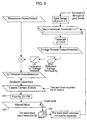
- FIG. 6 illustrates a contrast sensitivity model to attenuate the mura correction to maintain a higher dynamic range.
- a system that includes mura capture, corrective mura tone scale calculation, CSF filtered, and mura correction tone scale look up table is illustrated.
- CSF 610
- FIG. 7 illustrates the effects of using the CSF to maintain bandwidth.
- the corrective data may be based upon a weighting function that emphasizes a mid-range over a low range and a high range.
- the dynamic range of the image displayed on the display may be greater than it would have otherwise been had the characteristics generally not visible by the human visual system been considered.
Landscapes
- Engineering & Computer Science (AREA)
- Physics & Mathematics (AREA)
- Computer Hardware Design (AREA)
- General Physics & Mathematics (AREA)
- Theoretical Computer Science (AREA)
- Control Of Indicators Other Than Cathode Ray Tubes (AREA)
- Liquid Crystal Display Device Control (AREA)
- Image Processing (AREA)
- Liquid Crystal (AREA)
- Testing Of Optical Devices Or Fibers (AREA)
Description
- The present invention relates to a system for detecting defects in a displayed image. More specifically, the present invention relates to a system for detecting and correcting mura defects in a displayed image.
- The number of liquid crystal displays, electroluminescent displays, organic light emitting devices, plasma displays, and other types of displays are increasing. The increasing demand for such displays has resulted in significant investments to create high quality production facilities to manufacture high quality displays.
- Despite the significant investment, the display industry still primarily relies on the use of human operators to perform the final test and inspection of displays. The operator performs visual inspections of each display for defects, and accepts or rejects the display based upon the operator's perceptions. Such inspection includes, for example, pixel-based defects and area-based defects. The quality of the resulting inspection is dependent on the individual operator is inspection which are subjective and prone to error.
- "Mura" defects are contrast-type defects, where one or more pixels is brighter or darker than surrounding pixels, when they should have uniform luminance. For example, when an intended flat region of color is displayed, various imperfections in the display components may result in undesirable modulations of the luminance. Mura defects may also be referred to as "Alluk" defects or generally non-uniformity distortions. Generically, such contrast-type defects may be identified as "blobs", "bands", "streaks", etc. There are many stages in the manufacturing process that may result in Mura defects on the display.
- Mura defects may appear as low frequency, high-frequency, noise-like, and/or very structured patterns on the display. In general, most Mura defects tend to be static in time once a display is constructed. However, some Mura defects that are time dependent include pixel defects as well as various types of non-uniform aging, yellowing, and burn in. Display non-uniformity deviations that are due to the input signal (such as image capture noise) are not considered Mura defects.
-
FIG. 1 illustrates liquid crystal devices and sources of mura. Referring toFIG. 1 , mura defects may occur as a result of various components of the display such as LC120, Digital Analog Converter (DAC) 130 and so on. Moreover, mura defects may occur as a result of Voltage-Domain Nonuniformities 140,Illumination Nonuniformities 150 and so on. The combination of the light sources (e.g., fluorescent tubes or light emitting diodes) and the diffuser results in very low frequency modulations as opposed to a uniform field in the resulting displayed image. The LCD panel itself may be a source of mura defects because of non-uniformity in the liquid crystal material deposited on the glass. This type of mura tends to be low frequency with strong asymmetry, that is, it may appear streaky which has some higher frequency components in a single direction. Another source of mura defects tends to be the driving circuitry (e.g., clocking noise) which causes grid like distortions on the display. Yet another source of mura defects is pixel noise, which is primarily due to variations in the localized driving circuitry (e.g., the thin film transistors) and is usually manifested as a fixed pattern noise. -
WO 93/19453 WO 97/00452 WO 2004/047058 refers to a method of improving the output uniformity of a display device. In addition,EP-A-1211661 discloses a process for producing a display having a luminance-correcting function. -
JP 2006 084729 -
JP 2005 221525 - What is needed is improved Mura reduction techniques.
- The above objects are achieved by the claimed matter according to the independent claims.
- Additional objects, features, and strengths of the present invention will be made clear by the description below. Further, the advantages of the present invention will be evident from the following explanation in reference to the drawings.
-
-
FIG. 1 illustrates liquid crystal devices and sources of mura. -
FIG. 2 illustrates capturing mura tonescale. -
FIG. 3 illustrates loading correction mura tonescales. -
FIG. 4 illustrates input imagery and loaded mura correction tonescale. -
FIG. 5 illustrates contrast sensitivity function dependence on viewing angle. -
FIG. 6 illustrates a contrast sensitivity model to attenuate the mura correction to maintain a higher dynamic range. -
FIG. 7 illustrates examples of mura correction with and without using the contrast sensitivity model. - The present invention is not limited to the description of the embodiments above, but may be altered by a skilled person within the scope of the claims. An embodiment based on a proper combination of technical means disclosed in different embodiments is encompassed in the technical scope of the present invention.
- The embodiments and concrete examples of implementation discussed in the foregoing detailed explanation serve solely to illustrate the technical details of the present invention, which should not be narrowly interpreted within the limits of such embodiments and concrete examples, but rather may be applied in many variations, provided such variations do not exceed the scope of the patent claims set forth below.
- The continual quality improvement in display components reduces mura defects but unfortunately mura defects still persist even on the best displays. Referring to
FIG. 1 , identification of mura defects is not straightforward because the source of the mura arise in different luminance domains. The mura resulting from the illumination source occurs in the linear luminance domain. To compensate for this effect from the linear domain, the LCD luminance image is divided by the mura and then re-normalized to the desired maximum level. This effect in the linear domain may also be compensated by addition in the log domain. Unfortunately, the data displayed on the image domain of the image in the LCD code value space is neither linear nor log luminance. Accordingly, the LCD image data should be converted to either of these domains for correction. - The mura defects due to the thin film transistor noise and driver circuits does not occur in the luminance domain, but rather occurs in the voltage domain. The result manifests itself in the LCD response curse which is usually an S-shaped function of luminance.
- Variations in the mura effect due to variations in liquid crystal material occur in yet another domain, depending on if it is due to thickness of the liquid crystal material, or due to its active attenuation properties changing across the display. The present invention is accomplished in view of the problems discussed above. An object of the present invention is to provide a more straightforward approach which is to measure and correct the resulting tone scale for each pixel of the display, rather than correct for each non-uniformity in their different domains.
- Rather than correct for each non-uniformity in their different domains, a more straightforward approach is to measure the resulting tone scale for each pixel of the display. The low frequency mura non-uniformities as well as the higher frequency fixed pattern mura non-uniformity will appear as distortions in the displayed tone scale. For example, additive distortions in the code value domain will show up as vertical offsets in the tone scale's of the pixels affected by such a distortion. Illumination based distortions which are additive in the log domain will show up as non-linear additions in the tone scale. By measuring the tone scale per pixel, where the tone scale is a mapping from code value to luminance, the system may reflect the issues occurring in the different domains back to the code value domain. If each pixel's tonescale is forced to be identical (or substantially so), then at each gray level all of the pixels will have the same luminance (or substantially so), thus the mura will be reduced to zero (or substantially so).
-
FIG. 2 illustrates capturing mura tonescale.FIG. 3 illustrates loading correction mura tonescales.FIG. 4 illustrates input imagery and loaded mura correction tonescale. Referring toFIG. 2 , the process of detecting and correcting for mura defects may be done as a set of steps. First, the capture and generation of the corrective tone scale is created which may be expressed in the form of a look up table. Initially, values in the look up table are set to a uniform value k before the display is measured (220), and converted to γ by a tonescale γ C look up table 160. After the same process as illustrated inFIG.1 , mura is captured by a camera (210). Then, the tonescale is stored for each pixel (230), and a corrective tonescale is calculated for each pixel (240). Second, referring toFIG. 3 the corrective tone scale may be applied to a mura look up table which operates on the frame buffer memory of the display. Third, referring toFIG. 4 , the display is used to receive image data which is modified by the mura look up table (310), prior to being displayed on the display. - The first step is to use an image capture device, such as a camera, to capture the mura as a function of gray level. The camera should have a resolution equal to or greater than the display so that there is at least one pixel in the camera image corresponding to each display pixel. For high resolution displays or low resolution cameras, the camera may be shifted in steps across the display to characterize the entire display. The preferable test patterns provided to and displayed on the display include uniform fields (all code values = k) and captured by the camera. The test pattern and capture are done for all of the code values of the displays tone scale (e.g., 256 code values for 8 bit / color display). Alternatively, a subset of the tone scales may be used, in which case typically the non-sampled tone values are interpolated.
- The captured images are combined so that a tone scale across its display range is generated for each pixel (or a sub-set thereof). If the display has zero mura, then the corrective mura tone scales would all be the same. A corrective tone scale for each pixel is determined so that the combination of the corrective tone scale together with the system non-uniformity provides a resulting tone scale that is substantially uniform across the display. Initially, the values in the mura correction tone scale look up table may be set to unity before the display is measured. After determining the corrective mura tone scale values for each pixel, it is loaded into the display memory as shown in
FIG. 4 . - Referring to
FIG. 5 , with the mura corrective tone scale data loaded any flat field will appear uniform, and even mura that may be visible on ramped backgrounds, such as a sky gradient, will be set to zero. - While this mura reduction technique is effective for reducing display non-uniformities, it also tends to reduce the dynamic range, namely, the maximum to minimum in luminance levels. Moreover, the reduction in the dynamic range also depends on the level of mura which varies from display to display, thus making the resulting dynamic range of the display variable. For example, the mura on the left side of the display may be less bright than the mura on the right side of the display. This is typical for mura due to illumination non-uniformity, and this will tend to be the case for all gray levels. Since the mura correction can not make a pixel brighter than its max, the effect of mura correction is to lower the luminance of the left side to match the maximum value of the darker side. In addition, for the black level, the darker right side can at best match the black level of the lighter left side. As a result, the corrected maximum gets reduced to the lowest maximum value across the display, and the corrected minimum gets elevated to the lightest minimum value across the display. Thus, the dynamic range (e.g., log max - log min) of the corrected display will be less than either the range of the left or right sides, and consequently it is lower than the uncorrected display. The same reduction in dynamic range also occurs for the other non-uniformities. As an example, a high amplitude fixed pattern noise leads to a reduction of overall dynamic range after mura correction.
- The technique of capturing the mura from the pixels and thereafter correcting the mura using a look up table may be relatively accurate within the signal to noise ratio of the image capture apparatus and the bit-depth of the mural correction look up table. However, it was determined that taking into account that actual effects of the human visual system that will actually view the display may result in a greater dynamic range than would otherwise result.
- By way of example, some mura effects of particular frequencies are corrected in such a manner that the changes may not be visible to the viewer. Thus the dynamic range of the display is reduced while the viewer will not otherwise perceive a difference in the displayed image. By way of example, a slight gradient across the image so that the left side is darker than the right side may be considered a mura effect. The human visual system has very low sensitivity to such a low frequency mura artifact and thus may not be sufficiently advantageous to remove. That is, it generally takes a high amplitude of such mura waveforms to be readily perceived by the viewer. If the mura distortion is generally imperceptible to the viewer, although physically measurable, then it is not useful to modify it.
-
FIG. 5 illustrates contrast sensitivity function dependence on viewing angle. Referring toFIG. 5 , one measure of the human visual system is a contrast sensitivity function (CSF) of the human eye. This is one of several criteria that may be used so that only the mura that is readily visible to the eye is corrected. This has the benefit of maintaining a higher dynamic range of the correction than the technique illustrated inFIGS. 3-5 . - The CSF of the human visual system is a function of spatial frequencies and thus should be mapped to digital frequencies for use in mura reduction. Such a mapping is dependent on the viewing distance. The CSF changes shape, maximum sensitivity, and bandwidth is a function of the viewing conditions, such as light adaptation level, display size, etc. As a result the CSF should be chosen for the conditions that match that of the display and its anticipated viewing conditions.
- The CSF may be converted to a point spread function (psf) and then used to filter the captured mura images via convolution. Typically, there is a different point spread function for each gray level. The filtering may be done by leaving the CSF in the frequency domain and converting the mura images to the frequency domain for multiplication with the CSF, and then convert back to the spatial domain via inverse Fourier transform.
-
FIG. 6 illustrates a contrast sensitivity model to attenuate the mura correction to maintain a higher dynamic range. Referring toFIG. 6 , a system that includes mura capture, corrective mura tone scale calculation, CSF filtered, and mura correction tone scale look up table is illustrated. As illustrated inFIG. 6 , after mura is captured by the camera, filtering is performed by CSF (610). This maintains a higher dynamic range of the correction.FIG. 7 illustrates the effects of using the CSF to maintain bandwidth. - In the display, the corrective data may be based upon a weighting function that emphasizes a mid-range over a low range and a high range.
- In the display, the dynamic range of the image displayed on the display may be greater than it would have otherwise been had the characteristics generally not visible by the human visual system been considered.
- The terms and expressions which have been employed in the foregoing specification are used therein as terms of description and not of limitation, and there is no intention, in the use of such terms and expressions, of excluding equivalents of the features shown and described or portions thereof, it being recognized that the scope of the invention is defined and limited only by the claims which follow.
Claims (12)
- A method for reducing non-uniformity defects in a display having a tone scale driven by respective input luminance code values to said display, the method comprising:- causing illumination at a plurality of pixels at each of a plurality of gray levels, each one of said plurality of gray levels corresponding to a respective input luminance code value to said display;- capturing said display with an image sensing device external to said display et each one of the illuminated gray levels;- combining the captured images to generate a tone scale for each pixel- determining corrective data (240) for said pixels so as to reduce the non-uniformity defects of said display;- storing said corrective data (310) in said display to process an image received by said display so as to reduce said non-uniformity defects;characterized in that
said corrective data (310) are determined for said pixels by using a contrast sensitivity function (CSF) of the human eye so as to reduce the non-uniformity defects of said display for those characteristics visible by the human visual system and so as not to reduce the non-uniformity defects of the display for those characteristics not visible by the human visual system. - The method of claim 1 wherein said plurality of pixels include substantially all of the pixels of said display.
- The method of claim 1 wherein said plurality of gray levels include substantially all of the gray levels of said display.
- The method of claim 1 wherein said capturing is with a camera having a resolution greater than that of the display.
- The method of claim 4 wherein at least one sensing element for each of said pixels of said display.
- The method of claim 1 wherein said gray levels include less than all of the tone scale of said display.
- The method of claim 6 wherein fewer tone scales of the lower range of said tone scale is used than the higher scales of said tone scale.
- The method of claim 1 wherein corrective data are provided for each pixel of said display.
- The method of claim 1, wherein determining corrective data (240) for said pixels comprises determining a corrective tone scale for each pixel.
- The method of claim 1, wherein said determining is based upon a weighting function that emphasizes a mid-range over a low range and a high range that results in a greater dynamic range of said image.
- The method of claim 1, wherein as a result of using said corrective data the dynamic range of said image displayed on said display is greater than it would have otherwise been had the characteristics generally not visible by the human visual system been considered.
- A display having a tone scale driven by respective luminance code values to said display, the display comprising:a plurality of pixels each of said pixels being adapted to cause illumination with at least one of a plurality of gray levels, each one of said plurality of gray levels corresponding to a respective input luminance code valuecharacterized in thatsaid display is adapted to apply a corrective tone scale based on corrective data (310) for each pixel so as to reduce the non-uniformity defects of said display;wherein the corrective data (310) are determined by applying the method of any one of claims 1 to 12 to the display.
Applications Claiming Priority (1)
| Application Number | Priority Date | Filing Date | Title |
|---|---|---|---|
| US11/731,094 US8026927B2 (en) | 2007-03-29 | 2007-03-29 | Reduction of mura effects |
Publications (3)
| Publication Number | Publication Date |
|---|---|
| EP1975915A2 EP1975915A2 (en) | 2008-10-01 |
| EP1975915A3 EP1975915A3 (en) | 2009-05-27 |
| EP1975915B1 true EP1975915B1 (en) | 2016-11-02 |
Family
ID=39542049
Family Applications (1)
| Application Number | Title | Priority Date | Filing Date |
|---|---|---|---|
| EP08005830.8A Not-in-force EP1975915B1 (en) | 2007-03-29 | 2008-03-27 | Reduction of mura effects, and display |
Country Status (3)
| Country | Link |
|---|---|
| US (1) | US8026927B2 (en) |
| EP (1) | EP1975915B1 (en) |
| JP (2) | JP2008250319A (en) |
Families Citing this family (31)
| Publication number | Priority date | Publication date | Assignee | Title |
|---|---|---|---|---|
| TWI375198B (en) * | 2007-05-17 | 2012-10-21 | Tpo Displays Corp | A system for displaying images |
| US8049695B2 (en) * | 2007-10-15 | 2011-11-01 | Sharp Laboratories Of America, Inc. | Correction of visible mura distortions in displays by use of flexible system for memory resources and mura characteristics |
| JP5362753B2 (en) * | 2008-07-31 | 2013-12-11 | 株式会社イクス | Image quality adjustment apparatus and image correction data generation program |
| US20110012908A1 (en) * | 2009-07-20 | 2011-01-20 | Sharp Laboratories Of America, Inc. | System for compensation of differential aging mura of displays |
| GB2473614A (en) * | 2009-09-16 | 2011-03-23 | Sharp Kk | Private display with main and side images and axis-dependent luminance control |
| KR101699089B1 (en) | 2010-04-05 | 2017-01-23 | 가부시키가이샤 제이올레드 | Display method of organic EL display device and organic EL display device |
| WO2011125113A1 (en) | 2010-04-05 | 2011-10-13 | パナソニック株式会社 | Organic el display device and method for manufacturing an organic el display device |
| WO2012005284A1 (en) * | 2010-07-07 | 2012-01-12 | シャープ株式会社 | Liquid-crystal display device |
| US20120075354A1 (en) * | 2010-09-29 | 2012-03-29 | Sharp Laboratories Of America, Inc. | Capture time reduction for correction of display non-uniformities |
| JPWO2014128822A1 (en) * | 2013-02-19 | 2017-02-02 | 株式会社イクス | Correction data generation method, correction data generation system, and image quality adjustment technique using them |
| CN103761933A (en) * | 2013-12-30 | 2014-04-30 | 深圳市华星光电技术有限公司 | System and method for repairing bad display area of liquid crystal display panel |
| JP6341672B2 (en) * | 2014-01-23 | 2018-06-13 | キヤノン株式会社 | Image processing apparatus, image processing method, and program |
| CN103854556B (en) | 2014-02-19 | 2016-05-18 | 北京京东方显示技术有限公司 | The voltage compensating device of primary color sub-pixels and method, display unit |
| TWI625714B (en) * | 2014-02-21 | 2018-06-01 | 群創光電股份有限公司 | Oled display |
| CN104217701A (en) * | 2014-08-22 | 2014-12-17 | 京东方科技集团股份有限公司 | Display panel control method, display panel control device and time schedule controller |
| US10341637B1 (en) * | 2015-03-11 | 2019-07-02 | Facebook Technologies, Llc | Full frame uniformity across panels |
| WO2016149877A1 (en) * | 2015-03-20 | 2016-09-29 | 华为技术有限公司 | Method for correcting screen asymmetry and device and system thereof |
| JP6577223B2 (en) * | 2015-04-21 | 2019-09-18 | シャープ株式会社 | Liquid crystal display |
| CN105244001B (en) * | 2015-11-09 | 2018-01-09 | 深圳市华星光电技术有限公司 | A kind of method and device of determination mura offsets |
| CN109073503B (en) * | 2016-04-28 | 2020-10-09 | 株式会社宜科思 | Non-uniformity evaluation method and non-uniformity evaluation device |
| US10916211B2 (en) | 2016-09-27 | 2021-02-09 | Sakai Display Products Corporation | Method for correcting luminance non-uniformity in liquid crystal display apparatus, and correction data generation device |
| CN106898286B (en) * | 2017-03-15 | 2020-07-03 | 武汉精测电子集团股份有限公司 | Mura defect repairing method and device based on designated position |
| WO2019024094A1 (en) * | 2017-08-04 | 2019-02-07 | 深圳市柔宇科技有限公司 | Mura detection method and mura detection system |
| US10755133B2 (en) * | 2018-02-22 | 2020-08-25 | Samsung Display Co., Ltd. | System and method for line Mura detection with preprocessing |
| CN109147696B (en) | 2018-09-03 | 2021-02-26 | 重庆惠科金渝光电科技有限公司 | Data processing method, display device, and computer-readable storage medium |
| CN109036277B (en) * | 2018-09-27 | 2020-06-09 | 京东方科技集团股份有限公司 | Compensation method and compensation device, display method and storage medium |
| CN109358438B (en) * | 2018-10-30 | 2021-03-26 | 京东方科技集团股份有限公司 | Moiré evaluation method, device and system |
| JP2021081494A (en) * | 2019-11-15 | 2021-05-27 | シャープ株式会社 | Image processing system, image processing method, and image processing program |
| CN111583863B (en) * | 2020-05-25 | 2021-08-27 | 昆山国显光电有限公司 | Mura compensation method and device and display panel |
| KR20240022084A (en) * | 2022-08-11 | 2024-02-20 | 주식회사 엘엑스세미콘 | Apparatus and Method for Compensating Mura |
| CN119993066B (en) * | 2025-04-01 | 2025-09-23 | 京东方科技集团股份有限公司 | Display panel brightness compensation method, medium and device |
Citations (2)
| Publication number | Priority date | Publication date | Assignee | Title |
|---|---|---|---|---|
| JP2005221525A (en) * | 2004-02-03 | 2005-08-18 | Canon Inc | Display device |
| JP2006084729A (en) * | 2004-09-15 | 2006-03-30 | Nanao Corp | Luminance correction method and display system |
Family Cites Families (19)
| Publication number | Priority date | Publication date | Assignee | Title |
|---|---|---|---|---|
| JPH07507139A (en) | 1992-03-16 | 1995-08-03 | フォトン・ダイナミクス・インコーポレーテッド | flat panel display inspection system |
| US5917935A (en) * | 1995-06-13 | 1999-06-29 | Photon Dynamics, Inc. | Mura detection apparatus and method |
| US6154561A (en) * | 1997-04-07 | 2000-11-28 | Photon Dynamics, Inc. | Method and apparatus for detecting Mura defects |
| JP2001324961A (en) | 2000-03-10 | 2001-11-22 | Ngk Insulators Ltd | Display device manufacturing method |
| US7110012B2 (en) * | 2000-06-12 | 2006-09-19 | Sharp Laboratories Of America, Inc. | System for improving display resolution |
| JP3431075B2 (en) * | 2001-08-27 | 2003-07-28 | 科学技術振興事業団 | Liquid crystal display panel unevenness classification processing method, apparatus and program |
| KR100422295B1 (en) * | 2002-05-18 | 2004-03-11 | 엘지.필립스 엘시디 주식회사 | Image quality analysis method and system for display device |
| CN100472595C (en) | 2002-11-21 | 2009-03-25 | 皇家飞利浦电子股份有限公司 | Method for improving output uniformity of a display device |
| JP2004212311A (en) * | 2003-01-08 | 2004-07-29 | Seiko Epson Corp | Mura defect detection method and apparatus |
| US20040179028A1 (en) * | 2003-03-12 | 2004-09-16 | Fuji Photo Film Co., Ltd. | Pixel defect correcting method, color mura correcting method and image display device |
| JP4036142B2 (en) * | 2003-05-28 | 2008-01-23 | セイコーエプソン株式会社 | Electro-optical device, driving method of electro-optical device, and electronic apparatus |
| JP2005017715A (en) | 2003-06-26 | 2005-01-20 | Toshiba Corp | Surface unevenness correction apparatus and surface unevenness correction method |
| US6937249B2 (en) * | 2003-11-07 | 2005-08-30 | Integrated Color Solutions, Inc. | System and method for display device characterization, calibration, and verification |
| JP2005316408A (en) * | 2004-03-30 | 2005-11-10 | Sanyo Electric Co Ltd | Display unevenness correction value generation device |
| US20060034536A1 (en) * | 2004-06-23 | 2006-02-16 | Ogren Wayne E | Systems and methods relating to magnitude enhancement analysis suitable for high bit level displays on low bit level systems, determining the material thickness, and 3D visualization of color space dimensions |
| JP2006018169A (en) * | 2004-07-05 | 2006-01-19 | Sony Corp | Image display device and temperature correction method thereof |
| DE602004024895D1 (en) | 2004-10-25 | 2010-02-11 | Barco Nv | Optical correction for light panels with high uniformity |
| JP4857586B2 (en) * | 2005-04-05 | 2012-01-18 | セイコーエプソン株式会社 | Electronic circuit driving method and driving circuit, light emitting device, and electronic apparatus |
| KR101137856B1 (en) * | 2005-10-25 | 2012-04-20 | 엘지디스플레이 주식회사 | Flat Display Apparatus And Picture Quality Controling Method Thereof |
-
2007
- 2007-03-29 US US11/731,094 patent/US8026927B2/en not_active Expired - Fee Related
-
2008
- 2008-03-19 JP JP2008072423A patent/JP2008250319A/en active Pending
- 2008-03-27 EP EP08005830.8A patent/EP1975915B1/en not_active Not-in-force
-
2009
- 2009-01-14 JP JP2009005586A patent/JP2009122690A/en active Pending
Patent Citations (2)
| Publication number | Priority date | Publication date | Assignee | Title |
|---|---|---|---|---|
| JP2005221525A (en) * | 2004-02-03 | 2005-08-18 | Canon Inc | Display device |
| JP2006084729A (en) * | 2004-09-15 | 2006-03-30 | Nanao Corp | Luminance correction method and display system |
Also Published As
| Publication number | Publication date |
|---|---|
| US20080238934A1 (en) | 2008-10-02 |
| JP2008250319A (en) | 2008-10-16 |
| JP2009122690A (en) | 2009-06-04 |
| EP1975915A2 (en) | 2008-10-01 |
| US8026927B2 (en) | 2011-09-27 |
| EP1975915A3 (en) | 2009-05-27 |
Similar Documents
| Publication | Publication Date | Title |
|---|---|---|
| US8026927B2 (en) | Reduction of mura effects | |
| US8049695B2 (en) | Correction of visible mura distortions in displays by use of flexible system for memory resources and mura characteristics | |
| US20110012908A1 (en) | System for compensation of differential aging mura of displays | |
| US8610654B2 (en) | Correction of visible mura distortions in displays using filtered mura reduction and backlight control | |
| US20120075354A1 (en) | Capture time reduction for correction of display non-uniformities | |
| US20100013750A1 (en) | Correction of visible mura distortions in displays using filtered mura reduction and backlight control | |
| CN107818766B (en) | Integrated circuit for driving display panel and method thereof | |
| CN101685612B (en) | Backlight luminance control apparatus and video display apparatus | |
| KR101333680B1 (en) | Display apparatus and method of adjusting brightness for the same | |
| CN111883038A (en) | Method for determining gray-scale value of pixel, display panel and computer-readable storage medium | |
| US9990878B2 (en) | Data clipping method using red, green, blue and white data, and display device using the same | |
| JP2019514041A (en) | Compensation method of unevenness phenomenon | |
| TWI525604B (en) | Apparatus and method for image analysis and image display | |
| US12112676B2 (en) | Demura method for display panel | |
| JP5174837B2 (en) | Display device, luminance unevenness correction method, correction data creation device, and correction data creation method | |
| JP2009128733A (en) | Liquid crystal display device, control circuit, liquid crystal display control method, and computer program | |
| KR101389359B1 (en) | Display apparatus and method of adjusting brightness for the same | |
| CN118781985B (en) | Grayscale debugging method for display panel and display panel | |
| Klompenhouwer | The temporal MTF of displays and related video signal processing | |
| WO2019192139A1 (en) | Image processing method for display device | |
| US7817876B2 (en) | Method of noisy signal analysis and apparatus thereof | |
| KR20050084308A (en) | Color non-uniformity correction method and apparatus having optical and electronic lcd panel compensation | |
| CN107886918B (en) | Real-time video image correction method | |
| CN117524046A (en) | Display device and over-driving method thereof | |
| CN120932601A (en) | Method for improving display brightness consistency of complete television |
Legal Events
| Date | Code | Title | Description |
|---|---|---|---|
| PUAI | Public reference made under article 153(3) epc to a published international application that has entered the european phase |
Free format text: ORIGINAL CODE: 0009012 |
|
| AK | Designated contracting states |
Kind code of ref document: A2 Designated state(s): AT BE BG CH CY CZ DE DK EE ES FI FR GB GR HR HU IE IS IT LI LT LU LV MC MT NL NO PL PT RO SE SI SK TR |
|
| AX | Request for extension of the european patent |
Extension state: AL BA MK RS |
|
| RIN1 | Information on inventor provided before grant (corrected) |
Inventor name: OZAWA, YASUO Inventor name: DALY, SCOTT J. |
|
| PUAL | Search report despatched |
Free format text: ORIGINAL CODE: 0009013 |
|
| AK | Designated contracting states |
Kind code of ref document: A3 Designated state(s): AT BE BG CH CY CZ DE DK EE ES FI FR GB GR HR HU IE IS IT LI LT LU LV MC MT NL NO PL PT RO SE SI SK TR |
|
| AX | Request for extension of the european patent |
Extension state: AL BA MK RS |
|
| 17P | Request for examination filed |
Effective date: 20091117 |
|
| 17Q | First examination report despatched |
Effective date: 20100104 |
|
| AKX | Designation fees paid |
Designated state(s): DE FR GB |
|
| GRAP | Despatch of communication of intention to grant a patent |
Free format text: ORIGINAL CODE: EPIDOSNIGR1 |
|
| INTG | Intention to grant announced |
Effective date: 20160602 |
|
| GRAS | Grant fee paid |
Free format text: ORIGINAL CODE: EPIDOSNIGR3 |
|
| GRAA | (expected) grant |
Free format text: ORIGINAL CODE: 0009210 |
|
| AK | Designated contracting states |
Kind code of ref document: B1 Designated state(s): DE FR GB |
|
| REG | Reference to a national code |
Ref country code: GB Ref legal event code: FG4D |
|
| REG | Reference to a national code |
Ref country code: DE Ref legal event code: R096 Ref document number: 602008047126 Country of ref document: DE |
|
| REG | Reference to a national code |
Ref country code: DE Ref legal event code: R097 Ref document number: 602008047126 Country of ref document: DE |
|
| PLBE | No opposition filed within time limit |
Free format text: ORIGINAL CODE: 0009261 |
|
| STAA | Information on the status of an ep patent application or granted ep patent |
Free format text: STATUS: NO OPPOSITION FILED WITHIN TIME LIMIT |
|
| 26N | No opposition filed |
Effective date: 20170803 |
|
| GBPC | Gb: european patent ceased through non-payment of renewal fee |
Effective date: 20170327 |
|
| REG | Reference to a national code |
Ref country code: FR Ref legal event code: ST Effective date: 20171130 |
|
| PG25 | Lapsed in a contracting state [announced via postgrant information from national office to epo] |
Ref country code: FR Free format text: LAPSE BECAUSE OF NON-PAYMENT OF DUE FEES Effective date: 20170331 |
|
| PG25 | Lapsed in a contracting state [announced via postgrant information from national office to epo] |
Ref country code: GB Free format text: LAPSE BECAUSE OF NON-PAYMENT OF DUE FEES Effective date: 20170327 |
|
| PGFP | Annual fee paid to national office [announced via postgrant information from national office to epo] |
Ref country code: DE Payment date: 20190321 Year of fee payment: 12 |
|
| REG | Reference to a national code |
Ref country code: DE Ref legal event code: R119 Ref document number: 602008047126 Country of ref document: DE |
|
| PG25 | Lapsed in a contracting state [announced via postgrant information from national office to epo] |
Ref country code: DE Free format text: LAPSE BECAUSE OF NON-PAYMENT OF DUE FEES Effective date: 20201001 |