EP1973163A2 - High temperature performance capable gallium nitride transistor - Google Patents
High temperature performance capable gallium nitride transistor Download PDFInfo
- Publication number
- EP1973163A2 EP1973163A2 EP08250197A EP08250197A EP1973163A2 EP 1973163 A2 EP1973163 A2 EP 1973163A2 EP 08250197 A EP08250197 A EP 08250197A EP 08250197 A EP08250197 A EP 08250197A EP 1973163 A2 EP1973163 A2 EP 1973163A2
- Authority
- EP
- European Patent Office
- Prior art keywords
- transistor device
- layer
- active region
- nicr
- gate
- Prior art date
- Legal status (The legal status is an assumption and is not a legal conclusion. Google has not performed a legal analysis and makes no representation as to the accuracy of the status listed.)
- Granted
Links
- JMASRVWKEDWRBT-UHFFFAOYSA-N Gallium nitride Chemical compound [Ga]#N JMASRVWKEDWRBT-UHFFFAOYSA-N 0.000 title claims description 4
- 229910002601 GaN Inorganic materials 0.000 title description 24
- 239000000463 material Substances 0.000 claims abstract description 43
- 230000004888 barrier function Effects 0.000 claims abstract description 42
- 239000004065 semiconductor Substances 0.000 claims abstract description 22
- 230000015556 catabolic process Effects 0.000 claims abstract description 11
- 238000006731 degradation reaction Methods 0.000 claims abstract description 10
- 239000010410 layer Substances 0.000 claims description 147
- 125000006850 spacer group Chemical group 0.000 claims description 46
- 229910000623 nickel–chromium alloy Inorganic materials 0.000 claims description 28
- VNNRSPGTAMTISX-UHFFFAOYSA-N chromium nickel Chemical compound [Cr].[Ni] VNNRSPGTAMTISX-UHFFFAOYSA-N 0.000 claims description 23
- 239000000788 chromium alloy Substances 0.000 claims description 19
- PXHVJJICTQNCMI-UHFFFAOYSA-N Nickel Chemical compound [Ni] PXHVJJICTQNCMI-UHFFFAOYSA-N 0.000 claims description 15
- 238000009792 diffusion process Methods 0.000 claims description 14
- 239000011651 chromium Substances 0.000 claims description 12
- 229910052804 chromium Inorganic materials 0.000 claims description 9
- 229910052581 Si3N4 Inorganic materials 0.000 claims description 8
- BASFCYQUMIYNBI-UHFFFAOYSA-N platinum Chemical compound [Pt] BASFCYQUMIYNBI-UHFFFAOYSA-N 0.000 claims description 8
- HQVNEWCFYHHQES-UHFFFAOYSA-N silicon nitride Chemical compound N12[Si]34N5[Si]62N3[Si]51N64 HQVNEWCFYHHQES-UHFFFAOYSA-N 0.000 claims description 8
- 239000011241 protective layer Substances 0.000 claims description 7
- VYZAMTAEIAYCRO-UHFFFAOYSA-N Chromium Chemical compound [Cr] VYZAMTAEIAYCRO-UHFFFAOYSA-N 0.000 claims description 6
- 229910052759 nickel Inorganic materials 0.000 claims description 6
- 229910052750 molybdenum Inorganic materials 0.000 claims description 4
- 229910052721 tungsten Inorganic materials 0.000 claims description 4
- NWAIGJYBQQYSPW-UHFFFAOYSA-N azanylidyneindigane Chemical compound [In]#N NWAIGJYBQQYSPW-UHFFFAOYSA-N 0.000 claims description 3
- 230000001747 exhibiting effect Effects 0.000 claims description 3
- 229910052697 platinum Inorganic materials 0.000 claims description 3
- ZOKXTWBITQBERF-UHFFFAOYSA-N Molybdenum Chemical compound [Mo] ZOKXTWBITQBERF-UHFFFAOYSA-N 0.000 claims description 2
- 239000011733 molybdenum Substances 0.000 claims description 2
- WFKWXMTUELFFGS-UHFFFAOYSA-N tungsten Chemical compound [W] WFKWXMTUELFFGS-UHFFFAOYSA-N 0.000 claims description 2
- 239000010937 tungsten Substances 0.000 claims description 2
- 150000004767 nitrides Chemical class 0.000 abstract description 12
- 230000003247 decreasing effect Effects 0.000 abstract 1
- 229910002704 AlGaN Inorganic materials 0.000 description 16
- 239000000758 substrate Substances 0.000 description 16
- 238000000034 method Methods 0.000 description 12
- 229910010271 silicon carbide Inorganic materials 0.000 description 10
- HBMJWWWQQXIZIP-UHFFFAOYSA-N silicon carbide Chemical compound [Si+]#[C-] HBMJWWWQQXIZIP-UHFFFAOYSA-N 0.000 description 9
- 239000000203 mixture Substances 0.000 description 6
- 230000008569 process Effects 0.000 description 6
- 230000005684 electric field Effects 0.000 description 5
- 238000004519 manufacturing process Methods 0.000 description 5
- 229910052751 metal Inorganic materials 0.000 description 5
- 239000002184 metal Substances 0.000 description 5
- 230000006911 nucleation Effects 0.000 description 4
- 238000010899 nucleation Methods 0.000 description 4
- 230000002459 sustained effect Effects 0.000 description 4
- VYPSYNLAJGMNEJ-UHFFFAOYSA-N Silicium dioxide Chemical compound O=[Si]=O VYPSYNLAJGMNEJ-UHFFFAOYSA-N 0.000 description 3
- XLOMVQKBTHCTTD-UHFFFAOYSA-N Zinc monoxide Chemical compound [Zn]=O XLOMVQKBTHCTTD-UHFFFAOYSA-N 0.000 description 3
- 230000015572 biosynthetic process Effects 0.000 description 3
- 239000010931 gold Substances 0.000 description 3
- 238000012360 testing method Methods 0.000 description 3
- IJGRMHOSHXDMSA-UHFFFAOYSA-N Atomic nitrogen Chemical compound N#N IJGRMHOSHXDMSA-UHFFFAOYSA-N 0.000 description 2
- 239000000956 alloy Chemical group 0.000 description 2
- 229910045601 alloy Inorganic materials 0.000 description 2
- 229910052782 aluminium Inorganic materials 0.000 description 2
- XAGFODPZIPBFFR-UHFFFAOYSA-N aluminium Chemical compound [Al] XAGFODPZIPBFFR-UHFFFAOYSA-N 0.000 description 2
- 150000001875 compounds Chemical class 0.000 description 2
- 238000002474 experimental method Methods 0.000 description 2
- 230000005669 field effect Effects 0.000 description 2
- 229910052737 gold Inorganic materials 0.000 description 2
- 238000002248 hydride vapour-phase epitaxy Methods 0.000 description 2
- 238000002955 isolation Methods 0.000 description 2
- 229910052594 sapphire Inorganic materials 0.000 description 2
- 239000010980 sapphire Substances 0.000 description 2
- 229910052710 silicon Inorganic materials 0.000 description 2
- -1 spinet Chemical compound 0.000 description 2
- GYHNNYVSQQEPJS-UHFFFAOYSA-N Gallium Chemical compound [Ga] GYHNNYVSQQEPJS-UHFFFAOYSA-N 0.000 description 1
- XEEYBQQBJWHFJM-UHFFFAOYSA-N Iron Chemical compound [Fe] XEEYBQQBJWHFJM-UHFFFAOYSA-N 0.000 description 1
- 229910017947 MgOx Inorganic materials 0.000 description 1
- 238000000342 Monte Carlo simulation Methods 0.000 description 1
- 229910004205 SiNX Inorganic materials 0.000 description 1
- XUIMIQQOPSSXEZ-UHFFFAOYSA-N Silicon Chemical compound [Si] XUIMIQQOPSSXEZ-UHFFFAOYSA-N 0.000 description 1
- 229910001069 Ti alloy Inorganic materials 0.000 description 1
- 241001125929 Trisopterus luscus Species 0.000 description 1
- 239000003990 capacitor Substances 0.000 description 1
- 238000005229 chemical vapour deposition Methods 0.000 description 1
- 229910052681 coesite Inorganic materials 0.000 description 1
- 230000006835 compression Effects 0.000 description 1
- 238000007906 compression Methods 0.000 description 1
- 239000004020 conductor Substances 0.000 description 1
- PMHQVHHXPFUNSP-UHFFFAOYSA-M copper(1+);methylsulfanylmethane;bromide Chemical compound Br[Cu].CSC PMHQVHHXPFUNSP-UHFFFAOYSA-M 0.000 description 1
- 229910052906 cristobalite Inorganic materials 0.000 description 1
- 230000001419 dependent effect Effects 0.000 description 1
- 238000005137 deposition process Methods 0.000 description 1
- 239000003989 dielectric material Substances 0.000 description 1
- 230000000694 effects Effects 0.000 description 1
- 238000010893 electron trap Methods 0.000 description 1
- 238000005530 etching Methods 0.000 description 1
- 230000008020 evaporation Effects 0.000 description 1
- 238000001704 evaporation Methods 0.000 description 1
- 229910052733 gallium Inorganic materials 0.000 description 1
- 229910052732 germanium Inorganic materials 0.000 description 1
- PCHJSUWPFVWCPO-UHFFFAOYSA-N gold Chemical compound [Au] PCHJSUWPFVWCPO-UHFFFAOYSA-N 0.000 description 1
- 229910052738 indium Inorganic materials 0.000 description 1
- APFVFJFRJDLVQX-UHFFFAOYSA-N indium atom Chemical compound [In] APFVFJFRJDLVQX-UHFFFAOYSA-N 0.000 description 1
- 239000012212 insulator Substances 0.000 description 1
- 238000010849 ion bombardment Methods 0.000 description 1
- 229910052741 iridium Inorganic materials 0.000 description 1
- 150000002739 metals Chemical class 0.000 description 1
- 238000001451 molecular beam epitaxy Methods 0.000 description 1
- 229910052757 nitrogen Inorganic materials 0.000 description 1
- 239000012811 non-conductive material Substances 0.000 description 1
- 238000005457 optimization Methods 0.000 description 1
- 230000003071 parasitic effect Effects 0.000 description 1
- 238000002161 passivation Methods 0.000 description 1
- 230000000737 periodic effect Effects 0.000 description 1
- 238000005036 potential barrier Methods 0.000 description 1
- 230000009467 reduction Effects 0.000 description 1
- 239000010703 silicon Substances 0.000 description 1
- 239000000377 silicon dioxide Substances 0.000 description 1
- 235000012239 silicon dioxide Nutrition 0.000 description 1
- 229910052814 silicon oxide Inorganic materials 0.000 description 1
- 239000007787 solid Substances 0.000 description 1
- 230000007480 spreading Effects 0.000 description 1
- 238000003892 spreading Methods 0.000 description 1
- 229910052682 stishovite Inorganic materials 0.000 description 1
- 229910052905 tridymite Inorganic materials 0.000 description 1
- 230000005533 two-dimensional electron gas Effects 0.000 description 1
Images


Classifications
-
- H—ELECTRICITY
- H01—ELECTRIC ELEMENTS
- H01L—SEMICONDUCTOR DEVICES NOT COVERED BY CLASS H10
- H01L29/00—Semiconductor devices adapted for rectifying, amplifying, oscillating or switching, or capacitors or resistors with at least one potential-jump barrier or surface barrier, e.g. PN junction depletion layer or carrier concentration layer; Details of semiconductor bodies or of electrodes thereof ; Multistep manufacturing processes therefor
- H01L29/66—Types of semiconductor device ; Multistep manufacturing processes therefor
- H01L29/68—Types of semiconductor device ; Multistep manufacturing processes therefor controllable by only the electric current supplied, or only the electric potential applied, to an electrode which does not carry the current to be rectified, amplified or switched
- H01L29/76—Unipolar devices, e.g. field effect transistors
- H01L29/772—Field effect transistors
- H01L29/778—Field effect transistors with two-dimensional charge carrier gas channel, e.g. HEMT ; with two-dimensional charge-carrier layer formed at a heterojunction interface
- H01L29/7786—Field effect transistors with two-dimensional charge carrier gas channel, e.g. HEMT ; with two-dimensional charge-carrier layer formed at a heterojunction interface with direct single heterostructure, i.e. with wide bandgap layer formed on top of active layer, e.g. direct single heterostructure MIS-like HEMT
- H01L29/7787—Field effect transistors with two-dimensional charge carrier gas channel, e.g. HEMT ; with two-dimensional charge-carrier layer formed at a heterojunction interface with direct single heterostructure, i.e. with wide bandgap layer formed on top of active layer, e.g. direct single heterostructure MIS-like HEMT with wide bandgap charge-carrier supplying layer, e.g. direct single heterostructure MODFET
-
- H—ELECTRICITY
- H01—ELECTRIC ELEMENTS
- H01L—SEMICONDUCTOR DEVICES NOT COVERED BY CLASS H10
- H01L29/00—Semiconductor devices adapted for rectifying, amplifying, oscillating or switching, or capacitors or resistors with at least one potential-jump barrier or surface barrier, e.g. PN junction depletion layer or carrier concentration layer; Details of semiconductor bodies or of electrodes thereof ; Multistep manufacturing processes therefor
- H01L29/40—Electrodes ; Multistep manufacturing processes therefor
- H01L29/402—Field plates
- H01L29/404—Multiple field plate structures
-
- H—ELECTRICITY
- H01—ELECTRIC ELEMENTS
- H01L—SEMICONDUCTOR DEVICES NOT COVERED BY CLASS H10
- H01L29/00—Semiconductor devices adapted for rectifying, amplifying, oscillating or switching, or capacitors or resistors with at least one potential-jump barrier or surface barrier, e.g. PN junction depletion layer or carrier concentration layer; Details of semiconductor bodies or of electrodes thereof ; Multistep manufacturing processes therefor
- H01L29/40—Electrodes ; Multistep manufacturing processes therefor
- H01L29/43—Electrodes ; Multistep manufacturing processes therefor characterised by the materials of which they are formed
- H01L29/47—Schottky barrier electrodes
- H01L29/475—Schottky barrier electrodes on AIII-BV compounds
-
- H—ELECTRICITY
- H01—ELECTRIC ELEMENTS
- H01L—SEMICONDUCTOR DEVICES NOT COVERED BY CLASS H10
- H01L29/00—Semiconductor devices adapted for rectifying, amplifying, oscillating or switching, or capacitors or resistors with at least one potential-jump barrier or surface barrier, e.g. PN junction depletion layer or carrier concentration layer; Details of semiconductor bodies or of electrodes thereof ; Multistep manufacturing processes therefor
- H01L29/66—Types of semiconductor device ; Multistep manufacturing processes therefor
- H01L29/66007—Multistep manufacturing processes
- H01L29/66075—Multistep manufacturing processes of devices having semiconductor bodies comprising group 14 or group 13/15 materials
- H01L29/66227—Multistep manufacturing processes of devices having semiconductor bodies comprising group 14 or group 13/15 materials the devices being controllable only by the electric current supplied or the electric potential applied, to an electrode which does not carry the current to be rectified, amplified or switched, e.g. three-terminal devices
- H01L29/66409—Unipolar field-effect transistors
- H01L29/66446—Unipolar field-effect transistors with an active layer made of a group 13/15 material, e.g. group 13/15 velocity modulation transistor [VMT], group 13/15 negative resistance FET [NERFET]
- H01L29/66462—Unipolar field-effect transistors with an active layer made of a group 13/15 material, e.g. group 13/15 velocity modulation transistor [VMT], group 13/15 negative resistance FET [NERFET] with a heterojunction interface channel or gate, e.g. HFET, HIGFET, SISFET, HJFET, HEMT
-
- H—ELECTRICITY
- H01—ELECTRIC ELEMENTS
- H01L—SEMICONDUCTOR DEVICES NOT COVERED BY CLASS H10
- H01L29/00—Semiconductor devices adapted for rectifying, amplifying, oscillating or switching, or capacitors or resistors with at least one potential-jump barrier or surface barrier, e.g. PN junction depletion layer or carrier concentration layer; Details of semiconductor bodies or of electrodes thereof ; Multistep manufacturing processes therefor
- H01L29/02—Semiconductor bodies ; Multistep manufacturing processes therefor
- H01L29/12—Semiconductor bodies ; Multistep manufacturing processes therefor characterised by the materials of which they are formed
- H01L29/20—Semiconductor bodies ; Multistep manufacturing processes therefor characterised by the materials of which they are formed including, apart from doping materials or other impurities, only AIIIBV compounds
- H01L29/2003—Nitride compounds
Definitions
- the invention relates to transistors, and more particularly to transistors designed to operate efficiently at high temperatures.
- AlGaN/GaN semiconductor materials have helped advance the development of AlGaN/GaN transistors, such as high electron mobility transistors (HEMTs) for high frequency, high temperature and high power applications.
- HEMTs high electron mobility transistors
- AlGaN/GaN has large bandgaps, high peak and saturation electron velocity values [ B. Gelmont, K. Kim and M. Shur, Monte Carlo Simulation of Electron Transport in Gallium Nitride, J.Appl.Phys. 74, (1993), pp. 1818-1821 ].
- AlGaN/GaN HEMTs can also have 2DEG sheet densities in excess of 1013cm-2 and relatively high electron mobility (up to 2019 cm2/Vs) [ R.
- U.S. Patent number 5,192,987 to Khan et al. discloses GaN/AlGaN based HEMTs grown on a buffer and a substrate.
- Other AlGaN/GaN HEMTs and field effect transistors (FETs) have been described by Gaska et al., High-Temperature Performance of AlGaN/GaN HFET's on SiC Substrates, IEEE Electron Device Letters, 18, (1997), pp. 492-494 ; and Wu et al. "High Al-content AlGaN/GaN HEMTs With Very High Performance", IEDM-1999 Digest, pp. 925-927, Washington DC, Dec. 1999 .
- fT gain-bandwidth product
- SiN passivation has been successfully employed to alleviate this trapping problem resulting in high performance devices with power densities over 10W/mm at 10 Ghz.
- SiN Silicon nitride
- U.S. Patent No. 6,586,781 which is incorporated herein by reference in its entirety, discloses methods and structures for reducing the trapping effect in GaN-based transistors. However, due to the high electric fields existing in these structures, charge trapping is still an issue.
- Field plates have been used to enhance the performance of GaN-based HEMTs [See S Kamalkar and U.K. Mishra, Very High Voltage AlGaN/GaN High Electron Mobility Transistors Using a Field Plate Deposited on a Stepped Insulator, Solid State Electronics 45, (2001), pp. 1645-1662 ].
- field plate optimisation for operation at microwave frequencies has resulted in drastically improved power densities exceeding 30 W/mm at 4 and 8 GHz [ Wu et al, 30 W/mm GaN HEMTs by field plate optimization, IEEE Electron Device Letters, Vol. 25, No.3, March 2004 ].
- the reliability of these devices is still an issue, especially at high operation temperatures.
- the present invention provides transistors that operate efficiently at high temperatures and exhibit low degradation over time.
- One embodiment of a transistor device according to the present invention comprises an active region comprising a plurality of semiconductor layers. Source and drain electrodes are formed in contact with the active region. A gate electrode is formed on the active region between the source and drain electrodes. The gate comprises a contact portion made from a material having a high Schottky barrier and exhibiting low degradation at high operating temperatures. The contact portion is disposed to contact the active region. A spacer layer is formed on at least part of the surface of the active region between the source and drain electrodes.
- FET field effect transistor
- One embodiment of a field effect transistor (FET) according to the present invention comprises an active region comprising a plurality of semiconductor layers. Drain and source electrodes are formed in contact with the active region. A gate electrode is formed on the active region between the source and drain electrodes. The gate comprises a contact portion made from a material having a high Schottky barrier and exhibiting low degradation at high operating temperatures. The contact portion is disposed to contact the active region. First and second spacer layers are formed. The first spacer layer covers at least part of the surface of the active region. The second spacer layer covers the gate electrode and at least part of the first spacer layer. A field plate is disposed on the second spacer layer.
- One embodiment of a Group-III nitride transistor device comprises an active region comprising a plurality of active semiconductor layers.
- a source electrode is formed in contact with the active region.
- a drain electrode is formed in contact with the active region.
- a gate electrode is formed on the active region between the source and drain electrodes.
- the gate comprises a contact portion made from a material selected from the group consisting of platinum (Pt), tungsten (W), molybdenum (Mo), chromium (Cr), and nickel-chromium alloys (NiCr).
- At least one spacer layer is disposed on at least part of the surface of the active region between the source and drain electrodes.
- Another embodiment of a Group-III nitride transistor device comprises an active region comprising a plurality of active semiconductor layers.
- a source electrode is formed in contact with the active region.
- a drain electrode is formed in contact with the active region.
- a gate electrode is formed on the active region between the source and drain electrodes.
- the gate comprises a contact portion made from polycrystalline indium nitride (InN).
- At least one spacer layer is disposed on at least part of the surface of the active region between the source and drain electrodes.
- FIG.1 is a sectional view of one embodiment of a transistor device according to the present invention.
- FIG.2 is a sectional view of one embodiment of the gate of a transistor device according to the present invention.
- FIG.3 is a sectional view of one embodiment of a transistor device according to the present invention.
- FIG.4 is a sectional view of one embodiment of a FET according to the present invention.
- FIG.5 is a sectional view of one embodiment of a FET according to the present invention.
- FIG.6 is a plan view of the top side of a transistor device according to the present invention.
- FIG.7 is a graph power output versus time for two different gate materials.
- FIG.8 is a graph of power output versus time for a transistor device having a gate electrode with a NiCr contact portion.
- Transistors generally include an active region having a plurality cf semiconductor layers, one of which is a channel layer. Metal source and drain electrodes are formed in contact with the active region, and a gate is formed on the active region between the source and drain electrodes for modulating electric fields within the active region.
- a first non-conductive spacer layer is formed above the active region, over at least a portion of the surface of the active region between the source and the drain.
- a second non-conductive spacer layer is formed over at least a portion of the first spacer layer and the gate electrode, and a field plate is disposed on the second spacer layer.
- the spacer layers can comprise a dielectric layer or a combination of multiple dielectric layers, and in certain embodiments other materials such as epitaxially grown layers.
- a conductive field plate is formed on the second spacer layer with the spacer layer providing isolation between the field plate the active region below.
- the field plate extends a distance on the spacer layer from the edge of the gate toward the drain electrode, and can extend a distance on the spacer layer toward the source electrode.
- the field plate can be electrically connected to either the source electrode or the gate.
- the field plate arrangement can reduce the peak electric field in the device, resulting in increased breakdown voltage and reduced trapping. The reduction of the electric field can also yield other benefits such as reduced leakage currents and enhanced reliability. Additional spacer layer and field plate pairs can also be included.
- the gate electrode can be made of several materials that have a high Schottky barrier corresponding to a specific semiconductor system (e.g., GaN or AlGaN) and exhibit low degradation at high operating temperatures.
- a high Schottky barrier is considered to be any barrier height in excess of 0.4eV, with a preferred barrier height in excess of 0.45eV.
- Low degradation at high operating temperatures means that the RF output power of the device degrades by no more than 0.5dB after the device has been operated for 100 hours at 350°C.
- Various materials have these characteristics when used in certain semiconductor systems. For example, gate electrodes that have certain nickel-chromium alloys (NiCr) as the gate contact metal exhibit improved durability at high operating temperatures. Other materials have exhibited similar results as discussed below.
- Embodiments of the invention are described herein with reference to cross-sectional view illustrations that are schematic illustrations of idealized embodiments of the invention. As such, variations from the shapes of the illustrations as a result, for example, of manufacturing techniques and/or tolerances are expected. Embodiments of the invention should not be construed as limited to the particular shapes of the regions illustrated herein but are to include deviations in shapes that result, for example, from manufacturing. A region illustrated or described as square or rectangular will typically have rounded or curved features due to normal manufacturing tolerances. Thus, the regions illustrated in the figures are schematic in nature and their shapes are not intended to illustrate the precise shape of a region of a device and are not intended to limit the scope of the invention.
- FIG.1 shows one embodiment of a transistor device 100 according to the present invention that is preferably Group-III nitride based, although other material systems can also be used.
- Group-III nitrides refer to those semiconductor compounds formed between nitrogen and the elements in the Group-III of the periodic table, usually aluminum (A1), gallium (Ga), and indium (In). The term also refers to ternary and tertiary compounds such as AlGaN and AlInGaN.
- the transistor device 100 can comprise a substrate 102 which can be made from silicon carbide, sapphire, spinet, ZnO, silicon, gallium nitride, aluminum nitride, or any other material or combinations of materials capable of supporting growth of a Group-III nitride material. In some embodiments the substrate is eliminated from the finished transistor device.
- Substrate 102 can be made of many different materials with a suitable substrate being a 4H polytype of silicon carbide, although other silicon carbide polytypes can also be used including 3C, 6H and 15R polytypes.
- Silicon carbide has a very high thermal conductivity so that the total output power of Group-III nitride devices on silicon carbide is not limited by the thermal dissipation of the substrate (as may be the case with some devices formed on sapphire). Also, the availability of silicon carbide substrates provides the capacity for device isolation and reduced parasitic capacitance that make commercial devices possible.
- SiC substrates are available from Cree, Inc., of Durham, North Carolina and methods for producing them are set forth in the scientific literature as well as in a U.S. Patents, Nos. Re. 34,861 ; 4,946,547 ; and 5,200,022 .
- the transistor device 100 comprises an active region 104.
- the active region 104 comprises a barrier layer 106 and a plurality of semiconductor layers 108.
- the plurality of semiconductor layers 108 can include a nucleation layer (not explicitly shown) formed on the substrate 102 to reduce the lattice mismatch between the substrate 102 and the next layer in the transistor device 100.
- the nucleation layer should be approximately 1000 angstroms ( ⁇ ) thick, although other thicknesses can be used.
- MOCVD Metal Organic Chemical Vapor Deposition
- HVPE Hydride Vapor Phase Epitaxy
- MBE Molecular Beam Epitaxy
- the plurality of semiconductor layers 108 can also comprise a high resistivity buffer layer (not explicitly shown) formed on the nucleation layer.
- the buffer layer can be made of GaN that is approximately 2 ⁇ m thick, with part of the buffer layer doped with iron (Fe).
- a barrier layer 106 can be formed as the top layer of the active region 104.
- the barrier layer 106 can comprise doped or undoped layers of Group-III nitride materials.
- the barrier layer can be made of one or multiple layers of Al x Ga 1-x N, where x ranges from 0-1, and x can be a function of depth such that the barrier layer 106 can be a graded layer.
- a two-dimensional electron gas (2DEG) is induced at the heterointerface between the plurality of semiconductors 108 and the barrier layer 106.
- Source and drain electrodes 110, 112 are formed in contact with the barrier layer 106. Electric current can flow between the source and drain electrodes 110, 112 through the active region 104 when the gate 114 is biased at the appropriate level.
- the formation of source and drain electrodes 110, 112 is described in detail in the patents and publications referenced above.
- the source and drain electrodes 110, 112 can be made cf different materials including but not limited to alloys of titanium, aluminum, gold or nickel.
- An insulating spacer layer 116 for example a layer of SiN, is applied to the top surface of the barrier layer 106. Openings for the gate 114 are then etched into the spacer layer 116. The layers comprising the gate 114 are then deposited by e-beam evaporation. Other deposition processes might also be used.
- the gate 114 can be made of different materials as discussed in detail below with reference to FIG.2 .
- the gate 24 can have many different lengths, with a suitable gate length ranging from 0.1 to 2.0 microns ( ⁇ m), although other gate lengths can also be used.
- the spacer layer 116 covers all of the barrier layer 106 between the gate 114 and source and drain electrodes 110, 112.
- the spacer layer 116 can comprise a dielectric layer, or a combination of multiple dielectric layers. Different dielectric materials can be used such as a SiN, SiO2, Si, Ge, MgOx, MgNx, ZnO, SiNx, SiOx, alloys or layer sequences thereof.
- the spacer layer 116 can be many different thicknesses, with a suitable range of thicknesses being approximately 0.03 ⁇ m to 0.5 ⁇ m.
- FIG.2 shows one embodiment of a gate electrode 114 according to the present invention.
- Gate electrode 114 is formed on the first spacer layer 116 with a portion of gate 114 contacting barrier layer 106.
- a contact layer 202 of a nickel-chromium alloy (NiCr) contacts the barrier layer 116.
- NiCr nickel-chromium alloy
- a diffusion barrier 204 is formed on the contact layer 202.
- a lateral conduction layer 206 is formed on the diffusion barrier 204.
- a protective layer 209 is termed on the lateral conduction layer 206.
- a suitable contact material should have a high Schottky barrier (or a high potential barrier for non-Schottky junctions, such as semiconductor-semiconductor systems) when operating in conjunction with a particular semiconductor system, such as GaN or AlGaN, and should also exhibit durability at high operating voltages and temperatures.
- a particular semiconductor system such as GaN or AlGaN
- Several materials meet these criteria when used with the Group-III nitride systems including but not limited to Pt, W, Mo, Cr, InN, and various NiCr alloys.
- a preferred contact layer material is NiCr, with 80% Ni by weight and 20% Cr by weight.
- NiCr (80-20 wt%) is the preferred source material that can be used in the process whereby the contact layer 202 is formed on the device.
- the actual composition of the material comprising the contact layer 202 that is formed may vary from the composition of the source material.
- an NiCr (80-20 wt%) source material can yield a contact layer that has a composition of NiCr (50-50 wt%).
- NiCr (80-20 wt%) has both the high Schottky barrier associated with Ni (in the Group-III Nitride systems) and the high-temperature durability of Cr.
- a contact layer formed with NiCr (80-20 wt%) has an approximate barrier height of 0.51eV.
- the barrier height is increased to 0.6-1eV on an AlGaN HEMT and sustained a degradation in output power of 0.3dB when operating at a junction temperature of 340°C for 120 hours as shown in FIG. 8 (discussed below).
- the NiCr contact layer is approximately 20nm thick; however, other thicknesses may be used in the range of 5-1000nm.
- Diffusion barrier 204 separates the contact layer 202 from the lateral conduction layer 206.
- the purpose of the diffusion barrier 2C4 is to prevent or retard the inter-diffusion of the contact layer 202 and the lateral conduction layer 206.
- the ideal diffusion barrier is inert with respect to the materials that it separates.
- the diffusion barrier 204 comprises a layer of Pt.
- Other materials including, for example, W, Mo, Ir, Ni and Cr, may be used as diffusion barriers depending on the metals that are to be separated.
- Diffusion layer 204 is shown having an approximate thickness of 30nm; however, other thicknesses may be used, typically in the range of 10-100nm.
- Lateral conduction layer 206 is formed on diffusion barrier 204.
- the lateral conduction layer conducts current from one end of the device 100 to the other. Because FIG.2 shows a cross section of the device, the direction of the current flow through the lateral conduction layer 206 is primarily in a direction normal to plane of the cross section (i.e., coming out of the paper).
- the lateral conduction layer 206 should have a high conductivity and sufficient thickness to facilitate current flow.
- FIG.2 shows a lateral conduction layer 206 comprising Au, any material which has a high conductivity may be used, taking into account the adjacent materials.
- Lateral conduction layer 206 is shown having a thickness of 400nm; however, other thicknesses may be used, typically in the range of 100-2000nm.
- Protective layer 208 is formed on lateral conduction layer 206.
- Protective layer 208 may be necessary to shield the lateral conduction layer 206 from processes that could damage it.
- the device is treated with corrosive or otherwise damaging processes.
- a protective layer 208 may be used to shield the lateral conduction layer 206.
- Materials such as nickel, for example, are suitable for this purpose. Other materials that are resistant to ion bombardment and other treatment processes may be used as well.
- Protective layer 208 is shown in Fig.2 as having a thickness of 30nm; however, other thicknesses may be used, typically in the range of 10-100nm.
- the gate 114 is shown in FIG.2 as having a split-level structure.
- the middle region 210 of the gate 114 contacts the barrier layer 106 and the outer regions 212 on either side of the center region are disposed on the spacer layer.
- the structure of this particular embodiment is such that the outer regions 212 can function as field plate structures. Field plates are discussed in more detail below.
- FIG.3 shows an embodiment of a transistor device 300 according to the present invention.
- the device 300 has a similar structure as device 100 and shares some common elements that are described above including source electrode 110, drain electrode 112, active region 104, barrier layer 106, plurality of semiconductor layers 108 and substrate 102.
- One difference is the structure of the gate 3G2.
- the gate does not have the split-level structure. Rather, the entire gate 302 is disposed on the barrier layer 106. This embodiment does not include a spacer layer. Otherwise, the device 300 functions similarly as the device 100 .
- the gate 302 has the same layered structure as gate 114 (as shown in FIG.2 ), comprising a contact layer, a diffusion barrier, a lateral conduction layer and a protective layer.
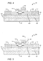
- FiG.4 shows an embodiment of a FET device 400 according to the present invention.
- Device 400 is similar to transistor device 100, comprising many of the same features that are described above including substrate 102, active region 104, barrier layer 106, plurality of semiconductor layers 108, source electrode 110, drain electrode 112 and gate electrode 114.
- This particular embodiment includes first and second spacer layers 402, 404 and a field plate 406. After the epitaxial layers are grown, a first insulating spacer layer 402 is applied to the top surface of the barrier layer 106.
- the spacer layer 402 may comprise SiN or other suitable non-conductive materials as mentioned above. Openings for the gate 114 are then etched into the first spacer layer 402, and the gate 114 is then deposited.
- a second insulating spacer layer 404 comprising SiN, for example, or another suitable material is then deposited, covering the gate 114 and at least part of the surface of the first spacer layer 402.
- Field plate 406 is then deposited on the second spacer layer 404.
- a typical composition for the field plate 406 is Ni/Au/Ni; however other materials may also be used.
- the field plate 406 may be connected to either the source electrode 110 or the gate electrode 114. As discussed above, the field plate 406 operates to reduce field concentrations within the device, improving performance and the operating lifetime of the device.
- FIG.5 shows another embodiment of a FET device 500 according to the present invention.
- the device 500 functions similarly as device 400 and shares several common elements that are described above including substrate 102, active region 104, barrier layer 106, plurality of semiconductor layers 108, source electrode 110, drain electrode 112, gate electrode 114, first and second spacer layers 402, 404 and field plate 906.
- This particular embodiment includes an additional spacer layer 502 and field plate 504.
- Field plate 504 serves to further reduce the electric field at specific points inside the device 500.
- spacer layer 502 and field plate 504 are shown as hashed elements to indicate that the elements are optional. In fact, additional spacer layer/field plate pairs can be included as needed. Each additional field plate may be separated from the previous field plate by an additional spacer layer.
- FIG.6 shows a top-side view of one embodiment of a FET device 600 according to the present invention.
- the field plate 602 can be electrically connected to either the source electrode 110 or the gate 114.
- FIG. 6 shows one embodiment according to the present invention wherein the field plate 602 is connected to the source electrode 110, with two alternative connection structures being shown.
- First conductive buses 604 can be formed on the spacer layer 612 to extend between the field plate 602 and the source electrode 110. Different numbers of buses can be used although the more buses that are used, the greater the unwanted capacitance that can be introduced by the buses.
- the buses 604 should have a sufficient number so that current effectively spreads between the source electrode 110 and the field plate 602, while covering as little cf the FET active region as possible.
- a suitable number of buses 604 can be three as shown in FIG. 6 .
- the field plate 602 can also be electrically connected to the source electrode 110 through a conductive path 606 that runs outside of the active region of the FET 600 and is connected to the source electrode 110. As shown in FIG. 6 , the path 606 runs outside the active area of the FET 600 at the edge opposite the gate contact 608. In alternative embodiments according to the present invention, the conductive path could run outside the active area of the FET on the side of the gate contact 608, or the FET 600 could include two or more conductive paths running on one or both sides of the FET 600. In one embodiment, the conductive paths 604, 606 can be made of the same material as the source electrode 110 and in other embodiments they can be made of a different material and can be formed at a different step in the fabrication process after formation of the source electrode 110.
- the field plate 602 can also be electrically connected to the gate 114 by many different methods, with two suitable methods described herein.
- the field plate can be connected to the gate 114 by a second conductive path 610 that runs outside of the active region of the FET 600 between the field plate 602 and gate 114.
- the conductive path 610 can connect to the gate contact 608 or a portion of the gate 114 outside of the FET active region, such as the portion of the gate 114 opposite the gate contact 608.
- more than one conductive path can be used to connect the field plate 602 and gate 114.
- An alternative connection structure comprises conductive paths in the form of conductive vias (not shown), which can be formed running from the first field plate 602 to the gate 114, through the spacer layer 612.
- the vias provide an electrical connection between the gate 114 and first field plate 602 and the vias can be formed by first forming holes in the spacer layer 612, such as by etching, and then filling the holes with a conductive material either in a separate step or during formation of the field plate 602.
- the vias can be arranged periodically down the first field plate 602 to provide for effective current spreading from the gate 114 to the field plate 602.
- FIG.7 shows a graph detailing the results of an experiment testing the degradation of a transistor device having NiCr (80-20 wt%) as the contact layer and a transistor device having a typical contact layer material such as Ni.
- the graph plots power output (Pout) of the devices in dBm versus time in hours. Both devices were biased with 28V and heated, resulting in an estimated junction temperature of approximately 350°C for close to 100 hours. After stressing the device under the specified conditions, the graph shows the device with the NiCr contact layer sustained a drop in power output of approximately 0.25dBm. The device having the Ni contact layer sustained a drop in power output of more than 1dBm after stressing.
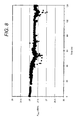
- FIG.8 is a graph of empirical data resulting from an experiment testing the degradation over time of a transistor device having NiCr (30-20 wt%) as the contact layer.
- the device had approximate dimensions of 0.6 ⁇ m in length and 246 ⁇ m in width.
- the graph plot the power output (P out ) in dBm versus time in hours.
- the device was biased with a drain voltage of approximately 28V and heated.
- the base plate temperature was approximately 310°C, resulting in a junction temperature close to 340°C.
- the device was heated for 120 hours with the P out being sampled every two minutes.
- the test was conducted at 4GHz with a compression level of 3dB. The data indicate that after being stressed under the specified conditions for 120 hours the device sustained a drop in P out of less than 0.5dBm.
Abstract
Description
- The invention relates to transistors, and more particularly to transistors designed to operate efficiently at high temperatures.
- Improvements in the manufacturing of AlGaN/GaN semiconductor materials have helped advance the development of AlGaN/GaN transistors, such as high electron mobility transistors (HEMTs) for high frequency, high temperature and high power applications. AlGaN/GaN has large bandgaps, high peak and saturation electron velocity values [B. Gelmont, K. Kim and M. Shur, Monte Carlo Simulation of Electron Transport in Gallium Nitride, J.Appl.Phys. 74, (1993), pp. 1818-1821]. AlGaN/GaN HEMTs can also have 2DEG sheet densities in excess of 1013cm-2 and relatively high electron mobility (up to 2019 cm2/Vs) [R. Gaska, et al., Electron Transport in AlGaN-GaN Heterostructures Grown on 6H-SiC Substrates, Appl.Phys.Lett. 72, (1998), pp. 707-709]. These characteristics allow AlGaN/GaN HEMTs to provide very high voltage and high power operation at RE, microwave and millimeter wave frequencies.
-
U.S. Patent number 5,192,987 to Khan et al. discloses GaN/AlGaN based HEMTs grown on a buffer and a substrate. Other AlGaN/GaN HEMTs and field effect transistors (FETs) have been described by Gaska et al., High-Temperature Performance of AlGaN/GaN HFET's on SiC Substrates, IEEE Electron Device Letters, 18, (1997), pp. 492-494; and Wu et al. "High Al-content AlGaN/GaN HEMTs With Very High Performance", IEDM-1999 Digest, pp. 925-927, Washington DC, Dec. 1999. Some of these devices have shown a gain-bandwidth product (fT) as high as 100 gigahertz (Lu et al. "AlGaN/GaN HEMTs on SiC With Over 100 GHz ft and Low Microwave Noise", IEEE Transactions on Electron Devices, Vol. 48, No. 3, March 2001, pp. 581-585) and high power densities up to 10 W/mm at X-band (Wu et al., "Bias-dependent Performance of High-Power AlGaN/GaN HEMTs", IEDM-2001, Washington DC, Dec. 2-6, 2001). - Electron trapping and the resulting difference between DC and RF characteristics have been a limiting factor in the performance of these devices. Silicon nitride (SiN) passivation has been successfully employed to alleviate this trapping problem resulting in high performance devices with power densities over 10W/mm at 10 Ghz. For example,
U.S. Patent No. 6,586,781 , which is incorporated herein by reference in its entirety, discloses methods and structures for reducing the trapping effect in GaN-based transistors. However, due to the high electric fields existing in these structures, charge trapping is still an issue. - Field plates have been used to enhance the performance of GaN-based HEMTs [See S Kamalkar and U.K. Mishra, Very High Voltage AlGaN/GaN High Electron Mobility Transistors Using a Field Plate Deposited on a Stepped Insulator, Solid State Electronics 45, (2001), pp. 1645-1662]. Recently, field plate optimisation for operation at microwave frequencies has resulted in drastically improved power densities exceeding 30 W/mm at 4 and 8 GHz [Wu et al, 30 W/mm GaN HEMTs by field plate optimization, IEEE Electron Device Letters, Vol. 25, No.3, March 2004]. However, the reliability of these devices is still an issue, especially at high operation temperatures.
- The present invention provides transistors that operate efficiently at high temperatures and exhibit low degradation over time. One embodiment of a transistor device according to the present invention comprises an active region comprising a plurality of semiconductor layers. Source and drain electrodes are formed in contact with the active region. A gate electrode is formed on the active region between the source and drain electrodes. The gate comprises a contact portion made from a material having a high Schottky barrier and exhibiting low degradation at high operating temperatures. The contact portion is disposed to contact the active region. A spacer layer is formed on at least part of the surface of the active region between the source and drain electrodes.
- One embodiment of a field effect transistor (FET) according to the present invention comprises an active region comprising a plurality of semiconductor layers. Drain and source electrodes are formed in contact with the active region. A gate electrode is formed on the active region between the source and drain electrodes. The gate comprises a contact portion made from a material having a high Schottky barrier and exhibiting low degradation at high operating temperatures. The contact portion is disposed to contact the active region. First and second spacer layers are formed. The first spacer layer covers at least part of the surface of the active region. The second spacer layer covers the gate electrode and at least part of the first spacer layer. A field plate is disposed on the second spacer layer.
- One embodiment of a Group-III nitride transistor device according to the present invention comprises an active region comprising a plurality of active semiconductor layers. A source electrode is formed in contact with the active region. A drain electrode is formed in contact with the active region. A gate electrode is formed on the active region between the source and drain electrodes. The gate comprises a contact portion made from a material selected from the group consisting of platinum (Pt), tungsten (W), molybdenum (Mo), chromium (Cr), and nickel-chromium alloys (NiCr). At least one spacer layer is disposed on at least part of the surface of the active region between the source and drain electrodes.
- Another embodiment of a Group-III nitride transistor device according to the present invention comprises an active region comprising a plurality of active semiconductor layers. A source electrode is formed in contact with the active region. A drain electrode is formed in contact with the active region. A gate electrode is formed on the active region between the source and drain electrodes. The gate comprises a contact portion made from polycrystalline indium nitride (InN). At least one spacer layer is disposed on at least part of the surface of the active region between the source and drain electrodes.
-
FIG.1 is a sectional view of one embodiment of a transistor device according to the present invention; -
FIG.2 is a sectional view of one embodiment of the gate of a transistor device according to the present invention; -
FIG.3 is a sectional view of one embodiment of a transistor device according to the present invention; -
FIG.4 is a sectional view of one embodiment of a FET according to the present invention; -
FIG.5 is a sectional view of one embodiment of a FET according to the present invention; -
FIG.6 is a plan view of the top side of a transistor device according to the present invention; and -
FIG.7 is a graph power output versus time for two different gate materials. -
FIG.8 is a graph of power output versus time for a transistor device having a gate electrode with a NiCr contact portion. - The structure and composition of the transistor gate according to the present invention can be used with many different transistor structures, such as high electron mobility transistors (HEMTs). Transistors generally include an active region having a plurality cf semiconductor layers, one of which is a channel layer. Metal source and drain electrodes are formed in contact with the active region, and a gate is formed on the active region between the source and drain electrodes for modulating electric fields within the active region. In one embodiment, a first non-conductive spacer layer is formed above the active region, over at least a portion of the surface of the active region between the source and the drain. In another embodiment, a second non-conductive spacer layer is formed over at least a portion of the first spacer layer and the gate electrode, and a field plate is disposed on the second spacer layer. The spacer layers can comprise a dielectric layer or a combination of multiple dielectric layers, and in certain embodiments other materials such as epitaxially grown layers.
- In one embodiment, a conductive field plate is formed on the second spacer layer with the spacer layer providing isolation between the field plate the active region below. The field plate extends a distance on the spacer layer from the edge of the gate toward the drain electrode, and can extend a distance on the spacer layer toward the source electrode. The field plate can be electrically connected to either the source electrode or the gate. The field plate arrangement can reduce the peak electric field in the device, resulting in increased breakdown voltage and reduced trapping. The reduction of the electric field can also yield other benefits such as reduced leakage currents and enhanced reliability. Additional spacer layer and field plate pairs can also be included.
- The gate electrode can be made of several materials that have a high Schottky barrier corresponding to a specific semiconductor system (e.g., GaN or AlGaN) and exhibit low degradation at high operating temperatures. In the GaN semiconductor system, a high Schottky barrier is considered to be any barrier height in excess of 0.4eV, with a preferred barrier height in excess of 0.45eV. Low degradation at high operating temperatures means that the RF output power of the device degrades by no more than 0.5dB after the device has been operated for 100 hours at 350°C. Various materials have these characteristics when used in certain semiconductor systems. For example, gate electrodes that have certain nickel-chromium alloys (NiCr) as the gate contact metal exhibit improved durability at high operating temperatures. Other materials have exhibited similar results as discussed below.
- It will be understood that when an element or layer is referred to as being "on", "connected to", "coupled to" or "in contact with" another element or layer, it can be directly on, connected or coupled to, or in contact with the other element or layer or intervening elements or layers may be present. In contrast, when an element is referred to as being "directly on," "directly connected to", "directly coupled to" or "directly in contact with" another element or layer, there are no intervening elements or layers present. Likewise, when a first element or layer is referred to as being "in electrical contact with" or "electrically coupled to" a second element or layer, there is an electrical path that permits current flow between the first element cr layer and the second element or layer. The electrical path may include capacitors, coupled inductors, and/or other elements that permit current flow even without direct contact between conductive elements.
- Embodiments of the invention are described herein with reference to cross-sectional view illustrations that are schematic illustrations of idealized embodiments of the invention. As such, variations from the shapes of the illustrations as a result, for example, of manufacturing techniques and/or tolerances are expected. Embodiments of the invention should not be construed as limited to the particular shapes of the regions illustrated herein but are to include deviations in shapes that result, for example, from manufacturing. A region illustrated or described as square or rectangular will typically have rounded or curved features due to normal manufacturing tolerances. Thus, the regions illustrated in the figures are schematic in nature and their shapes are not intended to illustrate the precise shape of a region of a device and are not intended to limit the scope of the invention.
-
FIG.1 shows one embodiment of atransistor device 100 according to the present invention that is preferably Group-III nitride based, although other material systems can also be used. Group-III nitrides refer to those semiconductor compounds formed between nitrogen and the elements in the Group-III of the periodic table, usually aluminum (A1), gallium (Ga), and indium (In). The term also refers to ternary and tertiary compounds such as AlGaN and AlInGaN. - The
transistor device 100 can comprise asubstrate 102 which can be made from silicon carbide, sapphire, spinet, ZnO, silicon, gallium nitride, aluminum nitride, or any other material or combinations of materials capable of supporting growth of a Group-III nitride material. In some embodiments the substrate is eliminated from the finished transistor device. -
Substrate 102 can be made of many different materials with a suitable substrate being a 4H polytype of silicon carbide, although other silicon carbide polytypes can also be used including 3C, 6H and 15R polytypes. Silicon carbide has a very high thermal conductivity so that the total output power of Group-III nitride devices on silicon carbide is not limited by the thermal dissipation of the substrate (as may be the case with some devices formed on sapphire). Also, the availability of silicon carbide substrates provides the capacity for device isolation and reduced parasitic capacitance that make commercial devices possible. SiC substrates are available from Cree, Inc., of Durham, North Carolina and methods for producing them are set forth in the scientific literature as well as in aU.S. Patents, Nos. Re. 34,861 ;4,946,547 ; and5,200,022 . - The
transistor device 100 comprises anactive region 104. Theactive region 104 comprises abarrier layer 106 and a plurality ofsemiconductor layers 108.. The plurality ofsemiconductor layers 108 can include a nucleation layer (not explicitly shown) formed on thesubstrate 102 to reduce the lattice mismatch between thesubstrate 102 and the next layer in thetransistor device 100. The nucleation layer should be approximately 1000 angstroms (Å) thick, although other thicknesses can be used. The nucleation layer can comprise many different materials, with a suitable material being Al3Ga1-3N (0<=z<=1), and can be formed on thesubstrate 102 using known semiconductor growth techniques such as Metal Organic Chemical Vapor Deposition (MOCVD), Hydride Vapor Phase Epitaxy (HVPE), or Molecular Beam Epitaxy (MBE). - The plurality of
semiconductor layers 108 can also comprise a high resistivity buffer layer (not explicitly shown) formed on the nucleation layer. The buffer layer can be made of GaN that is approximately 2µm thick, with part of the buffer layer doped with iron (Fe). Other materials can also be used for the buffer layer such as doped or undoped layers of Group-III nitride materials with a preferred buffer layer made of a Group-III nitride material such as AlxGayIn(1-x-y)N (0<=x<=1, 0<=y<=1, x+y<=1). - A
barrier layer 106 can be formed as the top layer of theactive region 104. Thebarrier layer 106 can comprise doped or undoped layers of Group-III nitride materials. The barrier layer can be made of one or multiple layers of AlxGa1-xN, where x ranges from 0-1, and x can be a function of depth such that thebarrier layer 106 can be a graded layer. In HEMT embodiments, a two-dimensional electron gas (2DEG) is induced at the heterointerface between the plurality ofsemiconductors 108 and thebarrier layer 106. - Metal source and drain
electrodes barrier layer 106. Electric current can flow between the source and drainelectrodes active region 104 when thegate 114 is biased at the appropriate level. The formation of source and drainelectrodes electrodes - An insulating
spacer layer 116, for example a layer of SiN, is applied to the top surface of thebarrier layer 106. Openings for thegate 114 are then etched into thespacer layer 116. The layers comprising thegate 114 are then deposited by e-beam evaporation. Other deposition processes might also be used. Thegate 114 can be made of different materials as discussed in detail below with reference toFIG.2 . The gate 24 can have many different lengths, with a suitable gate length ranging from 0.1 to 2.0 microns (µm), although other gate lengths can also be used. - As shown in
FIG.1 , thespacer layer 116 covers all of thebarrier layer 106 between thegate 114 and source and drainelectrodes spacer layer 116 can comprise a dielectric layer, or a combination of multiple dielectric layers. Different dielectric materials can be used such as a SiN, SiO2, Si, Ge, MgOx, MgNx, ZnO, SiNx, SiOx, alloys or layer sequences thereof. Thespacer layer 116 can be many different thicknesses, with a suitable range of thicknesses being approximately 0.03µm to 0.5µm. -
FIG.2 shows one embodiment of agate electrode 114 according to the present invention.Gate electrode 114 is formed on thefirst spacer layer 116 with a portion ofgate 114 contactingbarrier layer 106. In this particular embodiment, acontact layer 202 of a nickel-chromium alloy (NiCr) contacts thebarrier layer 116. The characteristics of theNiCr contact layer 202 are discussed in detail below. Adiffusion barrier 204 is formed on thecontact layer 202. Alateral conduction layer 206 is formed on thediffusion barrier 204. A protective layer 209 is termed on thelateral conduction layer 206. -
Contact layer 202 directly contacts thebarrier layer 106 of the active region. A suitable contact material should have a high Schottky barrier (or a high potential barrier for non-Schottky junctions, such as semiconductor-semiconductor systems) when operating in conjunction with a particular semiconductor system, such as GaN or AlGaN, and should also exhibit durability at high operating voltages and temperatures. Several materials meet these criteria when used with the Group-III nitride systems, including but not limited to Pt, W, Mo, Cr, InN, and various NiCr alloys. A preferred contact layer material is NiCr, with 80% Ni by weight and 20% Cr by weight. NiCr (80-20 wt%) is the preferred source material that can be used in the process whereby thecontact layer 202 is formed on the device. The actual composition of the material comprising thecontact layer 202 that is formed may vary from the composition of the source material. For example, an NiCr (80-20 wt%) source material can yield a contact layer that has a composition of NiCr (50-50 wt%). NiCr (80-20 wt%) has both the high Schottky barrier associated with Ni (in the Group-III Nitride systems) and the high-temperature durability of Cr. When used in conjunction with GaN, a contact layer formed with NiCr (80-20 wt%) has an approximate barrier height of 0.51eV. The barrier height is increased to 0.6-1eV on an AlGaN HEMT and sustained a degradation in output power of 0.3dB when operating at a junction temperature of 340°C for 120 hours as shown inFIG. 8 (discussed below). In the embodiment shown inFIG. 2 , the NiCr contact layer is approximately 20nm thick; however, other thicknesses may be used in the range of 5-1000nm. -
Diffusion barrier 204 separates thecontact layer 202 from thelateral conduction layer 206. The purpose of the diffusion barrier 2C4 is to prevent or retard the inter-diffusion of thecontact layer 202 and thelateral conduction layer 206. The ideal diffusion barrier is inert with respect to the materials that it separates. In this embodiment, thediffusion barrier 204 comprises a layer of Pt. Other materials including, for example, W, Mo, Ir, Ni and Cr, may be used as diffusion barriers depending on the metals that are to be separated.Diffusion layer 204 is shown having an approximate thickness of 30nm; however, other thicknesses may be used, typically in the range of 10-100nm. -
Lateral conduction layer 206 is formed ondiffusion barrier 204. The lateral conduction layer conducts current from one end of thedevice 100 to the other. BecauseFIG.2 shows a cross section of the device, the direction of the current flow through thelateral conduction layer 206 is primarily in a direction normal to plane of the cross section (i.e., coming out of the paper). Thelateral conduction layer 206 should have a high conductivity and sufficient thickness to facilitate current flow. AlthoughFIG.2 shows alateral conduction layer 206 comprising Au, any material which has a high conductivity may be used, taking into account the adjacent materials.Lateral conduction layer 206 is shown having a thickness of 400nm; however, other thicknesses may be used, typically in the range of 100-2000nm. -
Protective layer 208 is formed onlateral conduction layer 206.Protective layer 208 may be necessary to shield thelateral conduction layer 206 from processes that could damage it. In some embodiments the device is treated with corrosive or otherwise damaging processes. For example, a device may be treated using a dry etch process. Aprotective layer 208 may be used to shield thelateral conduction layer 206. Materials such as nickel, for example, are suitable for this purpose. Other materials that are resistant to ion bombardment and other treatment processes may be used as well.Protective layer 208 is shown inFig.2 as having a thickness of 30nm; however, other thicknesses may be used, typically in the range of 10-100nm. - The
gate 114 is shown inFIG.2 as having a split-level structure. Themiddle region 210 of thegate 114 contacts thebarrier layer 106 and theouter regions 212 on either side of the center region are disposed on the spacer layer. The structure of this particular embodiment is such that theouter regions 212 can function as field plate structures. Field plates are discussed in more detail below. - The gate contact structure and composition as disclosed above can be used for many different purposes in a variety of devices. For example,
FIG.3 shows an embodiment of atransistor device 300 according to the present invention. Thedevice 300 has a similar structure asdevice 100 and shares some common elements that are described above includingsource electrode 110,drain electrode 112,active region 104,barrier layer 106, plurality ofsemiconductor layers 108 andsubstrate 102. One difference is the structure of the gate 3G2. The gate does not have the split-level structure. Rather, theentire gate 302 is disposed on thebarrier layer 106. This embodiment does not include a spacer layer. Otherwise, thedevice 300 functions similarly as thedevice 100 . Thegate 302 has the same layered structure as gate 114 (as shown inFIG.2 ), comprising a contact layer, a diffusion barrier, a lateral conduction layer and a protective layer. -
FiG.4 shows an embodiment of aFET device 400 according to the present invention.Device 400 is similar totransistor device 100, comprising many of the same features that are described above includingsubstrate 102,active region 104,barrier layer 106, plurality ofsemiconductor layers 108,source electrode 110,drain electrode 112 andgate electrode 114. This particular embodiment includes first and second spacer layers 402, 404 and afield plate 406. After the epitaxial layers are grown, a first insulatingspacer layer 402 is applied to the top surface of thebarrier layer 106. Thespacer layer 402 may comprise SiN or other suitable non-conductive materials as mentioned above. Openings for thegate 114 are then etched into thefirst spacer layer 402, and thegate 114 is then deposited. A second insulatingspacer layer 404 comprising SiN, for example, or another suitable material is then deposited, covering thegate 114 and at least part of the surface of thefirst spacer layer 402.Field plate 406 is then deposited on thesecond spacer layer 404. A typical composition for thefield plate 406 is Ni/Au/Ni; however other materials may also be used. Thefield plate 406 may be connected to either thesource electrode 110 or thegate electrode 114. As discussed above, thefield plate 406 operates to reduce field concentrations within the device, improving performance and the operating lifetime of the device. -
FIG.5 shows another embodiment of aFET device 500 according to the present invention. Thedevice 500 functions similarly asdevice 400 and shares several common elements that are described above includingsubstrate 102,active region 104,barrier layer 106, plurality ofsemiconductor layers 108,source electrode 110,drain electrode 112,gate electrode 114, first and second spacer layers 402, 404 and field plate 906. This particular embodiment includes anadditional spacer layer 502 andfield plate 504.Field plate 504 serves to further reduce the electric field at specific points inside thedevice 500. InFIG.5 ,spacer layer 502 andfield plate 504 are shown as hashed elements to indicate that the elements are optional. In fact, additional spacer layer/field plate pairs can be included as needed. Each additional field plate may be separated from the previous field plate by an additional spacer layer. -
FIG.6 shows a top-side view of one embodiment of aFET device 600 according to the present invention. Thefield plate 602 can be electrically connected to either thesource electrode 110 or thegate 114.FIG. 6 shows one embodiment according to the present invention wherein thefield plate 602 is connected to thesource electrode 110, with two alternative connection structures being shown. Firstconductive buses 604 can be formed on thespacer layer 612 to extend between thefield plate 602 and thesource electrode 110. Different numbers of buses can be used although the more buses that are used, the greater the unwanted capacitance that can be introduced by the buses. Thebuses 604 should have a sufficient number so that current effectively spreads between thesource electrode 110 and thefield plate 602, while covering as little cf the FET active region as possible. A suitable number ofbuses 604 can be three as shown inFIG. 6 . - The
field plate 602 can also be electrically connected to thesource electrode 110 through aconductive path 606 that runs outside of the active region of theFET 600 and is connected to thesource electrode 110. As shown inFIG. 6 , thepath 606 runs outside the active area of theFET 600 at the edge opposite thegate contact 608. In alternative embodiments according to the present invention, the conductive path could run outside the active area of the FET on the side of thegate contact 608, or theFET 600 could include two or more conductive paths running on one or both sides of theFET 600. In one embodiment, theconductive paths source electrode 110 and in other embodiments they can be made of a different material and can be formed at a different step in the fabrication process after formation of thesource electrode 110. - The
field plate 602 can also be electrically connected to thegate 114 by many different methods, with two suitable methods described herein. First, the field plate can be connected to thegate 114 by a secondconductive path 610 that runs outside of the active region of theFET 600 between thefield plate 602 andgate 114. Theconductive path 610 can connect to thegate contact 608 or a portion of thegate 114 outside of the FET active region, such as the portion of thegate 114 opposite thegate contact 608. Alternatively, more than one conductive path can be used to connect thefield plate 602 andgate 114. - An alternative connection structure comprises conductive paths in the form of conductive vias (not shown), which can be formed running from the
first field plate 602 to thegate 114, through thespacer layer 612. The vias provide an electrical connection between thegate 114 andfirst field plate 602 and the vias can be formed by first forming holes in thespacer layer 612, such as by etching, and then filling the holes with a conductive material either in a separate step or during formation of thefield plate 602. The vias can be arranged periodically down thefirst field plate 602 to provide for effective current spreading from thegate 114 to thefield plate 602. -
FIG.7 shows a graph detailing the results of an experiment testing the degradation of a transistor device having NiCr (80-20 wt%) as the contact layer and a transistor device having a typical contact layer material such as Ni. The graph plots power output (Pout) of the devices in dBm versus time in hours. Both devices were biased with 28V and heated, resulting in an estimated junction temperature of approximately 350°C for close to 100 hours. After stressing the device under the specified conditions, the graph shows the device with the NiCr contact layer sustained a drop in power output of approximately 0.25dBm. The device having the Ni contact layer sustained a drop in power output of more than 1dBm after stressing. -
FIG.8 is a graph of empirical data resulting from an experiment testing the degradation over time of a transistor device having NiCr (30-20 wt%) as the contact layer. The device had approximate dimensions of 0.6µm in length and 246µm in width. The graph plot the power output (Pout) in dBm versus time in hours. The device was biased with a drain voltage of approximately 28V and heated. The base plate temperature was approximately 310°C, resulting in a junction temperature close to 340°C. The device was heated for 120 hours with the Pout being sampled every two minutes. The test was conducted at 4GHz with a compression level of 3dB. The data indicate that after being stressed under the specified conditions for 120 hours the device sustained a drop in Pout of less than 0.5dBm. - Although the present invention has been described in detail with reference to certain preferred configurations thereof, other versions are possible. Therefore, the spirit and scope of the invention should not be limited to the versions described above.
Claims (12)
- A transistor device, comprising:an active region comprising a plurality of active semiconductor layers;a source electrode formed in contact with said active region;a drain electrode formed in contact with said active region;a gate electrode formed on said active region between said source and drain electrodes, said gate comprising a contact portion made from a material having a high Schottky barrier and exhibiting low degradation at high operating temperatures, said contact portion disposed to contact said active region; anda first spacer layer disposed on at least part of the surface of said active region between said source and drain electrodes.
- The transistor device of claim 1, wherein said contact portion comprises a nickel-chromium alloy (NiCr) portion.
- The transistor device of claim 2, wherein said NiCr portion comprises more than zero percent (0%) chromium and not more than ninety percent (90%) chromium.
- The transistor device of claim 2, wherein said NiCr portion comprises approximately eighty percent (80%) nickel by weight and approximately twenty percent (20%) chromium by weight.
- The transistor device of claim 2, wherein said NiCr portion comprises approximately fifty percent (50%) nickel by weight and approximately fifty percent (50%) chromium by weight.
- The transistor device of claim 2, wherein said NiCr portion has a thickness of not less than 5nm and not more than 100nm.
- The transistor device of claim 2, wherein said NiCr portion has a thickness of approximately 20nm.
- The transistor device of claim 1, said gate electrode further comprising:a diffusion barrier disposed on said contact portion, such that said contact portion is interposed between said diffusion barrier and said active region;a lateral conduction layer disposed on said diffusion barrier; anda protective layer disposed on said lateral conduction layer.
- The transistor device of claim 1, wherein said transistor device comprises a gallium nitride (GaN) based high electron mobility transistor (HEMT).
- The transistor device of claim 1, wherein said first spacer layer comprises an insulating silicon nitride (SiN) layer.
- The transistor device of claim 1, wherein said contact portion comprises a material selected from the group consisting of platinum (Pt), tungsten (W), molybdenum (Mo), chromium (Cr), nickel-chromium alloys (NiCr), and polycrystalline indium nitride (InN).
- The transistor device of claim 1, further comprising:a second spacer layer covering said gate electrode and at least part of said first spacer layer; anda field plate disposed on said second spacer layer.
Priority Applications (1)
| Application Number | Priority Date | Filing Date | Title |
|---|---|---|---|
| EP11176492.4A EP2385558B1 (en) | 2007-03-23 | 2008-01-16 | High Temperature Performance Capable Gallium Nitride Transistor |
Applications Claiming Priority (1)
| Application Number | Priority Date | Filing Date | Title |
|---|---|---|---|
| US11/726,975 US8212290B2 (en) | 2007-03-23 | 2007-03-23 | High temperature performance capable gallium nitride transistor |
Related Child Applications (3)
| Application Number | Title | Priority Date | Filing Date |
|---|---|---|---|
| EP11176492.4A Division-Into EP2385558B1 (en) | 2007-03-23 | 2008-01-16 | High Temperature Performance Capable Gallium Nitride Transistor |
| EP11176492.4A Division EP2385558B1 (en) | 2007-03-23 | 2008-01-16 | High Temperature Performance Capable Gallium Nitride Transistor |
| EP11176492.4 Division-Into | 2011-08-03 |
Publications (4)
| Publication Number | Publication Date |
|---|---|
| EP1973163A2 true EP1973163A2 (en) | 2008-09-24 |
| EP1973163A3 EP1973163A3 (en) | 2008-12-10 |
| EP1973163B1 EP1973163B1 (en) | 2012-04-11 |
| EP1973163B2 EP1973163B2 (en) | 2015-11-18 |
Family
ID=39529622
Family Applications (2)
| Application Number | Title | Priority Date | Filing Date |
|---|---|---|---|
| EP08250197.4A Active EP1973163B2 (en) | 2007-03-23 | 2008-01-16 | High temperature performance capable gallium nitride transistor |
| EP11176492.4A Active EP2385558B1 (en) | 2007-03-23 | 2008-01-16 | High Temperature Performance Capable Gallium Nitride Transistor |
Family Applications After (1)
| Application Number | Title | Priority Date | Filing Date |
|---|---|---|---|
| EP11176492.4A Active EP2385558B1 (en) | 2007-03-23 | 2008-01-16 | High Temperature Performance Capable Gallium Nitride Transistor |
Country Status (3)
| Country | Link |
|---|---|
| US (2) | US8212290B2 (en) |
| EP (2) | EP1973163B2 (en) |
| JP (2) | JP5203727B2 (en) |
Cited By (9)
| Publication number | Priority date | Publication date | Assignee | Title |
|---|---|---|---|---|
| WO2011014951A1 (en) * | 2009-08-04 | 2011-02-10 | John Roberts | Island matrixed gallium nitride microwave and power switching transistors |
| CN103745993A (en) * | 2014-01-22 | 2014-04-23 | 西安电子科技大学 | Super-junction-based AlGaN/GaN MIS-HEMT (Metal-Insulator-Semiconductor High-Electron-Mobility Transistor) high-voltage device and fabrication method thereof |
| CN103745992A (en) * | 2014-01-22 | 2014-04-23 | 西安电子科技大学 | Composite drain-based AlGaN/GaN MIS-HEMT (Metal-Insulator-Semiconductor High-Electron-Mobility Transistor) high-voltage device and fabrication method thereof |
| CN103745990A (en) * | 2014-01-22 | 2014-04-23 | 西安电子科技大学 | Depletion algan/gan mishemt high voltage device and manufacturing method thereof |
| CN103779412A (en) * | 2014-01-22 | 2014-05-07 | 西安电子科技大学 | High-voltage device based on depletion mode and manufacturing method of high-voltage device |
| CN103839996A (en) * | 2014-01-22 | 2014-06-04 | 西安电子科技大学 | Groove grid high-voltage device based on composite drain electrode and method for manufacturing same |
| US8791508B2 (en) | 2010-04-13 | 2014-07-29 | Gan Systems Inc. | High density gallium nitride devices using island topology |
| US9818857B2 (en) | 2009-08-04 | 2017-11-14 | Gan Systems Inc. | Fault tolerant design for large area nitride semiconductor devices |
| CN114068682A (en) * | 2020-07-29 | 2022-02-18 | 格芯(美国)集成电路科技有限公司 | Symmetrical arrangement of field plates in semiconductor devices |
Families Citing this family (35)
| Publication number | Priority date | Publication date | Assignee | Title |
|---|---|---|---|---|
| US9773877B2 (en) | 2004-05-13 | 2017-09-26 | Cree, Inc. | Wide bandgap field effect transistors with source connected field plates |
| US11791385B2 (en) | 2005-03-11 | 2023-10-17 | Wolfspeed, Inc. | Wide bandgap transistors with gate-source field plates |
| US8035130B2 (en) * | 2007-03-26 | 2011-10-11 | Mitsubishi Electric Corporation | Nitride semiconductor heterojunction field effect transistor having wide band gap barrier layer that includes high concentration impurity region |
| JP2010199241A (en) * | 2009-02-24 | 2010-09-09 | Fujitsu Ltd | Semiconductor device |
| JP5595685B2 (en) * | 2009-07-28 | 2014-09-24 | パナソニック株式会社 | Semiconductor device |
| US9029866B2 (en) | 2009-08-04 | 2015-05-12 | Gan Systems Inc. | Gallium nitride power devices using island topography |
| US20110049569A1 (en) * | 2009-09-02 | 2011-03-03 | International Rectifier Corporation | Semiconductor structure including a field modulation body and method for fabricating same |
| TWI380377B (en) * | 2009-12-23 | 2012-12-21 | Intersil Inc | Methods for manufacturing enhancement-mode hemts with self-aligned field plate |
| JP2011187623A (en) * | 2010-03-08 | 2011-09-22 | Furukawa Electric Co Ltd:The | Semiconductor element and manufacturing method thereof |
| JP5666157B2 (en) * | 2010-03-26 | 2015-02-12 | パナソニック株式会社 | Bidirectional switch element and bidirectional switch circuit using the same |
| JP5685020B2 (en) * | 2010-07-23 | 2015-03-18 | 住友電気工業株式会社 | Manufacturing method of semiconductor device |
| US8513703B2 (en) | 2010-10-20 | 2013-08-20 | National Semiconductor Corporation | Group III-nitride HEMT with multi-layered substrate having a second layer of one conductivity type touching a top surface of a first layers of different conductivity type and a method for forming the same |
| US8502273B2 (en) * | 2010-10-20 | 2013-08-06 | National Semiconductor Corporation | Group III-nitride HEMT having a well region formed on the surface of substrate and contacted the buffer layer to increase breakdown voltage and the method for forming the same |
| JP2012175089A (en) * | 2011-02-24 | 2012-09-10 | Fujitsu Ltd | Semiconductor device and method of manufacturing semiconductor device |
| US9024357B2 (en) * | 2011-04-15 | 2015-05-05 | Stmicroelectronics S.R.L. | Method for manufacturing a HEMT transistor and corresponding HEMT transistor |
| CN102856361B (en) * | 2011-06-29 | 2015-07-01 | 财团法人工业技术研究院 | Transistor element with double-sided field plate and manufacturing method thereof |
| JP5908692B2 (en) * | 2011-09-29 | 2016-04-26 | トランスフォーム・ジャパン株式会社 | Compound semiconductor device and manufacturing method thereof |
| KR101869045B1 (en) * | 2012-01-11 | 2018-06-19 | 삼성전자 주식회사 | High electron mobility transistor and method of manufacturing the same |
| JP5995309B2 (en) * | 2012-03-28 | 2016-09-21 | 住友電工デバイス・イノベーション株式会社 | Semiconductor device and manufacturing method thereof |
| US8860091B2 (en) | 2012-04-16 | 2014-10-14 | Hrl Laboratories, Llc | Group III-N HFET with a graded barrier layer |
| JP5983999B2 (en) | 2012-06-29 | 2016-09-06 | 住友電工デバイス・イノベーション株式会社 | Manufacturing method of semiconductor device |
| US9755059B2 (en) | 2013-06-09 | 2017-09-05 | Cree, Inc. | Cascode structures with GaN cap layers |
| US9847411B2 (en) * | 2013-06-09 | 2017-12-19 | Cree, Inc. | Recessed field plate transistor structures |
| US9905658B2 (en) | 2013-11-26 | 2018-02-27 | Nxp Usa, Inc. | Transistors with field plates resistant to field plate material migration and methods of their fabrication |
| JP6135487B2 (en) | 2013-12-09 | 2017-05-31 | 富士通株式会社 | Semiconductor device and manufacturing method of semiconductor device |
| CN103779411B (en) * | 2014-01-22 | 2017-01-25 | 西安电子科技大学 | High voltage device based on super junction groove gates and manufacturing method of high voltage device |
| US20150263116A1 (en) * | 2014-03-14 | 2015-09-17 | Chunong Qiu | High electron mobility transistors with improved gates and reduced surface traps |
| US20150372096A1 (en) * | 2014-06-20 | 2015-12-24 | Ishiang Shih | High Electron Mobility Transistors and Integrated Circuits with Improved Feature Uniformity and Reduced defects for Microwave and Millimetre Wave Applications |
| JP2017059621A (en) * | 2015-09-15 | 2017-03-23 | 三菱電機株式会社 | Semiconductor device and manufacturing method for the same |
| US10056478B2 (en) | 2015-11-06 | 2018-08-21 | Taiwan Semiconductor Manufacturing Company Ltd. | High-electron-mobility transistor and manufacturing method thereof |
| US11508821B2 (en) * | 2017-05-12 | 2022-11-22 | Analog Devices, Inc. | Gallium nitride device for high frequency and high power applications |
| JP6978151B2 (en) * | 2017-09-28 | 2021-12-08 | 住友電工デバイス・イノベーション株式会社 | Manufacturing method of semiconductor device and semiconductor device |
| IT201900019980A1 (en) * | 2019-10-29 | 2021-04-29 | St Microelectronics Srl | METHOD OF MANUFACTURING A PORT TERMINAL OF A HEMT DEVICE, AND A HEMT DEVICE |
| RU209181U1 (en) * | 2021-09-29 | 2022-02-04 | Федеральное государственное автономное образовательное учреждение высшего образования "Национальный исследовательский университет "Московский институт электронной техники" | HIGH-VOLTAGE LATERAL GALLIUM NITRIDE TRANSISTOR FOR LOW-INDUCTIVE CASCODE CIRCUITS |
| CN114586176B (en) * | 2021-12-31 | 2024-01-23 | 英诺赛科(苏州)半导体有限公司 | Nitrogen-based bidirectional switch device and manufacturing method thereof |
Citations (5)
| Publication number | Priority date | Publication date | Assignee | Title |
|---|---|---|---|---|
| US4946547A (en) | 1989-10-13 | 1990-08-07 | Cree Research, Inc. | Method of preparing silicon carbide surfaces for crystal growth |
| US5192987A (en) | 1991-05-17 | 1993-03-09 | Apa Optics, Inc. | High electron mobility transistor with GaN/Alx Ga1-x N heterojunctions |
| US5200022A (en) | 1990-10-03 | 1993-04-06 | Cree Research, Inc. | Method of improving mechanically prepared substrate surfaces of alpha silicon carbide for deposition of beta silicon carbide thereon and resulting product |
| USRE34861E (en) | 1987-10-26 | 1995-02-14 | North Carolina State University | Sublimation of silicon carbide to produce large, device quality single crystals of silicon carbide |
| US6586781B2 (en) | 2000-02-04 | 2003-07-01 | Cree Lighting Company | Group III nitride based FETs and HEMTs with reduced trapping and method for producing the same |
Family Cites Families (90)
| Publication number | Priority date | Publication date | Assignee | Title |
|---|---|---|---|---|
| BE792908A (en) | 1971-12-20 | 1973-04-16 | Western Electric Co | PROCESS FOR MANUFACTURING SEMICONDUCTOR DEVICES |
| JPS51129173A (en) | 1974-02-01 | 1976-11-10 | Chisso Corp | Semi conductor with high voltage proof schottky electrode and it's man uacturing method. |
| JPS5360567A (en) | 1976-11-11 | 1978-05-31 | Mitsubishi Electric Corp | Electrode formation method of semiconductor device |
| JPS5539636A (en) | 1978-09-13 | 1980-03-19 | Nec Corp | Composite semiconductor |
| DE3323347A1 (en) | 1983-06-29 | 1985-01-10 | Neff Gewindespindeln GmbH, 7035 Waldenbuch | BALL REAR SCREW GEAR |
| JPS63188964A (en) | 1987-01-31 | 1988-08-04 | Dainippon Printing Co Ltd | Integrated circuit package |
| DE3823347A1 (en) † | 1988-07-09 | 1990-01-11 | Semikron Elektronik Gmbh | Power semiconductor element |
| EP0391380B1 (en) | 1989-04-04 | 1997-12-17 | Siemens Aktiengesellschaft | HEMT Structure |
| JP2912635B2 (en) | 1989-08-04 | 1999-06-28 | 富士通株式会社 | Semiconductor device |
| US5252843A (en) | 1989-09-01 | 1993-10-12 | Fujitsu Limited | Semiconductor device having overlapping conductor layers |
| JPH0446527A (en) | 1990-06-11 | 1992-02-17 | Fuji Electric Co Ltd | Controlling method for current of harmonic wave suppressor |
| JP2702338B2 (en) | 1991-10-14 | 1998-01-21 | 三菱電機株式会社 | Semiconductor device and manufacturing method thereof |
| JP3019885B2 (en) | 1991-11-25 | 2000-03-13 | カシオ計算機株式会社 | Method for manufacturing field effect thin film transistor |
| JPH05326890A (en) | 1992-05-07 | 1993-12-10 | Nec Corp | Output buffer circuit |
| EP0569745A1 (en) | 1992-05-14 | 1993-11-18 | Siemens Aktiengesellschaft | Method of manufacturing a field effect transistor with asymmetrical gate structure |
| JPH06124965A (en) | 1992-10-09 | 1994-05-06 | Sumitomo Electric Ind Ltd | Field effect transistor |
| JPH07283140A (en) | 1994-04-05 | 1995-10-27 | Nippon Telegr & Teleph Corp <Ntt> | Active atom feeding control method |
| JPH07326737A (en) | 1994-05-31 | 1995-12-12 | Nippon Steel Corp | Impedance line, filter element, delay element and semiconductor device |
| GB2296373B (en) | 1994-12-14 | 1997-09-10 | Toshiba Cambridge Res Center | Semiconductor device |
| JPH08264760A (en) | 1995-03-23 | 1996-10-11 | Mitsubishi Electric Corp | Hetero junction field-effect transistor and its manufacture |
| US5670798A (en) | 1995-03-29 | 1997-09-23 | North Carolina State University | Integrated heterostructures of Group III-V nitride semiconductor materials including epitaxial ohmic contact non-nitride buffer layer and methods of fabricating same |
| JP3449116B2 (en) | 1996-05-16 | 2003-09-22 | ソニー株式会社 | Semiconductor device |
| JP3376211B2 (en) | 1996-05-29 | 2003-02-10 | 株式会社東芝 | Semiconductor device, method of manufacturing semiconductor substrate, and method of manufacturing semiconductor device |
| US5920105A (en) | 1996-09-19 | 1999-07-06 | Fujitsu Limited | Compound semiconductor field effect transistor having an amorphous gas gate insulation layer |
| US5930656A (en) | 1996-10-21 | 1999-07-27 | Kabushiki Kaisha Toshiba | Method of fabricating a compound semiconductor device |
| JPH10223901A (en) | 1996-12-04 | 1998-08-21 | Sony Corp | Field effect transistor and manufacture of the same |
| JPH10173036A (en) | 1996-12-11 | 1998-06-26 | Nec Corp | Semiconductor device and method of realizing high-resistance semiconductor |
| JPH10189565A (en) | 1996-12-26 | 1998-07-21 | Tokyo Electron Ltd | Wafer board |
| US6004881A (en) | 1997-04-24 | 1999-12-21 | The United States Of America As Represented By The Secretary Of The Air Force | Digital wet etching of semiconductor materials |
| JP3147036B2 (en) | 1997-05-02 | 2001-03-19 | 日本電気株式会社 | Compound semiconductor device and method of manufacturing the same |
| JPH10335637A (en) | 1997-05-30 | 1998-12-18 | Sony Corp | Hetero-junction field effect transistor |
| US6316820B1 (en) | 1997-07-25 | 2001-11-13 | Hughes Electronics Corporation | Passivation layer and process for semiconductor devices |
| JP3161516B2 (en) | 1997-10-03 | 2001-04-25 | 日本電気株式会社 | Method for manufacturing semiconductor device |
| US5966597A (en) | 1998-01-06 | 1999-10-12 | Altera Corporation | Method of forming low resistance gate electrodes |
| JP3372470B2 (en) | 1998-01-20 | 2003-02-04 | シャープ株式会社 | Nitride III-V compound semiconductor device |
| JPH11261051A (en) | 1998-03-09 | 1999-09-24 | Nippon Telegr & Teleph Corp <Ntt> | Semiconductor device |
| JP3439111B2 (en) | 1998-03-09 | 2003-08-25 | 古河電気工業株式会社 | High mobility transistor |
| US6316793B1 (en) | 1998-06-12 | 2001-11-13 | Cree, Inc. | Nitride based transistors on semi-insulating silicon carbide substrates |
| JP2000068498A (en) | 1998-08-21 | 2000-03-03 | Nippon Telegr & Teleph Corp <Ntt> | Insulating nitride film and semiconductor device using the same |
| US6720589B1 (en) * | 1998-09-16 | 2004-04-13 | Kabushiki Kaisha Toshiba | Semiconductor device |
| JP4182376B2 (en) | 1998-12-02 | 2008-11-19 | 富士通株式会社 | Semiconductor device |
| JP3180907B2 (en) * | 1998-12-17 | 2001-07-03 | 日本電気株式会社 | Field effect transistor and method of manufacturing the same |
| JP3209270B2 (en) | 1999-01-29 | 2001-09-17 | 日本電気株式会社 | Heterojunction field effect transistor |
| JP4224737B2 (en) | 1999-03-04 | 2009-02-18 | ソニー株式会社 | Semiconductor element |
| JP2000266117A (en) | 1999-03-15 | 2000-09-26 | Kosuke Nagaya | Rotary magnetic damper |
| JP2001007325A (en) | 1999-06-18 | 2001-01-12 | Sanyo Electric Co Ltd | Field-effect transistor |
| JP3710339B2 (en) | 1999-08-31 | 2005-10-26 | シャープ株式会社 | GaN compound semiconductor light emitting device manufacturing method |
| JP2001085670A (en) | 1999-09-14 | 2001-03-30 | Nec Corp | Field effect type transistor and its manufacturing method |
| JP3414678B2 (en) | 1999-09-29 | 2003-06-09 | 三容真空工業株式会社 | Sputtering method and apparatus |
| JP2001251869A (en) | 2000-03-01 | 2001-09-14 | Osaka Gas Co Ltd | Dc/ac conversion circuit, power converter and power generating system |
| US6686616B1 (en) * | 2000-05-10 | 2004-02-03 | Cree, Inc. | Silicon carbide metal-semiconductor field effect transistors |
| JP2002077353A (en) | 2000-08-25 | 2002-03-15 | Moriguchi:Kk | Structure for attachment of light-emitting device for communications equipment to communications equipment |
| JP3708810B2 (en) | 2000-09-01 | 2005-10-19 | シャープ株式会社 | Nitride III-V compound semiconductor device |
| DE60224010T2 (en) † | 2001-01-23 | 2008-12-04 | Société de Technologie Michelin | HANGING DEVICE FOR A MOTORCYCLE WHEEL |
| US20020173062A1 (en) † | 2001-05-17 | 2002-11-21 | Lung-Chien Chen | Method for manufacturing GaN-based LED |
| US6794719B2 (en) | 2001-06-28 | 2004-09-21 | Koninklijke Philips Electronics N.V. | HV-SOI LDMOS device with integrated diode to improve reliability and avalanche ruggedness |
| US7230284B2 (en) | 2001-07-24 | 2007-06-12 | Cree, Inc. | Insulating gate AlGaN/GaN HEMT |
| JP2003100778A (en) | 2001-09-26 | 2003-04-04 | Toshiba Corp | Semiconductor device |
| US6833564B2 (en) | 2001-11-02 | 2004-12-21 | Lumileds Lighting U.S., Llc | Indium gallium nitride separate confinement heterostructure light emitting devices |
| JP2003209124A (en) * | 2001-11-06 | 2003-07-25 | Sony Corp | Method of manufacturing field-effect semiconductor device, and field-effect semiconductor device |
| JP3705431B2 (en) | 2002-03-28 | 2005-10-12 | ユーディナデバイス株式会社 | Semiconductor device and manufacturing method thereof |
| JP3952383B2 (en) | 2002-05-21 | 2007-08-01 | 富士通株式会社 | Compound field effect semiconductor device |
| JP4221697B2 (en) | 2002-06-17 | 2009-02-12 | 日本電気株式会社 | Semiconductor device |
| US6933544B2 (en) | 2003-01-29 | 2005-08-23 | Kabushiki Kaisha Toshiba | Power semiconductor device |
| CN100388509C (en) | 2003-01-29 | 2008-05-14 | 株式会社东芝 | Power semiconductor device |
| US7078743B2 (en) † | 2003-05-15 | 2006-07-18 | Matsushita Electric Industrial Co., Ltd. | Field effect transistor semiconductor device |
| US7501669B2 (en) | 2003-09-09 | 2009-03-10 | Cree, Inc. | Wide bandgap transistor devices with field plates |
| JP2005086171A (en) | 2003-09-11 | 2005-03-31 | Fujitsu Ltd | Semiconductor device and method of fabricating same |
| JP4417677B2 (en) | 2003-09-19 | 2010-02-17 | 株式会社東芝 | Power semiconductor device |
| US7071498B2 (en) | 2003-12-17 | 2006-07-04 | Nitronex Corporation | Gallium nitride material devices including an electrode-defining layer and methods of forming the same |
| US7170111B2 (en) | 2004-02-05 | 2007-01-30 | Cree, Inc. | Nitride heterojunction transistors having charge-transfer induced energy barriers and methods of fabricating the same |
| US7465997B2 (en) * | 2004-02-12 | 2008-12-16 | International Rectifier Corporation | III-nitride bidirectional switch |
| GB2412009B (en) | 2004-03-11 | 2006-01-25 | Toshiba Research Europ Limited | A semiconductor device and method of its manufacture |
| US7573078B2 (en) * | 2004-05-11 | 2009-08-11 | Cree, Inc. | Wide bandgap transistors with multiple field plates |
| US7550783B2 (en) | 2004-05-11 | 2009-06-23 | Cree, Inc. | Wide bandgap HEMTs with source connected field plates |
| US7432142B2 (en) | 2004-05-20 | 2008-10-07 | Cree, Inc. | Methods of fabricating nitride-based transistors having regrown ohmic contact regions |
| WO2005114713A1 (en) | 2004-05-21 | 2005-12-01 | Matsushita Electric Industrial Co., Ltd. | Impurity introducing method and electronic element using it |
| JP4682541B2 (en) | 2004-06-15 | 2011-05-11 | 豊田合成株式会社 | Semiconductor crystal growth method |
| JP4810072B2 (en) | 2004-06-15 | 2011-11-09 | 株式会社東芝 | Nitrogen compound-containing semiconductor devices |
| JP4379305B2 (en) | 2004-11-09 | 2009-12-09 | サンケン電気株式会社 | Semiconductor device |
| JP4866007B2 (en) | 2005-01-14 | 2012-02-01 | 富士通株式会社 | Compound semiconductor device |
| US11791385B2 (en) * | 2005-03-11 | 2023-10-17 | Wolfspeed, Inc. | Wide bandgap transistors with gate-source field plates |
| US7365374B2 (en) | 2005-05-03 | 2008-04-29 | Nitronex Corporation | Gallium nitride material structures including substrates and methods associated with the same |
| EP1901342A4 (en) | 2005-06-10 | 2009-07-22 | Nec Corp | Field effect transistor |
| EP1901341A4 (en) | 2005-06-10 | 2009-07-15 | Nec Corp | Field effect transistor |
| TW200715570A (en) | 2005-09-07 | 2007-04-16 | Cree Inc | Robust transistors with fluorine treatment |
| JP5231719B2 (en) * | 2006-03-30 | 2013-07-10 | 富士通株式会社 | Method for manufacturing field effect transistor |
| US7703945B2 (en) | 2006-06-27 | 2010-04-27 | Cree, Inc. | Efficient emitting LED package and method for efficiently emitting light |
| US7692263B2 (en) | 2006-11-21 | 2010-04-06 | Cree, Inc. | High voltage GaN transistors |
| US7585329B2 (en) | 2006-11-28 | 2009-09-08 | Depuy Products, Inc. | Modular proximal body trial |
-
2007
- 2007-03-23 US US11/726,975 patent/US8212290B2/en active Active
-
2008
- 2008-01-16 EP EP08250197.4A patent/EP1973163B2/en active Active
- 2008-01-16 EP EP11176492.4A patent/EP2385558B1/en active Active
- 2008-01-23 JP JP2008013133A patent/JP5203727B2/en active Active
-
2012
- 2012-05-24 US US13/480,328 patent/US9240473B2/en active Active
-
2013
- 2013-02-13 JP JP2013025681A patent/JP2013141000A/en active Pending
Patent Citations (5)
| Publication number | Priority date | Publication date | Assignee | Title |
|---|---|---|---|---|
| USRE34861E (en) | 1987-10-26 | 1995-02-14 | North Carolina State University | Sublimation of silicon carbide to produce large, device quality single crystals of silicon carbide |
| US4946547A (en) | 1989-10-13 | 1990-08-07 | Cree Research, Inc. | Method of preparing silicon carbide surfaces for crystal growth |
| US5200022A (en) | 1990-10-03 | 1993-04-06 | Cree Research, Inc. | Method of improving mechanically prepared substrate surfaces of alpha silicon carbide for deposition of beta silicon carbide thereon and resulting product |
| US5192987A (en) | 1991-05-17 | 1993-03-09 | Apa Optics, Inc. | High electron mobility transistor with GaN/Alx Ga1-x N heterojunctions |
| US6586781B2 (en) | 2000-02-04 | 2003-07-01 | Cree Lighting Company | Group III nitride based FETs and HEMTs with reduced trapping and method for producing the same |
Non-Patent Citations (8)
| Title |
|---|
| B. GELMONT; K. KIM; M. SHUR: "Monte Carlo Simulation of Electron Transport in Gallium Nitride", J.APPL.PHYS., vol. 74, 1993, pages 1818 - 1821, XP008107305, DOI: doi:10.1063/1.354787 |
| GASKA ET AL.: "High-Temperature Performance of AlGaN/GaN HFET's on SiC Substrates", IEEE ELECTRON DEVICE LETTERS, vol. 18, 1997, pages 492 - 494, XP000702977, DOI: doi:10.1109/55.624930 |
| LU ET AL.: "AlGaN/GaN HEMTs on SiC With Over 100 GHz ft and Low Microwave Noise", IEEE TRANSACTIONS ON ELECTRON DEVICES, vol. 48, no. 3, March 2001 (2001-03-01), pages 581 - 585 |
| R. GASKA ET AL.: "Electron Transport in AlGaN-GaN Heterostructures Grown on 6H-SiC Substrates", APPL.PHYS.LETT., vol. 72, 1998, pages 707 - 709, XP012020688, DOI: doi:10.1063/1.120852 |
| S KAMALKAR; U.K. MISHRA: "Very High Voltage AlGaN/GaN High Electron Mobility Transistors Using a Field Plate Deposited cn a Stepped Insulator", SOLID STATE ELECTRONICS, vol. 45, 2001, pages 1645 - 1662 |
| WU ET AL.: "30 W/mm GaN HEMTs by field plate optimization", IEEE ELECTRON DEVICE LETTERS, vol. 25, no. 3, March 2004 (2004-03-01) |
| WU ET AL.: "Bias-dependent Performance of High-Power AlGaN/GaN HEMTs", IEDM-2001, 2 December 2001 (2001-12-02) |
| WU ET AL.: "High Al-content AlGaN/GaN HEMTs With Very High Performance", IEDM-1999 DIGEST, December 1999 (1999-12-01), pages 925 - 927, XP032399403, DOI: doi:10.1109/IEDM.1999.824300 |
Cited By (15)
| Publication number | Priority date | Publication date | Assignee | Title |
|---|---|---|---|---|
| US9818857B2 (en) | 2009-08-04 | 2017-11-14 | Gan Systems Inc. | Fault tolerant design for large area nitride semiconductor devices |
| US9064947B2 (en) | 2009-08-04 | 2015-06-23 | Gan Systems Inc. | Island matrixed gallium nitride microwave and power switching transistors |
| WO2011014951A1 (en) * | 2009-08-04 | 2011-02-10 | John Roberts | Island matrixed gallium nitride microwave and power switching transistors |
| US8791508B2 (en) | 2010-04-13 | 2014-07-29 | Gan Systems Inc. | High density gallium nitride devices using island topology |
| CN103745990A (en) * | 2014-01-22 | 2014-04-23 | 西安电子科技大学 | Depletion algan/gan mishemt high voltage device and manufacturing method thereof |
| CN103839996A (en) * | 2014-01-22 | 2014-06-04 | 西安电子科技大学 | Groove grid high-voltage device based on composite drain electrode and method for manufacturing same |
| CN103779412A (en) * | 2014-01-22 | 2014-05-07 | 西安电子科技大学 | High-voltage device based on depletion mode and manufacturing method of high-voltage device |
| CN103745992A (en) * | 2014-01-22 | 2014-04-23 | 西安电子科技大学 | Composite drain-based AlGaN/GaN MIS-HEMT (Metal-Insulator-Semiconductor High-Electron-Mobility Transistor) high-voltage device and fabrication method thereof |
| CN103745990B (en) * | 2014-01-22 | 2016-03-02 | 西安电子科技大学 | Depletion-mode AlGaN/GaN MISHEMT high tension apparatus and preparation method thereof |
| CN103745993B (en) * | 2014-01-22 | 2016-04-13 | 西安电子科技大学 | Based on the AlGaN/GaN MISHEMT high tension apparatus and preparation method thereof of superjunction |
| CN103745992B (en) * | 2014-01-22 | 2016-05-25 | 西安电子科技大学 | AlGaN/GaN MISHEMT high tension apparatus based on compound drain electrode and preparation method thereof |
| CN103839996B (en) * | 2014-01-22 | 2016-08-17 | 西安电子科技大学 | Groove grid high tension apparatus based on compound drain electrode and preparation method thereof |
| CN103779412B (en) * | 2014-01-22 | 2016-08-17 | 西安电子科技大学 | A kind of based on depletion type high tension apparatus and preparation method thereof |
| CN103745993A (en) * | 2014-01-22 | 2014-04-23 | 西安电子科技大学 | Super-junction-based AlGaN/GaN MIS-HEMT (Metal-Insulator-Semiconductor High-Electron-Mobility Transistor) high-voltage device and fabrication method thereof |
| CN114068682A (en) * | 2020-07-29 | 2022-02-18 | 格芯(美国)集成电路科技有限公司 | Symmetrical arrangement of field plates in semiconductor devices |
Also Published As
| Publication number | Publication date |
|---|---|
| US20120228675A1 (en) | 2012-09-13 |
| US9240473B2 (en) | 2016-01-19 |
| JP2008244433A (en) | 2008-10-09 |
| EP2385558A3 (en) | 2013-08-21 |
| EP1973163A3 (en) | 2008-12-10 |
| JP5203727B2 (en) | 2013-06-05 |
| US20080230786A1 (en) | 2008-09-25 |
| EP1973163B1 (en) | 2012-04-11 |
| EP1973163B2 (en) | 2015-11-18 |
| EP2385558A2 (en) | 2011-11-09 |
| US8212290B2 (en) | 2012-07-03 |
| JP2013141000A (en) | 2013-07-18 |
| EP2385558B1 (en) | 2017-10-11 |
Similar Documents
| Publication | Publication Date | Title |
|---|---|---|
| EP1973163B1 (en) | High temperature performance capable gallium nitride transistor | |
| EP1921669B1 (en) | GaN based HEMTs with buried field plates | |
| TWI553859B (en) | Wide bandgap transistors with gate-source field plates | |
| US7388236B2 (en) | High efficiency and/or high power density wide bandgap transistors | |
| EP1665385B1 (en) | Wide bandgap transistor devices with field plates | |
| KR101057439B1 (en) | Wideband Gap Transistor with Multiple Field Plates | |
| TWI397998B (en) | Wide bandgap hemts with source connected field plates |
Legal Events
| Date | Code | Title | Description |
|---|---|---|---|
| PUAI | Public reference made under article 153(3) epc to a published international application that has entered the european phase |
Free format text: ORIGINAL CODE: 0009012 |
|
| AK | Designated contracting states |
Kind code of ref document: A2 Designated state(s): AT BE BG CH CY CZ DE DK EE ES FI FR GB GR HR HU IE IS IT LI LT LU LV MC MT NL NO PL PT RO SE SI SK TR |
|
| AX | Request for extension of the european patent |
Extension state: AL BA MK RS |
|
| PUAL | Search report despatched |
Free format text: ORIGINAL CODE: 0009013 |
|
| AK | Designated contracting states |
Kind code of ref document: A3 Designated state(s): AT BE BG CH CY CZ DE DK EE ES FI FR GB GR HR HU IE IS IT LI LT LU LV MC MT NL NO PL PT RO SE SI SK TR |
|
| AX | Request for extension of the european patent |
Extension state: AL BA MK RS |
|
| RIC1 | Information provided on ipc code assigned before grant |
Ipc: H01L 29/778 20060101AFI20080627BHEP Ipc: H01L 21/335 20060101ALI20081031BHEP Ipc: H01L 29/40 20060101ALI20081031BHEP Ipc: H01L 29/423 20060101ALI20081031BHEP |
|
| 17P | Request for examination filed |
Effective date: 20090603 |
|
| AKX | Designation fees paid |
Designated state(s): DE FR GB |
|
| 17Q | First examination report despatched |
Effective date: 20090728 |
|
| GRAP | Despatch of communication of intention to grant a patent |
Free format text: ORIGINAL CODE: EPIDOSNIGR1 |
|
| GRAS | Grant fee paid |
Free format text: ORIGINAL CODE: EPIDOSNIGR3 |
|
| GRAA | (expected) grant |
Free format text: ORIGINAL CODE: 0009210 |
|
| AK | Designated contracting states |
Kind code of ref document: B1 Designated state(s): DE FR GB |
|
| REG | Reference to a national code |
Ref country code: GB Ref legal event code: FG4D |
|
| REG | Reference to a national code |
Ref country code: DE Ref legal event code: R096 Ref document number: 602008014771 Country of ref document: DE Effective date: 20120606 |
|
| PLBI | Opposition filed |
Free format text: ORIGINAL CODE: 0009260 |
|
| PLAX | Notice of opposition and request to file observation + time limit sent |
Free format text: ORIGINAL CODE: EPIDOSNOBS2 |
|
| 26 | Opposition filed |
Opponent name: INFINEON TECHNOLOGIES AUSTRIA AG Effective date: 20130111 |
|
| REG | Reference to a national code |
Ref country code: DE Ref legal event code: R026 Ref document number: 602008014771 Country of ref document: DE Effective date: 20130111 |
|
| PLAF | Information modified related to communication of a notice of opposition and request to file observations + time limit |
Free format text: ORIGINAL CODE: EPIDOSCOBS2 |
|
| PLAF | Information modified related to communication of a notice of opposition and request to file observations + time limit |
Free format text: ORIGINAL CODE: EPIDOSCOBS2 |
|
| PLAF | Information modified related to communication of a notice of opposition and request to file observations + time limit |
Free format text: ORIGINAL CODE: EPIDOSCOBS2 |
|
| PLBB | Reply of patent proprietor to notice(s) of opposition received |
Free format text: ORIGINAL CODE: EPIDOSNOBS3 |
|
| REG | Reference to a national code |
Ref country code: FR Ref legal event code: PLFP Year of fee payment: 8 |
|
| APAH | Appeal reference modified |
Free format text: ORIGINAL CODE: EPIDOSCREFNO |
|
| APBM | Appeal reference recorded |
Free format text: ORIGINAL CODE: EPIDOSNREFNO |
|
| APBP | Date of receipt of notice of appeal recorded |
Free format text: ORIGINAL CODE: EPIDOSNNOA2O |
|
| APBU | Appeal procedure closed |
Free format text: ORIGINAL CODE: EPIDOSNNOA9O |
|
| PUAH | Patent maintained in amended form |
Free format text: ORIGINAL CODE: 0009272 |
|
| STAA | Information on the status of an ep patent application or granted ep patent |
Free format text: STATUS: PATENT MAINTAINED AS AMENDED |
|
| 27A | Patent maintained in amended form |
Effective date: 20151118 |
|
| AK | Designated contracting states |
Kind code of ref document: B2 Designated state(s): DE FR GB |
|
| REG | Reference to a national code |
Ref country code: DE Ref legal event code: R102 Ref document number: 602008014771 Country of ref document: DE |
|
| REG | Reference to a national code |
Ref country code: FR Ref legal event code: PLFP Year of fee payment: 9 |
|
| REG | Reference to a national code |
Ref country code: FR Ref legal event code: PLFP Year of fee payment: 10 |
|
| REG | Reference to a national code |
Ref country code: FR Ref legal event code: PLFP Year of fee payment: 11 |
|
| PGFP | Annual fee paid to national office [announced via postgrant information from national office to epo] |
Ref country code: FR Payment date: 20230125 Year of fee payment: 16 |
|
| PGFP | Annual fee paid to national office [announced via postgrant information from national office to epo] |
Ref country code: GB Payment date: 20230127 Year of fee payment: 16 Ref country code: DE Payment date: 20230127 Year of fee payment: 16 |