EP1972599A1 - Yttrium oxide-containing material, component of semiconductor manufacturing equipment, and method of producing yttrium oxide-containing material - Google Patents
Yttrium oxide-containing material, component of semiconductor manufacturing equipment, and method of producing yttrium oxide-containing material Download PDFInfo
- Publication number
- EP1972599A1 EP1972599A1 EP20080250811 EP08250811A EP1972599A1 EP 1972599 A1 EP1972599 A1 EP 1972599A1 EP 20080250811 EP20080250811 EP 20080250811 EP 08250811 A EP08250811 A EP 08250811A EP 1972599 A1 EP1972599 A1 EP 1972599A1
- Authority
- EP
- European Patent Office
- Prior art keywords
- yttrium oxide
- containing material
- sic
- material according
- vol
- Prior art date
- Legal status (The legal status is an assumption and is not a legal conclusion. Google has not performed a legal analysis and makes no representation as to the accuracy of the status listed.)
- Granted
Links
Images
Classifications
-
- C—CHEMISTRY; METALLURGY
- C04—CEMENTS; CONCRETE; ARTIFICIAL STONE; CERAMICS; REFRACTORIES
- C04B—LIME, MAGNESIA; SLAG; CEMENTS; COMPOSITIONS THEREOF, e.g. MORTARS, CONCRETE OR LIKE BUILDING MATERIALS; ARTIFICIAL STONE; CERAMICS; REFRACTORIES; TREATMENT OF NATURAL STONE
- C04B35/00—Shaped ceramic products characterised by their composition; Ceramics compositions; Processing powders of inorganic compounds preparatory to the manufacturing of ceramic products
- C04B35/622—Forming processes; Processing powders of inorganic compounds preparatory to the manufacturing of ceramic products
- C04B35/626—Preparing or treating the powders individually or as batches ; preparing or treating macroscopic reinforcing agents for ceramic products, e.g. fibres; mechanical aspects section B
- C04B35/62605—Treating the starting powders individually or as mixtures
- C04B35/6261—Milling
-
- C—CHEMISTRY; METALLURGY
- C04—CEMENTS; CONCRETE; ARTIFICIAL STONE; CERAMICS; REFRACTORIES
- C04B—LIME, MAGNESIA; SLAG; CEMENTS; COMPOSITIONS THEREOF, e.g. MORTARS, CONCRETE OR LIKE BUILDING MATERIALS; ARTIFICIAL STONE; CERAMICS; REFRACTORIES; TREATMENT OF NATURAL STONE
- C04B35/00—Shaped ceramic products characterised by their composition; Ceramics compositions; Processing powders of inorganic compounds preparatory to the manufacturing of ceramic products
- C04B35/50—Shaped ceramic products characterised by their composition; Ceramics compositions; Processing powders of inorganic compounds preparatory to the manufacturing of ceramic products based on rare-earth compounds
- C04B35/505—Shaped ceramic products characterised by their composition; Ceramics compositions; Processing powders of inorganic compounds preparatory to the manufacturing of ceramic products based on rare-earth compounds based on yttrium oxide
-
- C—CHEMISTRY; METALLURGY
- C04—CEMENTS; CONCRETE; ARTIFICIAL STONE; CERAMICS; REFRACTORIES
- C04B—LIME, MAGNESIA; SLAG; CEMENTS; COMPOSITIONS THEREOF, e.g. MORTARS, CONCRETE OR LIKE BUILDING MATERIALS; ARTIFICIAL STONE; CERAMICS; REFRACTORIES; TREATMENT OF NATURAL STONE
- C04B35/00—Shaped ceramic products characterised by their composition; Ceramics compositions; Processing powders of inorganic compounds preparatory to the manufacturing of ceramic products
- C04B35/622—Forming processes; Processing powders of inorganic compounds preparatory to the manufacturing of ceramic products
- C04B35/64—Burning or sintering processes
- C04B35/645—Pressure sintering
-
- C—CHEMISTRY; METALLURGY
- C04—CEMENTS; CONCRETE; ARTIFICIAL STONE; CERAMICS; REFRACTORIES
- C04B—LIME, MAGNESIA; SLAG; CEMENTS; COMPOSITIONS THEREOF, e.g. MORTARS, CONCRETE OR LIKE BUILDING MATERIALS; ARTIFICIAL STONE; CERAMICS; REFRACTORIES; TREATMENT OF NATURAL STONE
- C04B2235/00—Aspects relating to ceramic starting mixtures or sintered ceramic products
- C04B2235/02—Composition of constituents of the starting material or of secondary phases of the final product
- C04B2235/30—Constituents and secondary phases not being of a fibrous nature
- C04B2235/34—Non-metal oxides, non-metal mixed oxides, or salts thereof that form the non-metal oxides upon heating, e.g. carbonates, nitrates, (oxy)hydroxides, chlorides
- C04B2235/3427—Silicates other than clay, e.g. water glass
-
- C—CHEMISTRY; METALLURGY
- C04—CEMENTS; CONCRETE; ARTIFICIAL STONE; CERAMICS; REFRACTORIES
- C04B—LIME, MAGNESIA; SLAG; CEMENTS; COMPOSITIONS THEREOF, e.g. MORTARS, CONCRETE OR LIKE BUILDING MATERIALS; ARTIFICIAL STONE; CERAMICS; REFRACTORIES; TREATMENT OF NATURAL STONE
- C04B2235/00—Aspects relating to ceramic starting mixtures or sintered ceramic products
- C04B2235/02—Composition of constituents of the starting material or of secondary phases of the final product
- C04B2235/30—Constituents and secondary phases not being of a fibrous nature
- C04B2235/38—Non-oxide ceramic constituents or additives
- C04B2235/3817—Carbides
- C04B2235/3826—Silicon carbides
-
- C—CHEMISTRY; METALLURGY
- C04—CEMENTS; CONCRETE; ARTIFICIAL STONE; CERAMICS; REFRACTORIES
- C04B—LIME, MAGNESIA; SLAG; CEMENTS; COMPOSITIONS THEREOF, e.g. MORTARS, CONCRETE OR LIKE BUILDING MATERIALS; ARTIFICIAL STONE; CERAMICS; REFRACTORIES; TREATMENT OF NATURAL STONE
- C04B2235/00—Aspects relating to ceramic starting mixtures or sintered ceramic products
- C04B2235/02—Composition of constituents of the starting material or of secondary phases of the final product
- C04B2235/30—Constituents and secondary phases not being of a fibrous nature
- C04B2235/44—Metal salt constituents or additives chosen for the nature of the anions, e.g. hydrides or acetylacetonate
- C04B2235/444—Halide containing anions, e.g. bromide, iodate, chlorite
- C04B2235/445—Fluoride containing anions, e.g. fluosilicate
-
- C—CHEMISTRY; METALLURGY
- C04—CEMENTS; CONCRETE; ARTIFICIAL STONE; CERAMICS; REFRACTORIES
- C04B—LIME, MAGNESIA; SLAG; CEMENTS; COMPOSITIONS THEREOF, e.g. MORTARS, CONCRETE OR LIKE BUILDING MATERIALS; ARTIFICIAL STONE; CERAMICS; REFRACTORIES; TREATMENT OF NATURAL STONE
- C04B2235/00—Aspects relating to ceramic starting mixtures or sintered ceramic products
- C04B2235/70—Aspects relating to sintered or melt-casted ceramic products
- C04B2235/74—Physical characteristics
- C04B2235/78—Grain sizes and shapes, product microstructures, e.g. acicular grains, equiaxed grains, platelet-structures
- C04B2235/785—Submicron sized grains, i.e. from 0,1 to 1 micron
-
- C—CHEMISTRY; METALLURGY
- C04—CEMENTS; CONCRETE; ARTIFICIAL STONE; CERAMICS; REFRACTORIES
- C04B—LIME, MAGNESIA; SLAG; CEMENTS; COMPOSITIONS THEREOF, e.g. MORTARS, CONCRETE OR LIKE BUILDING MATERIALS; ARTIFICIAL STONE; CERAMICS; REFRACTORIES; TREATMENT OF NATURAL STONE
- C04B2235/00—Aspects relating to ceramic starting mixtures or sintered ceramic products
- C04B2235/70—Aspects relating to sintered or melt-casted ceramic products
- C04B2235/74—Physical characteristics
- C04B2235/78—Grain sizes and shapes, product microstructures, e.g. acicular grains, equiaxed grains, platelet-structures
- C04B2235/786—Micrometer sized grains, i.e. from 1 to 100 micron
-
- C—CHEMISTRY; METALLURGY
- C04—CEMENTS; CONCRETE; ARTIFICIAL STONE; CERAMICS; REFRACTORIES
- C04B—LIME, MAGNESIA; SLAG; CEMENTS; COMPOSITIONS THEREOF, e.g. MORTARS, CONCRETE OR LIKE BUILDING MATERIALS; ARTIFICIAL STONE; CERAMICS; REFRACTORIES; TREATMENT OF NATURAL STONE
- C04B2235/00—Aspects relating to ceramic starting mixtures or sintered ceramic products
- C04B2235/70—Aspects relating to sintered or melt-casted ceramic products
- C04B2235/80—Phases present in the sintered or melt-cast ceramic products other than the main phase
-
- C—CHEMISTRY; METALLURGY
- C04—CEMENTS; CONCRETE; ARTIFICIAL STONE; CERAMICS; REFRACTORIES
- C04B—LIME, MAGNESIA; SLAG; CEMENTS; COMPOSITIONS THEREOF, e.g. MORTARS, CONCRETE OR LIKE BUILDING MATERIALS; ARTIFICIAL STONE; CERAMICS; REFRACTORIES; TREATMENT OF NATURAL STONE
- C04B2235/00—Aspects relating to ceramic starting mixtures or sintered ceramic products
- C04B2235/70—Aspects relating to sintered or melt-casted ceramic products
- C04B2235/96—Properties of ceramic products, e.g. mechanical properties such as strength, toughness, wear resistance
-
- H—ELECTRICITY
- H10—SEMICONDUCTOR DEVICES; ELECTRIC SOLID-STATE DEVICES NOT OTHERWISE PROVIDED FOR
- H10P—GENERIC PROCESSES OR APPARATUS FOR THE MANUFACTURE OR TREATMENT OF DEVICES COVERED BY CLASS H10
- H10P72/00—Handling or holding of wafers, substrates or devices during manufacture or treatment thereof
- H10P72/70—Handling or holding of wafers, substrates or devices during manufacture or treatment thereof for supporting or gripping
- H10P72/76—Handling or holding of wafers, substrates or devices during manufacture or treatment thereof for supporting or gripping using mechanical means, e.g. clamps or pinches
- H10P72/7604—Handling or holding of wafers, substrates or devices during manufacture or treatment thereof for supporting or gripping using mechanical means, e.g. clamps or pinches the wafers being placed on a susceptor, stage or support
-
- Y—GENERAL TAGGING OF NEW TECHNOLOGICAL DEVELOPMENTS; GENERAL TAGGING OF CROSS-SECTIONAL TECHNOLOGIES SPANNING OVER SEVERAL SECTIONS OF THE IPC; TECHNICAL SUBJECTS COVERED BY FORMER USPC CROSS-REFERENCE ART COLLECTIONS [XRACs] AND DIGESTS
- Y10—TECHNICAL SUBJECTS COVERED BY FORMER USPC
- Y10T—TECHNICAL SUBJECTS COVERED BY FORMER US CLASSIFICATION
- Y10T428/00—Stock material or miscellaneous articles
- Y10T428/249921—Web or sheet containing structurally defined element or component
- Y10T428/249953—Composite having voids in a component [e.g., porous, cellular, etc.]
- Y10T428/249967—Inorganic matrix in void-containing component
- Y10T428/24997—Of metal-containing material
-
- Y—GENERAL TAGGING OF NEW TECHNOLOGICAL DEVELOPMENTS; GENERAL TAGGING OF CROSS-SECTIONAL TECHNOLOGIES SPANNING OVER SEVERAL SECTIONS OF THE IPC; TECHNICAL SUBJECTS COVERED BY FORMER USPC CROSS-REFERENCE ART COLLECTIONS [XRACs] AND DIGESTS
- Y10—TECHNICAL SUBJECTS COVERED BY FORMER USPC
- Y10T—TECHNICAL SUBJECTS COVERED BY FORMER US CLASSIFICATION
- Y10T428/00—Stock material or miscellaneous articles
- Y10T428/25—Web or sheet containing structurally defined element or component and including a second component containing structurally defined particles
- Y10T428/259—Silicic material
Definitions
- the present invention relates to an yttrium oxide-containing material suitable for use for components of semiconductor manufacturing equipment
- components of semiconductor manufacturing equipment such as a bell jar, chamber, susceptor, clamp ring, and focus ring, are used often in chemically corrosive atmospheres including a halogen-based gas atmosphere and a high-density plasma atmosphere.
- an yttrium oxide-containing material which has high corrosion resistance and is less liable to be a contaminant source, has been considered for use in forming those components of semiconductor manufacturing equipment, as disclosed in Japanese Unexamined Patent Application Publication Nos. 11-278935 , 2001-179080 , and 2006-69843 .
- a conventional yttrium oxide-containing material is, however, inferior in mechanical characteristics because the three-point bending strength thereof is about 140 to 180 MPa and the fracture toughness is about 0.8 to 1.1 MPa ⁇ m1 ⁇ 2. Therefore, when the conventional yttrium oxide-containing material is applied to the components of semiconductor manufacturing equipment, those components can be broken when machined or used, which is disadvantageous in terms of yield, handing, and reliability.
- the present invention has been made to solve the aforementioned problem, and an object thereof is to provide an yttrium oxide-containing material with excellent mechanical characteristics.
- the inventors of the present invention have found as a result of their elaborate studies that the yttrium oxide-containing material becomes strong by adding silicon carbide (SiC) and yttrium fluoride (YF 3 ) to yttrium oxide (Y 2 O 3 ) and that yield, handling, reliability can be improved accordingly when this strengthened yttrium oxide-containing material is applied to components of semiconductor manufacturing equipment.
- SiC silicon carbide
- YF 3 yttrium fluoride
- the grain diameter of silicon carbide in the yttrium oxide-containing material be 3 ⁇ m or less.
- silicon carbide is characteristically much less corrosion-resistant to halogen-based plasma than yttrium oxide. Therefore, when the yttrium oxide-containing material containing silicon carbide added thereto is exposed to halogen-based plasma, silicon carbide corrodes more readily than yttrium oxide, and cavities are thereby generated, which leads to formation of a difference in level whose depth is determined generally by the grain size of silicon carbide.
- the grain diameter of silicon carbide is, therefore, desirably 3 ⁇ m or less in order to keep the surface smoothness of the yttrium oxide-containing material even when silicon carbide is added thereto. Furthermore, deterioration of the strength of the yttrium oxide-containing material can be prevented with 3 ⁇ m or less grain diameter of silicon carbide.
- the yttrium oxide-containing material is produced by sintering mixed powder of yttrium oxide, silicon carbide, and rare-earth fluoride at a sintering temperature between 1,300°C and 1,850°C. Since the eutectic temperature of yttrium oxide and yttrium fluoride is 1,300°C, the sintering temperature of 1,300°C or above produces a liquid phase and thereby sintering is activated, so it is expected that the yttrium oxide-containing material with a high density can be obtained. Furthermore, when the sintering temperature exceeds 1,850°C, the strength of the yttrium oxide-containing material is deteriorated because the grain growth of silicon carbide, YOF, and the like, occurs.
- yttrium oxide-containing material according to an embodiment of the present invention will be described below in detail, by comparison of strength, fracture toughness, and etching rate of the yttrium oxide-containing material between embodiment examples and comparative examples.
- 96 vol.% yttrium oxide (Y 2 O 3 . prepared by Shin-Etsu Chemical, Co., Ltd., graded UUHP), 3 vol.% silicon carbide (SiC, prepared by Ibiden, Co., Ltd., Ultra-Fine), and 1 vol.% yttrium fluoride (YF 3 , prepared by Kojundo Chemical Lab., Co., Ltd.) were mixed together, and thereafter the resultant mixture was wet-blended for 24 hours using an IPA (isopropyl alcohol) solvent (a ball mill utilizing a ZrO2 pebbles is used) to obtain slurry.
- IPA isopropyl alcohol
- the obtained slurry was sieved and then dried for 16 hours in a 110°C nitrogen atmosphere, thereby obtaining powder.
- 80g of the powder was formed into a body of 50 mm in diameter under a pressure of 200 kg/cm 2 .
- hot press was applied to the formed body in a 1,600°C argon-gas atmosphere with a pressure of 200 kg/cm 2 , thereby obtaining an yttrium oxide-containing material in the first embodiment example.
- a second embodiment example the same process as in the first embodiment example was performed, but the proportions of Y 2 O 3 , SiC, and YF 3 were 92 vol.%, 3 vol.%, and 5 vol.%, respectively, thereby obtaining an yttrium oxide-containing material in the second embodiment example.
- a third embodiment example the same process as in the first embodiment example was performed, but the proportions of Y 2 O 3 , SiC, and YF 3 were 94 vol.%, 5 vol.%, and 1 vol.%, respectively, thereby obtaining an yttrium oxide-containing material in the third embodiment example.
- a fourth embodiment example the same process as in the first embodiment example was performed, but the proportions of Y 2 O 3 , SiC, and YF 3 were 94 vol.%, 3 vol.%, and 3 vol.%, respectively, thereby obtaining an yttrium oxide-containing material in the fourth embodiment example.
- a fifth embodiment example the same process as in the first embodiment example was performed, but the proportions of Y 2 O 3 , SiC, and YF 3 were 90 vol.%, 5 vol.%, and 5 vol.%, respectively, thereby obtaining an yttrium oxide-containing material in the fifth embodiment example.
- a sixth embodiment example the same process as in the first embodiment example was performed, but the proportions of Y 2 O 3 , SiC, and YF 3 were 92 vol.%, 7 vol.%, and 1 vol.%, respectively, thereby obtaining an yttrium oxide-containing material in the sixth embodiment example.
- a seventh embodiment example the same process as in the first embodiment example was performed, but the proportions of Y 2 O 3 , SiC, and YF 3 were 89 vol.%, 10 vol.%, and 1 vol.%, respectively, thereby obtaining an yttrium oxide-containing material in the seventh embodiment example.
- the same process as in the first embodiment example was performed, but the proportions of Y 2 O 3 , SiC, and YF 3 were 85 vol.%, 10 vol.%, and 5 vol.%, respectively, thereby obtaining an yttrium oxide-containing material in the eighth embodiment example.
- a ninth embodiment example the same process as in the first embodiment example was performed, but the proportions of Y 2 O 3 , SiC, and YF 3 were 86 vol.%, 13 vol.%, and 1 vol.%, respectively, thereby obtaining an yttrium oxide-containing material in the ninth embodiment example.
- a tenth embodiment example the same process as in the first embodiment example was performed, but the proportions of Y 2 O 3 , SiC, and YF 3 were 82 vol.%, 13 vol.%, and 5 vol.%, respectively, thereby obtaining an yttrium oxide-containing material in the tenth embodiment example.
- a sintered body was formed only using yttrium oxide (Y 2 O 3 , prepared by Shin-Etsu Chemical, Co., Ltd., graded UUHP).
- a second comparative example the same process as in the first embodiment example was performed, but the proportions of Y 2 O 3 and YF 3 were 95 vol.% and 5 vol.%, respectively, thereby obtaining an yttrium oxide-containing material in the second comparative example.
- a third comparative example the same process as in the first embodiment example was performed, but the proportions of Y 2 O 3 , SiC, and YF 3 were 85 vol.%, 5 vol.%, and 10 vol.%, respectively, thereby obtaining an yttrium oxide-containing material in the third comparative example.
- a fourth comparative example the same process as in the first embodiment example was performed, but the proportions of Y 2 O 3 , SiC, and YF 3 were 80 vol.%, 5 vol.%, and 15 vol.%, respectively, thereby obtaining an yttrium oxide-containing material in the fourth comparative example.
- a fifth comparative example the same process as in the first embodiment example was performed, but the proportions of Y 2 O 3 and SiC were 80 vol.% and 20 vol.%, respectively, thereby obtaining an yttrium oxide-containing material in the fifth comparative example.
- crystalline phases were identified based on x-ray diffraction patterns obtained from each yttrium oxide-containing material of the first to the tenth embodiment examples and of the first to the fifth comparative examples.
- the yttrium oxide-containing materials in the first, the third, the sixth, the seventh, and the ninth embodiment examples and in the fifth comparative example were found to be composed of yttrium oxide, (Y 2 O 3 ), silicon carbide (SiC), and Y 2 SiO 5
- the yttrium oxide-containing materials in the second, the fifth, the eighth, and the tenth embodiment examples and in the third and the fourth comparative examples were found to be composed of Y 2 O 3 , SiC, and YOF.
- the yttrium oxide-containing material in the fourth embodiment example was found to be composed of Y 2 O 3 and SiC. Table.
- the average grain diameter of SiC in each yttrium oxide-containing material of the first to the tenth embodiment examples and of the third to the fifth comparative examples was examined by SEM photographs. As a result, the average grain diameter of SiC was found to be 3 ⁇ m or less. Furthermore, the average grain diameter of YOF in each yttrium oxide-containing material of the second, the fifth, the eighth, and the tenth embodiment examples and of the second to the fourth comparative examples was examined by SEM photographs. As a result, the average grain diameter of YOF of the second, the fifth, the eighth, and the tenth embodiment examples was found to be 10 ⁇ m or less.
- the yttrium oxide-containing materials in the first to the tenth embodiment examples and in the third to the fifth comparative examples were observed using backscattered electron images of an SEM for measurement of the average grain diameter of SiC in each yttrium oxide-containing material.
- SiC grains smaller than 0.5 ⁇ m in diameter could not be measured accurately, a minor diameter of only grains of 0.5 ⁇ m or greater in diameter was measured, and an average value thereof was determined as an average grain diameter.
- the average grain diameter of SiC in any yttrium oxide-containing materials was found to be 2 ⁇ m or less. Also, comparatively large SiC grains, which are 0.5 ⁇ m or greater, existed mainly at a grain boundary.
- plasma-resistance test was performed using a corrosion resistance tester. Specifically, plasma was generated using gas containing NF 3 , O 2 , or Ar at 800W of ICP power, and the generated plasma was applied to a test piece at 300W bias power. Subsequently, an etching rate of each yttrium oxide-containing material was calculated by dividing a difference in level between a masked surface and an exposed surface by test duration. The calculation result is shown in Table 1.
- the yttrium oxide-containing materials in the embodiment examples were found to have high fracture toughness by the addition of silicon carbide, to have an improved sinterability by the addition of YF 3, and to be strengthened because the low-temperature sintering became possible. Note that, as the amount of added YF 3 is increased, the YOF grain diameter becomes larger and the strength is deteriorated accordingly. According to the yttrium oxide-containing materials in the embodiment examples, however, the YOF grain diameter is adjustable suitably.
- the room-temperature volume resistivity of each yttrium oxide-containing material in the first, the third, the sixth, the seventh, and the ninth embodiment examples and in the first comparative example was measured.
- the measurement of the volume resistivity was done in the atmosphere according to a method in conformity with JIS-C2141.
- the measurement result is shown in the following Table 2.
- the room-temperature volume resistivity was 10 16 ⁇ cm or above, which means that the yttrium oxide-containing material maintains high resistivity.
- the room-temperature volume resistivity is 3 ⁇ 10 13 ⁇ .cm, which means the yttrium oxide-containing material exhibits low resistivity.
- the relative permittivity of the yttrium oxide-containing material was 12, but when the amount of added SiC was within the range of 3 to 10 vol.%, the relative permittivity of the yttrium oxide-containing material was 16 to 18.5, which was comparatively high values. From the foregoing results, it became clear that the SiC addition within the range of 3 to 10 vol.% maintained high volume resistivity as well as increased the relative permittivity of the yttrium oxide-containing material.
- Japanese Unexamined Patent Application Publication No. 2006-69843 discloses the invention of imparting conductivity to an yttrium oxide-containing material by adding SiC thereto within the range of 2 to 30 wt%.
- the present invention maintains high volume resistivity and increases the relative permittivity of the yttrium oxide-containing material by adding 3 to 10 vol% of SiC thereto.
- a coulomb-type electrostatic chuck requires a volume resistivity of 10 15 ⁇ cm or above in order to chuck a wafer.
- the chucking force of the electrostatic chuck is expressed by the following equation (1), and becomes larger as the relative permittivity is increased with the same dielectric thickness at the same applied voltage.
- the dielectric can be thickened in order to obtain an equivalent chucking force at the same applied voltage. Therefore, according to the present invention, when the yttrium oxide-containing material, which is inferior in mechanical characteristics, is applied to a component of semiconductor manufacturing equipment, the component can be thicken, so that the reliability of mechanical characteristics can be enhanced.
- F ( 1 / 2 ) ⁇ ⁇ 2 ⁇ ⁇ 0 ⁇ V / d 2
- F denotes an chucking force
- ⁇ denotes a relative permittivity
- ⁇ 0 denotes an electric constant
- V denotes an applied voltage
- d denotes a thickness of the dielectric (yttrium oxide-containing material).
- SiC grains having a small grain diameter and yttrium oxide powder having a large grain diameter are used.
- SiC grains having a comparatively large grain diameter and yttrium oxide grains having a small grain diameter are used for enhancement of the mechanical characteristics.
- SiC when SiC is added to yttrium oxide, the sinterability is prevented, and hence high sintering temperature is required, which resultantly promotes the grain growth.
- the grain growth of yttrium oxide promotes much more readily than SiC during sintering. From these reasons, it is probable that the conductivity emerges easily in the invention disclosed in Japanese Unexamined Patent Application Publication No. 2006-69843 .
- yttrium fluoride is contained in yttrium oxide in the foregoing embodiment, but rare-earth fluoride other than yttrium fluoride, such as Lanthanum Fluoride and Ytterbium Fluoride, is also available.
- rare-earth fluoride other than yttrium fluoride such as Lanthanum Fluoride and Ytterbium Fluoride.
Landscapes
- Engineering & Computer Science (AREA)
- Chemical & Material Sciences (AREA)
- Ceramic Engineering (AREA)
- Manufacturing & Machinery (AREA)
- Materials Engineering (AREA)
- Structural Engineering (AREA)
- Organic Chemistry (AREA)
- Inorganic Chemistry (AREA)
- Ceramic Products (AREA)
- Drying Of Semiconductors (AREA)
Abstract
Description
- This application is based upon and claims the benefit of priority from the prior Japanese patent application No.
2007-062329 filed on March 12, 2007 2008-46329 filed on February 27, 2008 - The present invention relates to an yttrium oxide-containing material suitable for use for components of semiconductor manufacturing equipment
- In general, components of semiconductor manufacturing equipment, such as a bell jar, chamber, susceptor, clamp ring, and focus ring, are used often in chemically corrosive atmospheres including a halogen-based gas atmosphere and a high-density plasma atmosphere. Against this background, an yttrium oxide-containing material, which has high corrosion resistance and is less liable to be a contaminant source, has been considered for use in forming those components of semiconductor manufacturing equipment, as disclosed in Japanese Unexamined Patent Application Publication Nos.
11-278935 2001-179080 2006-69843 - A conventional yttrium oxide-containing material is, however, inferior in mechanical characteristics because the three-point bending strength thereof is about 140 to 180 MPa and the fracture toughness is about 0.8 to 1.1 MPa·m½. Therefore, when the conventional yttrium oxide-containing material is applied to the components of semiconductor manufacturing equipment, those components can be broken when machined or used, which is disadvantageous in terms of yield, handing, and reliability.
- The present invention has been made to solve the aforementioned problem, and an object thereof is to provide an yttrium oxide-containing material with excellent mechanical characteristics.
- The inventors of the present invention have found as a result of their elaborate studies that the yttrium oxide-containing material becomes strong by adding silicon carbide (SiC) and yttrium fluoride (YF3) to yttrium oxide (Y2O3) and that yield, handling, reliability can be improved accordingly when this strengthened yttrium oxide-containing material is applied to components of semiconductor manufacturing equipment.
- According to the present invention, it is desirable that the grain diameter of silicon carbide in the yttrium oxide-containing material be 3 µm or less. In general, silicon carbide is characteristically much less corrosion-resistant to halogen-based plasma than yttrium oxide. Therefore, when the yttrium oxide-containing material containing silicon carbide added thereto is exposed to halogen-based plasma, silicon carbide corrodes more readily than yttrium oxide, and cavities are thereby generated, which leads to formation of a difference in level whose depth is determined generally by the grain size of silicon carbide. Even when a sintered body of monolithic yttrium oxide is exposed to halogen-based plasma, a difference in level of about 2 µm is formed due to difference in corrosiveness attributed to various crystal orientations. The grain diameter of silicon carbide is, therefore, desirably 3 µm or less in order to keep the surface smoothness of the yttrium oxide-containing material even when silicon carbide is added thereto. Furthermore, deterioration of the strength of the yttrium oxide-containing material can be prevented with 3 µm or less grain diameter of silicon carbide.
- Moreover, according to the present invention, it is desirable that the yttrium oxide-containing material is produced by sintering mixed powder of yttrium oxide, silicon carbide, and rare-earth fluoride at a sintering temperature between 1,300°C and 1,850°C. Since the eutectic temperature of yttrium oxide and yttrium fluoride is 1,300°C, the sintering temperature of 1,300°C or above produces a liquid phase and thereby sintering is activated, so it is expected that the yttrium oxide-containing material with a high density can be obtained. Furthermore, when the sintering temperature exceeds 1,850°C, the strength of the yttrium oxide-containing material is deteriorated because the grain growth of silicon carbide, YOF, and the like, occurs.
- Exemplary embodiments of the invention will become more fully apparent from the following description and appended claims, taken in conjunction with the accompanying drawings. Understanding that these drawings depict only exemplary embodiments and are, therefore, not to be considered limiting of the invention's scope, the exemplary embodiments of the invention will be described with additional specificity and detail through use of the accompanying drawings in which:
-
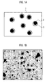
Figs. 1A and 1B are a schematic diagram and an SEM photograph, respectively, showing a structure of yttrium oxide in the case that the amount of SiO2 is larger than that of YF3 involved in a reaction; and -
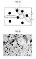
Figs. 2A and 2B are a schematic diagram and an SEM photograph, respectively, showing a structure of yttrium oxide in the case that the amount of SiO2 is less than that of YF3 involved in the reaction. - An yttrium oxide-containing material according to an embodiment of the present invention will be described below in detail, by comparison of strength, fracture toughness, and etching rate of the yttrium oxide-containing material between embodiment examples and comparative examples.
- In a first embodiment example, 96 vol.% yttrium oxide (Y2O3. prepared by Shin-Etsu Chemical, Co., Ltd., graded UUHP), 3 vol.% silicon carbide (SiC, prepared by Ibiden, Co., Ltd., Ultra-Fine), and 1 vol.% yttrium fluoride (YF3, prepared by Kojundo Chemical Lab., Co., Ltd.) were mixed together, and thereafter the resultant mixture was wet-blended for 24 hours using an IPA (isopropyl alcohol) solvent (a ball mill utilizing a ZrO2 pebbles is used) to obtain slurry. The obtained slurry was sieved and then dried for 16 hours in a 110°C nitrogen atmosphere, thereby obtaining powder. After the obtained dry powder was sieved, 80g of the powder was formed into a body of 50 mm in diameter under a pressure of 200 kg/cm2. At the end, hot press was applied to the formed body in a 1,600°C argon-gas atmosphere with a pressure of 200 kg/cm2, thereby obtaining an yttrium oxide-containing material in the first embodiment example.
- In a second embodiment example, the same process as in the first embodiment example was performed, but the proportions of Y2O3, SiC, and YF3 were 92 vol.%, 3 vol.%, and 5 vol.%, respectively, thereby obtaining an yttrium oxide-containing material in the second embodiment example.
- In a third embodiment example, the same process as in the first embodiment example was performed, but the proportions of Y2O3, SiC, and YF3 were 94 vol.%, 5 vol.%, and 1 vol.%, respectively, thereby obtaining an yttrium oxide-containing material in the third embodiment example.
- In a fourth embodiment example, the same process as in the first embodiment example was performed, but the proportions of Y2O3, SiC, and YF3 were 94 vol.%, 3 vol.%, and 3 vol.%, respectively, thereby obtaining an yttrium oxide-containing material in the fourth embodiment example.
- In a fifth embodiment example, the same process as in the first embodiment example was performed, but the proportions of Y2O3, SiC, and YF3 were 90 vol.%, 5 vol.%, and 5 vol.%, respectively, thereby obtaining an yttrium oxide-containing material in the fifth embodiment example.
- In a sixth embodiment example, the same process as in the first embodiment example was performed, but the proportions of Y2O3, SiC, and YF3 were 92 vol.%, 7 vol.%, and 1 vol.%, respectively, thereby obtaining an yttrium oxide-containing material in the sixth embodiment example.
- In a seventh embodiment example, the same process as in the first embodiment example was performed, but the proportions of Y2O3, SiC, and YF3 were 89 vol.%, 10 vol.%, and 1 vol.%, respectively, thereby obtaining an yttrium oxide-containing material in the seventh embodiment example.
- In an eighth embodiment example, the same process as in the first embodiment example was performed, but the proportions of Y2O3, SiC, and YF3 were 85 vol.%, 10 vol.%, and 5 vol.%, respectively, thereby obtaining an yttrium oxide-containing material in the eighth embodiment example.
- In a ninth embodiment example, the same process as in the first embodiment example was performed, but the proportions of Y2O3, SiC, and YF3 were 86 vol.%, 13 vol.%, and 1 vol.%, respectively, thereby obtaining an yttrium oxide-containing material in the ninth embodiment example.
- In a tenth embodiment example, the same process as in the first embodiment example was performed, but the proportions of Y2O3, SiC, and YF3 were 82 vol.%, 13 vol.%, and 5 vol.%, respectively, thereby obtaining an yttrium oxide-containing material in the tenth embodiment example.
- In a first comparative example, a sintered body was formed only using yttrium oxide (Y2O3, prepared by Shin-Etsu Chemical, Co., Ltd., graded UUHP).
- In a second comparative example, the same process as in the first embodiment example was performed, but the proportions of Y2O3 and YF3 were 95 vol.% and 5 vol.%, respectively, thereby obtaining an yttrium oxide-containing material in the second comparative example.
- In a third comparative example, the same process as in the first embodiment example was performed, but the proportions of Y2O3, SiC, and YF3 were 85 vol.%, 5 vol.%, and 10 vol.%, respectively, thereby obtaining an yttrium oxide-containing material in the third comparative example.
- In a fourth comparative example, the same process as in the first embodiment example was performed, but the proportions of Y2O3, SiC, and YF3 were 80 vol.%, 5 vol.%, and 15 vol.%, respectively, thereby obtaining an yttrium oxide-containing material in the fourth comparative example.
- In a fifth comparative example, the same process as in the first embodiment example was performed, but the proportions of Y2O3 and SiC were 80 vol.% and 20 vol.%, respectively, thereby obtaining an yttrium oxide-containing material in the fifth comparative example.
- By using an x-ray diffractometer (rotating-target x-ray diffractometer (RINT of Rigaku Corporation), CuKα radiation, 50 kV, 300 mA, 2θ = 10° to 70°), crystalline phases were identified based on x-ray diffraction patterns obtained from each yttrium oxide-containing material of the first to the tenth embodiment examples and of the first to the fifth comparative examples. As a result, as shown in the following table 1, the yttrium oxide-containing materials in the first, the third, the sixth, the seventh, and the ninth embodiment examples and in the fifth comparative example were found to be composed of yttrium oxide, (Y2O3), silicon carbide (SiC), and Y2SiO5, and the yttrium oxide-containing materials in the second, the fifth, the eighth, and the tenth embodiment examples and in the third and the fourth comparative examples were found to be composed of Y2O3, SiC, and YOF. Furthermore, the yttrium oxide-containing material in the fourth embodiment example was found to be composed of Y2O3 and SiC.
Table. 1 PREPARED COMPOSITION (Vol%) CRYSTALLINE PHASE SiC AVERAGE GRAIN SIZE (µm) YOF AVERAGE GRAIN SIZE (µm) STRENGTH (MPa) FRACTURE TOUGHNESS (MPa√m) ETCHING RATE (nm I h) Y2O3 SiC YF3 EMBODIMENT EXAMPLE 1 96 3 1 Y203,SiC,Y2SiO5 1.2 - 260 1.3 249 EMBODIMENT EXAMPLE 2 92 3 5 Y203,SiC,YOF 0.9 2 250 1.5 252 EMBODIMENT EXAMPLE 3 94 5 1 Y203,SiC,Y2SiO5 1.3 - 280 1.4 256 EMBODIMENT EXAMPLE 4 94 3 3 Y203,SiC 1.2 - 300 1.5 259 EMBODIMENT EXAMPLE 5 90 5 5 Y203,SiC,YOF 1.2 3 270 1.6 258 EMBODIMENT EXAMPLE 6 92 7 1 Y2O3,SiC,Y2SiO5 1.5 - 320 1.5 272 EMBODIMENT EXAMPLE 7 89 10 1 Y2O3,SiC,Y2SiO5 1.6 - 340 1.6 289 EMBODIMENT EXAMPLE 8 85 10 5 Y203,SiC,YOF 1.3 5 320 1.9 269 EMBODIMENT EXAMPLE 9 86 13 1 Y203,SiC,Y2S105 1.6 - 330 2.1 296 EMBODIMENT EXAMPLE 10 82 13 5 Y2O3,SiC,YOF 1.3 4 300 2.2 271 COMPARATIVE EXAMPLE 1 100 0 0 Y2O3 - - 220 1.0 243 COMPARATIVE EXAMPLE 2 95 0 5 Y2O3YOF - 45 200 1.2 242 COMPARATIVE EXAMPLE 3 85 5 10 Y2O3,SiC,YOF 1.1 15 220 1.6 254 COMPARATIVE EXAMPLE 4 80 5 15 Y2O3,SiC,YOF 0.9 33 210 1.5 252 COMPARATIVE EXAMPLE 5 80 20 0 Y2O3,SiC,Y2SiO5 1.8 - 230 2.2 389 - Furthermore, the chemical structures of the yttrium oxide-containing materials in the first to the tenth embodiment examples were analyzed. As a result, it became clear that, when a small amount of YF3 was added (1 vol.% in the embodiment examples) and thus the amount of SiO2 was larger than that of YF3 involved in chemical reactions,
silicon carbide grains 2 included in Y2SiO5 materials 3 were dispersed in an yttrium-oxidebasal body 1 as shown inFigs. 1A and 1B , because reactions expressed by the followingchemical formulas
[Chemical Formula 1] 3SiO2 + 4YF3 → 3SiF4 ↑ + 2Y2O3
[Chemical Formula 2] SiO2 +Y2O3→ Y2SiO5
- In contrast, when a large amount of YF3 was added (5 vol.% in the embodiment examples) and the amount of SiO2 was smaller than that of YF3 involved in the chemical reactions, it became clear that the
silicon carbide grains 2 were dispersed in the yttrium-oxidebasal body 1 and an YOF region 4 was formed between thesilicon carbide particles 2 as shown inFigs. 2A and 2B , because the reaction expressed by theaforementioned chemical formula 1 and another reaction expressed by the followingchemical formula 3 proceeds.
[Chemical Formula 3] Y2O3 +YF3 → 3YOF
- Moreover, the average grain diameter of SiC in each yttrium oxide-containing material of the first to the tenth embodiment examples and of the third to the fifth comparative examples was examined by SEM photographs. As a result, the average grain diameter of SiC was found to be 3 µm or less. Furthermore, the average grain diameter of YOF in each yttrium oxide-containing material of the second, the fifth, the eighth, and the tenth embodiment examples and of the second to the fourth comparative examples was examined by SEM photographs. As a result, the average grain diameter of YOF of the second, the fifth, the eighth, and the tenth embodiment examples was found to be 10 µm or less.
- The yttrium oxide-containing materials in the first to the tenth embodiment examples and in the third to the fifth comparative examples were observed using backscattered electron images of an SEM for measurement of the average grain diameter of SiC in each yttrium oxide-containing material. As SiC grains smaller than 0.5 µm in diameter could not be measured accurately, a minor diameter of only grains of 0.5 µm or greater in diameter was measured, and an average value thereof was determined as an average grain diameter. As a result, the average grain diameter of SiC in any yttrium oxide-containing materials was found to be 2 µm or less. Also, comparatively large SiC grains, which are 0.5 µm or greater, existed mainly at a grain boundary. Although fine SiC grains of 0.5 µm or less could not be measured accurately, an SiC abundance ratio was found different depending on whether YF3 was added or not. Specifically, when YF3 was added, a number of fine SiC grains were observed within the yttrium oxide grains. In contrast, when YF3 was not added, fine SiC grains were hardly observed. The reason for this is not yet clear at present, but it is conceivable that the addition of YF3 enables low-temperature sintering and thereby fine SiC grains can stay stably, and also that the SiC grains are easily included in the yttrium oxide grains.
- For each yttrium oxide-containing material of the first to the tenth embodiment examples and of the first to the fifth comparative examples, three-point bending strength was measured by a three-point bending test The measurement result is shown in Table 1. As a result, the yttrium oxide-containing materials of the first to the tenth embodiment examples had three-point strength of 250 MPa or higher.
- For each yttrium oxide-containing material of the first to the tenth embodiment examples and of the first to the fifth comparative examples, fracture toughness was measured according to IF method (weight: 9.8N) in conformity to JlS_R_1607. The measurement result is shown in Table 1. As a result, the yttrium oxide-containing materials of the first to the tenth embodiment examples had fracture toughness of 1.3 MPa·m½ or higher. Furthermore, the materials containing YF3 had a tendency to have higher strength and fracture toughness even with a small amount of SiC. The reason for this is not yet clear at present time, but it is conceivable that the addition of YF3 leads to the fact that comparatively large SiC grains of 0.5 µm or greater exist at the grain boundary of yttrium oxide and that fine SiC grains smaller than 0.5 µm exist within the yttrium oxide grains, thereby resulting in effectively improved mechanical characteristics at the grain boundary and within the yttrium oxide grains.
- For each yttrium oxide-containing material of the first to the tenth embodiment examples and of the first to the fifth comparative examples, plasma-resistance test was performed using a corrosion resistance tester. Specifically, plasma was generated using gas containing NF3, O2, or Ar at 800W of ICP power, and the generated plasma was applied to a test piece at 300W bias power. Subsequently, an etching rate of each yttrium oxide-containing material was calculated by dividing a difference in level between a masked surface and an exposed surface by test duration. The calculation result is shown in Table 1. As a result, when the quantity, shape, dispersed state of the silicon carbide met certain conditions, the corrosion resistance of the yttrium oxide-containing material was not greatly deteriorated even when poor corrosion-resistant silicon carbide was added to excellent corrosion-resistant yttrium oxide.
- From the foregoing results, the yttrium oxide-containing materials in the embodiment examples were found to have high fracture toughness by the addition of silicon carbide, to have an improved sinterability by the addition of YF3, and to be strengthened because the low-temperature sintering became possible. Note that, as the amount of added YF3 is increased, the YOF grain diameter becomes larger and the strength is deteriorated accordingly. According to the yttrium oxide-containing materials in the embodiment examples, however, the YOF grain diameter is adjustable suitably.
- The room-temperature volume resistivity of each yttrium oxide-containing material in the first, the third, the sixth, the seventh, and the ninth embodiment examples and in the first comparative example was measured. The measurement of the volume resistivity was done in the atmosphere according to a method in conformity with JIS-C2141. The measurement of the relative permittivity was done by using a 4291A impedance analyzer after a surface of a plate-like sample 21 mm square and 0.1 mm in thickness had been polished to obtain a surface roughness of Ra = 0.1 µm or less. The measurement result is shown in the following Table 2.
TABLE 2 SiC ADDITIVE AMOUNT
(vol %)VOLUME RESISTIVITY AT ROOM TEMPERATURE
(Ω cm)RELATIVE PERMITTIVITY EMBODIMENT EXAMPLE 1 3 1016 OR ABOVE 16 EMBODIMENT EXAMPLE 3 5 1016 OR ABOVE 18.5 EMBODIMENT EXAMPLE 6 7 1016 OR ABOVE 18 EMBODIMENT EXAMPLE 7 10 1016 OR ABOVE 17.5 EMBODIMENT EXAMPLE 9 13 3 x 10¹³ NON-MEASURABLE COMPARATIVE EXAMPLE 1 0 1016 OR ABOVE 12 - As shown in Table 2, when the amount of added SiC was within the range of 0 to 10 vol.%, the room-temperature volume resistivity was 1016 Ω·cm or above, which means that the yttrium oxide-containing material maintains high resistivity. When the amount of added SiC was 13 vol.%, the room-temperature volume resistivity is 3 × 10¹³ Ω.cm, which means the yttrium oxide-containing material exhibits low resistivity. When no SiC was added, the relative permittivity of the yttrium oxide-containing material was 12, but when the amount of added SiC was within the range of 3 to 10 vol.%, the relative permittivity of the yttrium oxide-containing material was 16 to 18.5, which was comparatively high values. From the foregoing results, it became clear that the SiC addition within the range of 3 to 10 vol.% maintained high volume resistivity as well as increased the relative permittivity of the yttrium oxide-containing material.
- Note that Japanese Unexamined Patent Application Publication No.
2006-69843 
- F denotes an chucking force, ε denotes a relative permittivity, ε0 denotes an electric constant, V denotes an applied voltage, and d denotes a thickness of the dielectric (yttrium oxide-containing material).
- The reason why the conductivity is different between the present invention and the invention disclosed in Japanese Unexamined Patent Application Publication No.
2006-69843 2006-69843 2006-69843 - Although the present invention made by the present inventors has been described in reference to its embodiment, the statement and drawings constituting part of the disclosure of the present invention should not be regarded as limiting the present invention. For example, yttrium fluoride is contained in yttrium oxide in the foregoing embodiment, but rare-earth fluoride other than yttrium fluoride, such as Lanthanum Fluoride and Ytterbium Fluoride, is also available. As described, various alternative embodiments, examples, and operation techniques made by those skilled in the art on the basis of the foregoing embodiment are, of course, within the scope of the present invention.
Claims (15)
- An yttrium oxide-containing material comprising: at least,silicon (Si);carbon (C); andfluorine (F).
- The yttrium oxide-containing material according to claim 1, wherein a crystalline phase is composed of yttrium oxide (Y2O3) and silicon carbide (SiC).
- The yttrium oxide-containing material according to claim 1, wherein a crystalline phase is composed of yttrium oxide (Y2O3), silicon carbide (SiC), and at least one of a compound of SiO2 and Re2O3 (Re is a rare-earth element) and a compound of YF3 and Re2O3.
- The yttrium oxide-containing material according to claim 3, wherein the compound of SiO2 and Re2O3 is ReSiO5, and the compound of YF3 and Re2O3 is ReOF.
- The yttrium oxide-containing material according to claim 3 or 4, the rare-earth element is yttrium (Y).
- The yttrium oxide-containing material according to any one of claims 2 to 5, wherein a grain diameter of the silicon carbide is 3 µm or less.
- The yttrium oxide-containing material according to claim 5 or 6, wherein a grain diameter of the YOF is 10 µm or less.
- The yttrium oxide-containing material according to any one of claims 1 to 7, wherein three-point bending strength is 250 MPa or above.
- The yttrium-oxide containing material according to any one of claims 1 to 8, wherein fracture toughness is 1.3 MPa m½ or above.
- The yttrium oxide-containing material according to any one of claims 1 to 9, wherein porosity is 5% or below.
- The yttrium oxide-containing material according to any one of claims 1 to 10, wherein room-temperature volume resistivity is 1 × 10¹⁵ Ω-cm or above.
- The yttrium oxide-containing material according to any one of claims 1 to 11, wherein a relative permittivity is within a range of 16 to 20.
- A component of semiconductor manufacturing equipment, wherein at least a portion of the component is made of the yttrium oxide-containing material according to any one of claims 1 to 12.
- A method of producing the yttrium oxide-containing material according to any one of claims 1 to 12, comprising:a step of sintering mixed powder of yttrium oxide, silicon carbide, and rare-earth fluoride at a temperature between 1,300°C and 1,850°C.
- The method of producing the yttrium oxide-containing material according to claim 14, wherein the rare-earth fluoride is yttrium fluoride (YF3).
Applications Claiming Priority (2)
| Application Number | Priority Date | Filing Date | Title |
|---|---|---|---|
| JP2007062329 | 2007-03-12 | ||
| JP2008046329A JP5071856B2 (en) | 2007-03-12 | 2008-02-27 | Yttrium oxide material and member for semiconductor manufacturing equipment |
Publications (2)
| Publication Number | Publication Date |
|---|---|
| EP1972599A1 true EP1972599A1 (en) | 2008-09-24 |
| EP1972599B1 EP1972599B1 (en) | 2011-10-12 |
Family
ID=39521909
Family Applications (1)
| Application Number | Title | Priority Date | Filing Date |
|---|---|---|---|
| EP20080250811 Ceased EP1972599B1 (en) | 2007-03-12 | 2008-03-10 | Yttrium oxide-containing material, component of semiconductor manufacturing equipment, and method of producing yttrium oxide-containing material |
Country Status (2)
| Country | Link |
|---|---|
| US (1) | US7833924B2 (en) |
| EP (1) | EP1972599B1 (en) |
Cited By (1)
| Publication number | Priority date | Publication date | Assignee | Title |
|---|---|---|---|---|
| EP2090557A3 (en) * | 2008-02-13 | 2012-02-01 | NGK Insulators, Ltd. | Yttrium oxide material, member for use in semiconductor manufacturing apparatus, and method for producing yttrium oxide material |
Families Citing this family (9)
| Publication number | Priority date | Publication date | Assignee | Title |
|---|---|---|---|---|
| EP1992430A1 (en) * | 2007-05-15 | 2008-11-19 | Treibacher Industrie AG | Yttria-based refractory composition |
| JP5117891B2 (en) * | 2008-03-11 | 2013-01-16 | 日本碍子株式会社 | Yttrium oxide material, member for semiconductor manufacturing apparatus, and method for manufacturing yttrium oxide material |
| US9440886B2 (en) | 2013-11-12 | 2016-09-13 | Applied Materials, Inc. | Rare-earth oxide based monolithic chamber material |
| JP5911036B1 (en) * | 2014-11-21 | 2016-04-27 | 日本イットリウム株式会社 | Sintered body |
| US9957192B2 (en) | 2016-03-29 | 2018-05-01 | Applied Materials, Inc. | Low temperature fluoride glasses and glazes |
| US11572617B2 (en) | 2016-05-03 | 2023-02-07 | Applied Materials, Inc. | Protective metal oxy-fluoride coatings |
| US12074050B2 (en) * | 2017-03-30 | 2024-08-27 | Sumitomo Osaka Cement Co., Ltd. | Composite sintered body, electrostatic chuck member, electrostatic chuck device, and method for producing composite sintered body |
| US10443125B2 (en) | 2017-05-10 | 2019-10-15 | Applied Materials, Inc. | Flourination process to create sacrificial oxy-flouride layer |
| KR102266656B1 (en) * | 2020-12-10 | 2021-06-18 | (주)코미코 | Yittrium granular powder for thermal spray and thermal spray coating produced using the same |
Citations (13)
| Publication number | Priority date | Publication date | Assignee | Title |
|---|---|---|---|---|
| JPH01219062A (en) * | 1988-02-29 | 1989-09-01 | Toyota Motor Corp | Production of silicon nitride sintered body |
| EP0552635A1 (en) * | 1992-01-21 | 1993-07-28 | Sumitomo Electric Industries, Limited | Composite ceramics sintered body and method of manufacturing the same |
| JPH0733526A (en) * | 1993-07-20 | 1995-02-03 | Hitachi Ltd | High strength fluoride ceramics |
| JPH07315949A (en) * | 1994-05-23 | 1995-12-05 | Hitachi Ltd | Highly reliable heat resistant ceramics and turbine parts |
| EP1245696A2 (en) * | 2001-03-30 | 2002-10-02 | Toshiba Ceramics Co., Ltd. | Plasma resistant member |
| US20030029563A1 (en) * | 2001-08-10 | 2003-02-13 | Applied Materials, Inc. | Corrosion resistant coating for semiconductor processing chamber |
| US20050068519A1 (en) * | 2003-09-30 | 2005-03-31 | Tokyo Electron Limited | Method for monitoring status of system components |
| JP2006069843A (en) | 2004-09-02 | 2006-03-16 | Ibiden Co Ltd | Ceramic member for semiconductor manufacturing apparatus |
| DE102006000405A1 (en) * | 2005-08-19 | 2007-02-22 | Ngk Insulators, Ltd., Nagoya | Sintered yttria body, electrostatic chuck, and method of producing a sintered yttria body |
| US20070044716A1 (en) * | 2005-08-24 | 2007-03-01 | Tsutomu Tetsuka | Plasma processing apparatus |
| JP2007062329A (en) | 2005-09-02 | 2007-03-15 | Ngk Insulators Ltd | Manufacturing method of tire mold |
| JP2008046329A (en) | 2006-08-15 | 2008-02-28 | Nec Lcd Technologies Ltd | Liquid crystal display element and electronic device equipped with the same |
| JP7033286B2 (en) * | 2017-07-17 | 2022-03-10 | エービー ルドヴィグ スヴェンソン | Greenhouse screen |
Family Cites Families (8)
| Publication number | Priority date | Publication date | Assignee | Title |
|---|---|---|---|---|
| US5459111A (en) * | 1992-01-21 | 1995-10-17 | Sumitomo Electric Industries, Ltd. | Composite ceramics sintered body |
| JPH0733286A (en) | 1993-07-22 | 1995-02-03 | Konica Corp | Transfer deviation correction device for image forming apparatus |
| JP4231917B2 (en) | 1998-03-31 | 2009-03-04 | 独立行政法人物質・材料研究機構 | Method for producing yttrium oxide fired body |
| JP2001179080A (en) | 1999-12-27 | 2001-07-03 | Nihon Ceratec Co Ltd | Substrate processing materials with low metal contamination |
| US7371704B2 (en) * | 2002-12-25 | 2008-05-13 | Ngk Insulators, Ltd. | Sintered bodies of yttrium-aluminum garnet, a method of producing the same and sintering aid therefor |
| DE112004001391B4 (en) * | 2003-07-29 | 2014-07-17 | Kyocera Corp. | Corrosion resistant component and method for producing the same and a component for a semiconductor or liquid crystal generating equipment |
| JP4648030B2 (en) * | 2005-02-15 | 2011-03-09 | 日本碍子株式会社 | Yttria sintered body, ceramic member, and method for producing yttria sintered body |
| JP5363132B2 (en) * | 2008-02-13 | 2013-12-11 | 日本碍子株式会社 | Yttrium oxide material, member for semiconductor manufacturing apparatus, and method for manufacturing yttrium oxide material |
-
2008
- 2008-03-07 US US12/043,988 patent/US7833924B2/en active Active
- 2008-03-10 EP EP20080250811 patent/EP1972599B1/en not_active Ceased
Patent Citations (13)
| Publication number | Priority date | Publication date | Assignee | Title |
|---|---|---|---|---|
| JPH01219062A (en) * | 1988-02-29 | 1989-09-01 | Toyota Motor Corp | Production of silicon nitride sintered body |
| EP0552635A1 (en) * | 1992-01-21 | 1993-07-28 | Sumitomo Electric Industries, Limited | Composite ceramics sintered body and method of manufacturing the same |
| JPH0733526A (en) * | 1993-07-20 | 1995-02-03 | Hitachi Ltd | High strength fluoride ceramics |
| JPH07315949A (en) * | 1994-05-23 | 1995-12-05 | Hitachi Ltd | Highly reliable heat resistant ceramics and turbine parts |
| EP1245696A2 (en) * | 2001-03-30 | 2002-10-02 | Toshiba Ceramics Co., Ltd. | Plasma resistant member |
| US20030029563A1 (en) * | 2001-08-10 | 2003-02-13 | Applied Materials, Inc. | Corrosion resistant coating for semiconductor processing chamber |
| US20050068519A1 (en) * | 2003-09-30 | 2005-03-31 | Tokyo Electron Limited | Method for monitoring status of system components |
| JP2006069843A (en) | 2004-09-02 | 2006-03-16 | Ibiden Co Ltd | Ceramic member for semiconductor manufacturing apparatus |
| DE102006000405A1 (en) * | 2005-08-19 | 2007-02-22 | Ngk Insulators, Ltd., Nagoya | Sintered yttria body, electrostatic chuck, and method of producing a sintered yttria body |
| US20070044716A1 (en) * | 2005-08-24 | 2007-03-01 | Tsutomu Tetsuka | Plasma processing apparatus |
| JP2007062329A (en) | 2005-09-02 | 2007-03-15 | Ngk Insulators Ltd | Manufacturing method of tire mold |
| JP2008046329A (en) | 2006-08-15 | 2008-02-28 | Nec Lcd Technologies Ltd | Liquid crystal display element and electronic device equipped with the same |
| JP7033286B2 (en) * | 2017-07-17 | 2022-03-10 | エービー ルドヴィグ スヴェンソン | Greenhouse screen |
Non-Patent Citations (1)
| Title |
|---|
| DATABASE WPI Week 198941, Derwent World Patents Index; AN 1989-296853, XP002485328 * |
Cited By (1)
| Publication number | Priority date | Publication date | Assignee | Title |
|---|---|---|---|---|
| EP2090557A3 (en) * | 2008-02-13 | 2012-02-01 | NGK Insulators, Ltd. | Yttrium oxide material, member for use in semiconductor manufacturing apparatus, and method for producing yttrium oxide material |
Also Published As
| Publication number | Publication date |
|---|---|
| EP1972599B1 (en) | 2011-10-12 |
| US20080226894A1 (en) | 2008-09-18 |
| US7833924B2 (en) | 2010-11-16 |
Similar Documents
| Publication | Publication Date | Title |
|---|---|---|
| EP1972599B1 (en) | Yttrium oxide-containing material, component of semiconductor manufacturing equipment, and method of producing yttrium oxide-containing material | |
| JP5071856B2 (en) | Yttrium oxide material and member for semiconductor manufacturing equipment | |
| EP3061739B1 (en) | Silicon nitride substrate and silicon nitride circuit board using same | |
| EP2090557B1 (en) | Yttrium oxide material, member for use in semiconductor manufacturing apparatus, and method for producing yttrium oxide material | |
| EP1988187A2 (en) | Apparatus and method which reduce the erosion rate of surfaces exposed to halogen-containing plasmas | |
| KR101400598B1 (en) | Corrosion-resistant member for a semiconductor manufacturing device, and manufacturing method therefor | |
| US8236722B2 (en) | Aluminum oxide sintered product and method for producing the same | |
| EP1245696A2 (en) | Plasma resistant member | |
| JP2020029614A (en) | Thermal spray coating, production method of thermal spray coating, thermal spray member and thermal spray material | |
| US7989380B2 (en) | High resistivity SiC material with B, N and O as the only additions | |
| EP1690845A1 (en) | Aluminum nitride joined article and method for manufacture thereof | |
| EP1314707B1 (en) | Aluminum nitride ceramics, members for use in a system for producing semiconductors, corrosion resistant members and conductive members | |
| US8231964B2 (en) | Aluminum oxide sintered body, method for producing the same and member for semiconductor producing apparatus | |
| KR100500495B1 (en) | Aluminium nitride ceramics, members for use in a system for producing semiconductors, and corrosion resistant members | |
| JP6015012B2 (en) | Electrostatic chuck member | |
| CN101665352A (en) | Alumina sintered body and method for producing same | |
| JP4889155B2 (en) | High-strength alumina sintered body having free machinability and corrosion-resistant member using the same | |
| KR100778274B1 (en) | Yttria sintered body and manufacturing method therefor | |
| JPH11335173A (en) | Aluminum nitride-base sintered compact and its production | |
| JP2009203113A (en) | Ceramics for plasma treatment apparatus | |
| KR100381589B1 (en) | Aluminum nitride sintered bodies and semiconductor-producing members including same | |
| KR20170014291A (en) | A SiC powder, SiC sintered body and Manufacturing method of the same |
Legal Events
| Date | Code | Title | Description |
|---|---|---|---|
| PUAI | Public reference made under article 153(3) epc to a published international application that has entered the european phase |
Free format text: ORIGINAL CODE: 0009012 |
|
| AK | Designated contracting states |
Kind code of ref document: A1 Designated state(s): AT BE BG CH CY CZ DE DK EE ES FI FR GB GR HR HU IE IS IT LI LT LU LV MC MT NL NO PL PT RO SE SI SK TR |
|
| AX | Request for extension of the european patent |
Extension state: AL BA MK RS |
|
| 17P | Request for examination filed |
Effective date: 20090323 |
|
| 17Q | First examination report despatched |
Effective date: 20090420 |
|
| AKX | Designation fees paid |
Designated state(s): DE FR GB |
|
| GRAP | Despatch of communication of intention to grant a patent |
Free format text: ORIGINAL CODE: EPIDOSNIGR1 |
|
| GRAS | Grant fee paid |
Free format text: ORIGINAL CODE: EPIDOSNIGR3 |
|
| GRAA | (expected) grant |
Free format text: ORIGINAL CODE: 0009210 |
|
| AK | Designated contracting states |
Kind code of ref document: B1 Designated state(s): DE FR GB |
|
| REG | Reference to a national code |
Ref country code: GB Ref legal event code: FG4D |
|
| REG | Reference to a national code |
Ref country code: DE Ref legal event code: R096 Ref document number: 602008010367 Country of ref document: DE Effective date: 20111208 |
|
| PLBE | No opposition filed within time limit |
Free format text: ORIGINAL CODE: 0009261 |
|
| STAA | Information on the status of an ep patent application or granted ep patent |
Free format text: STATUS: NO OPPOSITION FILED WITHIN TIME LIMIT |
|
| 26N | No opposition filed |
Effective date: 20120713 |
|
| REG | Reference to a national code |
Ref country code: DE Ref legal event code: R097 Ref document number: 602008010367 Country of ref document: DE Effective date: 20120713 |
|
| REG | Reference to a national code |
Ref country code: FR Ref legal event code: PLFP Year of fee payment: 9 |
|
| REG | Reference to a national code |
Ref country code: FR Ref legal event code: PLFP Year of fee payment: 10 |
|
| REG | Reference to a national code |
Ref country code: FR Ref legal event code: PLFP Year of fee payment: 11 |
|
| PGFP | Annual fee paid to national office [announced via postgrant information from national office to epo] |
Ref country code: DE Payment date: 20240130 Year of fee payment: 17 Ref country code: GB Payment date: 20240201 Year of fee payment: 17 |
|
| PGFP | Annual fee paid to national office [announced via postgrant information from national office to epo] |
Ref country code: FR Payment date: 20240213 Year of fee payment: 17 |
|
| REG | Reference to a national code |
Ref country code: DE Ref legal event code: R119 Ref document number: 602008010367 Country of ref document: DE |
|
| GBPC | Gb: european patent ceased through non-payment of renewal fee |
Effective date: 20250310 |
|
| PG25 | Lapsed in a contracting state [announced via postgrant information from national office to epo] |
Ref country code: DE Free format text: LAPSE BECAUSE OF NON-PAYMENT OF DUE FEES Effective date: 20251001 |
|
| PG25 | Lapsed in a contracting state [announced via postgrant information from national office to epo] |
Ref country code: GB Free format text: LAPSE BECAUSE OF NON-PAYMENT OF DUE FEES Effective date: 20250310 |
|
| PG25 | Lapsed in a contracting state [announced via postgrant information from national office to epo] |
Ref country code: FR Free format text: LAPSE BECAUSE OF NON-PAYMENT OF DUE FEES Effective date: 20250331 |