EP1971017A2 - High voltage power supply - Google Patents
High voltage power supply Download PDFInfo
- Publication number
- EP1971017A2 EP1971017A2 EP07124034A EP07124034A EP1971017A2 EP 1971017 A2 EP1971017 A2 EP 1971017A2 EP 07124034 A EP07124034 A EP 07124034A EP 07124034 A EP07124034 A EP 07124034A EP 1971017 A2 EP1971017 A2 EP 1971017A2
- Authority
- EP
- European Patent Office
- Prior art keywords
- signal
- power
- high voltage
- output
- transistor
- Prior art date
- Legal status (The legal status is an assumption and is not a legal conclusion. Google has not performed a legal analysis and makes no representation as to the accuracy of the status listed.)
- Ceased
Links
Images



Classifications
-
- H—ELECTRICITY
- H02—GENERATION; CONVERSION OR DISTRIBUTION OF ELECTRIC POWER
- H02M—APPARATUS FOR CONVERSION BETWEEN AC AND AC, BETWEEN AC AND DC, OR BETWEEN DC AND DC, AND FOR USE WITH MAINS OR SIMILAR POWER SUPPLY SYSTEMS; CONVERSION OF DC OR AC INPUT POWER INTO SURGE OUTPUT POWER; CONTROL OR REGULATION THEREOF
- H02M1/00—Details of apparatus for conversion
- H02M1/36—Means for starting or stopping converters
-
- H—ELECTRICITY
- H02—GENERATION; CONVERSION OR DISTRIBUTION OF ELECTRIC POWER
- H02M—APPARATUS FOR CONVERSION BETWEEN AC AND AC, BETWEEN AC AND DC, OR BETWEEN DC AND DC, AND FOR USE WITH MAINS OR SIMILAR POWER SUPPLY SYSTEMS; CONVERSION OF DC OR AC INPUT POWER INTO SURGE OUTPUT POWER; CONTROL OR REGULATION THEREOF
- H02M7/00—Conversion of AC power input into DC power output; Conversion of DC power input into AC power output
- H02M7/42—Conversion of DC power input into AC power output without possibility of reversal
- H02M7/44—Conversion of DC power input into AC power output without possibility of reversal by static converters
- H02M7/48—Conversion of DC power input into AC power output without possibility of reversal by static converters using discharge tubes with control electrode or semiconductor devices with control electrode
-
- H—ELECTRICITY
- H02—GENERATION; CONVERSION OR DISTRIBUTION OF ELECTRIC POWER
- H02M—APPARATUS FOR CONVERSION BETWEEN AC AND AC, BETWEEN AC AND DC, OR BETWEEN DC AND DC, AND FOR USE WITH MAINS OR SIMILAR POWER SUPPLY SYSTEMS; CONVERSION OF DC OR AC INPUT POWER INTO SURGE OUTPUT POWER; CONTROL OR REGULATION THEREOF
- H02M1/00—Details of apparatus for conversion
- H02M1/32—Means for protecting converters other than automatic disconnection
-
- H—ELECTRICITY
- H02—GENERATION; CONVERSION OR DISTRIBUTION OF ELECTRIC POWER
- H02M—APPARATUS FOR CONVERSION BETWEEN AC AND AC, BETWEEN AC AND DC, OR BETWEEN DC AND DC, AND FOR USE WITH MAINS OR SIMILAR POWER SUPPLY SYSTEMS; CONVERSION OF DC OR AC INPUT POWER INTO SURGE OUTPUT POWER; CONTROL OR REGULATION THEREOF
- H02M1/00—Details of apparatus for conversion
- H02M1/0003—Details of control, feedback or regulation circuits
- H02M1/0038—Circuits or arrangements for suppressing, e.g. by masking incorrect turn-on or turn-off signals, e.g. due to current spikes in current mode control
-
- H—ELECTRICITY
- H02—GENERATION; CONVERSION OR DISTRIBUTION OF ELECTRIC POWER
- H02M—APPARATUS FOR CONVERSION BETWEEN AC AND AC, BETWEEN AC AND DC, OR BETWEEN DC AND DC, AND FOR USE WITH MAINS OR SIMILAR POWER SUPPLY SYSTEMS; CONVERSION OF DC OR AC INPUT POWER INTO SURGE OUTPUT POWER; CONTROL OR REGULATION THEREOF
- H02M3/00—Conversion of DC power input into DC power output
- H02M3/22—Conversion of DC power input into DC power output with intermediate conversion into AC
- H02M3/24—Conversion of DC power input into DC power output with intermediate conversion into AC by static converters
- H02M3/28—Conversion of DC power input into DC power output with intermediate conversion into AC by static converters using discharge tubes with control electrode or semiconductor devices with control electrode to produce the intermediate AC
- H02M3/325—Conversion of DC power input into DC power output with intermediate conversion into AC by static converters using discharge tubes with control electrode or semiconductor devices with control electrode to produce the intermediate AC using devices of a triode or a transistor type requiring continuous application of a control signal
- H02M3/335—Conversion of DC power input into DC power output with intermediate conversion into AC by static converters using discharge tubes with control electrode or semiconductor devices with control electrode to produce the intermediate AC using devices of a triode or a transistor type requiring continuous application of a control signal using semiconductor devices only
- H02M3/33507—Conversion of DC power input into DC power output with intermediate conversion into AC by static converters using discharge tubes with control electrode or semiconductor devices with control electrode to produce the intermediate AC using devices of a triode or a transistor type requiring continuous application of a control signal using semiconductor devices only with automatic control of the output voltage or current, e.g. flyback converters
Definitions
- the invention relates to a high voltage power supply (HVPS) for use in a laser printer or a laser replicator, and more particularly, to a HVPS to prevent abnormal operation, which can occur when power is initially supplied, and where a sudden overshoot phenomenon can occur in an output voltage.
- HVPS high voltage power supply
- a high voltage power supply is a device that receives input voltages (5V, 24V or the like) from a switching mode power supply (SMPS) and a main board and generates and outputs high voltages required for forming an image of a transcription process according to a pulse width modulation (PWM) signal of a controller.
- the HVPS transforms a DC input voltage of 24V into a high voltage in the range of several hundreds to several thousands of volts using a transformer, and outputs the voltage.
- FIG. 1 is a circuit view illustrating a conventional HVPS.
- a controller 10 outputs a power signal of 24V and a PWM signal.
- An input unit 20 converts the PWM signal provided from the controller 10 into a DC voltage using a RC low pass filter.
- a comparison unit 30 controls output of the power signal of 24V by comparing the DC voltage output signal of the RC low pass filter to a reference voltage signal.
- a transformation unit 40 converts the output signal of the comparison unit 30 into a transistor driving signal and transforms the converted driving signal into a high voltage type signal.
- a rectification unit 50 rectifies the high voltage type signal of the transformation unit 40 and finally outputs a high voltage signal of a DC type. The final output high voltage DC signal stabilizes the output of the rectification unit 50 using feedback to the comparison unit 30.
- the controller 10 provides the PWM signal using a logic control signal of 5V and the power signal of 24[V] when power is to be supplied to office automation (OA) devices by the HVPS.
- the PWM signal provided from the controller 10 does not maintain a logic HIGH state when the power signal of 24V is first input, the PWM signal is instantly detected as a LOW state and a high voltage peak is suddenly generated in a high voltage DC signal output.
- This phenomenon negatively influences each device in which a HVPS is used to supply power.
- this phenomenon negatively affects the lifetime of a high voltage roller and the formation of an image.
- the present general inventive concept provides a high voltage power supply that prevents a sudden overshoot phenomenon of a high output voltage, which can occur at the time when a PWM signal that transitions into a HIGH state is delayed with respect to the time when power is initially supplied.
- a high voltage power supply which includes a controller to provide a PWM (pulse width modulation) signal and a power signal, an input unit to receive the PWM signal provided from the controller, a comparison unit to control the power signal provided by the controller by comparing the received PWM signal filtered to a DC voltage level by the input unit to a reference voltage signal and to provide a controlled output power signal, a transformation unit to transform the controlled output power signal output from the comparison unit into a high voltage output signal, and a rectification unit to rectify the high voltage output signal output from the transformation unit into a high voltage DC signal, wherein the high voltage power supply further includes a power input delay unit to receive the power signal from the controller and to delay the output of the power signal to the comparison unit by a predetermined time from when the power signal is initially provided by the controller for input into the comparison unit.
- the controller may output a logic control signal, used to generate the PWM signal, to the power input delay unit and to control
- the power input delay unit may include: a first transistor becoming activated when the logic control signal is provided from the controller; and a second transistor becoming activated when the first transistor is activated, wherein the power signal supplied from the controller is input into the comparison unit by activating the second transistor.
- the first transistor may be an NPN transistor.
- a base of the first transistor may be connected to an output terminal of the controller which supplies the logic control signal, an emitter of the first transistor is grounded, and a collector of the first transistor is connected to a base of the second transistor.
- the second transistor may be a PNP transistor.
- a base of the second transistor may be connected to a collector of the first transistor, an emitter of the second transistor is connected to an output terminal of the controller which supplies the power signal, and a collector of the second transistor is connected to an input of the comparison unit.
- the high voltage power supply may be operated to cause the power signal to be input to the comparison unit a predetermined amount of time after the power signal is initially provided by the controller.
- the high voltage power supply is included in an image forming apparatus.
- the high voltage power supply wherein the power signal is output from the power input delay unit substantially immediately prior to the transition of the received PWM signal to a logic HIGH state.
- HVPS high voltage power supply
- the method may also include utilizing a logic control signal to provide the received PWM signal.
- the method of operating wherein the controlled output power signal may be outputted at a predetermined time after the power signal is initially received.
- the method of operating wherein the controlled output power signal is delayed until a time immediately prior to the transition of the received PWM signal to a logic HIGH state.
- a high voltage power supply which includes a controller to provide a PWM (pulse width modulation) signal and a power signal, an input unit to receive the PWM signal provided by the controller and to filter the PWM signal to a DC voltage level, a comparison unit to control the power signal provided by the controller by comparing the filtered PWM signal to a reference voltage signal and to output a controlled output power signal, a transformation unit to transform the controlled output power signal output from the comparison unit into a high voltage DC output signal, and a power input delay unit to receive the controller provided power signal and a logic control signal and to delay the output of the power signal to the comparison unit.
- PWM pulse width modulation
- the high voltage power supply wherein the power input delay unit includes a plurality of transistor devices configured to control the flow of the power signal provided by the controller unit to the comparison unit.
- the high voltage power supply wherein the transistor devices are connected in series.
- the high voltage power supply wherein at least one of the transistor devices is a NPN transistor and at least one other is a PNP transistor.
- a high voltage power supply which includes a power input delay unit to receive a power signal and a logic control signal and to delay the output of the received power signal, an input unit to receive a pulse width modulation (PWM) signal and to filter the PWM signal to a DC voltage level, a comparison unit to receive the delayed received power signal from the power input delay unit and to control the delayed received power signal by comparing the filtered PWM signal to a reference voltage signal and to output a controlled output power signal, a transformation unit to transform the controlled output power signal output from the comparison unit into a high voltage output signal, and a rectification unit to rectify the high voltage output signal output from the transformation unit into a high voltage DC level output.
- PWM pulse width modulation
- the high voltage power supply wherein the power input delay unit delays the output of the received power until immediately prior to a transition of the PWM signal to a logic HIGH state.
- a high voltage power output delay device which includes a power delay input unit to receive a power signal and to receive a logic control signal and to utilize the logic control signal to delay the output of a delayed power signal, a comparison unit to receive the delayed power signal to receive a filtered DC level pulse width modulation (PWM) signal and to control the delayed power signal by comparing the filtered PWM signal to a voltage reference signal, wherein the delayed power signal is output to the comparison unit immediately prior to the time the PWM signal transitions to a logic HIGH status, and wherein the delayed power signal is transformed into a high voltage signal to be output.
- PWM pulse width modulation
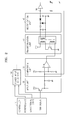
- FIG. 2 is a circuit view of a high voltage power supply (HVPS) according to an embodiment of the present general inventive concept.
- HVPS high voltage power supply
- a controller 10 provides a pulse width modulation (PWM) signal and power signal (e.g. 24V) that are generated by using a logic control signal (e.g. 5V).
- An input unit 20 receives the PWM signal provided from the controller 10, and converts the PWM signal into a DC voltage output signal using a RC low pass filter.
- a comparison unit 30 controls the output of the power signal (e.g. 24[V]) supplied from the controller 10 by comparing the DC voltage output signal output from the input unit 20 to a reference voltage signal.
- a transformation unit 40 transforms the controlled output power signal of the comparison unit 30 into a high voltage output signal.
- a rectification unit 50 rectifies the high voltage output signal of the transformation unit 40 and finally outputs a high voltage signal of DC type.
- the HVPS includes a power input delay unit 100 that delays the power signal (e.g. 24V) which is to be input into the comparison unit 30, by a predetermined amount of time, when the power signal (e.g. 24V) supplied from the controller 10 is input into the power input delay unit 100.
- a power input delay unit 100 that delays the power signal (e.g. 24V) which is to be input into the comparison unit 30, by a predetermined amount of time, when the power signal (e.g. 24V) supplied from the controller 10 is input into the power input delay unit 100.
- the controller 10 outputs the logic control signal (e.g. 5V) which is used to generate the PWM signal output from controller 10, as well as the power signal (e.g. 24V).
- the logic control signal e.g. 5V
- the power signal e.g. 24V
- Figure 3 is a circuit view illustrating the power input delay unit 100 illustrated in Figure 2 .
- the controller 10 outputs the power signal (e.g. 24V) into the power input delay unit 100 via a first terminal 12, and outputs the logic control signal (e.g. 5V) into the power input delay unit 100 via a second terminal 14. Meanwhile, the controller 10 generates the PWM signal using the logic control signal (e.g. 5V), and outputs the PWM signal to the input unit 20 via a third terminal 16.
- the power signal e.g. 24V
- the logic control signal e.g. 5V
- the controller 10 generates the PWM signal using the logic control signal (e.g. 5V), and outputs the PWM signal to the input unit 20 via a third terminal 16.
- the power input delay unit 100 of this embodiment includes a first transistor Tr1, a second transistor Tr2 and a plurality of resistors R1, R2, R3 and R4.
- the first transistor Tr1 is activated when the logic control signal (e.g. 5V) is provided from the controller 10.
- the first transistor Tr1 may be an NPN transistor, as illustrated in Figure 3 .
- the base of the first transistor Tr1 is connected to the second terminal 14 of the controller 10 which supplies the logic control signal (e.g. 5V).
- the resistor R1 is connected between the second terminal 14 and the base. The emitter of the first transistor Tr1 is grounded.
- resistor R2 is connected between the base and the emitter of the first transistor Tr1.
- the collector of the first transistor Tr1 is connected to the base of the second transistor Tr2.
- the resistor R3 is connected between the collector of the first transistor Tr1 and the base of the second transistor Tr2.
- the second transistor Tr2 is activated when the first transistor Tr1 is activated.
- the second transistor Tr2 may be a PNP transistor, as illustrated in Figure 3 .
- the base of the second transistor Tr2 is connected to the collector of the first transistor Tr1.
- the emitter of the second transistor Tr2 is connected to the first terminal 12 of the controller 10 which supplies the power signal (e.g. 24V).
- the resistor R4 is connected between the base and the emitter of the second transistor Tr2.
- the collector of the second transistor Tr2 is connected to the comparison unit 30, as illustrated in Figure 2 .
- the base of the first transistor Tr1 maintains a logic LOW state when the logic control signal (e.g. 5V) from controller 10 is not provided into the first transistor Tr1, which is an NPN transistor, the collector and the emitter of the first transistor Tr1 maintain an interrupted state.
- the base of the second transistor Tr2, which is a PNP transistor maintains a logic HIGH state when the collector and the emitter of the first transistor Tr1 maintains the interrupted state, the emitter and the collector of the second transistor Tr2 both maintain an interrupted state.
- the base of the first transistor Tr1 maintains the logic HIGH state when the logic control signal (e.g. 5V) is provided by controller 10 into the first transistor Tr1, the collector and the emitter of the first transistor Tr1 maintain the activated state. Furthermore, since the base of the second transistor Tr2 maintains the logic LOW state when the collector and the emitter of the first transistor Tr1 maintain the activated state, the emitter and the collector of the second transistor Tr2 also maintain the activated state.
- the power signal (e.g. 24V) supplied from the controller 10 is output into the comparison unit 30 by activation of the second transistor Tr2.
- Figures 4A and 4B illustrate a comparison of the signal that effect a HVPS according to an embodiment of the present invention ( Figure 4B ), with the signals that effect a conventional HVPS ( Figure 4A ).
- Figure 4A is a graph illustrating a change of an output voltage 3 output from an output terminal 18 of a conventional HVPS when power is supplied to the HVPS.
- a power signal 1 is supplied, where time T1 is substantially earlier than a time T2, where the PWM signal 2 transitions from a logic LOW state to a logic HIGH state, and thus sudden overshoot can be seen in the output voltage signal 3 output from the output terminal 18 of the HVPS.
- Figure 4B is a graph illustrating a change of an output voltage 3 output from the output terminal 18 of the HVPS according to the current embodiment when power is supplied to the HVPS.
- the power signal 1 of is supplied, which is delayed in time with respect to the time T1 when the power signal 1 of Figure 4A is supplied. This is because the power input delay unit 100 delays the power signal 1 of Figure 4B by a predetermined time after power signal 1 is initially supplied by controller 10 to be input into the comparison unit 30.
- time T3 when the power signal 1 is supplied is not substantially earlier than time T4 when the PWM signal 2 of Figure 4B transitions from the logic LOW state to the logic HIGH state, sudden overshoot of the output voltage signal 3 of the output terminal 18 of the HVPS does not occur, unlike in the conventional HVPS.
- the HVPS is operated at substantially the same time that the initial power is supplied. This is because overshoot of the output voltage signal 3 is likely to occur in the HVPS output terminal 18, as illustrated in Figure 4A , if the initial power is supplied substantially earlier than the transition of the PWM signal 2 of Figure 4B to a logic HIGH state.
- the HVPS may be included in an image forming apparatus.
- Components such as a roller or the like are likely to be damaged due to sudden overshoot of the output voltage signal in an image forming apparatus, in particular, in devices such as a printer and a replicator in which a high voltage is used.
- the HVPS according to the present general inventive concept is used in the image forming apparatus, and thus its components can be prevented from being damaged.
- the HVPS is a protective device for minimizing a negative affect on each roller circuit and other components of an image forming apparatus by controlling an output power signal when an input power signal is initially supplied.
- the HVPS can prevent components of a device from being damaged due to a sudden voltage surge in an output voltage of output terminal 18 of the device, which can occur at the time the PWM signal transitions to a logic HIGH state.
- the voltage surge is prevented by operation of the logic control signal causing the power signal 24V to be supplied to comparison unit 30, wherein it is delayed by the logic control signal until a time immediately prior to the time the PWM signal transitions to a logic HIGH state.
Landscapes
- Engineering & Computer Science (AREA)
- Power Engineering (AREA)
- Dc-Dc Converters (AREA)
Abstract
Description
- The invention relates to a high voltage power supply (HVPS) for use in a laser printer or a laser replicator, and more particularly, to a HVPS to prevent abnormal operation, which can occur when power is initially supplied, and where a sudden overshoot phenomenon can occur in an output voltage.
- A high voltage power supply (HVPS) is a device that receives input voltages (5V, 24V or the like) from a switching mode power supply (SMPS) and a main board and generates and outputs high voltages required for forming an image of a transcription process according to a pulse width modulation (PWM) signal of a controller. The HVPS transforms a DC input voltage of 24V into a high voltage in the range of several hundreds to several thousands of volts using a transformer, and outputs the voltage.
-
Figure 1 is a circuit view illustrating a conventional HVPS. Referring toFigure 1 , acontroller 10 outputs a power signal of 24V and a PWM signal. Aninput unit 20 converts the PWM signal provided from thecontroller 10 into a DC voltage using a RC low pass filter. Acomparison unit 30 controls output of the power signal of 24V by comparing the DC voltage output signal of the RC low pass filter to a reference voltage signal. Atransformation unit 40 converts the output signal of thecomparison unit 30 into a transistor driving signal and transforms the converted driving signal into a high voltage type signal. Arectification unit 50 rectifies the high voltage type signal of thetransformation unit 40 and finally outputs a high voltage signal of a DC type. The final output high voltage DC signal stabilizes the output of therectification unit 50 using feedback to thecomparison unit 30. - The
controller 10 provides the PWM signal using a logic control signal of 5V and the power signal of 24[V] when power is to be supplied to office automation (OA) devices by the HVPS. When the PWM signal provided from thecontroller 10 does not maintain a logic HIGH state when the power signal of 24V is first input, the PWM signal is instantly detected as a LOW state and a high voltage peak is suddenly generated in a high voltage DC signal output. This phenomenon negatively influences each device in which a HVPS is used to supply power. In particular, when a HVPS is used to supply power in an image forming apparatus, this phenomenon negatively affects the lifetime of a high voltage roller and the formation of an image. - The present general inventive concept provides a high voltage power supply that prevents a sudden overshoot phenomenon of a high output voltage, which can occur at the time when a PWM signal that transitions into a HIGH state is delayed with respect to the time when power is initially supplied.
- Additional aspects and utilities of the present general inventive concept will be set forth in part in the description which follows and, in part, will be obvious from the description, or may be learned by practice of the general inventive concept.
- The foregoing and/or other aspects and utilities of the present general inventive concept are achieved by providing a high voltage power supply which includes a controller to provide a PWM (pulse width modulation) signal and a power signal, an input unit to receive the PWM signal provided from the controller, a comparison unit to control the power signal provided by the controller by comparing the received PWM signal filtered to a DC voltage level by the input unit to a reference voltage signal and to provide a controlled output power signal, a transformation unit to transform the controlled output power signal output from the comparison unit into a high voltage output signal, and a rectification unit to rectify the high voltage output signal output from the transformation unit into a high voltage DC signal, wherein the high voltage power supply further includes a power input delay unit to receive the power signal from the controller and to delay the output of the power signal to the comparison unit by a predetermined time from when the power signal is initially provided by the controller for input into the comparison unit.
The controller may output a logic control signal, used to generate the PWM signal, to the power input delay unit and to control the delay of the power signal in the power input delay unit. - The power input delay unit may include: a first transistor becoming activated when the logic control signal is provided from the controller; and a second transistor becoming activated when the first transistor is activated, wherein the power signal supplied from the controller is input into the comparison unit by activating the second transistor.
- The first transistor may be an NPN transistor.
- A base of the first transistor may be connected to an output terminal of the controller which supplies the logic control signal, an emitter of the first transistor is grounded, and a collector of the first transistor is connected to a base of the second transistor.
- The second transistor may be a PNP transistor.
- A base of the second transistor may be connected to a collector of the first transistor, an emitter of the second transistor is connected to an output terminal of the controller which supplies the power signal, and a collector of the second transistor is connected to an input of the comparison unit.
- The high voltage power supply may be operated to cause the power signal to be input to the comparison unit a predetermined amount of time after the power signal is initially provided by the controller.
- The high voltage power supply is included in an image forming apparatus.
The high voltage power supply wherein the power signal is output from the power input delay unit substantially immediately prior to the transition of the received PWM signal to a logic HIGH state. - The foregoing and/or other aspects and utilities of the present general inventive concept are achieved by a method of operating a high voltage power supply (HVPS), including receiving a PWM signal and a power signal, controlling the received power signal by comparing the received PWM signal to a reference voltage signal and outputting a controlled output power signal, transforming the outputted controlled output power signal into a high voltage output signal, rectifying the high voltage output signal into a high voltage DC signal, and delaying the outputting of the controlled output power signal by a predetermined time after the power signal is initially received.
- The method may also include utilizing a logic control signal to provide the received PWM signal.
- The method of operating wherein the controlled output power signal may be outputted at a predetermined time after the power signal is initially received.
The method of operating wherein the controlled output power signal is delayed until a time immediately prior to the transition of the received PWM signal to a logic HIGH state. - The foregoing and/or other aspects and utilities of the present general inventive concept are achieved by a high voltage power supply which includes a controller to provide a PWM (pulse width modulation) signal and a power signal, an input unit to receive the PWM signal provided by the controller and to filter the PWM signal to a DC voltage level, a comparison unit to control the power signal provided by the controller by comparing the filtered PWM signal to a reference voltage signal and to output a controlled output power signal, a transformation unit to transform the controlled output power signal output from the comparison unit into a high voltage DC output signal, and a power input delay unit to receive the controller provided power signal and a logic control signal and to delay the output of the power signal to the comparison unit.
- The high voltage power supply wherein the power input delay unit includes a plurality of transistor devices configured to control the flow of the power signal provided by the controller unit to the comparison unit.
- The high voltage power supply wherein the transistor devices are connected in series.
- The high voltage power supply wherein at least one of the transistor devices is a NPN transistor and at least one other is a PNP transistor.
- The foregoing and/or other aspects and utilities of the present general inventive concept are achieved by a high voltage power supply which includes a power input delay unit to receive a power signal and a logic control signal and to delay the output of the received power signal, an input unit to receive a pulse width modulation (PWM) signal and to filter the PWM signal to a DC voltage level, a comparison unit to receive the delayed received power signal from the power input delay unit and to control the delayed received power signal by comparing the filtered PWM signal to a reference voltage signal and to output a controlled output power signal, a transformation unit to transform the controlled output power signal output from the comparison unit into a high voltage output signal, and a rectification unit to rectify the high voltage output signal output from the transformation unit into a high voltage DC level output.
- The high voltage power supply wherein the power input delay unit delays the output of the received power until immediately prior to a transition of the PWM signal to a logic HIGH state.
- The foregoing and/or other aspects and utilities of the present general inventive concept are achieved by a high voltage power output delay device which includes a power delay input unit to receive a power signal and to receive a logic control signal and to utilize the logic control signal to delay the output of a delayed power signal, a comparison unit to receive the delayed power signal to receive a filtered DC level pulse width modulation (PWM) signal and to control the delayed power signal by comparing the filtered PWM signal to a voltage reference signal, wherein the delayed power signal is output to the comparison unit immediately prior to the time the PWM signal transitions to a logic HIGH status, and wherein the delayed power signal is transformed into a high voltage signal to be output.
- Embodiments of the invention will now be described, by way of example, with reference to the accompanying drawings, in which:
-
Figure 1 is a circuit view illustrating a conventional high voltage power supply (HVPS); -
Figure 2 is a circuit view of a HVPS according to an embodiment of the present general inventive concept; -
Figure 3 is a circuit view illustrating an embodiment of the power input delay unit illustrated inFigure 2 ; and -
Figures 4A and 4B are, respectively, a graph of signals of a conventional HVPS, and a graph of signals of a HVPS according to an embodiment of the present general inventive concept. -
Figure 2 is a circuit view of a high voltage power supply (HVPS) according to an embodiment of the present general inventive concept. - Elements illustrated in
Figure 2 , which are respectively numbered the same as those illustrated inFigure 1 , are generally described in the background section herein, and now will be described in detail. Acontroller 10 provides a pulse width modulation (PWM) signal and power signal (e.g. 24V) that are generated by using a logic control signal (e.g. 5V). Aninput unit 20 receives the PWM signal provided from thecontroller 10, and converts the PWM signal into a DC voltage output signal using a RC low pass filter. Acomparison unit 30 controls the output of the power signal (e.g. 24[V]) supplied from thecontroller 10 by comparing the DC voltage output signal output from theinput unit 20 to a reference voltage signal. Atransformation unit 40 transforms the controlled output power signal of thecomparison unit 30 into a high voltage output signal. Arectification unit 50 rectifies the high voltage output signal of thetransformation unit 40 and finally outputs a high voltage signal of DC type. - According to embodiments of the present general inventive concept, the HVPS includes a power
input delay unit 100 that delays the power signal (e.g. 24V) which is to be input into thecomparison unit 30, by a predetermined amount of time, when the power signal (e.g. 24V) supplied from thecontroller 10 is input into the powerinput delay unit 100. - In this case, the
controller 10 outputs the logic control signal (e.g. 5V) which is used to generate the PWM signal output fromcontroller 10, as well as the power signal (e.g. 24V). -
Figure 3 is a circuit view illustrating the powerinput delay unit 100 illustrated inFigure 2 . - Referring to
Figure 3 , thecontroller 10 outputs the power signal (e.g. 24V) into the powerinput delay unit 100 via afirst terminal 12, and outputs the logic control signal (e.g. 5V) into the powerinput delay unit 100 via asecond terminal 14. Meanwhile, thecontroller 10 generates the PWM signal using the logic control signal (e.g. 5V), and outputs the PWM signal to theinput unit 20 via athird terminal 16. - The power
input delay unit 100 of this embodiment includes a first transistor Tr1, a second transistor Tr2 and a plurality of resistors R1, R2, R3 and R4. - The first transistor Tr1 is activated when the logic control signal (e.g. 5V) is provided from the
controller 10. In this case, the first transistor Tr1 may be an NPN transistor, as illustrated inFigure 3 . The base of the first transistor Tr1 is connected to thesecond terminal 14 of thecontroller 10 which supplies the logic control signal (e.g. 5V). The resistor R1 is connected between thesecond terminal 14 and the base. The emitter of the first transistor Tr1 is grounded. - Furthermore, the resistor R2 is connected between the base and the emitter of the first transistor Tr1. The collector of the first transistor Tr1 is connected to the base of the second transistor Tr2. The resistor R3 is connected between the collector of the first transistor Tr1 and the base of the second transistor Tr2.
- The second transistor Tr2 is activated when the first transistor Tr1 is activated. In this case, the second transistor Tr2 may be a PNP transistor, as illustrated in
Figure 3 . The base of the second transistor Tr2 is connected to the collector of the first transistor Tr1. The emitter of the second transistor Tr2 is connected to thefirst terminal 12 of thecontroller 10 which supplies the power signal (e.g. 24V). In addition, the resistor R4 is connected between the base and the emitter of the second transistor Tr2. The collector of the second transistor Tr2 is connected to thecomparison unit 30, as illustrated inFigure 2 . - Operations of the first transistor Tr1 and the second transistor Tr2, under the control of the logic control signal, will now be described. Since the base of the first transistor Tr1 maintains a logic LOW state when the logic control signal (e.g. 5V) from
controller 10 is not provided into the first transistor Tr1, which is an NPN transistor, the collector and the emitter of the first transistor Tr1 maintain an interrupted state. Since the base of the second transistor Tr2, which is a PNP transistor, maintains a logic HIGH state when the collector and the emitter of the first transistor Tr1 maintains the interrupted state, the emitter and the collector of the second transistor Tr2 both maintain an interrupted state. - However, since the base of the first transistor Tr1 maintains the logic HIGH state when the logic control signal (e.g. 5V) is provided by
controller 10 into the first transistor Tr1, the collector and the emitter of the first transistor Tr1 maintain the activated state. Furthermore, since the base of the second transistor Tr2 maintains the logic LOW state when the collector and the emitter of the first transistor Tr1 maintain the activated state, the emitter and the collector of the second transistor Tr2 also maintain the activated state. The power signal (e.g. 24V) supplied from thecontroller 10 is output into thecomparison unit 30 by activation of the second transistor Tr2. -
Figures 4A and 4B illustrate a comparison of the signal that effect a HVPS according to an embodiment of the present invention (Figure 4B ), with the signals that effect a conventional HVPS (Figure 4A ). -
Figure 4A is a graph illustrating a change of anoutput voltage ③ output from anoutput terminal 18 of a conventional HVPS when power is supplied to the HVPS. Referring toFigure 4A , at time T1, apower signal ① is supplied, where time T1 is substantially earlier than a time T2, where thePWM signal ② transitions from a logic LOW state to a logic HIGH state, and thus sudden overshoot can be seen in theoutput voltage signal ③ output from theoutput terminal 18 of the HVPS. -
Figure 4B is a graph illustrating a change of anoutput voltage ③ output from theoutput terminal 18 of the HVPS according to the current embodiment when power is supplied to the HVPS. Referring toFigure 4B , it can be seen that at a time T3, thepower signal ① of is supplied, which is delayed in time with respect to the time T1 when thepower signal ① ofFigure 4A is supplied. This is because the powerinput delay unit 100 delays thepower signal ① ofFigure 4B by a predetermined time afterpower signal ① is initially supplied bycontroller 10 to be input into thecomparison unit 30. Since the time T3, when thepower signal ① is supplied, is not substantially earlier than time T4 when thePWM signal ② ofFigure 4B transitions from the logic LOW state to the logic HIGH state, sudden overshoot of theoutput voltage signal ③ of theoutput terminal 18 of the HVPS does not occur, unlike in the conventional HVPS. - According to the present invention, unlike the conventional HVPS operation of
Figure 4A , the HVPS is operated at substantially the same time that the initial power is supplied. This is because overshoot of theoutput voltage signal ③ is likely to occur in theHVPS output terminal 18, as illustrated inFigure 4A , if the initial power is supplied substantially earlier than the transition of thePWM signal ② ofFigure 4B to a logic HIGH state. - The HVPS may be included in an image forming apparatus.
- Components such as a roller or the like are likely to be damaged due to sudden overshoot of the output voltage signal in an image forming apparatus, in particular, in devices such as a printer and a replicator in which a high voltage is used.
- Accordingly, the HVPS according to the present general inventive concept is used in the image forming apparatus, and thus its components can be prevented from being damaged.
- The HVPS according to the present general inventive concept is a protective device for minimizing a negative affect on each roller circuit and other components of an image forming apparatus by controlling an output power signal when an input power signal is initially supplied. In addition, by using a simple architecture, the HVPS can prevent components of a device from being damaged due to a sudden voltage surge in an output voltage of
output terminal 18 of the device, which can occur at the time the PWM signal transitions to a logic HIGH state. The voltage surge is prevented by operation of the logic control signal causing thepower signal 24V to be supplied tocomparison unit 30, wherein it is delayed by the logic control signal until a time immediately prior to the time the PWM signal transitions to a logic HIGH state. - Although a few embodiments of the invention have been shown and described, it will be appreciated by those skilled in the art that changes may be made in these embodiments without departing from the principles of the general inventive concept, the scope of which is defined in the appended claims.
Claims (20)
- A high voltage power supply, comprising:signal providing means (10) for providing a control signal and a power signal;means (20, 30, 40, 50) for generating a high voltage output signal based on the power signal and the control signal; andmeans (100) for receiving the power signal from the signal providing means (10), and for providing the power signal to the generating means (20, 30, 40, 50) with a delay with respect to the time at which the power signal is received at the receiving means (100).
- A high voltage power supply according to claim 1, wherein the signal providing means comprises a controller and the control signal comprises a PWM (pulse width modulation) signal, the generating means further comprising:an input unit to receive the PWM signal provided from the controller;a comparison unit to control the power signal provided by the controller by comparing the received PWM signal filtered to a DC voltage level by the input unit to a reference voltage signal and to provide a controlled output power signal; anda transformation unit to transform the controlled output power signal, output from the comparison unit, into the high voltage output signal;wherein the high voltage power supply further comprises a rectification unit to rectify the high voltage output signal output from the transformation unit into a high voltage DC signal and the receiving means comprises a power input delay unit to receive the power signal from the controller and to delay the output of the power signal to the comparison unit by a predetermined time from when the power signal is initially provided by the controller for input into the comparison unit.
- A high voltage power supply according to claim 2, wherein the controller outputs a logic control signal used to generate the PWM signal to the power input delay unit to control the delay of the power signal in the power input delay unit.
- A high voltage power supply according to claim 3, wherein the power input delay unit includes a plurality of transistor devices configured to utilize the logic control signal to control the flow of the power signal from the controller to the comparison unit.
- A high voltage power supply according to claim 4, wherein the transistor devices are connected in series.
- A high voltage power supply according to claim 5, wherein at least one of the transistor devices is a NPN transistor and at least one other is a PNP transistor.
- A high voltage power supply according to any one of claims 3 to 6, wherein the power input delay unit comprises:a first transistor becoming activated when the logic control signal is provided from the controller; anda second transistor becoming activated when the first transistor is activated,wherein the power signal supplied from the controller is input into the comparison unit by activating the second transistor.
- A high voltage power supply according to claim 7, wherein the first transistor is an NPN transistor.
- A high voltage power supply according to claim 8, wherein a base of the first transistor is connected to an output terminal of the controller which supplies the logic control signal, an emitter of the first transistor is grounded, and a collector of the first transistor is connected to a base of the second transistor.
- A high voltage power supply according to of claim 7, 8 or 9, wherein the second transistor is a PNP transistor.
- A high voltage power supply according to claim 10, wherein a base of the second transistor is connected to a collector of the first transistor, an emitter of the second transistor is connected to an output terminal of the controller which supplies the power signal, and a collector of the second transistor is connected to an input of the comparison unit.
- A high voltage power supply according to any one of claims 2 to 11, wherein the high voltage power supply is operated to cause the power signal to be input to the comparison unit a predetermined amount of time after the power signal is initially provided by the controller.
- A high voltage power supply according to any one of clams 2 to 12, wherein the high voltage power supply is included in an image forming apparatus.
- A high voltage power supply according to any one of claims 2 to 13, wherein the power signal is output from the power input delay unit substantially immediately prior to the transition of the received PWM signal to a logic HIGH state.
- A method of providing a high voltage power supply, comprising:providing a control signal and a power signal using signal providing means (10);generating a high voltage output signal using generating means (20, 30, 40, 50), the high voltage output signal being based on the power signal and the control signal; andreceiving the power signal from the signal providing means (10), and providing the power signal to the generating means (20, 30, 40, 50) with a delay with respect to the time at which the power signal is received.
- A method according to claim 15, wherein the control signal comprises a PWM signal, the method further comprising:controlling the power signal received at the generating means by comparing the received PWM signal to a reference voltage signal and outputting a controlled output power signal;transforming the outputted controlled output power signal into the high voltage output signal;rectifying the high voltage output signal into a high voltage DC signal; anddelaying the outputting of the controlled output power signal by a predetermined time after the power signal is initially received.
- A method according to claim 16, further comprising utilizing a logic control signal to provide the received PWM signal.
- A method according to claim 17, wherein the controlled output power signal is outputted at a predetermined time after the power signal is initially received.
- A method according to claim 17 or 18, wherein the controlled output power signal is delayed until a time immediately prior to the transition of the received PWM signal to a logic HIGH state.
- A high voltage power output delay device, comprising:a power input delay unit to receive a power signal, to receive a logic control signal and to utilize the logic control signal to delay output of a delayed power signal;a comparison unit to receive the delayed power signal, to receive a filtered DC level pulse width modulation (PWM) signal, and to control the delayed power signal by comparing the filtered PWM signal to a voltage reference signal;wherein the delayed power signal is output to the comparison unit immediately prior to the time the PWM signal transitions to a logic HIGH state; and
wherein the delayed power signal is transformed into a high voltage signal to be output.
Applications Claiming Priority (1)
| Application Number | Priority Date | Filing Date | Title |
|---|---|---|---|
| KR20070026272 | 2007-03-16 |
Publications (2)
| Publication Number | Publication Date |
|---|---|
| EP1971017A2 true EP1971017A2 (en) | 2008-09-17 |
| EP1971017A3 EP1971017A3 (en) | 2016-10-26 |
Family
ID=39575458
Family Applications (1)
| Application Number | Title | Priority Date | Filing Date |
|---|---|---|---|
| EP07124034.5A Ceased EP1971017A3 (en) | 2007-03-16 | 2007-12-21 | High voltage power supply |
Country Status (4)
| Country | Link |
|---|---|
| US (1) | US7821798B2 (en) |
| EP (1) | EP1971017A3 (en) |
| KR (1) | KR101214168B1 (en) |
| CN (1) | CN101266423B (en) |
Families Citing this family (1)
| Publication number | Priority date | Publication date | Assignee | Title |
|---|---|---|---|---|
| KR20110106669A (en) * | 2010-03-23 | 2011-09-29 | 삼성전자주식회사 | High voltage power |
Family Cites Families (7)
| Publication number | Priority date | Publication date | Assignee | Title |
|---|---|---|---|---|
| JP2000224849A (en) * | 1999-01-25 | 2000-08-11 | Samsung Electro Mech Co Ltd | Flyback circuit for synchronous rectifier for zero- voltage switching |
| DE60112749D1 (en) * | 2000-04-24 | 2005-09-22 | Huawei Tech Co Ltd | DELAY ACTUATING PULSE WIDE ADJUSTMENT CIRCUIT FOR INTERMEDIATE FREQUENCY OR HIGH FREQUENCY |
| KR100491599B1 (en) * | 2002-08-29 | 2005-05-27 | 삼성전자주식회사 | high voltage generator |
| CN100370685C (en) * | 2002-08-30 | 2008-02-20 | 三垦电气株式会社 | Switching power supply unit |
| US7088078B2 (en) * | 2004-06-04 | 2006-08-08 | Astec International Limited | Soft-start circuit for power converters |
| US7170732B2 (en) * | 2004-08-10 | 2007-01-30 | Micrel Incorporated | Surge delay for current limiter |
| KR100574057B1 (en) * | 2004-11-04 | 2006-04-27 | 삼성전자주식회사 | High voltage power supply and high voltage power control method |
-
2007
- 2007-10-15 US US11/872,219 patent/US7821798B2/en active Active
- 2007-12-11 KR KR1020070128185A patent/KR101214168B1/en not_active Expired - Fee Related
- 2007-12-21 EP EP07124034.5A patent/EP1971017A3/en not_active Ceased
- 2007-12-29 CN CN2007103062601A patent/CN101266423B/en not_active Expired - Fee Related
Non-Patent Citations (1)
| Title |
|---|
| None * |
Also Published As
| Publication number | Publication date |
|---|---|
| CN101266423B (en) | 2012-05-02 |
| EP1971017A3 (en) | 2016-10-26 |
| US20080225557A1 (en) | 2008-09-18 |
| KR20080084554A (en) | 2008-09-19 |
| US7821798B2 (en) | 2010-10-26 |
| KR101214168B1 (en) | 2012-12-21 |
| CN101266423A (en) | 2008-09-17 |
Similar Documents
| Publication | Publication Date | Title |
|---|---|---|
| EP2290796B1 (en) | Switch mode power supply with burst mode | |
| US5625279A (en) | DC-DC converter with dynamically adjustable characteristics | |
| JP4498851B2 (en) | Power supply | |
| US6909621B2 (en) | System for and method of controlling standby power | |
| KR101422960B1 (en) | Power module and distributed power supplying apparatus having the same | |
| US7782034B2 (en) | Constant voltage power supply circuit and method of controlling the same | |
| US5936852A (en) | Switched mode power supply with both main output voltage and auxiliary output voltage feedback | |
| EP1971017A2 (en) | High voltage power supply | |
| JP4559201B2 (en) | Inrush current prevention circuit for DC / DC converter | |
| JP4423468B2 (en) | Power start circuit, start / stop order control device, and start / stop order control method | |
| JP4058767B2 (en) | Switching power supply | |
| KR100703181B1 (en) | Multi Output Voltage Power Supply | |
| JP2001016849A (en) | Switching converter device | |
| JP3661472B2 (en) | Power supply | |
| US20250183787A1 (en) | Power supply unit and adjustment method for over-power protection value thereof | |
| JP2005204443A (en) | Switching power supply circuit | |
| JPH11220871A (en) | Power supply | |
| KR100370057B1 (en) | Stand-by control circuit for power supplies switching | |
| KR100649192B1 (en) | Power supply of plasma display | |
| KR19980023748A (en) | Initial supply voltage stabilizer for monitor | |
| JP2007336744A (en) | Power circuit and power supply unit | |
| JP2005176409A (en) | DC power supply | |
| JPH1039591A (en) | Bias generator | |
| JP2006014409A (en) | Power supply | |
| JP2020167859A (en) | Correction circuit and power supply |
Legal Events
| Date | Code | Title | Description |
|---|---|---|---|
| PUAI | Public reference made under article 153(3) epc to a published international application that has entered the european phase |
Free format text: ORIGINAL CODE: 0009012 |
|
| AK | Designated contracting states |
Kind code of ref document: A2 Designated state(s): AT BE BG CH CY CZ DE DK EE ES FI FR GB GR HU IE IS IT LI LT LU LV MC MT NL PL PT RO SE SI SK TR |
|
| AX | Request for extension of the european patent |
Extension state: AL BA HR MK RS |
|
| RAP1 | Party data changed (applicant data changed or rights of an application transferred) |
Owner name: SAMSUNG ELECTRONICS CO., LTD. |
|
| PUAL | Search report despatched |
Free format text: ORIGINAL CODE: 0009013 |
|
| AK | Designated contracting states |
Kind code of ref document: A3 Designated state(s): AT BE BG CH CY CZ DE DK EE ES FI FR GB GR HU IE IS IT LI LT LU LV MC MT NL PL PT RO SE SI SK TR |
|
| AX | Request for extension of the european patent |
Extension state: AL BA HR MK RS |
|
| RIC1 | Information provided on ipc code assigned before grant |
Ipc: H02M 3/00 20060101AFI20160919BHEP Ipc: H02M 1/36 20070101ALI20160919BHEP Ipc: H02M 1/32 20070101ALI20160919BHEP Ipc: H02M 3/335 20060101ALI20160919BHEP |
|
| STAA | Information on the status of an ep patent application or granted ep patent |
Free format text: STATUS: REQUEST FOR EXAMINATION WAS MADE |
|
| 17P | Request for examination filed |
Effective date: 20170123 |
|
| RBV | Designated contracting states (corrected) |
Designated state(s): AT BE BG CH CY CZ DE DK EE ES FI FR GB GR HU IE IS IT LI LT LU LV MC MT NL PL PT RO SE SI SK TR |
|
| RAP1 | Party data changed (applicant data changed or rights of an application transferred) |
Owner name: S-PRINTING SOLUTION CO., LTD. |
|
| STAA | Information on the status of an ep patent application or granted ep patent |
Free format text: STATUS: EXAMINATION IS IN PROGRESS |
|
| 17Q | First examination report despatched |
Effective date: 20170324 |
|
| AKX | Designation fees paid |
Designated state(s): DE FR GB NL |
|
| AXX | Extension fees paid |
Extension state: AL Extension state: MK Extension state: BA Extension state: HR Extension state: RS |
|
| RAP1 | Party data changed (applicant data changed or rights of an application transferred) |
Owner name: HP PRINTING KOREA CO., LTD. |
|
| STAA | Information on the status of an ep patent application or granted ep patent |
Free format text: STATUS: THE APPLICATION HAS BEEN REFUSED |
|
| 18R | Application refused |
Effective date: 20181216 |