EP1971003A1 - Contact assembly, method for manufacturing same and electric connector - Google Patents
Contact assembly, method for manufacturing same and electric connector Download PDFInfo
- Publication number
- EP1971003A1 EP1971003A1 EP06822041A EP06822041A EP1971003A1 EP 1971003 A1 EP1971003 A1 EP 1971003A1 EP 06822041 A EP06822041 A EP 06822041A EP 06822041 A EP06822041 A EP 06822041A EP 1971003 A1 EP1971003 A1 EP 1971003A1
- Authority
- EP
- European Patent Office
- Prior art keywords
- contact
- parts
- contacts
- housing
- view
- Prior art date
- Legal status (The legal status is an assumption and is not a legal conclusion. Google has not performed a legal analysis and makes no representation as to the accuracy of the status listed.)
- Withdrawn
Links
- 238000004519 manufacturing process Methods 0.000 title claims abstract description 17
- 238000000034 method Methods 0.000 title claims abstract description 14
- 238000003825 pressing Methods 0.000 claims abstract description 18
- 238000005520 cutting process Methods 0.000 claims abstract description 8
- 230000013011 mating Effects 0.000 claims description 26
- 230000008878 coupling Effects 0.000 abstract 3
- 238000010168 coupling process Methods 0.000 abstract 3
- 238000005859 coupling reaction Methods 0.000 abstract 3
- 238000003466 welding Methods 0.000 description 37
- 238000000465 moulding Methods 0.000 description 16
- 239000011347 resin Substances 0.000 description 11
- 229920005989 resin Polymers 0.000 description 11
- 238000003780 insertion Methods 0.000 description 10
- 230000037431 insertion Effects 0.000 description 10
- 239000002184 metal Substances 0.000 description 5
- 230000004927 fusion Effects 0.000 description 2
- 238000005192 partition Methods 0.000 description 2
- 230000004075 alteration Effects 0.000 description 1
- 238000005452 bending Methods 0.000 description 1
- 239000004020 conductor Substances 0.000 description 1
- 230000001419 dependent effect Effects 0.000 description 1
- 230000006870 function Effects 0.000 description 1
- 238000012986 modification Methods 0.000 description 1
- 230000004048 modification Effects 0.000 description 1
Images








Classifications
-
- H—ELECTRICITY
- H01—ELECTRIC ELEMENTS
- H01R—ELECTRICALLY-CONDUCTIVE CONNECTIONS; STRUCTURAL ASSOCIATIONS OF A PLURALITY OF MUTUALLY-INSULATED ELECTRICAL CONNECTING ELEMENTS; COUPLING DEVICES; CURRENT COLLECTORS
- H01R43/00—Apparatus or processes specially adapted for manufacturing, assembling, maintaining, or repairing of line connectors or current collectors or for joining electric conductors
- H01R43/20—Apparatus or processes specially adapted for manufacturing, assembling, maintaining, or repairing of line connectors or current collectors or for joining electric conductors for assembling or disassembling contact members with insulating base, case or sleeve
-
- H—ELECTRICITY
- H01—ELECTRIC ELEMENTS
- H01R—ELECTRICALLY-CONDUCTIVE CONNECTIONS; STRUCTURAL ASSOCIATIONS OF A PLURALITY OF MUTUALLY-INSULATED ELECTRICAL CONNECTING ELEMENTS; COUPLING DEVICES; CURRENT COLLECTORS
- H01R31/00—Coupling parts supported only by co-operation with counterpart
- H01R31/06—Intermediate parts for linking two coupling parts, e.g. adapter
-
- H—ELECTRICITY
- H01—ELECTRIC ELEMENTS
- H01R—ELECTRICALLY-CONDUCTIVE CONNECTIONS; STRUCTURAL ASSOCIATIONS OF A PLURALITY OF MUTUALLY-INSULATED ELECTRICAL CONNECTING ELEMENTS; COUPLING DEVICES; CURRENT COLLECTORS
- H01R13/00—Details of coupling devices of the kinds covered by groups H01R12/70 or H01R24/00 - H01R33/00
- H01R13/40—Securing contact members in or to a base or case; Insulating of contact members
- H01R13/405—Securing in non-demountable manner, e.g. moulding, riveting
- H01R13/41—Securing in non-demountable manner, e.g. moulding, riveting by frictional grip in grommet, panel or base
-
- H—ELECTRICITY
- H01—ELECTRIC ELEMENTS
- H01R—ELECTRICALLY-CONDUCTIVE CONNECTIONS; STRUCTURAL ASSOCIATIONS OF A PLURALITY OF MUTUALLY-INSULATED ELECTRICAL CONNECTING ELEMENTS; COUPLING DEVICES; CURRENT COLLECTORS
- H01R43/00—Apparatus or processes specially adapted for manufacturing, assembling, maintaining, or repairing of line connectors or current collectors or for joining electric conductors
- H01R43/16—Apparatus or processes specially adapted for manufacturing, assembling, maintaining, or repairing of line connectors or current collectors or for joining electric conductors for manufacturing contact members, e.g. by punching and by bending
-
- Y—GENERAL TAGGING OF NEW TECHNOLOGICAL DEVELOPMENTS; GENERAL TAGGING OF CROSS-SECTIONAL TECHNOLOGIES SPANNING OVER SEVERAL SECTIONS OF THE IPC; TECHNICAL SUBJECTS COVERED BY FORMER USPC CROSS-REFERENCE ART COLLECTIONS [XRACs] AND DIGESTS
- Y10—TECHNICAL SUBJECTS COVERED BY FORMER USPC
- Y10T—TECHNICAL SUBJECTS COVERED BY FORMER US CLASSIFICATION
- Y10T29/00—Metal working
- Y10T29/49—Method of mechanical manufacture
- Y10T29/49002—Electrical device making
- Y10T29/49117—Conductor or circuit manufacturing
- Y10T29/49204—Contact or terminal manufacturing
- Y10T29/49208—Contact or terminal manufacturing by assembling plural parts
- Y10T29/49218—Contact or terminal manufacturing by assembling plural parts with deforming
Definitions
- the present invention relates to a contact assembly comprising an inner housing and a plurality of contacts, a method for manufacturing this contact assembly, and an electrical connector comprising this contact assembly.
- mini SD cards which are such that the external shape of SD memory cards is reduced have been used in electronic devices such as portable telephones, telephones, portable audios, PDAs (personal digital assistance), gaming devices, cameras, and information terminal devices.
- electronic devices such as portable telephones, telephones, portable audios, PDAs (personal digital assistance), gaming devices, cameras, and information terminal devices.
- mini SD cards because the external shape is small compared to SD cards, in order to connect a mini SD card to a socket for an SD card, a card adaptor is required which electrically connects the mini SD card and the socket for an SD card by holding the mini SD card while being connected to the socket for an SD card.
- FIGS. 21A through 23 has been known in the past as a card adaptor of this type for connecting a small card such as a mini SD card to a socket for a large card.
- FIGS. 21A and 21B show a conventional example of a card adaptor; FIG. 21A is a plan view, and FIG. 21B is a front view.
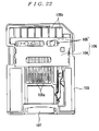
- FIG. 22 is a plan view of a state in which a contact assembly is fastened to a lower case.
- FIG. 23 is a plan view showing the contact assembly together with a card.
- the card adaptor 101 shown in FIGS. 21A through 23 is constructed from a contact assembly 106 comprising a plurality of contacts 105 and an inner housing 104 that holds the plurality of contacts 105 in parallel to each other, and an upper case 102 and a lower case 103 that accommodate this contact assembly 106. Furthermore, the contact assembly 106 is formed by insert-molding. Moreover, as is shown in FIGS. 22 and 23 , each of the contacts 105 comprises an elastic contact part 105a that contacts one of the conductor pads of a small card C such as a mini SD card, and a terminal part 105b that is connected to a socket for a large card; such a contact 105 is formed by stamping and forming a metal plate. In addition, a card insertion slot 107 into which the small card C is inserted is formed in the front end portion (lower end portion in FIG. 21A ) of the card adaptor 101.
- a contact assembly 106 comprising the plurality of contacts 105 and the inner housing 104 is first formed by insert-molding as shown in FIG. 23 .
- this contact assembly 106 is placed on the lower case 103 and fastened in place as shown in FIG. 22 .
- the upper case 102 is placed over the lower case 103 as shown in FIG. 21A , and a plurality of fusion parts 102a provided on the upper case 102 are fusion-bonded by ultrasonic welding or the like. As a result, a card adaptor 101 is completed.
- the contact pressure against the elastic contact parts 105a by means of the conductive pads provided on the small card C is dependent upon the gap for the insertion of the small card C between the elastic contact parts 105a and the upper surface of the lower case 103 that faces these elastic contact parts 105a; if this gap is large, the contact pressure is small, and if the gap is small, the contact pressure is large. Accordingly, it is necessary to control this gap at an appropriate value.
- the lower case 103 that faces the elastic contact parts 105a cannot be manufactured simultaneously, so that it is difficult to control the gap between the elastic contact parts 105a and the upper surface of the lower case 103 at an appropriate value. Therefore, variance tends to be generated in the contact pressure against the elastic contact parts 105a by means of the conductive pads provided on the small card C, so that there is a danger that the electrical connection between the small card C and the card adaptor 101 cannot be established properly.
- FIGS. 24 and 25 have also been known as another example of a card adaptor for connecting a small card such as a mini SD card to a socket for a large card.
- FIG. 24 is an exploded perspective view of another conventional example of a card adaptor.
- FIG 25 is a perspective view showing a contact member together with a lower case.
- the card adaptor 201 shown in FIG. 24 is constructed from a plurality of contacts 206, a lower case 203 which accommodates the plurality of contacts 206 in the interior and in which these contacts 206 are press-fitted, an upper case 202 that is fastened to the lower case 203, and a write protection tab 204.
- each of the contacts 206 comprises a securing part 206a that is press-fitted into a press-fitting groove 203a in the lower case 203, an elastic contact part 206b that is positioned in a recessed groove 203b in the lower case 203 and that contacts a conductive pad of a small card (not shown in the figures), and a terminal part 206c that is positioned inside a through-hole 203c in the lower case 203 and that is connected to a socket for a large card.
- a card insertion slot 205 into which a small card is inserted is formed in the front end portion (left end portion in FIG. 24 ) of the card adaptor 201.
- a contact member 210 is first manufactured by stamping and forming a metal plate, with this contact member 210 being formed by connecting adjacent contacts 206 to each other by means of linking pieces 209 and connecting the linking pieces 209 and a carrier 207 by means of connecting pieces 208.
- the securing parts 206a of the plurality of contacts 206 are respectively press-fitted into the press-fitting grooves 203a in the lower case 203 from above, the elastic contact parts 206b of the contacts 206 are respectively positioned in the recessed grooves 203b in the lower case 203, and the terminal parts 206c of the contacts 206 are respectively positioned inside the through-holes 203c in the lower case 203.
- the linking pieces 209 are cut to separate the adjacent contacts 206 from each other, and the connecting pieces 208 are cut to separate the carrier 207 from the linking pieces 209.
- the upper case 202 is placed over the lower case 203, and a plurality of fusion parts (not shown in the figures) provided on the upper case 202 are fusion-bonded to the lower case 203 by ultrasonic welding or the like.
- a card adaptor 201 is completed.
- a small card is inserted from the card insertion slot 205 in the front end portion of the card adaptor 101 toward the rear, and the conductive pads formed on the undersurface of the small card respectively make contact with the elastic contact parts 206b of the individual contacts 206 from above, and press these elastic contact parts 206b downward.
- the securing parts 206a of the plurality of contacts 206 are respectively press-fitted into the press-fitting grooves 203a in the lower case 203 from above, and the press-fitting direction of these securing parts 206a is the same as the direction of pressing against the elastic contact parts 206b of the respective contacts 206 by means of the conductive pads of the small card.
- the variance in the press-fitting positions of the securing parts 206a in the press-fitting direction causes variance to be generated easily in the pressing force against the elastic contact parts 206b of the respective contacts 206 by means of the conductive pads of the small card, i.e., in the contact pressure, so that even with the card adaptor 201 shown in FIGS. 24 and 25 , the electrical connection between the small card and card adaptor 201 is still not established properly in some instances.
- the present invention was devised in light of these problems; it is an object of the present invention to provide a contact assembly in which variance tends not to be generated in the pressing force against the elastic contact parts of the contacts by means of the mating contact parts such as the conductive pads of a small card, i.e., in the contact pressure, a method for manufacturing this contact assembly, and an electrical connector comprising this contact assembly.
- the contact assembly of Claim 1 is a contact assembly comprising a plurality of contacts having elastic contact parts that respectively contact mating contact parts, and an inner housing that holds the plurality of contacts, wherein the plurality of contacts are secured to the inner housing by press-fitting a contact member (that is formed as an integral unit by linking the plurality of contacts to each other by means of linking parts) in the inner housing in a direction perpendicular to the direction of pressing against the elastic contact parts by means of the mating contact parts, and the respective contacts are separated by cutting the linking parts between the respective contacts.
- a contact member that is formed as an integral unit by linking the plurality of contacts to each other by means of linking parts
- the electrical connector of Claim 2 comprises the contact assembly according to Claim 1 and an outer housing that accommodates this contact assembly.
- the method for manufacturing a contact assembly of Claim 3 comprises a step of press-fitting a contact member (which is formed as an integral unit by linking a plurality of contacts to each other by means of linking parts and in which the respective contacts have elastic contact parts that contact mating contact parts) in an inner housing in a direction perpendicular to the direction of pressing against the elastic contact parts by means of the mating contact parts, and a step of cutting the linking parts between the respective contacts of the press-fitted contact member.
- the plurality of contacts are secured to the inner housing by press-fitting a contact member (that is formed as an integral unit by linking the plurality of contacts to each other by means of linking parts) in the inner housing in a direction perpendicular to the direction of pressing against the elastic contact parts by means of the mating contact parts. Therefore, even if the press-fitting positions of the respective contacts vary in the press-fitting direction, variance is not likely to be generated in the pressing force against the elastic contact parts of the respective contacts by means of the mating contact parts, i.e., in the contact pressure. Accordingly, it is possible to provide a contact assembly that can establish electrical connection properly between the mating contact parts and the respective contacts. Furthermore, because the contact assembly is not formed by insert-molding, the mold is simple, and the manufacturing cost can be lowered. Moreover, because insert-molding is not required, there is no problem of difficulty in the resin selection.
- the plurality of contacts are secured to the inner housing by press-fitting in this inner housing a contact member that is formed as an integral unit by linking the plurality of contacts to each other by means of linking parts, and the respective contacts are separated by cutting the linking parts between the respective contacts. Therefore, the manufacturing process can be simplified compared to a case in which the individual contacts are press-fitted separately in the inner housing.
- the electrical connector of Claim 2 comprises the contact assembly according to Claim 1 and an outer housing that accommodates this contact assembly, it is possible to provide an electrical connector comprising a contact assembly that does not cause variance to be generated easily in the pressing force against the elastic contact parts of the respective contacts by means of the mating contact parts, i.e., in the contact pressure.
- the method for manufacturing a contact assembly of Claim 3 includes a step of press-fitting a contact member (which is formed as an integral unit by linking a plurality of contacts to each other by means of linking parts and in which the respective contacts have elastic contact parts that contact mating contact parts) in an inner housing in a direction perpendicular to the direction of pressing against the elastic contact parts by means of the mating contact parts. Therefore, even if the press-fitting positions of the respective contacts vary in the press-fitting direction, a contact assembly can be manufactured in which variance is not likely to be generated in the pressing force against the elastic contact parts of the respective contacts by means of the mating contact parts, i.e., in the contact pressure.
- this method includes a step of press-fitting in this inner housing a contact member which is formed as an integral unit by linking a plurality of contacts to each other by means of linking parts and in which the respective contacts have elastic contact parts that contact mating contact parts, and a step of cutting the linking parts between the respective contacts of the press-fitted contact member. Accordingly, the manufacturing process can be simplified compared to a case in which the individual contacts are press-fitted separately in the inner housing.
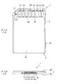
- FIGS. 1A and 1B show an electrical connector comprising the contact assembly of the present invention
- FIG. 1A is a plan view
- FIG. 1B is a front view
- FIGS. 2A and 2B show the electrical connector of FIGS. 1A and 1B
- FIG. 2A is a left side view
- FIG. 2B is an underside view
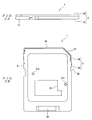
- FIGS. 3A and 3B show the contact assembly
- FIG. 3A is a plan view
- FIG. 3B is a front view
- FIGS. 4A and 4B show the contact assembly of FIGS. 3A and 3B
- FIG. 4A is a left side view
- FIG. 4B is a sectional view along line 4B-4B in FIG. 3A .
- the electrical connector 1 shown in FIGS. 1A, 1B , 2A and 2B is used as a card adaptor for connecting a small card such as a mini SD card (not shown in the figures) to a socket for a large card (not shown in the figures), and comprises the contact assembly 2 shown in FIGS. 3A, 3B , 4A and 4B and an outer housing 3 that accommodates this contact assembly 2 and that consists of a base housing 30 and a cover housing 40.
- the contact assembly 2 comprises a plurality of contacts 21 1 through 21 8 (eight contacts in the present embodiment), an inner housing 10 that fastens these contacts 21 1 through 21 8 in parallel to each other, and a hook spring 127.
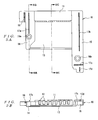
- FIGS. 5A and 5B show the inner housing;
- FIG. 5A is a plan view, and
- FIG. 5B is a front view.
- FIGS. 6A, 6B, 6C and 6D show the inner housing;
- FIG. 6A is a left side view
- FIG. 6B is a sectional view along line 6B-6B in FIG. 5A
- FIG. 6C is a sectional view along line 6C-6C in FIG. 5A
- FIG. 6D is a rear view.
- FIG. 7 is an underside view of the inner housing of FIG. 5A .
- the inner housing 10 is formed in a substantially rectangular shape by molding an insulating resin, and comprises a contact securing part 11 that extends in the direction of width (left-right direction in FIG. 5A ) as shown in FIGS. 3A through 6D .
- a plurality of contact press-fitting holes 12 for the press-fitting parts 22 (see FIG. 8A ) of the plurality of contacts 21 1 through 21 8 to be press-fitted are formed in a single row in this contact securing part 11.
- the respective contact press-fitting holes 12 are formed near the upper surface of the contact fastening part 11, and extend in the forward-rearward direction of the contact securing part 11 (in the vertical direction in FIG. 5A ).
- a left side wall 14 that extends in the forward direction is provided on the left end portion in the direction of width of the contact securing part 11, and a right side wall 15 that protrudes in the forward direction more than the left side wall 14 is provided on the right end portion in the direction of width of the contact securing part 11.
- a bottom wall 13 that extends in the forward direction up to the front end of the left side wall 14 and that covers the bottom surface of the inner housing 10 is provided on the bottom surface of the contact securing part 11.
- a first post through-hole 16a that passes through in the vertical direction and a hook spring press-fitting hole 18 that extends in the forward-rearward direction and that is used for the press-fitting of the hook spring 127 are formed in the left side wall 14 of the inner housing 10.
- a welding part 17a that extends in the forward-rearward direction is formed in a protruding manner on the upper surface of this left side wall 14.
- a second post through-hole 16b that passes through in the vertical direction is formed in the right side wall 15 of the inner housing 10.
- a welding part 17b that extends in the forward-rearward direction, a welding part 17c that extends in the left-right direction, and a welding part 17d that extends in the forward-rearward direction are formed in a protruding manner on the upper surface of this right side wall 15.
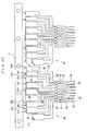
- FIGS. 8A and 8B show a contact member in which a plurality of contacts are connected to each other by linking parts and formed as an integral unit;
- FIG. 8A is a plan view
- FIG. 8B is a front view.
- FIGS. 9A and 9B show the contact member of FIGS. 8A and 8B ;
- FIG. 9A is a left side view
- FIG. 9B is a rear view.
- FIG. 10 is a plan view of a state in which a plurality of contact members are linked to a carrier.
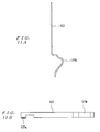
- FIGS. 11A and 11B show the hook spring;
- FIG. 11A is a plan view
- FIG. 11B is a left side view.
- each of the plurality of contacts 21 1 through 21 8 comprises a press-fitting part 22 that is press-fitted in the contact securing part 11 of the inner housing 10, an elastic contact part 23 that extends forward from the front end of the press-fitting part 22, a linking part 24 that extends from the rear end of the press-fitting part 22, and a terminal part 25 that is provided at the rear end of the linking part 24.
- a separate terminal part 25a is connected via a short-circuit part 25b to the terminal part 25 of the sixth contact 21 6 from the left (seventh terminal part from the left including this separate terminal part 25a).
- each elastic contact part 23 has a contact part that extends forward from the front end of the press-fitting part 22 and is then curved into a downward convex shape, so that one of the conductive pads (mating contact parts) provided on the upper surface of a small card such as a mini SD card contacts this contact part.
- the conductive pads respectively make contact with the contact parts of the individual elastic contact parts 23, the conductive pads push the contact parts upward, so that the contact parts are displaced upward with the press-fitting parts 22 as fixed ends.
- the terminal parts provided on a socket for a large card with which the electrical connector 1 mates respectively contact the individual terminal parts 25 and the separate terminal part 25a.
- the hook spring 127 is formed by stamping and forming a metal plate, and is provided with a curved locking part 127b at the front end and a press-fitting part 127a at the rear end as shown in FIGS. 11A and 11B .
- the press-fitting part 127a is press-fitted, rearward from the front, into the hook spring press-fitting hole 18 formed in the inner housing 10.
- the curved locking part 127b is formed by bending so as to form an inward convex shape, and is locked with a cutout (not shown in the figures) that is formed in one side edge of the small card inserted into the electrical connector 1, thus possessing the function of holding the small card.
- a method for manufacturing the contact assembly 2 will be described with reference to FIGS. 3A, 3B , 8A, 8B and 10 .
- a plurality of contact members 20 that are linked to a carrier C are prepared as shown in FIG. 10 .
- This state is formed by stamping and forming a metal plate.
- the linking piece 24 of the first contact 21 1 from the left and the linking piece 24 of the second contact 21 2 from the left are linked by a linking part 26a
- the terminal part 25 of the first contact 21 1 from the left and the linking piece 24 of the second contact 21 2 from the left are linked by a linking part 26b.
- linking piece 24 of the second contact 21 2 from the left and the linking piece 24 of the third contact 21 3 from the left are linked by a linking part 26c.
- linking piece 24 of the third contact 21 3 from the left and the separate terminal part 25a are linked by a linking part 26d, and the terminal part 25 of the third contact 21 3 from the left and the separate terminal part 25a are linked by a linking part 26e.
- the linking piece 24 of the third contact 21 3 from the left and the linking piece 24 of the fourth contact 21 4 from the left are linked by a linking part 26f, and the separate terminal part 25a and the terminal part 25 of the fourth contact 21 4 from the left are linked by a linking part 26g.
- linking piece 24 of the fourth contact 21 4 from the left and the linking piece 24 of the fifth contact 21 5 from the left are linked by a linking part 26h
- the terminal part 25 of the fourth contact 21 4 from the left and the terminal part 25 of the fifth contact 21 5 from the left are linked by a linking part 26i
- the linking piece 24 of the fifth contact 21 5 from the left and the linking piece 24 of the sixth contact 21 6 from the left are linked by a linking part 26j
- the terminal part 25 of the fifth contact 21 5 from the left and the terminal part 25 of the sixth contact 21 6 from the left are linked by a linking part 26k.
- each contact member 20 is formed as an integral unit, with the plurality of contacts 21 1 through 21 8 (eight contacts in the present embodiment) being linked to each other by the linking parts 26a through 26n.
- each contact member 20 is formed in the shape of a lead frame formed by stamping and forming a metal plate. Then, each contact member 20 is linked to the carrier C by a connecting piece 27a that connects the terminal part 25 of the second contact 21 2 from the left and the carrier C, a connecting piece 27b that connects the terminal part 25 of the third contact 21 3 from the left and the carrier C, a connecting piece 27c that connects the terminal part 25 of the seventh contact 21 7 from the left and the carrier C, and a connecting piece 27d that connects the terminal part 25 of the eighth contact 21 8 from the left and the carrier C.
- a connecting piece 27a that connects the terminal part 25 of the second contact 21 2 from the left and the carrier C
- a connecting piece 27b that connects the terminal part 25 of the third contact 21 3 from the left and the carrier C
- a connecting piece 27c that connects the terminal part 25 of the seventh contact 21 7 from the left and the carrier C
- a connecting piece 27d that connects the terminal part 25 of the eighth contact 21 8
- one of the contact members 20 that are linked to the carrier C is press-fitted in the inner housing 10 in a direction perpendicular to the direction of pressing against the elastic contact parts 23 by means of the conductive pads (mating contact parts) provided on the upper surface of the small card, i.e., in the forward direction from the rear of the inner housing 10.
- the press-fitting parts 22 of the respective contacts 21 1 through 21 8 are press-fitted into the contact press-fitting holes 12 in the inner housing 10.
- the contact member 20 is press-fitted in the inner housing 10 in a direction perpendicular to the direction of pressing against the elastic contact parts 23 by means of the mating contact parts, even if the press-fitting positions of the respective contacts 21 1 through 21 8 vary in the press-fitting direction (i.e., in the forward-rearward direction), variance is not likely to be generated in the pressing force against the elastic contact parts 23 of the respective contacts 21 1 through 21 8 by means of the mating contact parts, i.e., in the contact pressure. Accordingly, it is possible to provide a contact assembly 2 which can achieve the proper electrical connection between the mating contact parts and the respective contacts 21 1 through 21 8 .
- the contact member 20 is press-fitted in the inner housing 10 in a direction perpendicular to the direction of pressing against the elastic contact parts 23 by means of the mating contact parts as in the present embodiment, no variance is generated in the strength for holding the respective contacts 21 1 through 21 8 , and this holding strength can also be enhanced.
- the connecting pieces 27a through 27d are cut to separate the carrier C from the contact member 20, and in the contact member 20, the linking parts 26a through 26n between the individual contacts 21 1 through 21 8 are also cut to separate the respective contacts 21 1 through 21 8 .
- the plurality of contacts 21 1 through 21 8 (eight contacts in the present embodiment) are attached to the inner housing 10 as shown in FIGS. 3A and 3B .
- the plurality of contacts 21 1 through 21 8 are formed as an integral unit by being linked to each other by the linking parts 26a through 26n, and the present embodiment includes a step of press-fitting, in the inner housing 10, the contact member 20 in which the respective contacts 21 1 through 21 8 have the elastic contact parts 23 that contact the mating contact parts, and a step of cutting the linking parts 26a through 26n between the individual contacts 21 1 through 21 8 of the press-fitted contact member 20. Accordingly, the manufacturing process can be simplified compared to a case in which the individual contacts 21 1 through 21 8 are press-fitted separately in the inner housing 10.
- the contact assembly 2 is completed. Furthermore, because insert-molding is not necessary in the manufacture of the contact assembly 2, the mold is simple, and the manufacturing cost can be reduced. Moreover, because insert-molding is not necessary, there is no problem of difficulty in the selection of the resin for forming the inner housing 10.
- FIGS. 12A and 12B show the base housing; FIG. 12A is a plan view, and FIG. 12B is a front view.
- FIGS.13A, 13B and 13C show the base housing of FIGS. 12A and 12B ;
- FIG. 13A is a left side view,
- FIG. 13B is a right side view, and
- FIG. 13C is a rear view.
- FIGS. 14A, 14B and 14C show the base housing of FIGS. 12A and 12B ;
- FIG. 14A is a sectional view along line 14A-14A in FIG. 12A
- FIG. 14B is a sectional view along line 14B-14B in FIG. 12A
- FIG. 14C is a sectional view along line 14C-14C in FIG. 12A .
- FIG. 15 is an underside view of the base housing of FIGS. 12A and 12B .
- the base housing 30 that partly makes up the outer housing 3 is formed in a substantially rectangular shape by molding an insulating resin, and an inner housing accommodating space 31 for accommodating the inner housing 10 is formed substantially in the central portion as shown in FIG. 12A .
- a through-hole 32 with which the platform part 13 of the inner housing 10 mates is formed in the bottom wall of this inner housing accommodating space 31.
- a card insertion slot 33 that opens on the front side is formed to the front of the inner housing accommodating space 31, and the upper portions of the inner housing accommodating space 31 and card insertion slot 33 are open.
- a carrying stand part 34 on which the linking pieces 24 and terminal parts 25 of the plurality of contacts 21 1 through 21 8 secured to the inner housing 10 are carried is provided to the rear side of the inner housing accommodating space 31.
- a plurality of partition walls 35 1 through 35 8 that divide between adjacent terminal parts of the terminal parts 25 of the respective contacts 21 1 through 21 8 and the separate terminal part 25a are provided in the area near the rear end portion of this carrying stand part 34.
- a first post 36a that is fitted into the first post through-hole 16a in the inner housing 10 and a second post 36b that is fitted into the second post through-hole 16b are formed in a protruding manner on the bottom wall of the inner housing accommodating space of the base housing 30.
- a third post through-hole 37a and a fourth post through-hole 37b are respectively formed in the left and right side wall parts of the base housing 30.
- two welding parts 38a and 38b that extend in the forward-rearward direction and a welding part 38c that extends in the left-right direction are formed in a protruding manner on the upper surface of the front wall that is positioned to the left side of the card insertion slot 33 of the base housing 30.
- two welding parts 38d and 38e that extend in the forward-rearward direction are formed in a protruding manner on the upper surface of the left side wall of the base housing 30.
- a welding part 38f that extends in the left-right direction, a welding part 38g that extends in the forward-rearward direction, a welding part 38h that extends in a diagonal direction, four welding parts 38i, 38j, 38k, and 381 that extend in the left-right direction, and a welding part 38m that extends in the forward-rearward direction are formed in a protruding manner on the upper surface of the base housing 30 in the area around the carrying stand part 34.
- a welding part 38n that extends in the left-right direction and a welding part 38o that extends in the forward-rearward direction are formed in a protruding manner on the upper surface of the right side wall of the base housing 30.
- a welding part 38p that extends in the left-right direction and a welding part 38q that extends in the forward-rearward direction are formed in a protruding manner on the upper surface of the front wall that is positioned to the right side of the card insertion slot 33 of the base housing 30.
- three welding parts 38r, 38s, and 38t that extend in the left-right direction and two welding parts 38u and 38v that extend in the forward-rearward direction are formed in a protruding manner on the upper surface of the carrying stand part 34 of the base housing 30.
- an accommodating recessed part 39 for accommodating a write protection tab 4 is formed in the right side wall of the base housing 30.
- an engagement recessed part 50 with which a mating locking member engages when the electrical connector 1 mates with a socket for a large card is formed in the left side wall of the base housing 30.
- a tab accommodating part 39 for accommodating a write protection tab 4 is formed in the right side wall of the base housing 30.
- FIGS. 16A and 16B show the cover housing; FIG. 16A is a plan view, and FIG. 16B is a front view.
- FIGS. 17A, 17B and 17C show the cover housing of FIGS. 16A and 16B ;
- FIG. 17A is a left side view,
- FIG. 17B is a right side view, and
- FIG. 17C is a rear view.
- FIG. 18 is an underside view of the cover housing of FIG. 16A .
- FIGS. 19A, 19B, 19C and 19D show the cover housing of FIGS. 16A and 16B ;
- FIG. 19A is a sectional view along line 19A-19A in FIG. 18
- FIG. 19B is a sectional view along line 19B-19B in FIG. 18
- FIG. 19C is a sectional view along line 19C-19C in FIG. 18
- FIG. 19D is a sectional view along line 19D-19D in FIG. 18 .
- the cover housing 40 that partly makes up the outer housing 3 is formed in a rectangular shape that substantially overlaps with the base housing 30 by molding an insulating resin, and is designed to be superimposed on the base housing 30 and welded after the contact assembly 2 is placed on the base housing 30, and to accommodate the contact assembly 2 together with the base housing 30. As is shown in FIG. 18 , this cover housing 40 is provided, in substantially the central portion thereof, with a contact securing part recessed part 41 that covers the contact securing part 11 of the inner housing 10 accommodated in the base housing 30 when this cover housing 40 is welded to the base housing 30.
- a plurality of contact recessed parts 42 that respectively cover the elastic contact parts 23 of the plurality of contacts 21 1 through 21 8 accommodated in the base housing 30 when the cover housing 40 is welded to the base housing 30 are formed to the front side of the contact securing part recessed part 41.
- a push-in part 43 that pushes in the linking pieces 24 of the plurality of contacts 21 1 through 21 8 accommodated in the base housing 30 when the cover housing 40 is welded to the base housing 30 is provided to the rear side of the contact fastening part recessed part 41.
- a plurality of openings 44 for exposing the terminal parts 25 of the plurality of contacts 21 1 through 21 8 accommodated in the base housing 30 when the cover housing 40 is welded to the base housing 30 are formed to the rear side of this push-in part 43.
- a third post 45a that is fitted into the third post through-hole 37a in the base housing 30 and a fourth post 45b that is fitted into the fourth post through-hole 37b when the cover housing 40 is superimposed on the base housing 30 are formed on this cover housing 40 in a protruding manner.
- the cover housing 40 is provided with a plurality of welding part recessed parts 46a, 46b, 46c, 46d, 46e, 46n, 46o, 46p, 46q, 46r, 46s, 46t, 46u, 46v, 46w, and 46x where the apexes of the plurality of welding parts 38a, 38b, 38c, 38d, 38e, 38n, 38o, 38p, 38q, 38r, 38s, 38t, 38u, 38v, 38w, and 38x that are formed on the base housing 30 in a protruding manner respectively enter when the cover housing 40 is superimposed on the base housing 30.
- the cover housing 40 is also provided with a base seat part 47 which is contacted by the apexes of the welding parts 38f, 38g, 38h, 38i, 38j, 38k, 381, and 38m that are formed in a protruding manner on the upper surface of the base housing 30 in the area around the carrying stand part 34 when this cover housing 40 is superimposed on the base housing 30. Furthermore, a covering part 48 that covers the rear end edge of the base housing 30 when the cover housing 40 is welded to the base housing 30 is provided on the rear end edge of this base seat part 47. Moreover, an inclined surface 51 for preventing the reverse insertion is provided at the left corner portion of this covering part 48.
- cover housing 40 is provided with welding part recessed parts 49a, 49b, 49c, and 49d where the apexes of the welding parts 17a, 17b, 17c, and 17d formed in a protruding manner on the inner housing 10 respectively enter when this cover housing 40 is superimposed on the base housing 30.
- FIGS. 20A and 20B show a subassembly in which the contact assembly is mounted to the base housing; FIG. 20A is a plan view, and FIG. 20B is a sectional view along line 20B-20B in FIG. 20A .
- the contact assembly 2 shown in FIGS. 3A and 3B is manufactured using the method described above.
- the contact assembly 2 is placed on the base housing 30 as shown in FIGS. 20A and 20B .
- the inner housing 10 of the contact assembly 2 is accommodated in the inner housing accommodating space 31 in the base housing 30 while performing positioning by inserting the first post 36a of the base housing 30 into the first post through-hole 16a in the inner housing 10, and inserting the second post 36b into the second post through-hole 16b.
- the platform part 13 of the inner housing 10 is caused to mate with the through-hole 32 in the base housing 30, and the undersurface of the base housing 30 and the undersurface of the inner housing 10 become coplanar.
- the linking pieces 24 and terminal parts 25 of the respective contacts 21 1 through 21 8 and the separate terminal part 25a are placed on the carrying stand part 34 of the base housing 30.
- the spaces between adjacent terminal parts of the terminal parts and separate terminal part 25a are respectively divided by the plurality of partition walls 35 1 through 35 8 .
- the ultrasonic welding of the first post 36a and second post 36b of the base housing 30 is performed, thus fastening the inner housing 10 to the base housing 30.
- the cover housing 40 shown in FIGS. 16A through 19D is superimposed on the base housing 30.
- the third post 45a of the cover housing 40 is fitted into the third post through-hole 37a in the base housing 30
- the fourth post 45b is fitted into the fourth post through-hole 37b, thus positioning the cover housing 40 with respect to the base housing 30.
- the cover housing 40 when the cover housing 40 is superimposed on the base housing 30, the apexes of the plurality of welding parts 38a, 38b, 38c, 38d, 38e, 38n, 38o, 38p, 38q, 38r, 38s, 38t, 38u, 38v, 38w, and 38x that are formed on the base housing 30 in a protruding manner respectively enter the plurality of welding part recessed parts 46a, 46b, 46c, 46d, 46e, 46n, 46o, 46p, 46q, 46r, 46s, 46t, 46u, 46v, 46w, and 46x of the cover housing 40.
- the apexes of the welding parts 38f, 38g, 38h, 38i, 38j, 38k, 381, and 38m that are formed in a protruding manner on the upper surface of the base housing 30 in the area around the carrying stand part 34 contact the base seat part 47 of the cover housing 40.
- the apexes of the welding parts 17a, 17b, 17c, and 17d formed on the inner housing 10 in a protruding manner respectively enter the welding part recessed parts 49a, 49b, 49c, and 49d of the cover housing 40.
- the third post 45a and fourth post 45b of the cover housing 40, the welding parts 38a through 38x of the base housing 30, and the welding parts 17a through 17d of the inner housing 10 are ultrasonic welded, thus fastening the cover housing 40 to the base housing 30 and inner housing 10.
- the contact assembly 2 is accommodated in the outer housing 3 constructed from the base housing 30 and cover housing 40, and the electrical connector 1 shown in FIGS. 1A through 2B is completed.
- the contact securing part recessed part 41 of the cover housing 40 covers the contact securing part 11 of the inner housing 10.
- the plurality of contact recessed parts 42 of the cover housing 40 respectively cover the elastic contact parts 23 of the plurality of contacts 21 1 through 21 8 .
- the push-in part 43 of the cover housing 40 pushes in the linking pieces 24 of the plurality of contacts 21 1 through 21 8 , so that the terminal parts 25 provided at the rear ends of the linking pieces 24 are prevented from floating from the base housing 30.
- the terminal parts 25 of the plurality of contacts 21 1 through 21 8 and the separate terminal part 25a are exposed to the plurality of openings 44 in the cover housing 40 as shown in FIG. 1(A) , making it possible for the terminal parts provided on the socket for a large card with which the electrical connector 1 mates to contact these terminal parts 25 and separate terminal part 25a via the openings 44.
- the electrical connector 1 that has been assembled in this manner mates with the socket for a large card, and the terminal parts provided on this socket contact the terminal parts 25 of the plurality of contacts 21 1 through 21 8 and the separate terminal part 25a, thus establishing an electrical connection. Meanwhile, a small card is inserted into the card insertion slot 33 in the electrical connector 1, and the conductive pads (mating contact parts) provided on the upper surface of the small card respectively contact the elastic contact parts 23 of the individual contacts 21 1 through 21 8 . As a result, the small card is electrically connected to the socket for a large card via the respective contacts 21 1 through 21 8 .
- the contact assembly 2 may also be used in a device other than the electrical connector 1 used as a card adaptor for connecting a small card such as a mini SD card to a socket for a large card.
Landscapes
- Engineering & Computer Science (AREA)
- Manufacturing & Machinery (AREA)
- Coupling Device And Connection With Printed Circuit (AREA)
- Manufacturing Of Electrical Connectors (AREA)
- Connector Housings Or Holding Contact Members (AREA)
Abstract
A contact assembly in which variation in pressing force, or contact pressure of a contact against a resilient contact portion by the counterpart contact portion such as the conductive pad of a small card is suppressed. A method for manufacturing the contact assembly and an electric connector equipped with the contact assembly are also provided. In the contact assembly (2), a plurality of contacts (211-218) are secured to an inner housing (10) when a contact member (20) formed integrally by coupling the plurality of contacts (211-218) mutually through coupling portions (26a-26n) is press-fitted in the inner housing (10) in the direction intersecting the pressing direction to the resilient contact portion (23) by the counterpart contact portion perpendicularly and secured in place, and each of the contacts (211-218) is separated by cutting the coupling portion (26a-26n) between respective contacts (211-218).
Description
- The present invention relates to a contact assembly comprising an inner housing and a plurality of contacts, a method for manufacturing this contact assembly, and an electrical connector comprising this contact assembly.
- In recent years, mini SD cards which are such that the external shape of SD memory cards is reduced have been used in electronic devices such as portable telephones, telephones, portable audios, PDAs (personal digital assistance), gaming devices, cameras, and information terminal devices.
With such mini SD cards, because the external shape is small compared to SD cards, in order to connect a mini SD card to a socket for an SD card, a card adaptor is required which electrically connects the mini SD card and the socket for an SD card by holding the mini SD card while being connected to the socket for an SD card. - The card adaptor shown in
FIGS. 21A through 23 (seeJP2005-242448A FIGS. 21A and 21B show a conventional example of a card adaptor;FIG. 21A is a plan view, andFIG. 21B is a front view.FIG. 22 is a plan view of a state in which a contact assembly is fastened to a lower case.FIG. 23 is a plan view showing the contact assembly together with a card. - The
card adaptor 101 shown inFIGS. 21A through 23 is constructed from acontact assembly 106 comprising a plurality ofcontacts 105 and aninner housing 104 that holds the plurality ofcontacts 105 in parallel to each other, and anupper case 102 and alower case 103 that accommodate thiscontact assembly 106. Furthermore, thecontact assembly 106 is formed by insert-molding. Moreover, as is shown inFIGS. 22 and23 , each of thecontacts 105 comprises anelastic contact part 105a that contacts one of the conductor pads of a small card C such as a mini SD card, and aterminal part 105b that is connected to a socket for a large card; such acontact 105 is formed by stamping and forming a metal plate. In addition, acard insertion slot 107 into which the small card C is inserted is formed in the front end portion (lower end portion inFIG. 21A ) of thecard adaptor 101. - In the assembly of this
card adaptor 101, acontact assembly 106 comprising the plurality ofcontacts 105 and theinner housing 104 is first formed by insert-molding as shown inFIG. 23 . Next, thiscontact assembly 106 is placed on thelower case 103 and fastened in place as shown inFIG. 22 . Finally, theupper case 102 is placed over thelower case 103 as shown inFIG. 21A , and a plurality offusion parts 102a provided on theupper case 102 are fusion-bonded by ultrasonic welding or the like. As a result, acard adaptor 101 is completed. - In this
card adaptor 101, however, because thecontact assembly 106 is formed by insert-molding, a mold for performing this insert-molding is complicated, so that there is a problem in that the manufacturing cost becomes high. Furthermore, a resin for forming theinner housing 104 is required to perform insert-molding, but a resin with a large shrinkage rate cannot be selected in the molding, creating the problem of difficulty in the resin selection. - Moreover, the contact pressure against the
elastic contact parts 105a by means of the conductive pads provided on the small card C is dependent upon the gap for the insertion of the small card C between theelastic contact parts 105a and the upper surface of thelower case 103 that faces theseelastic contact parts 105a; if this gap is large, the contact pressure is small, and if the gap is small, the contact pressure is large. Accordingly, it is necessary to control this gap at an appropriate value. In the insert-molding, however, due to the restriction of the mold, thelower case 103 that faces theelastic contact parts 105a cannot be manufactured simultaneously, so that it is difficult to control the gap between theelastic contact parts 105a and the upper surface of thelower case 103 at an appropriate value. Therefore, variance tends to be generated in the contact pressure against theelastic contact parts 105a by means of the conductive pads provided on the small card C, so that there is a danger that the electrical connection between the small card C and thecard adaptor 101 cannot be established properly. - Meanwhile, the card adaptor shown in
FIGS. 24 and25 (seeJP2004-252672A FIG. 24 is an exploded perspective view of another conventional example of a card adaptor.FIG 25 is a perspective view showing a contact member together with a lower case. - The
card adaptor 201 shown inFIG. 24 is constructed from a plurality ofcontacts 206, alower case 203 which accommodates the plurality ofcontacts 206 in the interior and in which thesecontacts 206 are press-fitted, anupper case 202 that is fastened to thelower case 203, and awrite protection tab 204. Furthermore, each of thecontacts 206 comprises asecuring part 206a that is press-fitted into a press-fitting groove 203a in thelower case 203, anelastic contact part 206b that is positioned in arecessed groove 203b in thelower case 203 and that contacts a conductive pad of a small card (not shown in the figures), and aterminal part 206c that is positioned inside a through-hole 203c in thelower case 203 and that is connected to a socket for a large card. Moreover, acard insertion slot 205 into which a small card is inserted is formed in the front end portion (left end portion inFIG. 24 ) of thecard adaptor 201. - In the assembly of this
card adaptor 201, as is shown inFIG. 25 , acontact member 210 is first manufactured by stamping and forming a metal plate, with thiscontact member 210 being formed by connectingadjacent contacts 206 to each other by means of linkingpieces 209 and connecting the linkingpieces 209 and a carrier 207 by means of connectingpieces 208.
Next, thesecuring parts 206a of the plurality ofcontacts 206 are respectively press-fitted into the press-fitting grooves 203a in thelower case 203 from above, theelastic contact parts 206b of thecontacts 206 are respectively positioned in the recessedgrooves 203b in thelower case 203, and theterminal parts 206c of thecontacts 206 are respectively positioned inside the through-holes 203c in thelower case 203. Then, the linkingpieces 209 are cut to separate theadjacent contacts 206 from each other, and the connectingpieces 208 are cut to separate the carrier 207 from the linkingpieces 209. - Finally, the
upper case 202 is placed over thelower case 203, and a plurality of fusion parts (not shown in the figures) provided on theupper case 202 are fusion-bonded to thelower case 203 by ultrasonic welding or the like. As a result, acard adaptor 201 is completed.
Furthermore, a small card is inserted from thecard insertion slot 205 in the front end portion of thecard adaptor 101 toward the rear, and the conductive pads formed on the undersurface of the small card respectively make contact with theelastic contact parts 206b of theindividual contacts 206 from above, and press theseelastic contact parts 206b downward. - In this
card adaptor 201, because the plurality ofcontacts 206 are designed to be press-fitted in thelower case 203, there is no need for insert-molding, and the mold is simple, so that the manufacturing cost can be lowered. Moreover, because insert-molding is not required, there is no problem of difficulty in the resin selection. - However, the following problem has been encountered in the
card adaptor 201 shown inFIGS. 24 and25 :
Specifically, thesecuring parts 206a of the plurality ofcontacts 206 are respectively press-fitted into the press-fittinggrooves 203a in thelower case 203 from above, and the press-fitting direction of thesesecuring parts 206a is the same as the direction of pressing against theelastic contact parts 206b of therespective contacts 206 by means of the conductive pads of the small card. Therefore, the variance in the press-fitting positions of thesecuring parts 206a in the press-fitting direction causes variance to be generated easily in the pressing force against theelastic contact parts 206b of therespective contacts 206 by means of the conductive pads of the small card, i.e., in the contact pressure, so that even with thecard adaptor 201 shown inFIGS. 24 and25 , the electrical connection between the small card andcard adaptor 201 is still not established properly in some instances. - Accordingly, the present invention was devised in light of these problems; it is an object of the present invention to provide a contact assembly in which variance tends not to be generated in the pressing force against the elastic contact parts of the contacts by means of the mating contact parts such as the conductive pads of a small card, i.e., in the contact pressure, a method for manufacturing this contact assembly, and an electrical connector comprising this contact assembly.
- In order to solve the problems described above, the contact assembly of
Claim 1 is a contact assembly comprising a plurality of contacts having elastic contact parts that respectively contact mating contact parts, and an inner housing that holds the plurality of contacts, wherein the plurality of contacts are secured to the inner housing by press-fitting a contact member (that is formed as an integral unit by linking the plurality of contacts to each other by means of linking parts) in the inner housing in a direction perpendicular to the direction of pressing against the elastic contact parts by means of the mating contact parts, and the respective contacts are separated by cutting the linking parts between the respective contacts. - Furthermore, the electrical connector of
Claim 2 comprises the contact assembly according toClaim 1 and an outer housing that accommodates this contact assembly.
Moreover, the method for manufacturing a contact assembly ofClaim 3 comprises a step of press-fitting a contact member (which is formed as an integral unit by linking a plurality of contacts to each other by means of linking parts and in which the respective contacts have elastic contact parts that contact mating contact parts) in an inner housing in a direction perpendicular to the direction of pressing against the elastic contact parts by means of the mating contact parts, and a step of cutting the linking parts between the respective contacts of the press-fitted contact member. - In the contact assembly of
Claim 1, the plurality of contacts are secured to the inner housing by press-fitting a contact member (that is formed as an integral unit by linking the plurality of contacts to each other by means of linking parts) in the inner housing in a direction perpendicular to the direction of pressing against the elastic contact parts by means of the mating contact parts. Therefore, even if the press-fitting positions of the respective contacts vary in the press-fitting direction, variance is not likely to be generated in the pressing force against the elastic contact parts of the respective contacts by means of the mating contact parts, i.e., in the contact pressure. Accordingly, it is possible to provide a contact assembly that can establish electrical connection properly between the mating contact parts and the respective contacts. Furthermore, because the contact assembly is not formed by insert-molding, the mold is simple, and the manufacturing cost can be lowered. Moreover, because insert-molding is not required, there is no problem of difficulty in the resin selection. - In addition, the plurality of contacts are secured to the inner housing by press-fitting in this inner housing a contact member that is formed as an integral unit by linking the plurality of contacts to each other by means of linking parts, and the respective contacts are separated by cutting the linking parts between the respective contacts. Therefore, the manufacturing process can be simplified compared to a case in which the individual contacts are press-fitted separately in the inner housing.
- Furthermore, because the electrical connector of
Claim 2 comprises the contact assembly according toClaim 1 and an outer housing that accommodates this contact assembly, it is possible to provide an electrical connector comprising a contact assembly that does not cause variance to be generated easily in the pressing force against the elastic contact parts of the respective contacts by means of the mating contact parts, i.e., in the contact pressure. - Moreover, the method for manufacturing a contact assembly of
Claim 3 includes a step of press-fitting a contact member (which is formed as an integral unit by linking a plurality of contacts to each other by means of linking parts and in which the respective contacts have elastic contact parts that contact mating contact parts) in an inner housing in a direction perpendicular to the direction of pressing against the elastic contact parts by means of the mating contact parts. Therefore, even if the press-fitting positions of the respective contacts vary in the press-fitting direction, a contact assembly can be manufactured in which variance is not likely to be generated in the pressing force against the elastic contact parts of the respective contacts by means of the mating contact parts, i.e., in the contact pressure. In addition, this method includes a step of press-fitting in this inner housing a contact member which is formed as an integral unit by linking a plurality of contacts to each other by means of linking parts and in which the respective contacts have elastic contact parts that contact mating contact parts, and a step of cutting the linking parts between the respective contacts of the press-fitted contact member. Accordingly, the manufacturing process can be simplified compared to a case in which the individual contacts are press-fitted separately in the inner housing. -
-
FIGS. 1A and 1B show an electrical connector comprising the contact assembly of the present invention, withFIG. 1A being a plan view, andFIG. 1B being a front view; -
FIGS. 2A and 2B show the electrical connector ofFIGS. 1A and 1B , withFIG. 2A being a left side view, andFIG. 2B being an underside view; -
FIGS. 3A and 3B show the contact assembly, withFIG. 3A being a plan view, andFIG. 3B being a front view; -
FIGS. 4A and 4B show the contact assembly ofFIGS. 3A and 3B , withFIG. 4A being a left side view, andFIG. 4B being a sectional view alongline 4B-4B inFIG. 3A ; -
FIGS. 5A and 5B show the inner housing, withFIG. 5A being a plan view, andFIG. 5B being a front view; -
FIGS. 6A, 6B, 6C and 6D show the inner housing ofFIG. 5A , withFIG. 6A being a left side view,FIG. 6B being a sectional view alongline 6B-6B inFIG. 5A ,FIG. 6C being a sectional view alongline 6C-6C inFIG. 5A , andFIG. 6D being a rear view; -
FIG. 7 is an underside view of the inner housing ofFIG. 5 ; -
FIGS. 8A and 8B show the contact member in which a plurality of contacts are connected to each other by linking parts and formed as an integral unit, withFIG. 8A being a plan view, andFIG. 8B being a front view; -
FIGS. 9A and 9B show the contact member ofFIGS. 8A and 8B , withFIG. 9A being a left side view, andFIG. 9B being a rear view; -
FIG. 10 is a plan view of a state in which a plurality of contact members are linked to a carrier; -
FIGS. 11A and 11B show the hook spring, withFIG. 11A being a plan view, andFIG. 11B being a left side view; -
FIGS. 12A and 12B show the base housing, withFIG. 12A being a plan view, andFIG. 12B being a front view; -
FIGS.13A, 13B and 13C show the base housing ofFIGS. 12A and 12B , withFIG. 13A being a left side view,FIG. 13B being a right side view, andFIG. 13C being a rear view; -
FIG. 14A, 14B and 14C show the base housing ofFIGS. 12A and 12B , withFIG. 14A being a sectional view along line 14A-14A inFIG. 12A ,FIG. 14B being a sectional view alongline 14B-14B inFIG. 12A , andFIG. 14C being a sectional view alongline 14C-14C inFIG. 12A ; -
FIG. 15 is an underside view of the base housing ofFIG. 12 ; -
FIGS. 16A and 16B show the cover housing, withFIG. 16A being a plan view, andFIG. 16B being a front view; -
FIGS. 17A, 17B and 17C show the cover housing ofFIGS. 16A and 16B , withFIG. 17A being a left side view,FIG. 17B being a right side view, andFIG. 17C being a rear view; -
FIG. 18 is an underside view of the cover housing ofFIG. 16A ; -
FIGS. 19A, 19B, 19C and 19D show the cover housing ofFIGS. 16A and 16B , withFIG. 19A being a sectional view alongline 19A-19A inFIG. 18 ,FIG. 19B being a sectional view alongline 19B-19B inFIG. 18 ,FIG. 19C being a sectional view alongline 19C-19C inFIG. 18 , andFIG. 19D being a sectional view alongline 19D-19D inFIG. 18 ; -
FIGS. 20A and 20B show the subassembly in which the contact assembly is mounted to the base housing, withFIG. 20A being a plan view, andFIG. 20B being a sectional view alongline 20B-20B inFIG. 20A ; -
FIGS. 21A and 21B show the conventional example of a card adaptor, withFIG. 21A being a plan view, andFIG. 21B being a front view; -
FIG. 22 is a plan view of a state in which a contact assembly is fastened to a lower case; -
FIG. 23 is a plan view showing the contact assembly together with a card; -
FIG. 24 is an exploded perspective view of another conventional example of a card adaptor; and -
FIG 25 is a perspective view showing a contact member together with a lower case. -
- 1:
- Electrical connector
- 2:
- Contact assembly
- 3:
- Outer housing
- 10:
- Inner housing
- 20:
- Contact member
- 211-218:
- Contacts
- 26a-26n:
- Linking parts
- 23:
- Elastic contact parts
- 30:
- Base housing
- 40:
- Cover housing
- Next, an embodiment of the present invention will be described with reference to the figures.
FIGS. 1A and 1B show an electrical connector comprising the contact assembly of the present invention;FIG. 1A is a plan view, andFIG. 1B is a front view.FIGS. 2A and 2B show the electrical connector ofFIGS. 1A and 1B ;FIG. 2A is a left side view, andFIG. 2B is an underside view.FIGS. 3A and 3B show the contact assembly;FIG. 3A is a plan view, andFIG. 3B is a front view.FIGS. 4A and 4B show the contact assembly ofFIGS. 3A and 3B ;FIG. 4A is a left side view, andFIG. 4B is a sectional view alongline 4B-4B inFIG. 3A . - The
electrical connector 1 shown inFIGS. 1A, 1B ,2A and 2B is used as a card adaptor for connecting a small card such as a mini SD card (not shown in the figures) to a socket for a large card (not shown in the figures), and comprises thecontact assembly 2 shown inFIGS. 3A, 3B ,4A and 4B and anouter housing 3 that accommodates thiscontact assembly 2 and that consists of abase housing 30 and acover housing 40. - Here, the
contact assembly 2 comprises a plurality of contacts 211 through 218 (eight contacts in the present embodiment), aninner housing 10 that fastens these contacts 211 through 218 in parallel to each other, and ahook spring 127.
FIGS. 5A and 5B show the inner housing;FIG. 5A is a plan view, andFIG. 5B is a front view.FIGS. 6A, 6B, 6C and 6D show the inner housing;FIG. 6A is a left side view,FIG. 6B is a sectional view alongline 6B-6B inFIG. 5A ,FIG. 6C is a sectional view alongline 6C-6C inFIG. 5A , andFIG. 6D is a rear view.FIG. 7 is an underside view of the inner housing ofFIG. 5A . - The
inner housing 10 is formed in a substantially rectangular shape by molding an insulating resin, and comprises acontact securing part 11 that extends in the direction of width (left-right direction inFIG. 5A ) as shown inFIGS. 3A through 6D . A plurality of contact press-fittingholes 12 for the press-fitting parts 22 (seeFIG. 8A ) of the plurality of contacts 211 through 218 to be press-fitted are formed in a single row in thiscontact securing part 11. The respective contact press-fittingholes 12 are formed near the upper surface of thecontact fastening part 11, and extend in the forward-rearward direction of the contact securing part 11 (in the vertical direction inFIG. 5A ). - Furthermore, a
left side wall 14 that extends in the forward direction is provided on the left end portion in the direction of width of thecontact securing part 11, and aright side wall 15 that protrudes in the forward direction more than theleft side wall 14 is provided on the right end portion in the direction of width of thecontact securing part 11. Moreover, abottom wall 13 that extends in the forward direction up to the front end of theleft side wall 14 and that covers the bottom surface of theinner housing 10 is provided on the bottom surface of thecontact securing part 11. Here, a first post through-hole 16a that passes through in the vertical direction and a hook spring press-fittinghole 18 that extends in the forward-rearward direction and that is used for the press-fitting of thehook spring 127 are formed in theleft side wall 14 of theinner housing 10. In addition, awelding part 17a that extends in the forward-rearward direction is formed in a protruding manner on the upper surface of thisleft side wall 14. Meanwhile, a second post through-hole 16b that passes through in the vertical direction is formed in theright side wall 15 of theinner housing 10. Furthermore, awelding part 17b that extends in the forward-rearward direction, awelding part 17c that extends in the left-right direction, and awelding part 17d that extends in the forward-rearward direction are formed in a protruding manner on the upper surface of thisright side wall 15. -
FIGS. 8A and 8B show a contact member in which a plurality of contacts are connected to each other by linking parts and formed as an integral unit;FIG. 8A is a plan view, andFIG. 8B is a front view.FIGS. 9A and 9B show the contact member ofFIGS. 8A and 8B ;FIG. 9A is a left side view, andFIG. 9B is a rear view.FIG. 10 is a plan view of a state in which a plurality of contact members are linked to a carrier.FIGS. 11A and 11B show the hook spring;FIG. 11A is a plan view, andFIG. 11B is a left side view. - As is shown in
FIG. 8A , each of the plurality of contacts 211 through 218 comprises a press-fittingpart 22 that is press-fitted in thecontact securing part 11 of theinner housing 10, anelastic contact part 23 that extends forward from the front end of the press-fittingpart 22, a linkingpart 24 that extends from the rear end of the press-fittingpart 22, and aterminal part 25 that is provided at the rear end of the linkingpart 24. Moreover, a separateterminal part 25a is connected via a short-circuit part 25b to theterminal part 25 of the sixth contact 216 from the left (seventh terminal part from the left including this separateterminal part 25a). This separateterminal part 25a is disposed between theterminal part 25 of the third contact 213 from the left and theterminal part 25 of the fourth contact 214 from the left. As is shown inFIG. 9(A) , eachelastic contact part 23 has a contact part that extends forward from the front end of the press-fittingpart 22 and is then curved into a downward convex shape, so that one of the conductive pads (mating contact parts) provided on the upper surface of a small card such as a mini SD card contacts this contact part. In addition, when these conductive pads respectively make contact with the contact parts of the individualelastic contact parts 23, the conductive pads push the contact parts upward, so that the contact parts are displaced upward with the press-fittingparts 22 as fixed ends. Furthermore, the terminal parts provided on a socket for a large card with which theelectrical connector 1 mates respectively contact the individualterminal parts 25 and the separateterminal part 25a. - Moreover, the
hook spring 127 is formed by stamping and forming a metal plate, and is provided with acurved locking part 127b at the front end and a press-fittingpart 127a at the rear end as shown inFIGS. 11A and 11B . The press-fittingpart 127a is press-fitted, rearward from the front, into the hook spring press-fittinghole 18 formed in theinner housing 10. Furthermore, thecurved locking part 127b is formed by bending so as to form an inward convex shape, and is locked with a cutout (not shown in the figures) that is formed in one side edge of the small card inserted into theelectrical connector 1, thus possessing the function of holding the small card. - Next, a method for manufacturing the
contact assembly 2 will be described with reference toFIGS. 3A, 3B ,8A, 8B and10 .
First, a plurality ofcontact members 20 that are linked to a carrier C are prepared as shown inFIG. 10 . This state is formed by stamping and forming a metal plate. Furthermore, as is shown inFIGS. 8A and10 , in each of thecontact members 20, the linkingpiece 24 of the first contact 211 from the left and the linkingpiece 24 of the second contact 212 from the left are linked by a linkingpart 26a, and theterminal part 25 of the first contact 211 from the left and the linkingpiece 24 of the second contact 212 from the left are linked by a linkingpart 26b. Likewise, the linkingpiece 24 of the second contact 212 from the left and the linkingpiece 24 of the third contact 213 from the left are linked by a linkingpart 26c. Furthermore, the linkingpiece 24 of the third contact 213 from the left and the separateterminal part 25a are linked by a linkingpart 26d, and theterminal part 25 of the third contact 213 from the left and the separateterminal part 25a are linked by a linkingpart 26e. Moreover, the linkingpiece 24 of the third contact 213 from the left and the linkingpiece 24 of the fourth contact 214 from the left are linked by a linkingpart 26f, and the separateterminal part 25a and theterminal part 25 of the fourth contact 214 from the left are linked by a linkingpart 26g. In addition, the linkingpiece 24 of the fourth contact 214 from the left and the linkingpiece 24 of the fifth contact 215 from the left are linked by a linkingpart 26h, and theterminal part 25 of the fourth contact 214 from the left and theterminal part 25 of the fifth contact 215 from the left are linked by a linkingpart 26i. Similarly, the linkingpiece 24 of the fifth contact 215 from the left and the linkingpiece 24 of the sixth contact 216 from the left are linked by a linkingpart 26j, and theterminal part 25 of the fifth contact 215 from the left and theterminal part 25 of the sixth contact 216 from the left are linked by a linkingpart 26k. Likewise, the linkingpiece 24 of the sixth contact 216 from the left and the linkingpiece 24 of the seventh contact 217 from the left are linked by a linkingpart 261, and theterminal part 25 of the sixth contact 216 from the left and theterminal part 25 of the seventh contact 217 from the left are linked by a linkingpart 26m. Moreover, the linkingpiece 24 of the seventh contact 217 from the left and the linkingpiece 24 of the eighth contact 218 from the left are linked by a linkingpart 26n. Thus, eachcontact member 20 is formed as an integral unit, with the plurality of contacts 211 through 218 (eight contacts in the present embodiment) being linked to each other by the linkingparts 26a through 26n. Furthermore, eachcontact member 20 is formed in the shape of a lead frame formed by stamping and forming a metal plate. Then, eachcontact member 20 is linked to the carrier C by a connectingpiece 27a that connects theterminal part 25 of the second contact 212 from the left and the carrier C, a connectingpiece 27b that connects theterminal part 25 of the third contact 213 from the left and the carrier C, a connectingpiece 27c that connects theterminal part 25 of the seventh contact 217 from the left and the carrier C, and a connectingpiece 27d that connects theterminal part 25 of the eighth contact 218 from the left and the carrier C. - Next, one of the
contact members 20 that are linked to the carrier C is press-fitted in theinner housing 10 in a direction perpendicular to the direction of pressing against theelastic contact parts 23 by means of the conductive pads (mating contact parts) provided on the upper surface of the small card, i.e., in the forward direction from the rear of theinner housing 10. In this case, the press-fittingparts 22 of the respective contacts 211 through 218 are press-fitted into the contact press-fittingholes 12 in theinner housing 10. Thus, because thecontact member 20 is press-fitted in theinner housing 10 in a direction perpendicular to the direction of pressing against theelastic contact parts 23 by means of the mating contact parts, even if the press-fitting positions of the respective contacts 211 through 218 vary in the press-fitting direction (i.e., in the forward-rearward direction), variance is not likely to be generated in the pressing force against theelastic contact parts 23 of the respective contacts 211 through 218 by means of the mating contact parts, i.e., in the contact pressure. Accordingly, it is possible to provide acontact assembly 2 which can achieve the proper electrical connection between the mating contact parts and the respective contacts 211 through 218. - Furthermore, there is also a technique in which the respective contacts 211 through 218 are welded to the
inner housing 10. However, this technique tends to cause variance in the amount of welding of a resin, and it is difficult to control the amount of welding of the resin; therefore, variance is generated easily in the strength for holding the respective contacts 211 through 218, and this holding strength also tends to be weakened. Moreover, because the technique based on welding causes variance to be generated easily in the amount of welding, the positional precision of the respective contacts 211 through 218 secured to theinner housing 10 is low, resulting in the problem of a low positional precision of theelastic contact parts 23. In contrast, if thecontact member 20 is press-fitted in theinner housing 10 in a direction perpendicular to the direction of pressing against theelastic contact parts 23 by means of the mating contact parts as in the present embodiment, no variance is generated in the strength for holding the respective contacts 211 through 218, and this holding strength can also be enhanced. In addition, it is possible to increase the positional precision of the respective contacts 211 through 218 secured to theinner housing 10, and to increase the positional precision of theelastic contact parts 23 as a result. - Then, the connecting
pieces 27a through 27d are cut to separate the carrier C from thecontact member 20, and in thecontact member 20, the linkingparts 26a through 26n between the individual contacts 211 through 218 are also cut to separate the respective contacts 211 through 218. As a result, the plurality of contacts 211 through 218 (eight contacts in the present embodiment) are attached to theinner housing 10 as shown inFIGS. 3A and 3B . - Thus, in the present embodiment, the plurality of contacts 211 through 218 are formed as an integral unit by being linked to each other by the linking
parts 26a through 26n, and the present embodiment includes a step of press-fitting, in theinner housing 10, thecontact member 20 in which the respective contacts 211 through 218 have theelastic contact parts 23 that contact the mating contact parts, and a step of cutting the linkingparts 26a through 26n between the individual contacts 211 through 218 of the press-fittedcontact member 20. Accordingly, the manufacturing process can be simplified compared to a case in which the individual contacts 211 through 218 are press-fitted separately in theinner housing 10. - Then, by fastening the
hook spring 127 to theinner housing 10, thecontact assembly 2 is completed. Furthermore, because insert-molding is not necessary in the manufacture of thecontact assembly 2, the mold is simple, and the manufacturing cost can be reduced. Moreover, because insert-molding is not necessary, there is no problem of difficulty in the selection of the resin for forming theinner housing 10. -
FIGS. 12A and 12B show the base housing;FIG. 12A is a plan view, andFIG. 12B is a front view.FIGS.13A, 13B and 13C show the base housing ofFIGS. 12A and 12B ;FIG. 13A is a left side view,FIG. 13B is a right side view, andFIG. 13C is a rear view.FIGS. 14A, 14B and 14C show the base housing ofFIGS. 12A and 12B ;FIG. 14A is a sectional view along line 14A-14A inFIG. 12A ,FIG. 14B is a sectional view alongline 14B-14B inFIG. 12A , andFIG. 14C is a sectional view alongline 14C-14C inFIG. 12A .FIG. 15 is an underside view of the base housing ofFIGS. 12A and 12B . - The
base housing 30 that partly makes up theouter housing 3 is formed in a substantially rectangular shape by molding an insulating resin, and an innerhousing accommodating space 31 for accommodating theinner housing 10 is formed substantially in the central portion as shown inFIG. 12A . A through-hole 32 with which theplatform part 13 of theinner housing 10 mates is formed in the bottom wall of this innerhousing accommodating space 31. Furthermore, acard insertion slot 33 that opens on the front side is formed to the front of the innerhousing accommodating space 31, and the upper portions of the innerhousing accommodating space 31 andcard insertion slot 33 are open. Moreover, a carryingstand part 34 on which the linkingpieces 24 andterminal parts 25 of the plurality of contacts 211 through 218 secured to theinner housing 10 are carried is provided to the rear side of the innerhousing accommodating space 31. A plurality of partition walls 351 through 358 that divide between adjacent terminal parts of theterminal parts 25 of the respective contacts 211 through 218 and the separateterminal part 25a are provided in the area near the rear end portion of this carrying standpart 34. In addition, afirst post 36a that is fitted into the first post through-hole 16a in theinner housing 10 and asecond post 36b that is fitted into the second post through-hole 16b are formed in a protruding manner on the bottom wall of the inner housing accommodating space of thebase housing 30. Furthermore, a third post through-hole 37a and a fourth post through-hole 37b are respectively formed in the left and right side wall parts of thebase housing 30. Moreover, twowelding parts welding part 38c that extends in the left-right direction are formed in a protruding manner on the upper surface of the front wall that is positioned to the left side of thecard insertion slot 33 of thebase housing 30. Likewise, twowelding parts base housing 30. Furthermore, awelding part 38f that extends in the left-right direction, awelding part 38g that extends in the forward-rearward direction, awelding part 38h that extends in a diagonal direction, fourwelding parts welding part 38m that extends in the forward-rearward direction are formed in a protruding manner on the upper surface of thebase housing 30 in the area around the carrying standpart 34. Moreover, awelding part 38n that extends in the left-right direction and a welding part 38o that extends in the forward-rearward direction are formed in a protruding manner on the upper surface of the right side wall of thebase housing 30. In addition, awelding part 38p that extends in the left-right direction and awelding part 38q that extends in the forward-rearward direction are formed in a protruding manner on the upper surface of the front wall that is positioned to the right side of thecard insertion slot 33 of thebase housing 30. Furthermore, threewelding parts welding parts part 34 of thebase housing 30. Moreover, an accommodating recessedpart 39 for accommodating awrite protection tab 4 is formed in the right side wall of thebase housing 30. In addition, an engagement recessedpart 50 with which a mating locking member engages when theelectrical connector 1 mates with a socket for a large card is formed in the left side wall of thebase housing 30. Furthermore, atab accommodating part 39 for accommodating awrite protection tab 4 is formed in the right side wall of thebase housing 30. -
FIGS. 16A and 16B show the cover housing;FIG. 16A is a plan view, andFIG. 16B is a front view.FIGS. 17A, 17B and 17C show the cover housing ofFIGS. 16A and 16B ;FIG. 17A is a left side view,FIG. 17B is a right side view, andFIG. 17C is a rear view.FIG. 18 is an underside view of the cover housing ofFIG. 16A .FIGS. 19A, 19B, 19C and 19D show the cover housing ofFIGS. 16A and 16B ;FIG. 19A is a sectional view alongline 19A-19A inFIG. 18 ,FIG. 19B is a sectional view alongline 19B-19B inFIG. 18 ,FIG. 19C is a sectional view alongline 19C-19C inFIG. 18 , andFIG. 19D is a sectional view alongline 19D-19D inFIG. 18 . - The
cover housing 40 that partly makes up theouter housing 3 is formed in a rectangular shape that substantially overlaps with thebase housing 30 by molding an insulating resin, and is designed to be superimposed on thebase housing 30 and welded after thecontact assembly 2 is placed on thebase housing 30, and to accommodate thecontact assembly 2 together with thebase housing 30. As is shown inFIG. 18 , thiscover housing 40 is provided, in substantially the central portion thereof, with a contact securing part recessedpart 41 that covers thecontact securing part 11 of theinner housing 10 accommodated in thebase housing 30 when thiscover housing 40 is welded to thebase housing 30. Moreover, a plurality of contact recessedparts 42 that respectively cover theelastic contact parts 23 of the plurality of contacts 211 through 218 accommodated in thebase housing 30 when thecover housing 40 is welded to thebase housing 30 are formed to the front side of the contact securing part recessedpart 41. In addition, a push-inpart 43 that pushes in the linkingpieces 24 of the plurality of contacts 211 through 218 accommodated in thebase housing 30 when thecover housing 40 is welded to thebase housing 30 is provided to the rear side of the contact fastening part recessedpart 41. Furthermore, a plurality ofopenings 44 for exposing theterminal parts 25 of the plurality of contacts 211 through 218 accommodated in thebase housing 30 when thecover housing 40 is welded to thebase housing 30 are formed to the rear side of this push-inpart 43. Moreover, athird post 45a that is fitted into the third post through-hole 37a in thebase housing 30 and afourth post 45b that is fitted into the fourth post through-hole 37b when thecover housing 40 is superimposed on thebase housing 30 are formed on thiscover housing 40 in a protruding manner. In addition, thecover housing 40 is provided with a plurality of welding part recessedparts welding parts base housing 30 in a protruding manner respectively enter when thecover housing 40 is superimposed on thebase housing 30. Thecover housing 40 is also provided with abase seat part 47 which is contacted by the apexes of thewelding parts base housing 30 in the area around the carrying standpart 34 when thiscover housing 40 is superimposed on thebase housing 30. Furthermore, a coveringpart 48 that covers the rear end edge of thebase housing 30 when thecover housing 40 is welded to thebase housing 30 is provided on the rear end edge of thisbase seat part 47. Moreover, aninclined surface 51 for preventing the reverse insertion is provided at the left corner portion of this coveringpart 48. In addition, thecover housing 40 is provided with welding part recessedparts welding parts inner housing 10 respectively enter when thiscover housing 40 is superimposed on thebase housing 30. - Next, a method for manufacturing an
electrical connector 1 will be described with reference toFIGS. 1A, 1B ,2A, 2B ,3A, 3B , and16A through 20B .FIGS. 20A and 20B show a subassembly in which the contact assembly is mounted to the base housing;FIG. 20A is a plan view, andFIG. 20B is a sectional view alongline 20B-20B inFIG. 20A .
First, thecontact assembly 2 shown inFIGS. 3A and 3B is manufactured using the method described above. - Next, the
contact assembly 2 is placed on thebase housing 30 as shown inFIGS. 20A and 20B . In this case, theinner housing 10 of thecontact assembly 2 is accommodated in the innerhousing accommodating space 31 in thebase housing 30 while performing positioning by inserting thefirst post 36a of thebase housing 30 into the first post through-hole 16a in theinner housing 10, and inserting thesecond post 36b into the second post through-hole 16b. Then, theplatform part 13 of theinner housing 10 is caused to mate with the through-hole 32 in thebase housing 30, and the undersurface of thebase housing 30 and the undersurface of theinner housing 10 become coplanar. Meanwhile, when thecontact assembly 2 is placed on thebase housing 30, the linkingpieces 24 andterminal parts 25 of the respective contacts 211 through 218 and the separateterminal part 25a are placed on the carrying standpart 34 of thebase housing 30. Here, the spaces between adjacent terminal parts of the terminal parts and separateterminal part 25a are respectively divided by the plurality of partition walls 351 through 358. - Then, the ultrasonic welding of the
first post 36a andsecond post 36b of thebase housing 30 is performed, thus fastening theinner housing 10 to thebase housing 30.
Furthermore, thecover housing 40 shown inFIGS. 16A through 19D is superimposed on thebase housing 30. In this case, thethird post 45a of thecover housing 40 is fitted into the third post through-hole 37a in thebase housing 30, and thefourth post 45b is fitted into the fourth post through-hole 37b, thus positioning thecover housing 40 with respect to thebase housing 30. Then, when thecover housing 40 is superimposed on thebase housing 30, the apexes of the plurality ofwelding parts base housing 30 in a protruding manner respectively enter the plurality of welding part recessedparts cover housing 40. Moreover, the apexes of thewelding parts base housing 30 in the area around the carrying standpart 34 contact thebase seat part 47 of thecover housing 40. In addition, the apexes of thewelding parts inner housing 10 in a protruding manner respectively enter the welding part recessedparts cover housing 40. - Finally, the
third post 45a andfourth post 45b of thecover housing 40, thewelding parts 38a through 38x of thebase housing 30, and thewelding parts 17a through 17d of theinner housing 10 are ultrasonic welded, thus fastening thecover housing 40 to thebase housing 30 andinner housing 10. As a result, thecontact assembly 2 is accommodated in theouter housing 3 constructed from thebase housing 30 and coverhousing 40, and theelectrical connector 1 shown inFIGS. 1A through 2B is completed. - Furthermore, when the
cover housing 40 is welded to thebase housing 30, the contact securing part recessedpart 41 of thecover housing 40 covers thecontact securing part 11 of theinner housing 10. Moreover, the plurality of contact recessedparts 42 of thecover housing 40 respectively cover theelastic contact parts 23 of the plurality of contacts 211 through 218. In addition, the push-inpart 43 of thecover housing 40 pushes in the linkingpieces 24 of the plurality of contacts 211 through 218, so that theterminal parts 25 provided at the rear ends of the linkingpieces 24 are prevented from floating from thebase housing 30. Furthermore, theterminal parts 25 of the plurality of contacts 211 through 218 and the separateterminal part 25a are exposed to the plurality ofopenings 44 in thecover housing 40 as shown inFIG. 1(A) , making it possible for the terminal parts provided on the socket for a large card with which theelectrical connector 1 mates to contact theseterminal parts 25 and separateterminal part 25a via theopenings 44. - The
electrical connector 1 that has been assembled in this manner mates with the socket for a large card, and the terminal parts provided on this socket contact theterminal parts 25 of the plurality of contacts 211 through 218 and the separateterminal part 25a, thus establishing an electrical connection. Meanwhile, a small card is inserted into thecard insertion slot 33 in theelectrical connector 1, and the conductive pads (mating contact parts) provided on the upper surface of the small card respectively contact theelastic contact parts 23 of the individual contacts 211 through 218. As a result, the small card is electrically connected to the socket for a large card via the respective contacts 211 through 218. - An embodiment of the present invention has been described above. However, the present invention is not limited to this embodiment, and various alterations and modifications can be made.
For example, thecontact assembly 2 may also be used in a device other than theelectrical connector 1 used as a card adaptor for connecting a small card such as a mini SD card to a socket for a large card.
Claims (3)
- A contact assembly comprising a plurality of contacts having elastic contact parts that respectively contact mating contact parts, and an inner housing that holds the plurality of contacts, wherein
the plurality of contacts are secured to the inner housing by press-fitting a contact member (that is formed as an integral unit by linking the plurality of contacts to each other by means of linking parts) in the inner housing in a direction perpendicular to the direction of pressing against the elastic contact parts by means of the mating contact parts, and the respective contacts are separated by cutting the linking parts between the respective contacts. - An electrical connector comprising the contact assembly according to Claim 1 and an outer housing that accommodates this contact assembly.
- A method for manufacturing a contact assembly comprising:a step of press-fitting a contact member (which is formed as an integral unit by linking a plurality of contacts to each other by means of linking parts and in which the respective contacts have elastic contact parts that contact mating contact parts) in the inner housing in a direction perpendicular to the direction of pressing against the elastic contact parts by means of the mating contact parts; anda step of cutting the linking parts between the respective contacts of the press-fitted contact member.
Applications Claiming Priority (2)
| Application Number | Priority Date | Filing Date | Title |
|---|---|---|---|
| JP2005346743A JP2007157347A (en) | 2005-11-30 | 2005-11-30 | Contact assembly, manufacturing method of contact assembly, and electric connector |
| PCT/JP2006/321021 WO2007063654A1 (en) | 2005-11-30 | 2006-10-23 | Contact assembly, method for manufacturing same and electric connector |
Publications (1)
| Publication Number | Publication Date |
|---|---|
| EP1971003A1 true EP1971003A1 (en) | 2008-09-17 |
Family
ID=38091993
Family Applications (1)
| Application Number | Title | Priority Date | Filing Date |
|---|---|---|---|
| EP06822041A Withdrawn EP1971003A1 (en) | 2005-11-30 | 2006-10-23 | Contact assembly, method for manufacturing same and electric connector |
Country Status (7)
| Country | Link |
|---|---|
| US (1) | US20100167590A1 (en) |
| EP (1) | EP1971003A1 (en) |
| JP (1) | JP2007157347A (en) |
| KR (1) | KR20080070047A (en) |
| CN (1) | CN101317309A (en) |
| TW (1) | TW200810294A (en) |
| WO (1) | WO2007063654A1 (en) |
Cited By (1)
| Publication number | Priority date | Publication date | Assignee | Title |
|---|---|---|---|---|
| WO2012148923A1 (en) * | 2011-04-25 | 2012-11-01 | Apple Inc. | Usb connector having vertical to horizontal conversion contacts |
Families Citing this family (2)
| Publication number | Priority date | Publication date | Assignee | Title |
|---|---|---|---|---|
| JP4659636B2 (en) * | 2006-02-15 | 2011-03-30 | ホシデン株式会社 | Memory card adapter |
| JP5798214B2 (en) * | 2013-06-17 | 2015-10-21 | モレックス インコーポレイテドMolex Incorporated | Contact terminal for card socket |
Family Cites Families (7)
| Publication number | Priority date | Publication date | Assignee | Title |
|---|---|---|---|---|
| JPS6022479B2 (en) * | 1980-12-01 | 1985-06-01 | 山一電機工業株式会社 | Method of implanting a male contact in which the contact part and leg part of a male connector are at right angles |
| JPH088030A (en) * | 1994-06-17 | 1996-01-12 | Oki Densen Kk | Manufacture of connector having different terminal length |
| JPH09199215A (en) * | 1996-01-19 | 1997-07-31 | Fujitsu Takamizawa Component Kk | Connector |
| JP3728669B2 (en) * | 2002-10-25 | 2005-12-21 | モレックス インコーポレーテッド | Adapter for card connector |
| JP3818266B2 (en) | 2003-02-19 | 2006-09-06 | 松下電工株式会社 | Memory card adapter and method of manufacturing the same |
| CN100369057C (en) * | 2004-02-24 | 2008-02-13 | 阿尔卑斯电气株式会社 | card adapter |
| JP3806124B2 (en) | 2004-02-24 | 2006-08-09 | アルプス電気株式会社 | Adapter for card |
-
2005
- 2005-11-30 JP JP2005346743A patent/JP2007157347A/en active Pending
-
2006
- 2006-10-23 KR KR1020087012785A patent/KR20080070047A/en not_active Withdrawn
- 2006-10-23 EP EP06822041A patent/EP1971003A1/en not_active Withdrawn
- 2006-10-23 CN CNA2006800447273A patent/CN101317309A/en active Pending
- 2006-10-23 WO PCT/JP2006/321021 patent/WO2007063654A1/en not_active Ceased
- 2006-10-23 US US12/095,600 patent/US20100167590A1/en not_active Abandoned
- 2006-10-30 TW TW096126471A patent/TW200810294A/en unknown
Non-Patent Citations (1)
| Title |
|---|
| See references of WO2007063654A1 * |
Cited By (2)
| Publication number | Priority date | Publication date | Assignee | Title |
|---|---|---|---|---|
| WO2012148923A1 (en) * | 2011-04-25 | 2012-11-01 | Apple Inc. | Usb connector having vertical to horizontal conversion contacts |
| US8435050B2 (en) | 2011-04-25 | 2013-05-07 | Apple Inc. | USB connector having vertical to horizontal conversion contacts |
Also Published As
| Publication number | Publication date |
|---|---|
| JP2007157347A (en) | 2007-06-21 |
| CN101317309A (en) | 2008-12-03 |
| US20100167590A1 (en) | 2010-07-01 |
| TW200810294A (en) | 2008-02-16 |
| KR20080070047A (en) | 2008-07-29 |
| WO2007063654A1 (en) | 2007-06-07 |
Similar Documents
| Publication | Publication Date | Title |
|---|---|---|
| US7252549B2 (en) | Connector, receptacle for connector and plug for connector | |
| US10784616B2 (en) | Connector | |
| EP1413011B1 (en) | Electrical connector assembly having insert molded terminal modules | |
| JP4659636B2 (en) | Memory card adapter | |
| EP2282375B1 (en) | Connector and electronic equipment | |
| US6361373B1 (en) | Micro miniature electrical connector and method of manufacture | |
| EP2571106B1 (en) | Waterproof connector | |
| JP5859938B2 (en) | Receptacle connector and manufacturing method thereof | |
| CN111247701B (en) | Electrical connector | |
| EP2282378B1 (en) | Shield case, receptacle connector, and electronic equipment | |
| EP2736125A1 (en) | Component module, mating connector, and connection structure between component module and mating connector | |
| CN105514687B (en) | Electric connector assembly and socket type connector | |
| JP2005158630A (en) | Electrical connector | |
| US20040180582A1 (en) | Connector terminal, a connector and a mounting method | |
| EP1971003A1 (en) | Contact assembly, method for manufacturing same and electric connector | |
| JP4155139B2 (en) | Memory card adapter | |
| JP5370749B2 (en) | Electronic component structure and connector including the electronic component structure | |
| CN216773565U (en) | Easy-to-lock connector with pressing unlocking structure | |
| EP1601064A1 (en) | Board attachment-type electrical connector | |
| JP3067653B2 (en) | connector | |
| KR101361740B1 (en) | Dual card type socket and assembly method thereof | |
| JP2002298983A (en) | connector | |
| JP4485173B2 (en) | Memory card adapter | |
| KR200212966Y1 (en) | Sim card connector | |
| JP5034791B2 (en) | connector |
Legal Events
| Date | Code | Title | Description |
|---|---|---|---|
| PUAI | Public reference made under article 153(3) epc to a published international application that has entered the european phase |
Free format text: ORIGINAL CODE: 0009012 |
|
| 17P | Request for examination filed |
Effective date: 20080630 |
|
| AK | Designated contracting states |
Kind code of ref document: A1 Designated state(s): DE FI FR GB |
|
| RBV | Designated contracting states (corrected) |
Designated state(s): DE FI FR GB |
|
| RAP1 | Party data changed (applicant data changed or rights of an application transferred) |
Owner name: TYCO ELECTRONICS JAPAN G.K. |
|
| STAA | Information on the status of an ep patent application or granted ep patent |
Free format text: STATUS: THE APPLICATION HAS BEEN WITHDRAWN |
|
| 18W | Application withdrawn |
Effective date: 20100707 |