EP1970720B1 - Semiconductor component and method for testing the same - Google Patents
Semiconductor component and method for testing the same Download PDFInfo
- Publication number
- EP1970720B1 EP1970720B1 EP08004059A EP08004059A EP1970720B1 EP 1970720 B1 EP1970720 B1 EP 1970720B1 EP 08004059 A EP08004059 A EP 08004059A EP 08004059 A EP08004059 A EP 08004059A EP 1970720 B1 EP1970720 B1 EP 1970720B1
- Authority
- EP
- European Patent Office
- Prior art keywords
- sensor element
- test signal
- operating mode
- signal
- semiconductor component
- Prior art date
- Legal status (The legal status is an assumption and is not a legal conclusion. Google has not performed a legal analysis and makes no representation as to the accuracy of the status listed.)
- Active
Links
Images

Classifications
-
- G—PHYSICS
- G01—MEASURING; TESTING
- G01R—MEASURING ELECTRIC VARIABLES; MEASURING MAGNETIC VARIABLES
- G01R35/00—Testing or calibrating of apparatus covered by the other groups of this subclass
-
- G—PHYSICS
- G01—MEASURING; TESTING
- G01R—MEASURING ELECTRIC VARIABLES; MEASURING MAGNETIC VARIABLES
- G01R31/00—Arrangements for testing electric properties; Arrangements for locating electric faults; Arrangements for electrical testing characterised by what is being tested not provided for elsewhere
- G01R31/28—Testing of electronic circuits, e.g. by signal tracer
- G01R31/282—Testing of electronic circuits specially adapted for particular applications not provided for elsewhere
- G01R31/2829—Testing of circuits in sensor or actuator systems
-
- G—PHYSICS
- G01—MEASURING; TESTING
- G01R—MEASURING ELECTRIC VARIABLES; MEASURING MAGNETIC VARIABLES
- G01R31/00—Arrangements for testing electric properties; Arrangements for locating electric faults; Arrangements for electrical testing characterised by what is being tested not provided for elsewhere
- G01R31/28—Testing of electronic circuits, e.g. by signal tracer
- G01R31/2851—Testing of integrated circuits [IC]
- G01R31/2884—Testing of integrated circuits [IC] using dedicated test connectors, test elements or test circuits on the IC under test
-
- G—PHYSICS
- G01—MEASURING; TESTING
- G01R—MEASURING ELECTRIC VARIABLES; MEASURING MAGNETIC VARIABLES
- G01R33/00—Arrangements or instruments for measuring magnetic variables
- G01R33/02—Measuring direction or magnitude of magnetic fields or magnetic flux
- G01R33/06—Measuring direction or magnitude of magnetic fields or magnetic flux using galvano-magnetic devices
- G01R33/07—Hall effect devices
Definitions
- the invention relates to a semiconductor component, which has on a semiconductor chip at least one sensor element for measuring a physical quantity and an evaluation device. Moreover, the invention relates to a method for testing such a semiconductor device.
- Such a semiconductor component which has a magnetic field sensor as sensor element, is made of DE 10 2005 028 461 A1 known.
- the semiconductor device In order for the semiconductor device to be inspected during fabrication without having to generate a well-defined magnetic field on the semiconductor device, the semiconductor device has taps for applying a sense current to the sensor element and taps for measuring a voltage generated due to the sense current in the sensor element , This makes it possible to determine the electrical resistance of the sensor element and thus to test the sensor element in a simple manner. Since with the aid of the test signal generated by the test current to the sensor element and the evaluation element downstream of the sensor element is stimulated, the complete signal path, so the magnetic field sensor with evaluation circuit can be completely checked electrically.
- a disadvantage of the semiconductor device is that no standard test devices can be used for testing the semiconductor device. These have namely ferromagnetic parts over which uncontrolled a magnetic field could be introduced into the magnetic field sensor, which could cause a measurement signal to the magnetic field sensor. This measurement signal is superimposed on the voltage generated by the measurement current and thereby causes the measurement result.
- ferromagnetic parts over which uncontrolled a magnetic field could be introduced into the magnetic field sensor, which could cause a measurement signal to the magnetic field sensor. This measurement signal is superimposed on the voltage generated by the measurement current and thereby causes the measurement result.
- the magnetic shield requires a considerable amount of equipment.
- the semiconductor component can be switched over between a first and a second operating mode, wherein in the first operating mode the sensor element is sensitive to the physical variable to be measured and a measuring signal output of the sensor element is connected to an input terminal of the evaluating device, wherein in the second operating mode the sensor element for the insensitive to measuring physical size and / or the signal path between the measuring signal output and the input terminal is interrupted, wherein on the semiconductor chip, a test signal source for generating a test signal of the sensor element simulating test signal is arranged, and wherein the test signal source in the second mode with the input terminal of the evaluation connected or connectable.
- the semiconductor component can then be tested in the second operating mode without having to observe or adjust a specific value of the physical quantity for the measurement of which the sensor element is provided in the vicinity of the semiconductor component.
- Complex and complicated measures for shielding the sensor element against the physical variable to be measured can also be saved since the sensor element is insensitive to the physical variable in the second operating mode.
- the electrical signal path between the sensor element and the evaluation device can be interrupted, for example, by means of at least one switching element.
- the operating voltage or the operating current of the sensor element in the second operating mode can be switched off.
- both measures can be combined.
- the evaluation device can be tested by using the test signal source instead of the sensor measurement signal to feed a test signal into the evaluation device and to measure an output signal generated by the evaluation device on the basis of the test signal and optionally compared with a predetermined reference signal.
- the evaluation can be checked with the help of standard in a semiconductor factory test equipment inexpensive and fast.
- An evaluation device is understood to be the complete electrical circuit of the semiconductor component, with the exception of the sensor element. If appropriate, the functional test of the sensor element can take place in an earlier production stage of the semiconductor component, in particular if the semiconductor chip of the sensor element is arranged on a wafer in combination with other semiconductor chips. A corresponding test method for the sensor element is in DE 10 2005 028 461 A1 described.
- the test signal source has a data memory in which at least one parameter assigned to the sensor element is stored, and if the test signal source is designed such that it generates the test signal as a function of the at least one parameter.
- the sensitivity that the sensor element has in the first operating mode with respect to the physical variable to be measured can be stored as a parameter in the data memory. This makes it possible to replicate the sensor signal with the help of the test signal very accurately and thus to test the evaluation even more precise.
- the test signal source on an adjusting device for the test signal, wherein a control input of the adjusting device for setting the test signal is connected directly or indirectly via a drive means with an external terminal of the semiconductor device.
- the adjusting device is connected to a serial interface, to which command codes for setting the test signal can be transmitted via the external connection.
- the data connection between the text device connected to the external connection and the test signal source is then largely insensitive to EMC radiation.
- serial interface for switching the operating mode of the semiconductor component is connected to an operating mode switching device. As a result, an additional external connection for switching over the operating mode can be saved on the semiconductor component.
- the sensor element is a magnetic field sensor, in particular a Hall sensor element.
- the sensor element is a pressure sensor or an optical sensor.
- a method is advantageous for testing a semiconductor component having on a semiconductor chip at least one sensor element for measuring a physical quantity and an evaluation device connected to the sensor element via a signal path, wherein the signal path between the sensor element and the evaluation device is blocked during a functional test of the evaluation device is interrupted, wherein a test signal simulating the measurement signal of the sensor element is provided and fed to the evaluation device instead of the measurement signal, and wherein at least one of the test signal dependent output signal of the evaluation device is measured.
- the measured output signal can then optionally be compared with a reference signal, wherein the semiconductor device is classified as functional as a function of the result of this comparison and released for measurements of physical size or discarded as non-functional. Since the signal path between the sensor element and the evaluation device is blocked or interrupted during a functional test, the remaining circuit of the semiconductor component separated from the sensor element can easily be checked during manufacture by means of a standard test device.
- a current flow can be generated in the sensor element and the electrical resistance of the sensor element can be measured.
- the sensor element can be checked for function, without having to be generated on the sensor element, a certain value of the physical quantity, for the measurement of which the sensor element is provided.
- the operating mode switching device can be connected to an electrical connection contact, which is preferably arranged on the semiconductor chip and / or on a component housing which surrounds it, wherein the operating mode is achieved by applying an external electrical potential to the connection contact and / or by supplying an electrical current the connection contact is switchable.
- an electrical connection contact which is preferably arranged on the semiconductor chip and / or on a component housing which surrounds it, wherein the operating mode is achieved by applying an external electrical potential to the connection contact and / or by supplying an electrical current the connection contact is switchable.
- a supply voltage required for the operation of the semiconductor component to be applied to the semiconductor chip via the electrical contact, and for the operating mode to be switched as a function of the level of the supply voltage applied to the connection contact.
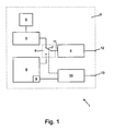
- An in Fig. 1 1 as a whole has a semiconductor component arranged in a component housing semiconductor chip 2 into which a magnetic field-sensitive sensor element 3, namely a Hall plate, and an evaluation device 4 are integrated therefor.
- a power source 5 is integrated, which is connected for feeding a Hall plate current in the sensor element 3 with this.
- the semiconductor component 1 has an operating switching device 6, by means of which it can be brought into a first and a second operating mode.
- a measurement signal output dependent on the magnetic flux density passing through the sensor element 3 is applied to a measuring signal output of the sensor element 3.
- the operation switching device 6 has a switching element 7, which connects the measuring signal output to an input terminal 11 of the evaluation device 4 in the first mode.
- the input terminal 11 is connected to a terminal 12, not shown in detail in the drawing, which is externally accessible to the component housing.
- the switching element 7 is switched such that the signal path between the measuring signal output of the sensor element 3 and the input terminal 11 of the evaluation device 4 is interrupted.
- the input terminal 11 is connected via the switching element 7 to a test signal output of a test signal source 8.
- the test signal source 8 is integrated in the semiconductor chip 2.
- the test signal is generated by means of an external test signal source and applied to the input terminal 11 of the evaluation device 4 via connection contacts provided on the semiconductor component.
- the test signal source 8 has a non-volatile data memory 9, in which a parameter for the sensitivity of the sensor element 3 is stored.
- the characteristic quantity is determined by measurement in the production of the semiconductor wafer from which the semiconductor chip of the sensor element 3 is produced.
- the semiconductor wafer has taps for connecting a measuring current source with the help of the measuring current source, an electric current is generated and fed via the taps in the sensor element 3.
- the voltage drop caused by the current flow in the sensor element 3 is measured, and from the current and the voltage drop, the electrical resistance of the sensor element is determined.
- This is stored in the data memory 9, which may be a PROM, for example.
- the test signal source 8 has an adjusting device not shown in the drawing, by means of which the amplitude of the test signal is adjustable.
- the adjusting device is connected via a serial interface 10 to an external terminal 13 of the semiconductor device 1.
- nominal values for a magnetic flux density to be simulated can be transmitted to the setting device by means of a test device connected to the external connection 13.
- the amplitude of the test signal is adjusted such that the test signal corresponds to the measurement signal of the sensor element 3, which would be present at the input terminal 11 of the evaluation device, if the semiconductor device 1 would be operated in the first mode and the sensor element 3 in a magnetic field, the magnetic Flux density corresponds to the setpoint.
- the test signal source 8 therefore, the measurement signal of the sensor element 3 can be reproduced exactly.
- the interface 10 is connected to an operating mode switching device 6 for this purpose.
- the sensor element 3 is insensitive to magnetic fields in the second operating mode.
- the operating switching device 6 has a first switching element 7a via which the current source 5 is connected to a Hall plate current connection of the sensor element 3.
- the first switching element 7a is connected such that the sensor element 3 is traversed by a Hall plate current.
- the second mode of operation the flow of current to the Hall plate power connections is interrupted.
- the operating switching device 6 further has a second switching element 7b, which is arranged in the signal path between the test signal output of the test signal source and the input terminal 11 of the evaluation device 4.
- a second switching element 7b which is arranged in the signal path between the test signal output of the test signal source and the input terminal 11 of the evaluation device 4.
- the signal path between the test signal output and the input terminal 11 of the evaluation device 4 is interrupted, and in the second operating mode the test signal output is connected to the input terminal 11 of the evaluation device 4.
Abstract
Description
Die Erfindung betrifft ein Halbleiterbauelement, dos auf einem Halbleiterchip mindestens ein Sensorelement zum Messen einer physikalischen Größe und eine Auswerteeinrichtung aufweist. Außerdem betrifft die Erfindung ein Verfahren zum Testen eines solchen Halbleiterbauelements.The invention relates to a semiconductor component, which has on a semiconductor chip at least one sensor element for measuring a physical quantity and an evaluation device. Moreover, the invention relates to a method for testing such a semiconductor device.
Ein derartiges Halbleiterbauelement, das als Sensorelement einen Magnetfeldsensor aufweist, ist aus
Des Weiteren sind aus der
Es besteht deshalb die Aufgabe, ein Halbleiterbauelement der eingangs genannten Art zu schaffen, das unter Verwendung eines Standard-Testgeräts auf einfache Weise getestet werden kann. Ferner besteht die Aufgabe, ein Verfahren der eingangs genannten Art zu schaffen, das auf einfache Weise eine Funktionsüberprüfung des Halbleiterbauelements ermöglicht.It is therefore an object to provide a semiconductor device of the type mentioned, which can be tested using a standard tester in a simple manner. Furthermore, the object is to provide a method of the type mentioned, which allows a simple way a functional verification of the semiconductor device.
Diese Aufgabe wird bezüglich des Halbleiterbauelements mit den Merkmalen des Patentanspruchs 1 gelöst. Erfindungsgemäß ist dabei das Halbleiterbauelement zwischen einer ersten und einer zweiten Betriebsart umschaltbar, wobei in der ersten Betriebsart das Sensorelement für die zu messende physikalische Größe empfindlich und ein Messsignalausgang des Sensorelements mit einem Eingangsanschluss der Auswerteeinrichtung verbunden ist, wobei in der zweiten Betriebsart das Sensorelement für die zu messende physikalische Größe unempfindlich und/oder der Signalpfad zwischen dem Messsignalausgang und dem Eingangsanschluss unterbrochen ist, wobei auf dem Halbleiterchip eine Testsignalquelle zur Erzeugung eines das Messsignal des Sensorelements simulierenden Testsignals angeordnet ist, und wobei die Testsignalquelle in der zweiten Betriebsart mit dem Eingangsanschluss der Auswerteeinrichtung verbunden oder verbindbar ist. In vorteilhafter Weise kann dann das Halbleiterbauelement in der zweiten Betriebsart getestet werden, ohne dass in der Umgebung des Halbleiterbauelements ein bestimmter Wert der physikalischen Größe, für deren Messung das Sensorelement vorgesehen ist, eingehalten oder eingestellt werden muss. Auch können aufwändige und komplizierte Maßnahmen zur Abschirmung des Sensorelements gegen die zu messende physikalische Größe eingespart werden, da das Sensorelement in der zweiten Betriebsart gegen die physikalische Größe unempfindlich ist. In der zweiten Betriebsart kann der elektrische Signalpfad zwischen dem Sensorelement und der Auswerteeinrichtung beispielsweise mittels mindestens eines Schaltelements unterbrochen sein. Bei einem Sensorelement, das für die Messung eine Betriebsspannung oder einen Betriebsstrom benötigt, ist es aber auch möglich, dass die Betriebsspannung oder der Betriebsstrom des Sensorelements in der zweiten Betriebsart abgeschaltet ist. Gegebenenfalls können auch beide Maßnahmen miteinander kombiniert sein. Dennoch kann die Auswerteeinrichtung getestet werden, indem mittels der Testsignalquelle anstelle des Sensor-Messsignals ein Testsignal in die Auswerteeinrichtung eingespeist und ein aufgrund des Testsignals von der Auswerteeinrichtung erzeugtes Ausgangssignal gemessen und gegebenenfalls mit einem vorgegebenen Referenzsignal verglichen wird. Somit kann die Auswerteeinrichtung mit Hilfe von in einer Halbleiterfabrik standardmäßig vorhandenen Testgeräten kostengünstig und schnell überprüft werden. Unter einer Auswerteeinrichtung wird die komplette elektrische Schaltung des Halbleiterbauelements mit Ausnahme des Sensorelements verstanden. Der Funktionstest des Sensorelements kann gegebenenfalls in einem früheren Fertigungsstadium des Halbleiterbauelements erfolgen, insbesondere wenn der Halbleiterchip des Sensorelements im Verbund mit anderen Halbleiterchips auf einem Wafer angeordnet ist. Ein entsprechendes Testverfahren für das Sensorelement ist in
Vorteilhaft ist, wenn die Testsignalquelle einen Datenspeicher aufweist, in dem mindestens eine dem Sensorelement zugeordnete Kenngröße abgelegt ist, und wenn die Testsignalquelle derart ausgestaltet ist, dass sie das Testsignal in Abhängigkeit von der mindestens einen Kenngröße erzeugt. In dem Datenspeicher kann als Kenngröße insbesondere die Empfindlichkeit, die das Sensorelement in der ersten Betriebsart gegenüber der zu messenden physikalischen Größe aufweist, abgelegt sein. Dadurch ist es möglich, mit Hilfe des Testsignals das Sensorsignal sehr genau nachzubilden und somit die Auswerteeinrichtung noch präziser zu testen.It is advantageous if the test signal source has a data memory in which at least one parameter assigned to the sensor element is stored, and if the test signal source is designed such that it generates the test signal as a function of the at least one parameter. In particular, the sensitivity that the sensor element has in the first operating mode with respect to the physical variable to be measured can be stored as a parameter in the data memory. This makes it possible to replicate the sensor signal with the help of the test signal very accurately and thus to test the evaluation even more precise.
Bei einer bevorzugten Ausgestaltung der Erfindung weist die Testsignalquelle eine Stelleinrichtung für das Testsignal auf, wobei ein Steuereingang der Stelleinrichtung zum Einstellen des Testsignals direkt oder indirekt über eine Ansteuereinrichtung mit einem externen Anschluss des Halbleiterbauelements verbunden ist. Somit können in der zweiten Betriebsart mit Hilfe eines an dem externen Anschluss angeschlossenen Testgeräts genau definierte Testsignalwerte an der Testsignalquelle abgerufen werden. Dabei ist es sogar möglich, die Testsignalwerte in Abhängigkeit von Vorgaben des Testgeräts und/oder in Abhängigkeit von der Antwort der Auswerteeinrichtung auf das Testsignal zu verändern.In a preferred embodiment of the invention, the test signal source on an adjusting device for the test signal, wherein a control input of the adjusting device for setting the test signal is connected directly or indirectly via a drive means with an external terminal of the semiconductor device. Thus, in the second mode, accurately defined test signal values at the test signal source can be retrieved using a test device connected to the external terminal. It is even possible to change the test signal values as a function of specifications of the test device and / or as a function of the response of the evaluation device to the test signal.
Bei einer zweckmäßigen Ausführungsbrm der Erfindung ist die Stelleinrichtung mit einer seriellen Schnittstelle verbunden, an die über den externen Anschluss Befehlescodes zum Einstellen des Testsignals übermittelbar sind. Die Datenverbindung zwischen dem an dem externen Anschluss angeschlossenen Textgerät und der Testsignalquelle ist dann weitgehend unempfindlich gegenüber EMV-Einstrahlung.In an expedient embodiment of the invention, the adjusting device is connected to a serial interface, to which command codes for setting the test signal can be transmitted via the external connection. The data connection between the text device connected to the external connection and the test signal source is then largely insensitive to EMC radiation.
Vorteilhaft ist, wenn die serielle Schnittstelle zum Umschalten der Betriebsart des Halbleiterbauelements mit einer Betriebsartenumschalteinrichtung verbunden ist. Dadurch kann an dem Halbleiterbauelement ein zusätzlicher externer Anschluss zum Umschalten der Betriebsart eingespart werden.It is advantageous if the serial interface for switching the operating mode of the semiconductor component is connected to an operating mode switching device. As a result, an additional external connection for switching over the operating mode can be saved on the semiconductor component.
Bei einer bevorzugten Ausgestaltung der Erfindung ist das Sensorelement ein Magnetfeldsensor, insbesondere ein Hall-Sensorelement. Es ist aber auch denkbar, dass das Sensorelement ein Drucksensor oder ein optischer Sensor ist.In a preferred embodiment of the invention, the sensor element is a magnetic field sensor, in particular a Hall sensor element. However, it is also conceivable that the sensor element is a pressure sensor or an optical sensor.
Die vorstehend genannte Aufgabe wird bezüglich des Verfahrens mit den Merkmalen des Patentanspruchs 8 gelöst. Vorteilhaft ist demgemäß ein Verfahren zum Testen eines Halbleiterbauelements, das auf einem Halbleiterchip mindestens ein Sensorelement zum Messen einer physikalischen Größe und eine über einen Signalpfad mit dem Sensorelement verbundene Auswerteeinrichtung aufweist, wobei der Signalpfad zwischen dem Sensorelement und der Auswerteeinrichtung während eines Funktionstests der Auswerteeinrichtung gesperrt oder unterbrochen wird, wobei ein das Messsignal des Sensorelements simulierendes Testsignal bereitgestellt und anstelle des Messsignals in die Auswerteeinrichtung eingespeist wird, und wobei mindestens ein von dem Testsignal abhängiges Ausgangssignal der Auswerteeinrichtung gemessen wird.The above object is achieved with respect to the method having the features of
Das gemessene Ausgangssignal kann dann gegebenenfalls mit einem Referenzsignal verglichen werden, wobei das Halbleiterbauelement in Abhängigkeit vom Ergebnis dieses Vergleichs als funktionsfähig eingestuft und für Messungen der physikalischen Größe freigegeben oder als nicht funktionsfähig ausgesondert wird. Da der Signalpfad zwischen dem Sensorelement und der Auswerteeinrichtung während eines Funktionstests gesperrt oder unterbrochen ist, kann die von dem Sensorelement abgetrennte restliche Schaltung des Halbleiterbauelements bei der Fertigung auf einfache Weise mittels eines Standardtestgeräts überprüft werden.The measured output signal can then optionally be compared with a reference signal, wherein the semiconductor device is classified as functional as a function of the result of this comparison and released for measurements of physical size or discarded as non-functional. Since the signal path between the sensor element and the evaluation device is blocked or interrupted during a functional test, the remaining circuit of the semiconductor component separated from the sensor element can easily be checked during manufacture by means of a standard test device.
Zum Testen des Sensorelements kann in dem Sensorelement ein Stromfluss erzeugt und der elektrische Widerstand des Sensorelements gemessen werden.For testing the sensor element, a current flow can be generated in the sensor element and the electrical resistance of the sensor element can be measured.
Somit kann das Sensorelement auf Funktion überprüft werden, ohne dass an dem Sensorelement ein bestimmter Wert der physikalischen Größe, für deren Messung das Sensorelement vorgesehen ist, erzeugt werden muss.Thus, the sensor element can be checked for function, without having to be generated on the sensor element, a certain value of the physical quantity, for the measurement of which the sensor element is provided.
Erwähnt werden soll noch, dass die Betriebsartenumschalteinrichtung mit einem vorzugsweise auf dem Halleiterchip und/oder an einem diesen umgrenzenden Bauelementgehäuse angeordneten elektrischen Anschlusskontakt verbunden sein kann, wobei die Betriebsart durch Anlegen eines externen elektrischen Potentials an den Anschlusskontakt und/oder durch Einspeisen eines elektrischen Stroms in den Anschlusskontakt umschaltbar ist. Dabei ist es sogar möglich, dass über den elektrischen Kontakt eine für den Betrieb des Halbleiterbauelements benötigte Versorgungsspannung an den Halbleiterchip anlegbar ist, und dass die Umschaltung der Betriebsart in Abhängigkeit von der Höhe der an den Anschlusskontakt angelegten Versorgungsspannung erfolgt.It should also be mentioned that the operating mode switching device can be connected to an electrical connection contact, which is preferably arranged on the semiconductor chip and / or on a component housing which surrounds it, wherein the operating mode is achieved by applying an external electrical potential to the connection contact and / or by supplying an electrical current the connection contact is switchable. In this case, it is even possible for a supply voltage required for the operation of the semiconductor component to be applied to the semiconductor chip via the electrical contact, and for the operating mode to be switched as a function of the level of the supply voltage applied to the connection contact.
Nachfolgend sind Ausführungsbeispiele der Erfindung anhand der Zeichnung näher erläutert. Es zeigen zum Teil stärker schematisiert:
- Fig. 1
- ein Blockschaltbild eines ersten Ausführungsbeispiels eines Halbleiterbauelements und
- Fig. 2
- ein Blockschaltbild eines zweiten Ausführungsbeispiels des Halbleiterbauelements.
- Fig. 1
- a block diagram of a first embodiment of a semiconductor device and
- Fig. 2
- a block diagram of a second embodiment of the semiconductor device.
Ein in
Das Halbleiterbauelement 1 weist eine Betriebsumschalteinrichtung 6 auf, mittels der es in eine erste und eine zweiten Betriebsart bringbar. In der ersten Betriebsart liegt an einem Messsignalausgang des Sensorelements 3 ein von der das Sensorelement 3 durchsetzenden magnetischen Flussdichte abhängiges Messsignal an.The
Wie in
In der zweiten Betriebsart ist das Schaltelement 7 derart geschaltet, dass der Signalpfad zwischen dem Messsignalausgang des Sensorelements 3 und dem Eingangsanschluss 11 der Auswerteeinrichtung 4 unterbrochen ist. Der Eingangsanschluss 11 ist über das Schaltelement 7 mit einem Testsignalausgang einer Testsignalquelle 8 verbunden. Die Testsignalquelle 8 ist in den Halbleiterchip 2 integriert. Es sind aber auch andere Ausführungsfbomen denkbar, bei denen das Testsignal mittels einer externen Testsignalquelle erzeugt und über an dem Halbleiterbauelement vorgesehene Anschlusskontakte an den Eingangsanschluss 11 der Auswerteeinrichtung 4 angelegt wird.In the second operating mode, the
Die Testsignalquelle 8 hat einen nicht flüchtigen Datenspeicher 9, in dem eine Kenngröße für die Empfindlichkeit des Sensorelements 3 abgelegt ist. Die Kenngrö-ße wird bei der Fertigung des Halbleiterwafers, aus dem der Halbleiterchip des Sensorelements 3 hergestellt wird, durch Messung ermittelt. Der Halbleiterwafer weist dazu Abgriffe zum Anschließen einer Messstromquelle auf Mit Hilfe der Messstromquelle wird ein elektrischer Strom erzeugt und über die Abgriffe in das Sensorelement 3 eingespeist. Der durch den Stromfluss in dem Sensorelement 3 hervorgerufene Spannungsabfall wird gemessen und aus dem Strom und dem Spannungsabfall wird der elektrische Widerstand des Sensorelements bestimmt. Dieser wird in dem Datenspeicher 9, der beispielsweise ein PROM sein kann, abgelegt.The
Die Testsignalquelle 8 hat eine in der Zeichnung nicht näher dargestellte Stelleinrichtung, mittels der die Amplitude des Testsignals einstellbar ist. Die Stelleinrichtung ist über eine serielle Schnittstelle 10 mit einem externen Anschluss 13 des Halbleiterbauelements 1 verbunden. Über die serielle Schnittstelle 10 können mittels eines an dem externen Anschluss 13 angeschlossenen Testgeräts Sollwerte für eine zu simulierende magnetische Flussdichte an die Stelleinrichtung übermittelt werden. In Abhängigkeit von dem jeweiligen Sollwert und der im Datenspeicher 8 abgelegten Kenngröße wird die Amplitude des Testsignals derart eingestellt, dass das Testsignal dem Messsignal des Sensorelements 3 entspricht, das am Eingangsanschluss 11 der Auswerteeinrichtung anliegen würde, wenn das Halbleiterbauelement 1 in der ersten Betriebsart betrieben würde und sich das Sensorelement 3 in einem Magnetfeld befände, dessen magnetische Flussdichte dem Sollwert entspricht. Mittels der Testsignalquelle 8 kann also das Messsignal des Sensorelements 3 genau nachgebildet werden.The
Über die Schnittstelle 10 kann auch die Betriebsart des Halbleiterbauelements 1 umgeschaltet werden. Die Schnittstelle 10 ist dazu mit einer Betriebsartenumschalteinrichtung 6 verbunden.Via the
Bei dem in
Die Betriebsumschalteinrichtung 6 hat ferner ein zweites Schaltelement 7b, das im Signalpfad zwischen dem Testsignalausgang der Testsignalquelle und dem Eingangsanschluss 11 der Auswerteeinrichtung 4 angeordnet ist. In der ersten Betriebsart ist der Signalpfad zwischen dem Testsignalausgang und dem Eingangsanschluss 11 der Auswerteeinrichtung 4 unterbrochen und in der zweiten Betriebsart ist der Testsignalausgang mit dem Eingangsanschluss 11 der Auswerteeinrichtung 4 verbunden. Wie bei dem Ausführungsbeispiel nach
Claims (7)
- Semiconductor component (1) comprising on a semiconductor chip (2) at least one sensor element (3) for measuring a physical magnitude and an evaluating device (4), wherein the semiconductor component (1) is switchable between a first operating mode and a second operating mode which are each so configured that in the first operating mode the sensor element (3) is connected by means of a current source (5) and is sensitive to the physical magnitude to be measured and a measurement signal output of the sensor element (3) is connected with an input connection (11) of the evaluating device (4), characterised in that a characteristic magnitude which the sensor element has by comparison with the magnitude to be measured is filed in a data memory (9) and in the second operating mode the sensor element (3) is insensitive to the physical magnitude to be measured, wherein the connection between the current source (5) and/or the signal path between the measurement signal output of the sensor element (3) and the input connection (11) is interrupted, and a test signal source (8) for producing a test signal simulating the measurement signal of the sensor element (3) in dependence on the stored characteristic magnitude is arranged on the semiconductor chip (2), and the test signal and the test signal source (8) in the second operating mode are connected with the input connection (11) of the evaluating device (4) in order to simulate the sensor signal with the help of the test signal.
- Semiconductor component (1) according to claim 1, characterised in that the test signal source (8) comprises a setting device for the test signal and that a control input of the setting device is, for setting the test signal, connected directly or indirectly by way of an activating device with an external connection of the semiconductor element (1).
- Semiconductor component (1) according to claim 1 or claim 2, characterised in that the setting device is connected with a serial interface (10) to which command codes for setting the test signal are transmissible by way of the external connection.
- Semiconductor component (1) according to any one of claims 1 to 3, characterised in that the serial interface (10) is, for switching over the operating mode of the semiconductor component (1), connected with an operating mode switch-over device (6).
- Semiconductor component (1) according to any one of claims 1 to 4, characterised in that the sensor element (3) is a magnetic field sensor, particularly a Hall sensor element.
- Method of testing a semiconductor component (1), which comprises on a semiconductor chip (2) at least one sensor element (3) for measuring a physical magnitude and an evaluating device (4) connected with the sensor element (3) by way of signal path, characterised in that in a first operating mode a characteristic magnitude which the sensor element has relative to the magnitude to be measured is filed in a memory and in a second operating mode the signal path between the sensor (3) and the evaluating device (4) is blocked or interrupted during a function test of the evaluating device (4), wherein a test signal simulating the measurement signal of the sensor element (3) is generated in dependence on the stored characteristic magnitude and is supplied to the evaluating device (4) instead of the measurement signal and wherein at least one output signal, which is dependent on the test signal, of the evaluating device (4) is measured.
- Method according to claim 6, characterised in that for testing the sensor element (3) a current flow in the sensor element (3) is produced and the electrical resistance of the sensor element (3) is measured.
Applications Claiming Priority (1)
| Application Number | Priority Date | Filing Date | Title |
|---|---|---|---|
| DE102007012214A DE102007012214A1 (en) | 2007-03-12 | 2007-03-12 | Semiconductor device and method for testing such |
Publications (3)
| Publication Number | Publication Date |
|---|---|
| EP1970720A2 EP1970720A2 (en) | 2008-09-17 |
| EP1970720A3 EP1970720A3 (en) | 2010-07-28 |
| EP1970720B1 true EP1970720B1 (en) | 2011-09-21 |
Family
ID=39495975
Family Applications (1)
| Application Number | Title | Priority Date | Filing Date |
|---|---|---|---|
| EP08004059A Active EP1970720B1 (en) | 2007-03-12 | 2008-03-05 | Semiconductor component and method for testing the same |
Country Status (4)
| Country | Link |
|---|---|
| US (1) | US8378672B2 (en) |
| EP (1) | EP1970720B1 (en) |
| AT (1) | ATE525661T1 (en) |
| DE (1) | DE102007012214A1 (en) |
Families Citing this family (12)
| Publication number | Priority date | Publication date | Assignee | Title |
|---|---|---|---|---|
| US8216317B2 (en) * | 2008-03-31 | 2012-07-10 | Stryker Spine | Spinal implant apparatus and methods |
| EP2163861A1 (en) * | 2008-09-12 | 2010-03-17 | Siemens Aktiengesellschaft | Process measuring device |
| EP2211147B1 (en) | 2009-01-23 | 2012-11-28 | Micronas GmbH | Method for testing the functionality of an electrical circuit |
| US8858637B2 (en) | 2010-09-30 | 2014-10-14 | Stryker Spine | Surgical implant with guiding rail |
| US8425529B2 (en) | 2010-09-30 | 2013-04-23 | Stryker Spine | Instrument for inserting surgical implant with guiding rail |
| US8603175B2 (en) | 2010-09-30 | 2013-12-10 | Stryker Spine | Method of inserting surgical implant with guiding rail |
| TWI439711B (en) * | 2011-10-03 | 2014-06-01 | Star Techn Inc | Switching matrix and testing system for semiconductor characteristic using the same |
| DE102011084283A1 (en) * | 2011-10-11 | 2013-04-11 | Robert Bosch Gmbh | Sensor unit and method for end-of-line programming of a sensor unit |
| US20140070831A1 (en) * | 2012-08-27 | 2014-03-13 | Advantest Corporation | System and method of protecting probes by using an intelligent current sensing switch |
| CN105093155B (en) * | 2015-08-25 | 2018-01-16 | 清华大学 | Micro-electromechanical system (MEMS) flux-gate magnetometer test system and its control method |
| BE1026732B1 (en) | 2018-10-26 | 2020-06-03 | Phoenix Contact Gmbh & Co | Measuring device |
| US11500010B2 (en) * | 2020-01-17 | 2022-11-15 | Texas Instruments Incorporated | Integrated circuit with current limit testing circuitry |
Family Cites Families (8)
| Publication number | Priority date | Publication date | Assignee | Title |
|---|---|---|---|---|
| DE4226224C2 (en) * | 1992-08-07 | 1994-05-26 | Texas Instruments Deutschland | Sensor responsive to the action of a force |
| DE19539458C2 (en) * | 1995-10-24 | 2001-03-15 | Bosch Gmbh Robert | Sensor with test input |
| DE19606826A1 (en) * | 1996-02-23 | 1997-08-28 | Knorr Bremse Electronic Gmbh | Method and device for checking a sensor |
| DE19858868C2 (en) * | 1998-12-19 | 2003-06-18 | Micronas Gmbh | Hall sensor |
| JP3835354B2 (en) * | 2001-10-29 | 2006-10-18 | ヤマハ株式会社 | Magnetic sensor |
| EP1637898A1 (en) * | 2004-09-16 | 2006-03-22 | Liaisons Electroniques-Mecaniques Lem S.A. | Continuously calibrated magnetic field sensor |
| DE102005028461A1 (en) | 2005-06-17 | 2006-12-28 | Micronas Gmbh | Method for testing a wafer, in particular Hall magnetic field sensor and wafer or Hall sensor |
| GB0620307D0 (en) * | 2006-10-16 | 2006-11-22 | Ami Semiconductor Belgium Bvba | Auto-calibration of magnetic sensor |
-
2007
- 2007-03-12 DE DE102007012214A patent/DE102007012214A1/en not_active Withdrawn
-
2008
- 2008-03-05 EP EP08004059A patent/EP1970720B1/en active Active
- 2008-03-05 AT AT08004059T patent/ATE525661T1/en active
- 2008-03-12 US US12/046,833 patent/US8378672B2/en active Active
Also Published As
| Publication number | Publication date |
|---|---|
| ATE525661T1 (en) | 2011-10-15 |
| DE102007012214A1 (en) | 2008-09-18 |
| EP1970720A2 (en) | 2008-09-17 |
| EP1970720A3 (en) | 2010-07-28 |
| US20080224694A1 (en) | 2008-09-18 |
| US8378672B2 (en) | 2013-02-19 |
Similar Documents
| Publication | Publication Date | Title |
|---|---|---|
| EP1970720B1 (en) | Semiconductor component and method for testing the same | |
| DE60122066T2 (en) | INTEGRATED CIRCUIT WITH TESTINTERFACE | |
| DE10011179B4 (en) | Method for determining the temperature of a semiconductor chip and semiconductor chip with temperature measuring arrangement | |
| DE69733789T2 (en) | High resolution power supply test system | |
| DE102008050018A1 (en) | Integrated magnetic sensor circuit with test lead | |
| DE102018119727A1 (en) | Testing MOS Circuit Breakers | |
| DE19917261C5 (en) | Electromagnetic flowmeter arrangement | |
| DE10146204A1 (en) | Circuit arrangement for the voltage supply of a two-wire sensor | |
| EP2623940B1 (en) | Testing of a measurement device assembly, corresponding measurement device assembly and test assembly | |
| DE112014002911T5 (en) | LED driver with comprehensive error protection | |
| DE69730116T2 (en) | METHOD FOR INSPECTION OF INTEGRATED CIRCUIT | |
| DE102017111410A1 (en) | Measurements in switching devices | |
| EP0250620A1 (en) | Method and device for electrically testing printed circuits | |
| DE10355116A1 (en) | Input and output circuit of an integrated circuit, method for testing an integrated circuit and integrated circuit with such input and output circuit | |
| DE102014014309A1 (en) | Method for testing a signal path | |
| DE102006040737A1 (en) | Electromagnetic valve output stage shunt recognizing device for motor vehicle`s brake circuit, has test pad arranged parallel to output stage-transitor to adjust current flow via coil, and comprising voltage comparator to measure variables | |
| DE102004049084A1 (en) | Sensor interface with integrated current measurement | |
| EP0705439B1 (en) | Process and device for testing an integrated circuit soldered on a board | |
| DE10341836B4 (en) | Test device for testing electrical circuits and method for parallel testing of electrical circuits | |
| WO2009100802A2 (en) | Circuit arrangement and method for testing a reset circuit | |
| DE102009050732B4 (en) | Digital matching in a microelectronic device | |
| DE102006017260A1 (en) | Circuit inspection procedure | |
| DE102007007339B4 (en) | Method and device for locating errors on electronic circuit boards | |
| DE102013210002A1 (en) | Method and apparatus for detecting a fault in a bridge circuit | |
| DE102018122314B3 (en) | Arrangement for determining a total current in a line |
Legal Events
| Date | Code | Title | Description |
|---|---|---|---|
| PUAI | Public reference made under article 153(3) epc to a published international application that has entered the european phase |
Free format text: ORIGINAL CODE: 0009012 |
|
| AK | Designated contracting states |
Kind code of ref document: A2 Designated state(s): AT BE BG CH CY CZ DE DK EE ES FI FR GB GR HR HU IE IS IT LI LT LU LV MC MT NL NO PL PT RO SE SI SK TR |
|
| AX | Request for extension of the european patent |
Extension state: AL BA MK RS |
|
| PUAL | Search report despatched |
Free format text: ORIGINAL CODE: 0009013 |
|
| AK | Designated contracting states |
Kind code of ref document: A3 Designated state(s): AT BE BG CH CY CZ DE DK EE ES FI FR GB GR HR HU IE IS IT LI LT LU LV MC MT NL NO PL PT RO SE SI SK TR |
|
| AX | Request for extension of the european patent |
Extension state: AL BA MK RS |
|
| 17P | Request for examination filed |
Effective date: 20110202 |
|
| AKX | Designation fees paid |
Designated state(s): AT BE BG CH CY CZ DE DK EE ES FI FR GB GR HR HU IE IS IT LI LT LU LV MC MT NL NO PL PT RO SE SI SK TR |
|
| GRAP | Despatch of communication of intention to grant a patent |
Free format text: ORIGINAL CODE: EPIDOSNIGR1 |
|
| RIC1 | Information provided on ipc code assigned before grant |
Ipc: G01R 35/00 20060101ALI20110426BHEP Ipc: G01R 33/00 20060101ALI20110426BHEP Ipc: G01R 31/28 20060101AFI20110426BHEP |
|
| GRAS | Grant fee paid |
Free format text: ORIGINAL CODE: EPIDOSNIGR3 |
|
| GRAA | (expected) grant |
Free format text: ORIGINAL CODE: 0009210 |
|
| AK | Designated contracting states |
Kind code of ref document: B1 Designated state(s): AT BE BG CH CY CZ DE DK EE ES FI FR GB GR HR HU IE IS IT LI LT LU LV MC MT NL NO PL PT RO SE SI SK TR |
|
| REG | Reference to a national code |
Ref country code: GB Ref legal event code: FG4D Free format text: NOT ENGLISH |
|
| REG | Reference to a national code |
Ref country code: CH Ref legal event code: EP |
|
| REG | Reference to a national code |
Ref country code: IE Ref legal event code: FG4D Free format text: LANGUAGE OF EP DOCUMENT: GERMAN |
|
| REG | Reference to a national code |
Ref country code: DE Ref legal event code: R096 Ref document number: 502008004923 Country of ref document: DE Effective date: 20111215 |
|
| REG | Reference to a national code |
Ref country code: NL Ref legal event code: VDEP Effective date: 20110921 |
|
| PG25 | Lapsed in a contracting state [announced via postgrant information from national office to epo] |
Ref country code: FI Free format text: LAPSE BECAUSE OF FAILURE TO SUBMIT A TRANSLATION OF THE DESCRIPTION OR TO PAY THE FEE WITHIN THE PRESCRIBED TIME-LIMIT Effective date: 20110921 Ref country code: LT Free format text: LAPSE BECAUSE OF FAILURE TO SUBMIT A TRANSLATION OF THE DESCRIPTION OR TO PAY THE FEE WITHIN THE PRESCRIBED TIME-LIMIT Effective date: 20110921 Ref country code: NO Free format text: LAPSE BECAUSE OF FAILURE TO SUBMIT A TRANSLATION OF THE DESCRIPTION OR TO PAY THE FEE WITHIN THE PRESCRIBED TIME-LIMIT Effective date: 20111221 Ref country code: SE Free format text: LAPSE BECAUSE OF FAILURE TO SUBMIT A TRANSLATION OF THE DESCRIPTION OR TO PAY THE FEE WITHIN THE PRESCRIBED TIME-LIMIT Effective date: 20110921 Ref country code: HR Free format text: LAPSE BECAUSE OF FAILURE TO SUBMIT A TRANSLATION OF THE DESCRIPTION OR TO PAY THE FEE WITHIN THE PRESCRIBED TIME-LIMIT Effective date: 20110921 |
|
| LTIE | Lt: invalidation of european patent or patent extension |
Effective date: 20110921 |
|
| PG25 | Lapsed in a contracting state [announced via postgrant information from national office to epo] |
Ref country code: LV Free format text: LAPSE BECAUSE OF FAILURE TO SUBMIT A TRANSLATION OF THE DESCRIPTION OR TO PAY THE FEE WITHIN THE PRESCRIBED TIME-LIMIT Effective date: 20110921 Ref country code: CY Free format text: LAPSE BECAUSE OF FAILURE TO SUBMIT A TRANSLATION OF THE DESCRIPTION OR TO PAY THE FEE WITHIN THE PRESCRIBED TIME-LIMIT Effective date: 20110921 Ref country code: GR Free format text: LAPSE BECAUSE OF FAILURE TO SUBMIT A TRANSLATION OF THE DESCRIPTION OR TO PAY THE FEE WITHIN THE PRESCRIBED TIME-LIMIT Effective date: 20111222 Ref country code: SI Free format text: LAPSE BECAUSE OF FAILURE TO SUBMIT A TRANSLATION OF THE DESCRIPTION OR TO PAY THE FEE WITHIN THE PRESCRIBED TIME-LIMIT Effective date: 20110921 |
|
| REG | Reference to a national code |
Ref country code: IE Ref legal event code: FD4D |
|
| PG25 | Lapsed in a contracting state [announced via postgrant information from national office to epo] |
Ref country code: IE Free format text: LAPSE BECAUSE OF FAILURE TO SUBMIT A TRANSLATION OF THE DESCRIPTION OR TO PAY THE FEE WITHIN THE PRESCRIBED TIME-LIMIT Effective date: 20110921 Ref country code: CZ Free format text: LAPSE BECAUSE OF FAILURE TO SUBMIT A TRANSLATION OF THE DESCRIPTION OR TO PAY THE FEE WITHIN THE PRESCRIBED TIME-LIMIT Effective date: 20110921 Ref country code: IS Free format text: LAPSE BECAUSE OF FAILURE TO SUBMIT A TRANSLATION OF THE DESCRIPTION OR TO PAY THE FEE WITHIN THE PRESCRIBED TIME-LIMIT Effective date: 20120121 Ref country code: SK Free format text: LAPSE BECAUSE OF FAILURE TO SUBMIT A TRANSLATION OF THE DESCRIPTION OR TO PAY THE FEE WITHIN THE PRESCRIBED TIME-LIMIT Effective date: 20110921 |
|
| PG25 | Lapsed in a contracting state [announced via postgrant information from national office to epo] |
Ref country code: IT Free format text: LAPSE BECAUSE OF FAILURE TO SUBMIT A TRANSLATION OF THE DESCRIPTION OR TO PAY THE FEE WITHIN THE PRESCRIBED TIME-LIMIT Effective date: 20110921 Ref country code: PT Free format text: LAPSE BECAUSE OF FAILURE TO SUBMIT A TRANSLATION OF THE DESCRIPTION OR TO PAY THE FEE WITHIN THE PRESCRIBED TIME-LIMIT Effective date: 20120123 Ref country code: EE Free format text: LAPSE BECAUSE OF FAILURE TO SUBMIT A TRANSLATION OF THE DESCRIPTION OR TO PAY THE FEE WITHIN THE PRESCRIBED TIME-LIMIT Effective date: 20110921 Ref country code: RO Free format text: LAPSE BECAUSE OF FAILURE TO SUBMIT A TRANSLATION OF THE DESCRIPTION OR TO PAY THE FEE WITHIN THE PRESCRIBED TIME-LIMIT Effective date: 20110921 Ref country code: PL Free format text: LAPSE BECAUSE OF FAILURE TO SUBMIT A TRANSLATION OF THE DESCRIPTION OR TO PAY THE FEE WITHIN THE PRESCRIBED TIME-LIMIT Effective date: 20110921 Ref country code: NL Free format text: LAPSE BECAUSE OF FAILURE TO SUBMIT A TRANSLATION OF THE DESCRIPTION OR TO PAY THE FEE WITHIN THE PRESCRIBED TIME-LIMIT Effective date: 20110921 |
|
| PLBE | No opposition filed within time limit |
Free format text: ORIGINAL CODE: 0009261 |
|
| STAA | Information on the status of an ep patent application or granted ep patent |
Free format text: STATUS: NO OPPOSITION FILED WITHIN TIME LIMIT |
|
| PG25 | Lapsed in a contracting state [announced via postgrant information from national office to epo] |
Ref country code: DK Free format text: LAPSE BECAUSE OF FAILURE TO SUBMIT A TRANSLATION OF THE DESCRIPTION OR TO PAY THE FEE WITHIN THE PRESCRIBED TIME-LIMIT Effective date: 20110921 |
|
| 26N | No opposition filed |
Effective date: 20120622 |
|
| BERE | Be: lapsed |
Owner name: MICRONAS G.M.B.H. Effective date: 20120331 |
|
| REG | Reference to a national code |
Ref country code: DE Ref legal event code: R097 Ref document number: 502008004923 Country of ref document: DE Effective date: 20120622 |
|
| PG25 | Lapsed in a contracting state [announced via postgrant information from national office to epo] |
Ref country code: MC Free format text: LAPSE BECAUSE OF NON-PAYMENT OF DUE FEES Effective date: 20120331 |
|
| REG | Reference to a national code |
Ref country code: CH Ref legal event code: PL |
|
| PG25 | Lapsed in a contracting state [announced via postgrant information from national office to epo] |
Ref country code: LI Free format text: LAPSE BECAUSE OF NON-PAYMENT OF DUE FEES Effective date: 20120331 Ref country code: BE Free format text: LAPSE BECAUSE OF NON-PAYMENT OF DUE FEES Effective date: 20120331 Ref country code: CH Free format text: LAPSE BECAUSE OF NON-PAYMENT OF DUE FEES Effective date: 20120331 |
|
| PG25 | Lapsed in a contracting state [announced via postgrant information from national office to epo] |
Ref country code: ES Free format text: LAPSE BECAUSE OF FAILURE TO SUBMIT A TRANSLATION OF THE DESCRIPTION OR TO PAY THE FEE WITHIN THE PRESCRIBED TIME-LIMIT Effective date: 20120101 |
|
| PG25 | Lapsed in a contracting state [announced via postgrant information from national office to epo] |
Ref country code: BG Free format text: LAPSE BECAUSE OF FAILURE TO SUBMIT A TRANSLATION OF THE DESCRIPTION OR TO PAY THE FEE WITHIN THE PRESCRIBED TIME-LIMIT Effective date: 20111221 |
|
| PG25 | Lapsed in a contracting state [announced via postgrant information from national office to epo] |
Ref country code: MT Free format text: LAPSE BECAUSE OF FAILURE TO SUBMIT A TRANSLATION OF THE DESCRIPTION OR TO PAY THE FEE WITHIN THE PRESCRIBED TIME-LIMIT Effective date: 20110921 |
|
| PG25 | Lapsed in a contracting state [announced via postgrant information from national office to epo] |
Ref country code: TR Free format text: LAPSE BECAUSE OF FAILURE TO SUBMIT A TRANSLATION OF THE DESCRIPTION OR TO PAY THE FEE WITHIN THE PRESCRIBED TIME-LIMIT Effective date: 20110921 |
|
| REG | Reference to a national code |
Ref country code: AT Ref legal event code: MM01 Ref document number: 525661 Country of ref document: AT Kind code of ref document: T Effective date: 20130305 |
|
| PG25 | Lapsed in a contracting state [announced via postgrant information from national office to epo] |
Ref country code: LU Free format text: LAPSE BECAUSE OF NON-PAYMENT OF DUE FEES Effective date: 20120305 |
|
| PG25 | Lapsed in a contracting state [announced via postgrant information from national office to epo] |
Ref country code: HU Free format text: LAPSE BECAUSE OF FAILURE TO SUBMIT A TRANSLATION OF THE DESCRIPTION OR TO PAY THE FEE WITHIN THE PRESCRIBED TIME-LIMIT Effective date: 20080305 |
|
| PG25 | Lapsed in a contracting state [announced via postgrant information from national office to epo] |
Ref country code: AT Free format text: LAPSE BECAUSE OF NON-PAYMENT OF DUE FEES Effective date: 20130305 |
|
| REG | Reference to a national code |
Ref country code: FR Ref legal event code: PLFP Year of fee payment: 9 |
|
| REG | Reference to a national code |
Ref country code: DE Ref legal event code: R082 Ref document number: 502008004923 Country of ref document: DE Representative=s name: KOCH-MUELLER PATENTANWALTSGESELLSCHAFT MBH, DE Ref country code: DE Ref legal event code: R081 Ref document number: 502008004923 Country of ref document: DE Owner name: TDK-MICRONAS GMBH, DE Free format text: FORMER OWNER: MICRONAS GMBH, 79108 FREIBURG, DE |
|
| REG | Reference to a national code |
Ref country code: FR Ref legal event code: PLFP Year of fee payment: 10 |
|
| REG | Reference to a national code |
Ref country code: FR Ref legal event code: PLFP Year of fee payment: 11 |
|
| REG | Reference to a national code |
Ref country code: FR Ref legal event code: CD Owner name: TDK-MICRONAS GMBH, DE Effective date: 20180717 |
|
| PGFP | Annual fee paid to national office [announced via postgrant information from national office to epo] |
Ref country code: GB Payment date: 20200323 Year of fee payment: 13 |
|
| PGFP | Annual fee paid to national office [announced via postgrant information from national office to epo] |
Ref country code: FR Payment date: 20200319 Year of fee payment: 13 |
|
| GBPC | Gb: european patent ceased through non-payment of renewal fee |
Effective date: 20210305 |
|
| PG25 | Lapsed in a contracting state [announced via postgrant information from national office to epo] |
Ref country code: FR Free format text: LAPSE BECAUSE OF NON-PAYMENT OF DUE FEES Effective date: 20210331 Ref country code: GB Free format text: LAPSE BECAUSE OF NON-PAYMENT OF DUE FEES Effective date: 20210305 |
|
| PGFP | Annual fee paid to national office [announced via postgrant information from national office to epo] |
Ref country code: DE Payment date: 20220620 Year of fee payment: 16 |