EP1967951A2 - Universal method and circuit for bus activity detection and system recovery - Google Patents
Universal method and circuit for bus activity detection and system recovery Download PDFInfo
- Publication number
- EP1967951A2 EP1967951A2 EP08101530A EP08101530A EP1967951A2 EP 1967951 A2 EP1967951 A2 EP 1967951A2 EP 08101530 A EP08101530 A EP 08101530A EP 08101530 A EP08101530 A EP 08101530A EP 1967951 A2 EP1967951 A2 EP 1967951A2
- Authority
- EP
- European Patent Office
- Prior art keywords
- bus
- activity
- time constant
- circuit
- condition
- Prior art date
- Legal status (The legal status is an assumption and is not a legal conclusion. Google has not performed a legal analysis and makes no representation as to the accuracy of the status listed.)
- Granted
Links
Images


Classifications
-
- G—PHYSICS
- G06—COMPUTING OR CALCULATING; COUNTING
- G06F—ELECTRIC DIGITAL DATA PROCESSING
- G06F11/00—Error detection; Error correction; Monitoring
- G06F11/07—Responding to the occurrence of a fault, e.g. fault tolerance
- G06F11/0703—Error or fault processing not based on redundancy, i.e. by taking additional measures to deal with the error or fault not making use of redundancy in operation, in hardware, or in data representation
- G06F11/0706—Error or fault processing not based on redundancy, i.e. by taking additional measures to deal with the error or fault not making use of redundancy in operation, in hardware, or in data representation the processing taking place on a specific hardware platform or in a specific software environment
- G06F11/0745—Error or fault processing not based on redundancy, i.e. by taking additional measures to deal with the error or fault not making use of redundancy in operation, in hardware, or in data representation the processing taking place on a specific hardware platform or in a specific software environment in an input/output transactions management context
-
- G—PHYSICS
- G06—COMPUTING OR CALCULATING; COUNTING
- G06F—ELECTRIC DIGITAL DATA PROCESSING
- G06F11/00—Error detection; Error correction; Monitoring
- G06F11/07—Responding to the occurrence of a fault, e.g. fault tolerance
- G06F11/0703—Error or fault processing not based on redundancy, i.e. by taking additional measures to deal with the error or fault not making use of redundancy in operation, in hardware, or in data representation
- G06F11/0751—Error or fault detection not based on redundancy
- G06F11/0754—Error or fault detection not based on redundancy by exceeding limits
- G06F11/0757—Error or fault detection not based on redundancy by exceeding limits by exceeding a time limit, i.e. time-out, e.g. watchdogs
-
- G—PHYSICS
- G06—COMPUTING OR CALCULATING; COUNTING
- G06F—ELECTRIC DIGITAL DATA PROCESSING
- G06F11/00—Error detection; Error correction; Monitoring
- G06F11/07—Responding to the occurrence of a fault, e.g. fault tolerance
- G06F11/0703—Error or fault processing not based on redundancy, i.e. by taking additional measures to deal with the error or fault not making use of redundancy in operation, in hardware, or in data representation
- G06F11/0793—Remedial or corrective actions
Definitions
- This invention relates to a universal method and circuit for bus activity detection and system recovery, particularly for microcomputer systems with a communication bus such as a television main-board's microcontroller.
- main-board and DVB module card communicate using universal asynchronous receiver-transmitter (UART).
- microcontroller and its peripherals communicate using inter-integrated circuit (12C).
- the microcontroller When using an (UART), the microcontroller has a dedicated register flag for monitoring the (UART) communication. If the communication fails after the system is reset or restarted, this flag is set and the microcontroller behaves according to this flag: reset the (DVB) microcontroller, re-transmit the last data, etc.
- the microcontroller When using (12C), the microcontroller, as being master, monitors its peripherals and the peripherals communicate as slave lCs. lf one of the peripherals fails to response to the master's command, the master resets it.
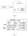
- microcontroller is assumed to have a dedicated register/block for monitoring the communication bus, as may be seen in Figure 1 .
- the microcontroller If the microcontroller has no dedicated part (register/block) for monitoring the bus activity, the system cannot detect the bus failure and take the correct action which causes a complete system crush.
- the microcontroller itself may also fail to do its jobs, such as configuring general-purpose input-output (GPIO) ports.
- GPIO general-purpose input-output
- the peripherals that need to be handled by these (GPIO) ports lack both the bus communication and (GPIO) action. This means that the system is in a failure state.
- watchdog system also referred as “watchdog timer”
- the system provides a software protection and resets the software in fault conditions; the faults due to hardware crushes can not be corrected by the watchdog system.
- the universal bus activity fault detection and resetting circuit comprises;
- the circuit further comprises means for determining said data period of the bus, sending said input data to said means for setting a time constant.
- the means for determining a time constant select one time constant value among a number of different given time constant values.
- said detecting means comprises an input circuit determining an average value of the data signal on said bus; an activity detection circuit receiving at the input said average value through said time constant, so as to generate said reset output if said average value is indicative of non activity on said bus.
- said average value indicative of non activity on said bus determines the conductivity condition of diode means which change the output level of said activity detection circuit through said time constant, so as to generate said reset output as a switching status of said activity detection circuit.
- the method further comprises a step of determining said input data relating to said data period of the bus.
- the present invention provides a detection and correction system which offers advantages of the state of the art. It offers universal bus fault detection and correction system for system crushes which is applicable to all kind of buses having periodic data transmission. Also, it does not require any specialized registers/blocks inside the microcontroller to generate an interrupt. Furthermore, this invention not only gives solutions to software crushes but also solves hardware based crushes.
- the object of the invention is to provide a universal method and circuit for bus activity and system recovery by monitoring the bus signal externally, detecting bus type, setting time constants for bus types and generating an output signal for the interrupt/reset pins of the microcontroller and/or the peripheral ICs in a fault condition.
- a further object of the invention is a universal bus activity fault detection and resetting method, comprising the steps of: determining a time constant for fault detection on the basis of input data relating to a data period of the bus; detecting a condition of activity or non activity on said bus, said detecting means generating a reset output on the basis of said time constant and said non activity condition.
- the circuit and method of the present invention can work for all systems having a microcontroller with an interrupt/reset port and a communication bus.
- the circuit is basically composed of five general block diagrams as depicted in Figure 3 .
- the main task of the present invention is to detect the period of used data transfer protocol, and then adjusting itself by means of setting time constant for fault detection within that particular bus, and to take action in case of error condition.
- the particular system can be used within systems having different periods for data transfer intervals. (such as UART and 12C)
- the first block is an emitter-follower circuit that is used as an input buffer.
- the aim of using an input-buffer is to make examinations on data bus signals without corrupting them.
- the second block which is called an "average measurement” takes the DC average of the incoming signal. This average value is used to control the transistor of the next block.
- the third block which is called an "output buffer” is used to buffer and invert the incoming signal.
- the fourth block gives an output (low or high) according to the input signal.
- the (A) labeled block provides the adjustment of the invention to any type of data bus which uses periodic signals.
- the invention After detecting the period of the bus, the invention enables one of the (B) labelled blocks to establish a dynamic time constant for bus fault detection system.
- the B blocks have different resistance values.
- the embodiment of the (A) labelled block is depicted in Figure 4 where according to periodical bus activities one of the resistor values inside the (B) labelled blocks are enabled and a universal bus fault detection circuit is established.
- the (B) labelled blocks have different resistance values to establish a bus fault detection and correction circuit applicable to all kind of buses.
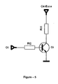
- the inner architecture of B blocks is depicted in figure 5 .
- the bus signal input is generally active low, i.e., in case of failure, the bus voltage level remains in high (idle) state.
- a periodicity in the bus signal is assumed. For example, a TV microcontroller transmits a SCL signal on the 12C line every t seconds.
- the time constant is adjusted manually and figures 7a, 7b , 7c and7d are sketched due to this fact; but the features of the invention vary the resistance values for different bus types and establishes a dynamic bus fault detection and correction system for all kinds of buses having periodical signal transmissions.
- the (A) labelled block depicted in Figure 4 is coupled to the bus for time constant detection, and (B) labelled blocks varies resistance values to establish a dynamic bus fault detection and correction system.
- the universal bus activity fault detection and resetting circuit comprises; means (C2, B1...Bn) for setting a time constant for fault detection on the basis of input data relating to said data period; detecting means (Q1, Q2, Q3, Q4) for detecting a condition of activity or non activity on said bus, said detecting means generating a reset output on the basis of said time constant and said non activity condition.
- the circuit further includes means (BLOCK A) for determining said data period of the bus.
- said means (C2, B1...Bn) for determining a time constant select one time constant value among a number of different given time constant values (B1...Bn).
- the universal bus activity fault detection and resetting circuit comprises means (BLOCK A) for determining the data period of the bus; means (C2, B1...Bn) for determining a time constant for fault detection on the basis of said data period; detecting means(Q1, Q2, Q3, Q4) for detecting a condition of activity or non activity on said bus, said detecting means generating a reset output on the basis of said time constant and said non activity condition.
- said detecting means comprises an input circuit (Q1, Q2, Q3) determining an average value of the data signal on said bus; and an activity detection circuit (Q4) receiving at the input said average value through said time constant, so as to generate said reset output if said average value is indicative of non activity on said bus. More preferably, said average value indicative of non activity on said bus determines the conductivity condition of diode means (D1) which change the output level of said activity detection circuit (Q4) through said time constant, so as to generate said reset output as a switching status of said activity detection circuit (Q4).
- D1 the conductivity condition of diode means
- the invention further includes a universal bus activity fault detection and resetting method, comprising the steps of: determining a time constant for fault detection on the basis of input data relating to a data period of the bus; detecting a condition of activity or non activity on said bus, said detecting means generating a reset output on the basis of said time constant and said non activity condition.
- the method further comprises a step of determining said input data relating to said data period of the bus.
Landscapes
- Engineering & Computer Science (AREA)
- Theoretical Computer Science (AREA)
- Quality & Reliability (AREA)
- Physics & Mathematics (AREA)
- General Engineering & Computer Science (AREA)
- General Physics & Mathematics (AREA)
- Debugging And Monitoring (AREA)
- Small-Scale Networks (AREA)
- Bus Control (AREA)
Abstract
Description
- This invention relates to a universal method and circuit for bus activity detection and system recovery, particularly for microcomputer systems with a communication bus such as a television main-board's microcontroller.
- Not only in computer, but also within consumer electronic goods, internal register flags are used to detect the bus activity. For example, in an IDTV set, main-board and DVB module card communicate using universal asynchronous receiver-transmitter (UART). In main-board itself, microcontroller and its peripherals (tuner, video processor, etc.) communicate using inter-integrated circuit (12C).
- When using an (UART), the microcontroller has a dedicated register flag for monitoring the (UART) communication. If the communication fails after the system is reset or restarted, this flag is set and the microcontroller behaves according to this flag: reset the (DVB) microcontroller, re-transmit the last data, etc.
- When using (12C), the microcontroller, as being master, monitors its peripherals and the peripherals communicate as slave lCs. lf one of the peripherals fails to response to the master's command, the master resets it.
- In both cases, microcontroller is assumed to have a dedicated register/block for monitoring the communication bus, as may be seen in
Figure 1 . - If the microcontroller has no dedicated part (register/block) for monitoring the bus activity, the system cannot detect the bus failure and take the correct action which causes a complete system crush.
- Moreover, it is also possible that when the bus communication fails, the microcontroller itself may also fail to do its jobs, such as configuring general-purpose input-output (GPIO) ports. In such a case, the peripherals that need to be handled by these (GPIO) ports, lack both the bus communication and (GPIO) action. This means that the system is in a failure state.
- The existence of fault detection and reset system is known from
US4434403 , where the clock signal should be checked periodically; whereas, within above described systems (just like 12C) the clock signal may not be continuous. The described technology is also not compatible with one sided data buses. - Another common system to overcome fault conditions occurred in data transmission systems is the watchdog system (also referred as "watchdog timer"). The system provides a software protection and resets the software in fault conditions; the faults due to hardware crushes can not be corrected by the watchdog system.
-
US4811200 describe the watchdog systems in which software and/or hardware is provided to monitor system operation and implement microprocessor resets in the event of improper system operation. In this document, the controllers within those systems require data bus activity responsive terminals and not compatible with various kind of buses, shown inFigure 2 . - As a conclusion, prior art systems require specialized registers/blocks inside the microcontroller to generate an interrupt. The existing systems for fault detection and correction for data buses are not compatible for all kind of bus systems. The main microcomputer is responsive of other peripherals, but complete system failure occurs if both the microcontroller and the peripheral fail to communicate.
- In accordance with the present invention, the universal bus activity fault detection and resetting circuit comprises;
- means for setting a time constant for fault detection on the basis of input data relating to a data period of the bus and,
- detecting means for detecting a condition of activity or non activity on said bus, said detecting means generating a reset output on the basis of said time constant and said non activity condition.
- Preferably the circuit further comprises means for determining said data period of the bus, sending said input data to said means for setting a time constant.
- Preferably, the means for determining a time constant select one time constant value among a number of different given time constant values.
- Preferably, said detecting means comprises an input circuit determining an average value of the data signal on said bus; an activity detection circuit receiving at the input said average value through said time constant, so as to generate said reset output if said average value is indicative of non activity on said bus.
- Preferably, said average value indicative of non activity on said bus determines the conductivity condition of diode means which change the output level of said activity detection circuit through said time constant, so as to generate said reset output as a switching status of said activity detection circuit.
- Preferably the method further comprises a step of determining said input data relating to said data period of the bus.
- The present invention provides a detection and correction system which offers advantages of the state of the art. It offers universal bus fault detection and correction system for system crushes which is applicable to all kind of buses having periodic data transmission. Also, it does not require any specialized registers/blocks inside the microcontroller to generate an interrupt. Furthermore, this invention not only gives solutions to software crushes but also solves hardware based crushes.
- The object of the invention is to provide a universal method and circuit for bus activity and system recovery by monitoring the bus signal externally, detecting bus type, setting time constants for bus types and generating an output signal for the interrupt/reset pins of the microcontroller and/or the peripheral ICs in a fault condition.
- A further object of the invention is a universal bus activity fault detection and resetting method, comprising the steps of: determining a time constant for fault detection on the basis of input data relating to a data period of the bus; detecting a condition of activity or non activity on said bus, said detecting means generating a reset output on the basis of said time constant and said non activity condition.
- Also it is aimed by this invention to provide a detection and correction system which gives solutions to software crushes but also solving hardware based crushes without requiring any specialized registers/blocks inside the microcontroller to generate an interrupt.
- The invention is illustrated in the appended figures, in which;
-
Figure 1 is an explanatory block diagram showing a microcontroller monitoring the communication bus. -
Figure 2 is a schematic block diagram showing a multiple microprocessor watchdog system. -
Figure 3 is an explanatory block diagram showing a circuit composed of five general block diagrams. -
Figure 4 is an explanatory block diagram showing an embodiment of the bus period detector. -
Figure 5 is an explanatory block diagram showing an inside architecture of (B) labelled blocks. -
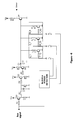
Figure 6 is an explanatory block diagram showing an establishment of the invention where t period is selected to be 1 second for practical applications. -
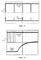
Figure 7a is a chart diagram showing the measured values where the emitter of (Q1) follows the input signal. -
Figure 7b is a chart diagram showing the measured values where the emitter of (Q2) follows the base. -
Figure 7c is a chart showing the measured values where the collector of (Q3) inversely follows the input signal. -
Figure 7d is a chart showing an example of bus failure. - The circuit and method of the present invention can work for all systems having a microcontroller with an interrupt/reset port and a communication bus.
- According to the invention, the circuit is basically composed of five general block diagrams as depicted in
Figure 3 . - The main task of the present invention is to detect the period of used data transfer protocol, and then adjusting itself by means of setting time constant for fault detection within that particular bus, and to take action in case of error condition.
- By means of having adjustable time constant within an error detection and correction system, the particular system can be used within systems having different periods for data transfer intervals. (such as UART and 12C)
- In
figure 3 , the first block is an emitter-follower circuit that is used as an input buffer. The aim of using an input-buffer is to make examinations on data bus signals without corrupting them. The second block which is called an "average measurement" takes the DC average of the incoming signal. This average value is used to control the transistor of the next block. The third block which is called an "output buffer" is used to buffer and invert the incoming signal. The fourth block gives an output (low or high) according to the input signal. The (A) labeled block provides the adjustment of the invention to any type of data bus which uses periodic signals. - After detecting the period of the bus, the invention enables one of the (B) labelled blocks to establish a dynamic time constant for bus fault detection system. The B blocks have different resistance values. The embodiment of the (A) labelled block is depicted in
Figure 4 where according to periodical bus activities one of the resistor values inside the (B) labelled blocks are enabled and a universal bus fault detection circuit is established. - As illustrated above, the (B) labelled blocks have different resistance values to establish a bus fault detection and correction circuit applicable to all kind of buses. The inner architecture of B blocks is depicted in
figure 5 . - In a communication and data transmission system, the bus signal input is generally active low, i.e., in case of failure, the bus voltage level remains in high (idle) state. In this method, a periodicity in the bus signal is assumed. For example, a TV microcontroller transmits a SCL signal on the 12C line every t seconds.
- In
Figure 6 an establishment of invention is represented where period t is selected to be 1 second for practical applications. - The principle of the invention will be explained step by step with the measured values.
- In
Figure 7a , the emitter of (Q1) follows the input signal, where (C1) and (R4) values determine the time constant. - Within the next step the emitter of (Q2) can now turn on and off (Q3) transistor; the measurement is shown in
Figure 7b . - The high values on the collector of (Q3) will turn on the (D1) diode. (C2) and resistance values in (B) labelled blocks in
Figure 6 determine the time constant for bus activity detection. The measurement is shown infigure 7c . - In this embodiment, the time constant is adjusted manually and
figures 7a, 7b ,7c and7d are sketched due to this fact; but the features of the invention vary the resistance values for different bus types and establishes a dynamic bus fault detection and correction system for all kinds of buses having periodical signal transmissions. The (A) labelled block depicted inFigure 4 is coupled to the bus for time constant detection, and (B) labelled blocks varies resistance values to establish a dynamic bus fault detection and correction system. - In the case of error, the high values on the collector of (Q3) will turn on the (D1) diode. As it is seen from
figure 4 , in a fault condition the system detects a fault and responses with an output. The output of the invention should be coupled to reset circuit of microprocessor or peripheral. An example of the bus failure is shown infigure 7d . - According to the first embodiment of the present invention, the universal bus activity fault detection and resetting circuit comprises; means (C2, B1...Bn) for setting a time constant for fault detection on the basis of input data relating to said data period; detecting means (Q1, Q2, Q3, Q4) for detecting a condition of activity or non activity on said bus, said detecting means generating a reset output on the basis of said time constant and said non activity condition.
- Preferably the circuit further includes means (BLOCK A) for determining said data period of the bus.
- Preferably, said means (C2, B1...Bn) for determining a time constant select one time constant value among a number of different given time constant values (B1...Bn).
- According to the second embodiment of the present invention, the universal bus activity fault detection and resetting circuit comprises means (BLOCK A) for determining the data period of the bus; means (C2, B1...Bn) for determining a time constant for fault detection on the basis of said data period; detecting means(Q1, Q2, Q3, Q4) for detecting a condition of activity or non activity on said bus, said detecting means generating a reset output on the basis of said time constant and said non activity condition.
- Preferably, said detecting means comprises an input circuit (Q1, Q2, Q3) determining an average value of the data signal on said bus; and an activity detection circuit (Q4) receiving at the input said average value through said time constant, so as to generate said reset output if said average value is indicative of non activity on said bus.
More preferably, said average value indicative of non activity on said bus determines the conductivity condition of diode means (D1) which change the output level of said activity detection circuit (Q4) through said time constant, so as to generate said reset output as a switching status of said activity detection circuit (Q4). - Therefore the invention further includes a universal bus activity fault detection and resetting method, comprising the steps of: determining a time constant for fault detection on the basis of input data relating to a data period of the bus; detecting a condition of activity or non activity on said bus, said detecting means generating a reset output on the basis of said time constant and said non activity condition.
- Preferably the method further comprises a step of determining said input data relating to said data period of the bus.
Claims (7)
- A universal bus activity fault detection and resetting circuit, characterized by comprising:• means (C2, B1...Bn) for setting a time constant for fault detection on the basis of input data relating to a data period of the bus;• detecting means (Q1, Q2, Q3, Q4) for detecting a condition of activity or non activity on said bus;• an output port for outputing a reset output signal generated on the basis of said time constant and said non activity condition.
- A circuit according to claim 1, characterized in that it further comprises means (BLOCK A) for determining said data period of the bus, sending said input data to said means (C2, B1...Bn) for setting a time constant.
- A circuit according to claim 1, characterized in that said means (C2, B1...Bn) for setting a time constant select one time constant value among a number of different given time constant values (B1...Bn).
- A circuit according to claim 1, characterized in that said detecting means comprise:• an input circuit (Q1, Q2, Q3) determining an average value of the data signal on said bus;• an activity detection circuit (Q4) receiving at the input said average value through said time constant, so as to generate said reset output if said average value is indicative of non activity on said bus.
- A circuit according to claim 4, characterized in that said average value indicative of non activity on said bus determines the conductivity condition of diode means (D1) which change the output level of said activity detection circuit (Q4) through said time constant, so as to generate said reset output as a switching status of said activity detection circuit (Q4).
- A universal bus activity fault detection and resetting method, characterized by comprising the following steps:• determining a time constant for fault detection on the basis of input data relating to a data period of the bus;• detecting a condition of activity or non activity on said bus;• said detecting means generating a reset output on the basis of said time constant and said non activity condition.
- A method according to claim 6, characterized in that it further comprises a step of determining said input data relating to said data period of the bus.
Applications Claiming Priority (1)
| Application Number | Priority Date | Filing Date | Title |
|---|---|---|---|
| TR2007/01134A TR200701134A2 (en) | 2007-02-23 | 2007-02-23 | Universal method and circuit for bus activity detection and system recovery. |
Publications (3)
| Publication Number | Publication Date |
|---|---|
| EP1967951A2 true EP1967951A2 (en) | 2008-09-10 |
| EP1967951A3 EP1967951A3 (en) | 2010-03-03 |
| EP1967951B1 EP1967951B1 (en) | 2013-03-06 |
Family
ID=39643883
Family Applications (1)
| Application Number | Title | Priority Date | Filing Date |
|---|---|---|---|
| EP08101530A Active EP1967951B1 (en) | 2007-02-23 | 2008-02-12 | Method and circuit for bus activity detection and system recovery |
Country Status (3)
| Country | Link |
|---|---|
| EP (1) | EP1967951B1 (en) |
| ES (1) | ES2410557T3 (en) |
| TR (1) | TR200701134A2 (en) |
Cited By (5)
| Publication number | Priority date | Publication date | Assignee | Title |
|---|---|---|---|---|
| EP3416059A1 (en) * | 2017-06-16 | 2018-12-19 | Vestel Elektronik Sanayi ve Ticaret A.S. | Hardware watchdog circuit and method |
| CN110275089A (en) * | 2018-03-13 | 2019-09-24 | 开利公司 | The detection of wiring trouble in universal serial bus connecting component |
| IT201900005822A1 (en) * | 2019-04-15 | 2020-10-15 | Phoenix Ict S R L S | GENERAL PURPOSE PERIPHERAL ADAPTER FOR COMPUTER |
| IT202100008723A1 (en) | 2021-04-08 | 2022-10-08 | Phoenix ICT | SYSTEM FOR THE SECURITY MANAGEMENT OF DIGITAL DOCUMENTS |
| CN116931474A (en) * | 2022-04-11 | 2023-10-24 | 中国航天科工飞航技术研究院(中国航天海鹰机电技术研究院) | Real-time fault diagnosis and protection method for EMIF parallel bus |
Citations (2)
| Publication number | Priority date | Publication date | Assignee | Title |
|---|---|---|---|---|
| US4434403A (en) | 1981-08-24 | 1984-02-28 | Burroughs Corporation | Universal reset circuit for digital circuitry |
| US4811200A (en) | 1987-05-12 | 1989-03-07 | Motorola, Inc. | Multiple microprocessor watchdog system |
Family Cites Families (4)
| Publication number | Priority date | Publication date | Assignee | Title |
|---|---|---|---|---|
| KR100252250B1 (en) * | 1996-06-28 | 2000-04-15 | 윤종용 | System recovery device |
| US6018803A (en) * | 1996-12-17 | 2000-01-25 | Intel Corporation | Method and apparatus for detecting bus utilization in a computer system based on a number of bus events per sample period |
| US6003146A (en) * | 1997-11-10 | 1999-12-14 | Honeywell Inc. | Method and apparatus of applying CRC to arinc 429 periodic data |
| US7627807B2 (en) * | 2005-04-26 | 2009-12-01 | Arm Limited | Monitoring a data processor to detect abnormal operation |
-
2007
- 2007-02-23 TR TR2007/01134A patent/TR200701134A2/en unknown
-
2008
- 2008-02-12 ES ES08101530T patent/ES2410557T3/en active Active
- 2008-02-12 EP EP08101530A patent/EP1967951B1/en active Active
Patent Citations (2)
| Publication number | Priority date | Publication date | Assignee | Title |
|---|---|---|---|---|
| US4434403A (en) | 1981-08-24 | 1984-02-28 | Burroughs Corporation | Universal reset circuit for digital circuitry |
| US4811200A (en) | 1987-05-12 | 1989-03-07 | Motorola, Inc. | Multiple microprocessor watchdog system |
Cited By (6)
| Publication number | Priority date | Publication date | Assignee | Title |
|---|---|---|---|---|
| EP3416059A1 (en) * | 2017-06-16 | 2018-12-19 | Vestel Elektronik Sanayi ve Ticaret A.S. | Hardware watchdog circuit and method |
| CN110275089A (en) * | 2018-03-13 | 2019-09-24 | 开利公司 | The detection of wiring trouble in universal serial bus connecting component |
| EP3540601A3 (en) * | 2018-03-13 | 2019-09-25 | Carrier Corporation | Detection of wiring faults in serial bus connected components |
| IT201900005822A1 (en) * | 2019-04-15 | 2020-10-15 | Phoenix Ict S R L S | GENERAL PURPOSE PERIPHERAL ADAPTER FOR COMPUTER |
| IT202100008723A1 (en) | 2021-04-08 | 2022-10-08 | Phoenix ICT | SYSTEM FOR THE SECURITY MANAGEMENT OF DIGITAL DOCUMENTS |
| CN116931474A (en) * | 2022-04-11 | 2023-10-24 | 中国航天科工飞航技术研究院(中国航天海鹰机电技术研究院) | Real-time fault diagnosis and protection method for EMIF parallel bus |
Also Published As
| Publication number | Publication date |
|---|---|
| ES2410557T3 (en) | 2013-07-02 |
| EP1967951B1 (en) | 2013-03-06 |
| EP1967951A3 (en) | 2010-03-03 |
| TR200701134A2 (en) | 2008-09-22 |
Similar Documents
| Publication | Publication Date | Title |
|---|---|---|
| US7707459B2 (en) | Embedded systems debugging | |
| EP1967951B1 (en) | Method and circuit for bus activity detection and system recovery | |
| US7945711B2 (en) | Appparatus and method for controlling power to USB device | |
| US12314600B2 (en) | Complex programmable logic device and communication method | |
| CN111077763A (en) | Vehicle-mounted display device redundancy control method and device | |
| US20190052355A1 (en) | Network switching system | |
| US20040181708A1 (en) | Policy-based response to system errors occuring during os runtime | |
| EP3118749B1 (en) | System and method of monitoring a serial bus | |
| CN116320379A (en) | State monitoring method and device for vehicle camera, computer equipment and storage medium | |
| US10986556B2 (en) | Circuit for monitoring a data processing system | |
| US7631129B2 (en) | Computer monitoring system and monitoring method | |
| US7904771B2 (en) | Self-diagnostic circuit and self-diagnostic method for detecting errors | |
| US20120185723A1 (en) | Eftb unit, usb device with the eftb unit and method for resetting and reenumerating the usb device | |
| US11953975B2 (en) | Peripheral component interconnect express device error reporting optimization method and system capable of filtering error reporting messages | |
| US10606702B2 (en) | System, information processing apparatus, and method for rebooting a part corresponding to a cause identified | |
| US7378977B2 (en) | Current overload detecting system and method | |
| CN217606356U (en) | Switching control circuit, mainboard and electronic equipment | |
| CN110704219A (en) | Hardware fault reporting method and device and computer storage medium | |
| CN114153637B (en) | Servo system | |
| EP1222543B1 (en) | Method and device for improving the reliability of a computer system | |
| CN120353636B (en) | Dynamic repairing method, system, equipment, medium and product for abnormal functions of controller | |
| CN218918094U (en) | Starting-up abnormity detection circuit, device and system | |
| WO2021169476A1 (en) | Server expansion system, and power control method for same | |
| CN219351792U (en) | a terminal | |
| CN210776663U (en) | Bus management module |
Legal Events
| Date | Code | Title | Description |
|---|---|---|---|
| PUAI | Public reference made under article 153(3) epc to a published international application that has entered the european phase |
Free format text: ORIGINAL CODE: 0009012 |
|
| 17P | Request for examination filed |
Effective date: 20080303 |
|
| AK | Designated contracting states |
Kind code of ref document: A2 Designated state(s): AT BE BG CH CY CZ DE DK EE ES FI FR GB GR HR HU IE IS IT LI LT LU LV MC MT NL NO PL PT RO SE SI SK TR |
|
| AX | Request for extension of the european patent |
Extension state: AL BA MK RS |
|
| PUAL | Search report despatched |
Free format text: ORIGINAL CODE: 0009013 |
|
| AK | Designated contracting states |
Kind code of ref document: A3 Designated state(s): AT BE BG CH CY CZ DE DK EE ES FI FR GB GR HR HU IE IS IT LI LT LU LV MC MT NL NO PL PT RO SE SI SK TR |
|
| AX | Request for extension of the european patent |
Extension state: AL BA MK RS |
|
| 17Q | First examination report despatched |
Effective date: 20100219 |
|
| AKX | Designation fees paid |
Designated state(s): AT BE BG CH CY CZ DE DK EE ES FI FR GB GR HR HU IE IS IT LI LT LU LV MC MT NL NO PL PT RO SE SI SK TR |
|
| RTI1 | Title (correction) |
Free format text: METHOD AND CIRCUIT FOR BUS ACTIVITY DETECTION AND SYSTEM RECOVERY |
|
| RIC1 | Information provided on ipc code assigned before grant |
Ipc: G06F 11/07 20060101AFI20120828BHEP |
|
| GRAP | Despatch of communication of intention to grant a patent |
Free format text: ORIGINAL CODE: EPIDOSNIGR1 |
|
| GRAS | Grant fee paid |
Free format text: ORIGINAL CODE: EPIDOSNIGR3 |
|
| GRAA | (expected) grant |
Free format text: ORIGINAL CODE: 0009210 |
|
| AK | Designated contracting states |
Kind code of ref document: B1 Designated state(s): AT BE BG CH CY CZ DE DK EE ES FI FR GB GR HR HU IE IS IT LI LT LU LV MC MT NL NO PL PT RO SE SI SK TR |
|
| REG | Reference to a national code |
Ref country code: GB Ref legal event code: FG4D |
|
| REG | Reference to a national code |
Ref country code: AT Ref legal event code: REF Ref document number: 599974 Country of ref document: AT Kind code of ref document: T Effective date: 20130315 Ref country code: CH Ref legal event code: EP |
|
| REG | Reference to a national code |
Ref country code: IE Ref legal event code: FG4D |
|
| REG | Reference to a national code |
Ref country code: DE Ref legal event code: R096 Ref document number: 602008022651 Country of ref document: DE Effective date: 20130502 |
|
| REG | Reference to a national code |
Ref country code: ES Ref legal event code: FG2A Ref document number: 2410557 Country of ref document: ES Kind code of ref document: T3 Effective date: 20130702 |
|
| REG | Reference to a national code |
Ref country code: AT Ref legal event code: MK05 Ref document number: 599974 Country of ref document: AT Kind code of ref document: T Effective date: 20130306 |
|
| PG25 | Lapsed in a contracting state [announced via postgrant information from national office to epo] |
Ref country code: BG Free format text: LAPSE BECAUSE OF FAILURE TO SUBMIT A TRANSLATION OF THE DESCRIPTION OR TO PAY THE FEE WITHIN THE PRESCRIBED TIME-LIMIT Effective date: 20130606 Ref country code: AT Free format text: LAPSE BECAUSE OF FAILURE TO SUBMIT A TRANSLATION OF THE DESCRIPTION OR TO PAY THE FEE WITHIN THE PRESCRIBED TIME-LIMIT Effective date: 20130306 Ref country code: LT Free format text: LAPSE BECAUSE OF FAILURE TO SUBMIT A TRANSLATION OF THE DESCRIPTION OR TO PAY THE FEE WITHIN THE PRESCRIBED TIME-LIMIT Effective date: 20130306 Ref country code: NO Free format text: LAPSE BECAUSE OF FAILURE TO SUBMIT A TRANSLATION OF THE DESCRIPTION OR TO PAY THE FEE WITHIN THE PRESCRIBED TIME-LIMIT Effective date: 20130606 Ref country code: SE Free format text: LAPSE BECAUSE OF FAILURE TO SUBMIT A TRANSLATION OF THE DESCRIPTION OR TO PAY THE FEE WITHIN THE PRESCRIBED TIME-LIMIT Effective date: 20130306 |
|
| REG | Reference to a national code |
Ref country code: NL Ref legal event code: VDEP Effective date: 20130306 |
|
| REG | Reference to a national code |
Ref country code: LT Ref legal event code: MG4D |
|
| PG25 | Lapsed in a contracting state [announced via postgrant information from national office to epo] |
Ref country code: SI Free format text: LAPSE BECAUSE OF FAILURE TO SUBMIT A TRANSLATION OF THE DESCRIPTION OR TO PAY THE FEE WITHIN THE PRESCRIBED TIME-LIMIT Effective date: 20130306 Ref country code: LV Free format text: LAPSE BECAUSE OF FAILURE TO SUBMIT A TRANSLATION OF THE DESCRIPTION OR TO PAY THE FEE WITHIN THE PRESCRIBED TIME-LIMIT Effective date: 20130306 Ref country code: FI Free format text: LAPSE BECAUSE OF FAILURE TO SUBMIT A TRANSLATION OF THE DESCRIPTION OR TO PAY THE FEE WITHIN THE PRESCRIBED TIME-LIMIT Effective date: 20130306 Ref country code: GR Free format text: LAPSE BECAUSE OF FAILURE TO SUBMIT A TRANSLATION OF THE DESCRIPTION OR TO PAY THE FEE WITHIN THE PRESCRIBED TIME-LIMIT Effective date: 20130607 |
|
| PG25 | Lapsed in a contracting state [announced via postgrant information from national office to epo] |
Ref country code: BE Free format text: LAPSE BECAUSE OF FAILURE TO SUBMIT A TRANSLATION OF THE DESCRIPTION OR TO PAY THE FEE WITHIN THE PRESCRIBED TIME-LIMIT Effective date: 20130306 Ref country code: HR Free format text: LAPSE BECAUSE OF FAILURE TO SUBMIT A TRANSLATION OF THE DESCRIPTION OR TO PAY THE FEE WITHIN THE PRESCRIBED TIME-LIMIT Effective date: 20130306 |
|
| PG25 | Lapsed in a contracting state [announced via postgrant information from national office to epo] |
Ref country code: PT Free format text: LAPSE BECAUSE OF FAILURE TO SUBMIT A TRANSLATION OF THE DESCRIPTION OR TO PAY THE FEE WITHIN THE PRESCRIBED TIME-LIMIT Effective date: 20130708 Ref country code: NL Free format text: LAPSE BECAUSE OF FAILURE TO SUBMIT A TRANSLATION OF THE DESCRIPTION OR TO PAY THE FEE WITHIN THE PRESCRIBED TIME-LIMIT Effective date: 20130306 Ref country code: IS Free format text: LAPSE BECAUSE OF FAILURE TO SUBMIT A TRANSLATION OF THE DESCRIPTION OR TO PAY THE FEE WITHIN THE PRESCRIBED TIME-LIMIT Effective date: 20130706 Ref country code: SK Free format text: LAPSE BECAUSE OF FAILURE TO SUBMIT A TRANSLATION OF THE DESCRIPTION OR TO PAY THE FEE WITHIN THE PRESCRIBED TIME-LIMIT Effective date: 20130306 Ref country code: EE Free format text: LAPSE BECAUSE OF FAILURE TO SUBMIT A TRANSLATION OF THE DESCRIPTION OR TO PAY THE FEE WITHIN THE PRESCRIBED TIME-LIMIT Effective date: 20130306 Ref country code: RO Free format text: LAPSE BECAUSE OF FAILURE TO SUBMIT A TRANSLATION OF THE DESCRIPTION OR TO PAY THE FEE WITHIN THE PRESCRIBED TIME-LIMIT Effective date: 20130306 Ref country code: CZ Free format text: LAPSE BECAUSE OF FAILURE TO SUBMIT A TRANSLATION OF THE DESCRIPTION OR TO PAY THE FEE WITHIN THE PRESCRIBED TIME-LIMIT Effective date: 20130306 |
|
| PG25 | Lapsed in a contracting state [announced via postgrant information from national office to epo] |
Ref country code: PL Free format text: LAPSE BECAUSE OF FAILURE TO SUBMIT A TRANSLATION OF THE DESCRIPTION OR TO PAY THE FEE WITHIN THE PRESCRIBED TIME-LIMIT Effective date: 20130306 Ref country code: CY Free format text: LAPSE BECAUSE OF FAILURE TO SUBMIT A TRANSLATION OF THE DESCRIPTION OR TO PAY THE FEE WITHIN THE PRESCRIBED TIME-LIMIT Effective date: 20130306 |
|
| PLBE | No opposition filed within time limit |
Free format text: ORIGINAL CODE: 0009261 |
|
| STAA | Information on the status of an ep patent application or granted ep patent |
Free format text: STATUS: NO OPPOSITION FILED WITHIN TIME LIMIT |
|
| PG25 | Lapsed in a contracting state [announced via postgrant information from national office to epo] |
Ref country code: DK Free format text: LAPSE BECAUSE OF FAILURE TO SUBMIT A TRANSLATION OF THE DESCRIPTION OR TO PAY THE FEE WITHIN THE PRESCRIBED TIME-LIMIT Effective date: 20130306 |
|
| 26N | No opposition filed |
Effective date: 20131209 |
|
| REG | Reference to a national code |
Ref country code: DE Ref legal event code: R097 Ref document number: 602008022651 Country of ref document: DE Effective date: 20131209 |
|
| PG25 | Lapsed in a contracting state [announced via postgrant information from national office to epo] |
Ref country code: LU Free format text: LAPSE BECAUSE OF FAILURE TO SUBMIT A TRANSLATION OF THE DESCRIPTION OR TO PAY THE FEE WITHIN THE PRESCRIBED TIME-LIMIT Effective date: 20140212 Ref country code: MC Free format text: LAPSE BECAUSE OF FAILURE TO SUBMIT A TRANSLATION OF THE DESCRIPTION OR TO PAY THE FEE WITHIN THE PRESCRIBED TIME-LIMIT Effective date: 20130306 |
|
| REG | Reference to a national code |
Ref country code: CH Ref legal event code: PL |
|
| PG25 | Lapsed in a contracting state [announced via postgrant information from national office to epo] |
Ref country code: LI Free format text: LAPSE BECAUSE OF NON-PAYMENT OF DUE FEES Effective date: 20140228 Ref country code: CH Free format text: LAPSE BECAUSE OF NON-PAYMENT OF DUE FEES Effective date: 20140228 |
|
| REG | Reference to a national code |
Ref country code: IE Ref legal event code: MM4A |
|
| PG25 | Lapsed in a contracting state [announced via postgrant information from national office to epo] |
Ref country code: IE Free format text: LAPSE BECAUSE OF NON-PAYMENT OF DUE FEES Effective date: 20140212 |
|
| REG | Reference to a national code |
Ref country code: FR Ref legal event code: PLFP Year of fee payment: 9 |
|
| PG25 | Lapsed in a contracting state [announced via postgrant information from national office to epo] |
Ref country code: MT Free format text: LAPSE BECAUSE OF FAILURE TO SUBMIT A TRANSLATION OF THE DESCRIPTION OR TO PAY THE FEE WITHIN THE PRESCRIBED TIME-LIMIT Effective date: 20130306 |
|
| PG25 | Lapsed in a contracting state [announced via postgrant information from national office to epo] |
Ref country code: HU Free format text: LAPSE BECAUSE OF FAILURE TO SUBMIT A TRANSLATION OF THE DESCRIPTION OR TO PAY THE FEE WITHIN THE PRESCRIBED TIME-LIMIT; INVALID AB INITIO Effective date: 20080212 |
|
| REG | Reference to a national code |
Ref country code: FR Ref legal event code: PLFP Year of fee payment: 10 |
|
| REG | Reference to a national code |
Ref country code: FR Ref legal event code: PLFP Year of fee payment: 11 |
|
| PGFP | Annual fee paid to national office [announced via postgrant information from national office to epo] |
Ref country code: IT Payment date: 20210222 Year of fee payment: 14 Ref country code: FR Payment date: 20210224 Year of fee payment: 14 |
|
| PGFP | Annual fee paid to national office [announced via postgrant information from national office to epo] |
Ref country code: GB Payment date: 20210219 Year of fee payment: 14 Ref country code: DE Payment date: 20210217 Year of fee payment: 14 |
|
| PGFP | Annual fee paid to national office [announced via postgrant information from national office to epo] |
Ref country code: ES Payment date: 20210422 Year of fee payment: 14 |
|
| REG | Reference to a national code |
Ref country code: DE Ref legal event code: R119 Ref document number: 602008022651 Country of ref document: DE |
|
| GBPC | Gb: european patent ceased through non-payment of renewal fee |
Effective date: 20220212 |
|
| PG25 | Lapsed in a contracting state [announced via postgrant information from national office to epo] |
Ref country code: FR Free format text: LAPSE BECAUSE OF NON-PAYMENT OF DUE FEES Effective date: 20220228 |
|
| PG25 | Lapsed in a contracting state [announced via postgrant information from national office to epo] |
Ref country code: GB Free format text: LAPSE BECAUSE OF NON-PAYMENT OF DUE FEES Effective date: 20220212 Ref country code: DE Free format text: LAPSE BECAUSE OF NON-PAYMENT OF DUE FEES Effective date: 20220901 |
|
| REG | Reference to a national code |
Ref country code: ES Ref legal event code: FD2A Effective date: 20230329 |
|
| PG25 | Lapsed in a contracting state [announced via postgrant information from national office to epo] |
Ref country code: ES Free format text: LAPSE BECAUSE OF NON-PAYMENT OF DUE FEES Effective date: 20220213 |
|
| PG25 | Lapsed in a contracting state [announced via postgrant information from national office to epo] |
Ref country code: IT Free format text: LAPSE BECAUSE OF NON-PAYMENT OF DUE FEES Effective date: 20220212 |
|
| PGFP | Annual fee paid to national office [announced via postgrant information from national office to epo] |
Ref country code: TR Payment date: 20260211 Year of fee payment: 19 |