EP1965554A2 - Method and system for a digital polar transmitter - Google Patents
Method and system for a digital polar transmitter Download PDFInfo
- Publication number
- EP1965554A2 EP1965554A2 EP08003287A EP08003287A EP1965554A2 EP 1965554 A2 EP1965554 A2 EP 1965554A2 EP 08003287 A EP08003287 A EP 08003287A EP 08003287 A EP08003287 A EP 08003287A EP 1965554 A2 EP1965554 A2 EP 1965554A2
- Authority
- EP
- European Patent Office
- Prior art keywords
- signal
- digital
- input
- dac
- voltage
- Prior art date
- Legal status (The legal status is an assumption and is not a legal conclusion. Google has not performed a legal analysis and makes no representation as to the accuracy of the status listed.)
- Withdrawn
Links
Images



Classifications
-
- H—ELECTRICITY
- H04—ELECTRIC COMMUNICATION TECHNIQUE
- H04L—TRANSMISSION OF DIGITAL INFORMATION, e.g. TELEGRAPHIC COMMUNICATION
- H04L27/00—Modulated-carrier systems
- H04L27/32—Carrier systems characterised by combinations of two or more of the types covered by groups H04L27/02, H04L27/10, H04L27/18 or H04L27/26
- H04L27/34—Amplitude- and phase-modulated carrier systems, e.g. quadrature-amplitude modulated carrier systems
- H04L27/36—Modulator circuits; Transmitter circuits
- H04L27/361—Modulation using a single or unspecified number of carriers, e.g. with separate stages of phase and amplitude modulation
Definitions
- Certain embodiments of the invention relate to communication networks. More specifically, certain embodiments of the invention relate to a method and system for a digital polar transmitter.
- Polar Modulation is related to inphase (I) and quadrature (Q) modulation in the same way that polar coordinates are related to the Cartesian coordinate system.
- I and Q modulation the orthogonal I and Q components of an RF signal are converted to a phasor representation comprising an amplitude component and a phase component.
- the combined I and Q signal may be generated with one phase change and one amplitude change, whereas separate I and Q modulation may require amplitude and phase modulation for each channel, especially for non-constant envelope modulation modes.
- the I and Q modulation approach may require good linearity of the power amplifier, often leading to power inefficient designs that suffer from parameter variability due to factors such as temperature.
- polar modulation may allow the use of very efficient and non-linear amplifier designs for non-constant envelope modulation schemes.
- an input may be represented as a phase modulation (PM) signal and an amplitude modulation (AM) signal.
- the PM signal may be input to a direct digital frequency synthesizer (DDFS).
- the DDFS may utilize the PM signal to generate a sequence binary numbers, each represented by a plurality of bits, which comprise a least significant bit (LSB) and a most significant bit (MSB). Each binary number may be converted to a corresponding voltage level. Thus, the corresponding sequence of voltage levels may form a representation of an analog signal.
- the analog signal may be input to a power amplifier (PA) circuit.
- PA power amplifier
- the AM signal may be input to the PA circuit.
- the PA circuit may utilize the AM signal to modify the amplitude of the input analog signal.
- the PA circuit is typically a non-linear amplifier, for example a Class C amplifier.
- the amplified analog signal may then be transmitted from the conventional polar modulation transmitter.
- a method and system for a digital polar transmitter substantially as shown in and/or described in connection with at least one of the figures, as set forth more completely in the claims.
- a method for generating signals in a wireless communication system comprising:
- FIG. 1 is a diagram of a polar modulation transmitter with a programmable-step-size digital to analog converter, in accordance with an embodiment of the invention.
- FIG. 2A is a diagram of an exemplary digital to analog converter circuit with binary weighted current sources, in accordance with an embodiment of the invention.
- FIG. 2B is a diagram of an exemplary digital to analog converter circuit with a configurable bias voltage, in accordance with an embodiment of the invention.
- FIG. 3 is a diagram of an exemplary signal illustrating step size programmability based on amplitude modulation information in a polar modulation transmitter, in accordance with an embodiment of the invention.
- FIG. 4 is a flow chart illustrating exemplary steps for a digital polar modulation transmitter with programmable-step-size digital to analog signal conversion, in accordance with an embodiment of the invention.
- Certain embodiments of the invention may be found in a method and system for a digital polar transmitter.
- Various embodiments of the invention may comprise a digital to analog converter (DAC), which converts input binary numbers to voltage levels that may be determined based on an amplitude modulation (AM) input signal. Consequently, the corresponding difference in voltage levels between consecutive binary numbers in a sequence (referred to as a "step size") may vary based on the AM input signal.
- DAC digital to analog converter
- AM amplitude modulation
- step size the corresponding difference in voltage levels between consecutive binary numbers in a sequence
- the power amplifier (PA) circuit may comprise a linear amplifier.
- FIG. 1 is a diagram of a polar modulation transmitter with a programmable-step-size digital to analog converter, in accordance with an embodiment of the invention.
- the digital polar transmitter 100 may comprise an accumulator 102, a digital to analog converter (DAC) 104, a PA 106, a processor 108, a memory 109, and an antenna 110.
- the accumulator 102 may be a part of a DDFS 103.
- the accumulator 102 and DAC 104 may be part of a DDFS 105.
- the DDFS 103 and/or 105 may be fabricated utilizing a deep submicron process such as a 45 nanometer (nm) deep submicron process.
- the 45 nanometer (nm) deep submicron process may be a 45 nanometer (nm) deep submicron CMOS process.
- the DDFS 103 and/or 105 may be enabled to generate high frequency signals that may facilitate polar modulation.
- the accumulator 102 may comprise suitable logic, circuitry and/or code that may enable generation of a sequence of binary numbers.
- Each binary number may comprise a least significant bit (LSB) and a most significant bit (MSB).
- the sequence of binary numbers may comprise values from 0 to 2 n -1, where n may be equal to the number of bits contained in each binary number.
- the operation of the accumulator 102 may be such that upon reaching a value 2 n -1 the next number in the sequence may be 0 with the sequence continuing.
- the set of numbers from 0 to 2 n -1 may represent a period of the sequence.
- the accumulator 102 may receive an input signal upon which the value of n may be determined.
- the input signal may be a phase modulation (PM) signal. Consequently, the value for n may be determined by the PM input signal.
- the period of the sequence of binary numbers generated by the accumulator 102 may be programmable based on the PM input signal.
- the DAC 104 may comprise suitable logic, circuitry and/or code that may enable generation of an analog output signal based on a sequence of input binary numbers.
- the DAC 104 may generate a corresponding analog voltage level for each input binary number.
- the number of distinct analog voltage levels may be equal to the number of distinct binary numbers in the input sequence.
- the DAC 104 may receive an input control signal upon which the corresponding analog voltage level for each input binary number may be determined.
- the input control signal may be an AM signal.
- the corresponding analog voltage level for a given binary input number may be determined based on the input AM signal.
- the corresponding analog voltage level for each other distinct binary input number in a sequence may also be determined based on the input AM signal.
- the step size, corresponding to the difference in corresponding analog voltage levels between consecutive binary input numbers in the sequence may be determined based on the input AM signal. Consequently, various embodiments of the invention may comprise a DAC that enables a programmable step size based on an input control signal.
- the PA circuit 106 may comprise suitable logic, circuitry and/or code that may enable amplification of input signals to generate a transmitted output signal of sufficient signal power (as measured by dBm, for example) for transmission via a wireless communication medium.
- the PA circuit may comprise a linear amplifier circuit.
- the PA circuit 106 may receive an analog input signal and generate a transmitted output signal, which is transmitted via the antenna 110.
- the processor 108 may comprise suitable logic, circuitry and/or code, which, in the context of the present application, may enable generation of AM and PM signals based on a received input signal.
- the received input signal may comprise an inphase (I) component, and a quadrature-phase (Q) component.
- the AM and PM signals may be generated based on the magnitudes of the I and Q components, and the relative phase relationship between I and Q component signals.
- the memory 109 may comprise suitable logic, circuitry and/or code that may enable storage and/or retrieval of data and/or code.
- the memory 109 may utilize any of a plurality of storage medium technologies, such as volatile memory, for example random access memory (RAM), and/or non-volatile memory, for example electrically erasable programmable read only memory (EEPROM).
- volatile memory for example random access memory (RAM)
- non-volatile memory for example electrically erasable programmable read only memory (EEPROM).
- EEPROM electrically erasable programmable read only memory
- the memory 109 may enable storage of code and/or data that enables generation of AM and PM signals based on a received input signal.
- the processor 108 may receive a quadrature input signal.
- the quadrature input signal may comprise an I component and a Q component.
- the processor 108 may compute corresponding AM and PM signals based on the I and Q components of the received quadrature input signal.
- the AM and/or PM signals may be digital signals, each carrying data in binary words.
- the PM signal may be sent to the accumulator 102, and the AM signal sent to the DAC 104.
- the accumulator 102 may utilize the PM signal to determine a modulus value n(PM) based on the PM signal. Consequently, the accumulator may generate a sequence of binary numbers: 0, 1, ..., 2 n(PM) , 0, 1, ..., 2 n(PM) , 0, 1,...
- the period of the sequence of binary numbers may be represented by the subsequence of binary numbers comprising 0, 1, ..., 2 n(PM) .
- the DAC 104 may receive the sequence of binary numbers as binary words, each comprising a plurality of bits. Each binary word may comprise an LSB and an MSB. The DAC 104 may utilize the binary word and the input AM signal to determine a corresponding analog voltage level. In various embodiments of the invention, the DAC 104 may utilize an entry in binary weighted current sources that increase or decrease a bias current level based on input AM signal data. In an exemplary embodiment of the invention, when the bias current level is determined, the analog voltage level corresponding to an input binary number may be determined by summing voltage contributions for each nonzero-valued bit in the input binary number. In another exemplary embodiment of the invention, when the bias current level may be determined, the analog voltage level corresponding to an input binary number may be determined by summing voltage contributions for each zero-valued bit in the input binary number.
- the analog voltage level, summed from voltage contributions for each bit in a given input binary number, may increase when the bias current level increases, and may decrease when the bias current level decreases. Consequently, the analog voltage level for a given input binary number may be programmable based on the input AM signal.
- a consecutive binary number in a sequence, b k+1 may be determined by incrementing the value of the given input binary number.
- b k + 1 b k + 1
- the corresponding analog voltage level generated by the DAC 104 may be represented by V a (b k , AM), which indicates that the analog voltage level may be determined based on the input binary number and the AM input signal.
- the step size Size Step may also change.
- the DAC 104 may enable a programmable step size based on the input AM signal.
- the DAC 104 may generate an analog output signal V out based on the sequence of corresponding analog voltage levels generated in response to the input binary sequence received from the accumulator 102.
- the analog signal may be input to the PA circuit 106, which may amplify the input analog signal to generate an analog output signal, RF out , which may be transmitted in a wireless communication medium via the antenna 110.
- the PA circuit 106 may comprise a linear amplifier.
- FIG. 2A is a diagram of an exemplary digital to analog converter circuit with binary weighted current sources, in accordance with an embodiment of the invention.
- a DAC 200 may represent an embodiment of the DAC 104 shown in FIG. 1 .
- the DAC 200 may comprise a plurality of selector switches 202 and 212, a plurality of current sources 204a, 204b, 204c, 214a, 214b and 214c, a plurality of contact switches 206a, 206b, 206c, 216a, 216b and 216c, an operational amplifier 222, and a resistor 224.
- the bits b 1 , ..., and b n may indicate bits in an input binary number to the DAC 200, where b 1 may represent the LSB and b n may represent the MSB.
- the bits c 1 , ..., and c m may indicate bits in an input control word to the DAC 200, for example, bits generated from the AM input signal to the DAC 200.
- the selector switch 202 may be configured in an OPEN or CLOSED state based on the input bit b 1 .
- the selector switch 202 may be configured to couple the node labeled N 1 to ground when in an OPEN state, or to the current sources 204a, 204b and 204c when in a CLOSED state.
- the current flowing through the selector switch 202, I bias_1 may be equal to the sum of current supplied by the current sources 204a, 204b and 204c.
- the contact switch 206a may be configured in an OPEN or CLOSED state based on the control bit c 1 .
- the contact switch 206a may enable the current source 204a to supply a current level, I 1,1 , which is nonzero when in a CLOSED state.
- I 1,1 a current level
- an open circuit condition may exist in which case the current source 204a may supply a current level of zero.
- the contact switch 206b may be configured in an OPEN or CLOSED state based on the control bit c 2 .
- the contact switch 206b may enable the current source 204b to supply a current level, I 1,2 , which may be nonzero when in a CLOSED state. In instance when the contact switch 206b may be in an OPEN state the current source 204b may supply a current level of zero.
- the contact switch 206c may be configured in an OPEN or CLOSED state based on the control bit c m .
- the contact switch 206c may enable the current source 204c to supply a current level, I 1,m , which may be nonzero when in a CLOSED state. In instances when the contact switch 206c may be in an OPEN state the current source 204b may supply a current level of zero.
- the selector switch 212 may be configured in an OPEN or CLOSED state based on the input bit b n .
- the selector switch 212 may be configured to couple the node labeled N 1 to ground when in an OPEN state, or to the current sources 214a, 214b and 214c when in a CLOSED state.
- the current flowing through the selector switch 212, I bias_n may be equal to the sum of current supplied by the current sources 214a, 214b and 214c.
- the contact switch 216a may be configured in an OPEN or CLOSED state based on the control bit c 1 .
- the contact switch 216a may enable the current source 214a to supply a current level, I n,1 , which is nonzero when in a CLOSED state. In instance when the contact switch 216a may be in an OPEN state the current source 214a may supply a current level of zero.
- the contact switch 216b may be configured in an OPEN or CLOSED state based on the control bit c 2 .
- the contact switch 216b may enable the current source 214b to supply a current level, I n,2 , which is nonzero when in a CLOSED state. In instance when the contact switch 216b may be in an OPEN state the current source 214b may supply a current level of zero.
- the contact switch 216c may be configured in an OPEN or CLOSED state based on the control bit c m .
- the contact switch 216c may enable the current source 214c to supply a current level, I n,m , which is nonzero when in a CLOSED state.
- I n,m a current level of zero.
- the operational amplifier 222 and the resistor 224 may generate an output voltage at the node labeled N 2 based on an input voltage at the node labeled N 1 .
- the operational amplifier 222 and resistor 224 may represent a negative feedback circuit such that the voltage appearing at the node labeled N 1 may be the negative of the voltage appearing at the node labeled N 2 .
- an decrease in the voltage appearing at the node N 1 may correspond to an increase in the voltage appearing at the node N 1 .
- an increasingly negative voltage (or decrease in voltage) appearing at the node N 1 may correspond to an increasingly positive voltage (or increase in voltage) appearing at the node N 2 .
- the voltage appearing at the node N 1 may be determined based on a sum of individual current contributions I bias_1 , ..., I bias_n .
- the bias current I bias_1 may increase or decrease based on the input control word to the DAC 200.
- An increase in the bias current I bias_1 may result in a decrease in the voltage appearing at the node N 1 when the selector switch 202 is in a CLOSED state.
- the difference in the voltage level appearing at the node N 1 when the selector switch 202 may be in a CLOSED state, and the voltage level appearing at the node N 1 when the selector switch 202 may be in an OPEN state may correspondingly increase or decrease based on the input control word to the DAC 200.
- the difference in voltage level appearing at the node N 1 in response to the selector switch 202 toggling between a CLOSED state and an OPEN state may be referred to as a voltage step.
- the voltage step associated with the operation of the selector switch 202 may increase or decrease based on the input control word to the DAC 200.
- the bias current I bias-n may increase or decrease based on the input control word to the DAC 200.
- An increase in the bias current I bias_n may result in a decrease in the voltage appearing at the node N 1 when the selector switch 212 is in a CLOSED state.
- the difference in the voltage level appearing at the node N 1 when the selector switch 212 is in a CLOSED state, and the voltage level appearing at the node N 1 when the selector switch 212 may be in an OPEN state may correspondingly increase or decrease based on the input control word to the DAC 200.
- the voltage step size associated with the operation of the selector switch 212 may increase or decrease based on the input control word to the DAC 200.
- FIG. 2B is a diagram of an exemplary digital to analog converter circuit with a configurable bias voltage, in accordance with an embodiment of the invention.
- a DAC 270 may represent an embodiment of the DAC 104 shown in FIG. 1 .
- the DAC 270 may comprise a plurality of selector switches 203 and 213, a plurality of resistors 225, 205, 215 and 217, a DC to DC (DC/DC) voltage converter 264, and an operational amplifier 223.
- the operation amplifier 223 may be substantially similar to the operational amplifier 222.
- the operational amplifier 223 and resistor 225 may form a negative feedback circuit and may be substantially similar to the negative feedback circuit comprising the operational amplifier 222 and resistor 224.
- the DC/DC converter 264 may comprise suitable logic, circuitry and/or code that may enable conversion of an input supply voltage, V SS , to a bias voltage, V bias , based on an input control word to the DAC 270.
- the DC/DC converter 264 may comprise a switching regulator circuit.
- the selector switch 203 may be configured in an OPEN or CLOSED state based on the input bit b 1 .
- the selector switch 203 may be configured to couple the node labeled N 3 to ground when in an OPEN state, or to the resistor 205 when in a CLOSED state.
- the selector switch 213 may be configured in an OPEN or CLOSED state based on the input bit b n .
- the selector switch 213 may be configured to couple the node labeled N 3 to ground when in an OPEN state, or to the resistor 215 when in a CLOSED state.
- the resistors 205, 215 and 217 may comprise a portion of a resistor divider network that enables the voltage appearing at the node labeled N 3 to change in response to the opening or closing of individual selector switches 203 and 213.
- a voltage step may occur in the voltage appearing at the node N 3 in response to a toggling of the respective selector switches 203 and/or 213 between the CLOSED state and the OPEN state.
- the voltage step occurring at the node N 3 in response to the opening or closing of the selector switch 203 or 213 may be equivalent to the voltage step occurring at the node N 1 ( FIG. 2A ) in response to the opening or closing of the selector switch 202 or 212.
- the corresponding step size resulting from the operation of each of the respective switches 203 and/or 213 may be based on the voltage level appearing at the node labeled V bias .
- the voltage level appearing at the node V bias may increase or decrease based on the application of input control word to the DC/DC converter 264.
- the voltage step size associated with the operation of a selector switch 203 or 213 may increase or decrease based on the input control word to the DAC 270.
- FIG. 3 is a diagram of an exemplary signal illustrating step size programmability based on amplitude modulation information in a polar modulation transmitter, in accordance with an embodiment of the invention.
- the horizontal axis of the exemplary graph 300 shows time, which may be measured in relevant units (for example, milliseconds), while the vertical axis shows voltage level, which may also be measured in relevant units (for example, hundreds of millivolts).
- the value of the AM data may be represented AM 1
- the value of the PM data may be represented PM 1
- the step size may be represented s 1 .
- s 1 1 voltage unit
- the period of the binary number sequence is 8.
- the value of the AM data may be represented AM 2
- the value of the PM data may be represented PM 1
- the step size may be represented s 2
- the exemplary graph 300 may indicate that the period of the sequence of binary numbers remains the same between the first time interval and the second time interval
- the step size for the first time interval, s 1 is shown as being different from the step size for the second time interval, s 2 .
- s 2 2 voltage units.
- the change in the AM data from AM 1 in the first time interval, to AM 2 in the second time interval may result in a corresponding change in the step size for the DAC 104.
- the change in the AM value may correspond to a change in the amplitude of the analog output signal V out generated by the DAC 104.
- the value of the AM data may be represented AM 3
- the value of the PM data may be represented PM 1
- the step size may be represented s 3
- the exemplary graph 300 may indicate that the period of the sequence of binary numbers remains the same between the second time interval and the third time interval
- the step size for the second time interval, s 2 is shown as being different from the step size for the third time interval, s 3 .
- s 3 1.5 voltage units.
- the value of the AM data may be represented AM 1
- the value of the PM data may be represented PM 2
- the step size may be represented by s 1
- the exemplary graph 300 may indicate that the step size of the fourth time interval is equal to the step size in the first
- the period of the sequence of binary numbers in the fourth time interval may be different from the period of the sequence of binary numbers in the preceding time intervals.
- the change in PM value may correspond to a change in the phase of the analog signal V out generated by the DAC 104.
- the period of the binary number sequence during the fourth time interval is 16.
- FIG. 4 is a flow chart illustrating exemplary steps for a digital polar modulation transmitter with programmable-step-size digital to analog signal conversion, in accordance with an embodiment of the invention.
- the processor 108 may receive an input signal.
- the input signal may be a quadrature input signal.
- the processor 108 may generate AM and PM signals based on the input signal.
- the AM and/or PM signals may be digital signals.
- the accumulator 102 may select a digital signal phase based on the PM signal.
- the digital phase may correspond to a period of a sequence of binary numbers generated by the accumulator 102.
- the DAC 104 may generate a digital signal step size based on the AM signal.
- the step size may be determined as shown in equation [2], for example.
- the DAC 104 may generate an analog output signal V out .
- the PA 106 may amplify the analog output signal V out to generate an amplified signal RF out .
- the amplified signal RF out may be transmitted in a wireless communication medium via the antenna 110.
- Various embodiments of the invention may comprise a plurality of DAC circuit designs for which the analog voltage output, in response to an input binary number, may vary based on a bias current and/or bias voltage.
- various embodiments of the invention may be practiced in DAC circuits for which both a bias current and/or bias voltage may be controlled based on an input control word.
- the present invention may be realized in hardware, software, or a combination of hardware and software.
- the present invention may be realized in a centralized fashion in at least one computer system, or in a distributed fashion where different elements are spread across several interconnected computer systems. Any kind of computer system or other apparatus adapted for carrying out the methods described herein is suited.
- a typical combination of hardware and software may be a general-purpose computer system with a computer program that, when being loaded and executed, controls the computer system such that it carries out the methods described herein.
- the present invention may also be embedded in a computer program product, which comprises all the features enabling the implementation of the methods described herein, and which when loaded in a computer system is able to carry out these methods.
- Computer program in the present context means any expression, in any language, code or notation, of a set of instructions intended to cause a system having an information processing capability to perform a particular function either directly or after either or both of the following: a) conversion to another language, code or notation; b) reproduction in a different material form.
Landscapes
- Engineering & Computer Science (AREA)
- Computer Networks & Wireless Communication (AREA)
- Signal Processing (AREA)
- Amplifiers (AREA)
- Transmitters (AREA)
Abstract
Description
- NOT APPLICABLE.
- Certain embodiments of the invention relate to communication networks. More specifically, certain embodiments of the invention relate to a method and system for a digital polar transmitter.
- Polar Modulation is related to inphase (I) and quadrature (Q) modulation in the same way that polar coordinates are related to the Cartesian coordinate system. For polar modulation, the orthogonal I and Q components of an RF signal are converted to a phasor representation comprising an amplitude component and a phase component. In this way, the combined I and Q signal may be generated with one phase change and one amplitude change, whereas separate I and Q modulation may require amplitude and phase modulation for each channel, especially for non-constant envelope modulation modes. In addition, the I and Q modulation approach may require good linearity of the power amplifier, often leading to power inefficient designs that suffer from parameter variability due to factors such as temperature. In contrast, polar modulation may allow the use of very efficient and non-linear amplifier designs for non-constant envelope modulation schemes.
- In some conventional polar modulation transmitters, an input may be represented as a phase modulation (PM) signal and an amplitude modulation (AM) signal. The PM signal may be input to a direct digital frequency synthesizer (DDFS). The DDFS may utilize the PM signal to generate a sequence binary numbers, each represented by a plurality of bits, which comprise a least significant bit (LSB) and a most significant bit (MSB). Each binary number may be converted to a corresponding voltage level. Thus, the corresponding sequence of voltage levels may form a representation of an analog signal. The analog signal may be input to a power amplifier (PA) circuit.
- The AM signal may be input to the PA circuit. The PA circuit may utilize the AM signal to modify the amplitude of the input analog signal. The PA circuit is typically a non-linear amplifier, for example a Class C amplifier. The amplified analog signal may then be transmitted from the conventional polar modulation transmitter.
- Further limitations and disadvantages of conventional and traditional approaches will become apparent to one of skill in the art, through comparison of such systems with some aspects of the present invention as set forth in the remainder of the present application with reference to the drawings.
- A method and system for a digital polar transmitter, substantially as shown in and/or described in connection with at least one of the figures, as set forth more completely in the claims.
According to an aspect of the invention, a method is provided for generating signals in a wireless communication system, the method comprising: - amplitude modulating via a digital-to-analog converter, an input phase modulated signal; and
- generating via said digital-to-analog converter, an output signal comprising a variable step size.
- one or more circuits comprising at least a digital-to-analog converter, that enable amplitude modulation, via said digital-to-analog converter, of an input phase modulated signal; and
- said one or more circuits enable generation, via said digital-to-analog converter, of an output signal comprising a variable step size.
- These and other advantages, aspects and novel features of the present invention, as well as details of an illustrated embodiment thereof, will be more fully understood from the following description and drawings.
-
FIG. 1 is a diagram of a polar modulation transmitter with a programmable-step-size digital to analog converter, in accordance with an embodiment of the invention. -
FIG. 2A is a diagram of an exemplary digital to analog converter circuit with binary weighted current sources, in accordance with an embodiment of the invention. -
FIG. 2B is a diagram of an exemplary digital to analog converter circuit with a configurable bias voltage, in accordance with an embodiment of the invention. -
FIG. 3 is a diagram of an exemplary signal illustrating step size programmability based on amplitude modulation information in a polar modulation transmitter, in accordance with an embodiment of the invention. -
FIG. 4 is a flow chart illustrating exemplary steps for a digital polar modulation transmitter with programmable-step-size digital to analog signal conversion, in accordance with an embodiment of the invention. - Certain embodiments of the invention may be found in a method and system for a digital polar transmitter. Various embodiments of the invention may comprise a digital to analog converter (DAC), which converts input binary numbers to voltage levels that may be determined based on an amplitude modulation (AM) input signal. Consequently, the corresponding difference in voltage levels between consecutive binary numbers in a sequence (referred to as a "step size") may vary based on the AM input signal. Thus, various embodiments of the invention may comprise a programmable-step-size DAC in which the step size may be dynamically programmable based on the AM input signal. In various embodiments of the invention, the power amplifier (PA) circuit may comprise a linear amplifier.
-
FIG. 1 is a diagram of a polar modulation transmitter with a programmable-step-size digital to analog converter, in accordance with an embodiment of the invention. Referring toFIG. 1 , there is shown a digitalpolar transmitter 100. The digitalpolar transmitter 100 may comprise anaccumulator 102, a digital to analog converter (DAC) 104, aPA 106, aprocessor 108, amemory 109, and anantenna 110. In an exemplary embodiment of the invention, theaccumulator 102 may be a part of aDDFS 103. In another exemplary embodiment of the invention, theaccumulator 102 andDAC 104 may be part of aDDFS 105. TheDDFS 103 and/or 105 may be fabricated utilizing a deep submicron process such as a 45 nanometer (nm) deep submicron process. The 45 nanometer (nm) deep submicron process may be a 45 nanometer (nm) deep submicron CMOS process. In this regard, theDDFS 103 and/or 105 may be enabled to generate high frequency signals that may facilitate polar modulation. - The
accumulator 102 may comprise suitable logic, circuitry and/or code that may enable generation of a sequence of binary numbers. Each binary number may comprise a least significant bit (LSB) and a most significant bit (MSB). In an exemplary numerical representation, the sequence of binary numbers may comprise values from 0 to 2n-1, where n may be equal to the number of bits contained in each binary number. The operation of theaccumulator 102 may be such that upon reaching a value 2n-1 the next number in the sequence may be 0 with the sequence continuing. The set of numbers from 0 to 2n-1 may represent a period of the sequence. - The
accumulator 102 may receive an input signal upon which the value of n may be determined. In various embodiments of the invention, the input signal may be a phase modulation (PM) signal. Consequently, the value for n may be determined by the PM input signal. Thus, the period of the sequence of binary numbers generated by theaccumulator 102 may be programmable based on the PM input signal. - The
DAC 104 may comprise suitable logic, circuitry and/or code that may enable generation of an analog output signal based on a sequence of input binary numbers. TheDAC 104 may generate a corresponding analog voltage level for each input binary number. The number of distinct analog voltage levels may be equal to the number of distinct binary numbers in the input sequence. - The
DAC 104 may receive an input control signal upon which the corresponding analog voltage level for each input binary number may be determined. In various embodiments of the invention, the input control signal may be an AM signal. The corresponding analog voltage level for a given binary input number may be determined based on the input AM signal. In addition, the corresponding analog voltage level for each other distinct binary input number in a sequence may also be determined based on the input AM signal. Furthermore, the step size, corresponding to the difference in corresponding analog voltage levels between consecutive binary input numbers in the sequence may be determined based on the input AM signal. Consequently, various embodiments of the invention may comprise a DAC that enables a programmable step size based on an input control signal. - The
PA circuit 106 may comprise suitable logic, circuitry and/or code that may enable amplification of input signals to generate a transmitted output signal of sufficient signal power (as measured by dBm, for example) for transmission via a wireless communication medium. In various embodiments of the invention, the PA circuit may comprise a linear amplifier circuit. In various embodiments of the invention, thePA circuit 106 may receive an analog input signal and generate a transmitted output signal, which is transmitted via theantenna 110. - The
processor 108 may comprise suitable logic, circuitry and/or code, which, in the context of the present application, may enable generation of AM and PM signals based on a received input signal. The received input signal may comprise an inphase (I) component, and a quadrature-phase (Q) component. The AM and PM signals may be generated based on the magnitudes of the I and Q components, and the relative phase relationship between I and Q component signals. - The
memory 109 may comprise suitable logic, circuitry and/or code that may enable storage and/or retrieval of data and/or code. Thememory 109 may utilize any of a plurality of storage medium technologies, such as volatile memory, for example random access memory (RAM), and/or non-volatile memory, for example electrically erasable programmable read only memory (EEPROM). In the context of the present application, thememory 109 may enable storage of code and/or data that enables generation of AM and PM signals based on a received input signal. - In operation, the
processor 108 may receive a quadrature input signal. The quadrature input signal may comprise an I component and a Q component. Theprocessor 108 may compute corresponding AM and PM signals based on the I and Q components of the received quadrature input signal. The AM and/or PM signals may be digital signals, each carrying data in binary words. The PM signal may be sent to theaccumulator 102, and the AM signal sent to theDAC 104. Theaccumulator 102 may utilize the PM signal to determine a modulus value n(PM) based on the PM signal. Consequently, the accumulator may generate a sequence of binary numbers: 0, 1, ..., 2n(PM), 0, 1, ..., 2 n(PM), 0, 1,... The period of the sequence of binary numbers may be represented by the subsequence of binary numbers comprising 0, 1, ..., 2 n(PM). - The
DAC 104 may receive the sequence of binary numbers as binary words, each comprising a plurality of bits. Each binary word may comprise an LSB and an MSB. TheDAC 104 may utilize the binary word and the input AM signal to determine a corresponding analog voltage level. In various embodiments of the invention, theDAC 104 may utilize an entry in binary weighted current sources that increase or decrease a bias current level based on input AM signal data. In an exemplary embodiment of the invention, when the bias current level is determined, the analog voltage level corresponding to an input binary number may be determined by summing voltage contributions for each nonzero-valued bit in the input binary number. In another exemplary embodiment of the invention, when the bias current level may be determined, the analog voltage level corresponding to an input binary number may be determined by summing voltage contributions for each zero-valued bit in the input binary number. - In various embodiments of the invention, the analog voltage level, summed from voltage contributions for each bit in a given input binary number, may increase when the bias current level increases, and may decrease when the bias current level decreases. Consequently, the analog voltage level for a given input binary number may be programmable based on the input AM signal.
- For a given input binary number, bk, a consecutive binary number in a sequence, bk+1, may be determined by incrementing the value of the given input binary number. For example:

DAC 104 may be represented by Va(bk, AM), which indicates that the analog voltage level may be determined based on the input binary number and the AM input signal. As such, the step size for theDAC 104, SizeStep(AM), may be represented as in the following equation, for example:
- As shown in equation [2], when the analog voltage levels Va(bk, AM) and/or Va(bk+1, AM) change in response to changes in the AM signal, the step size SizeStep(AM) may also change. Thus, in various embodiments of the invention, the
DAC 104 may enable a programmable step size based on the input AM signal. - The
DAC 104 may generate an analog output signal Vout based on the sequence of corresponding analog voltage levels generated in response to the input binary sequence received from theaccumulator 102. The analog signal may be input to thePA circuit 106, which may amplify the input analog signal to generate an analog output signal, RFout, which may be transmitted in a wireless communication medium via theantenna 110. In various embodiments of the invention, thePA circuit 106 may comprise a linear amplifier. -
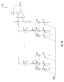
FIG. 2A is a diagram of an exemplary digital to analog converter circuit with binary weighted current sources, in accordance with an embodiment of the invention. Referring toFIG. 2A , there is shown aDAC 200. In various embodiments of the invention, theDAC 200 may represent an embodiment of theDAC 104 shown inFIG. 1 . TheDAC 200 may comprise a plurality of selector switches 202 and 212, a plurality ofcurrent sources contact switches operational amplifier 222, and aresistor 224. - In
FIG. 2A , the bits b1, ..., and bn may indicate bits in an input binary number to theDAC 200, where b1 may represent the LSB and bn may represent the MSB. The bits c1, ..., and cm may indicate bits in an input control word to theDAC 200, for example, bits generated from the AM input signal to theDAC 200. - The
selector switch 202 may be configured in an OPEN or CLOSED state based on the input bit b1. Theselector switch 202 may be configured to couple the node labeled N1 to ground when in an OPEN state, or to thecurrent sources selector switch 202 may be configured in a CLOSED state, the current flowing through theselector switch 202, Ibias_1, may be equal to the sum of current supplied by thecurrent sources - The
contact switch 206a may be configured in an OPEN or CLOSED state based on the control bit c1. Thecontact switch 206a may enable thecurrent source 204a to supply a current level, I1,1, which is nonzero when in a CLOSED state. In instance when thecontact switch 206a may be in an OPEN state, an open circuit condition may exist in which case thecurrent source 204a may supply a current level of zero. - The
contact switch 206b may be configured in an OPEN or CLOSED state based on the control bit c2. Thecontact switch 206b may enable thecurrent source 204b to supply a current level, I1,2, which may be nonzero when in a CLOSED state. In instance when thecontact switch 206b may be in an OPEN state thecurrent source 204b may supply a current level of zero. - The
contact switch 206c may be configured in an OPEN or CLOSED state based on the control bit cm. Thecontact switch 206c may enable thecurrent source 204c to supply a current level, I1,m, which may be nonzero when in a CLOSED state. In instances when thecontact switch 206c may be in an OPEN state thecurrent source 204b may supply a current level of zero. - Based on the foregoing, the current Ibias_1 may be represented as in the following equation:

- The
selector switch 212 may be configured in an OPEN or CLOSED state based on the input bit bn. Theselector switch 212 may be configured to couple the node labeled N1 to ground when in an OPEN state, or to thecurrent sources selector switch 212 may be configured in a CLOSED state, the current flowing through theselector switch 212, Ibias_n, may be equal to the sum of current supplied by thecurrent sources - The
contact switch 216a may be configured in an OPEN or CLOSED state based on the control bit c1. Thecontact switch 216a may enable thecurrent source 214a to supply a current level, In,1, which is nonzero when in a CLOSED state. In instance when thecontact switch 216a may be in an OPEN state thecurrent source 214a may supply a current level of zero. - The
contact switch 216b may be configured in an OPEN or CLOSED state based on the control bit c2. Thecontact switch 216b may enable thecurrent source 214b to supply a current level, In,2, which is nonzero when in a CLOSED state. In instance when thecontact switch 216b may be in an OPEN state thecurrent source 214b may supply a current level of zero. - The
contact switch 216c may be configured in an OPEN or CLOSED state based on the control bit cm. Thecontact switch 216c may enable thecurrent source 214c to supply a current level, In,m, which is nonzero when in a CLOSED state. In instances when thecontact switch 216c may be in an OPEN state thecurrent source 214b may supply a current level of zero. - Based on the foregoing, the current Ibias_n may be represented as in the following equation:

- The
operational amplifier 222 and theresistor 224 may generate an output voltage at the node labeled N2 based on an input voltage at the node labeled N1. Theoperational amplifier 222 andresistor 224 may represent a negative feedback circuit such that the voltage appearing at the node labeled N1 may be the negative of the voltage appearing at the node labeled N2. Thus, an decrease in the voltage appearing at the node N1 may correspond to an increase in the voltage appearing at the node N1. For example, an increasingly negative voltage (or decrease in voltage) appearing at the node N1 may correspond to an increasingly positive voltage (or increase in voltage) appearing at the node N2. - The voltage appearing at the node N1 may be determined based on a sum of individual current contributions Ibias_1, ..., Ibias_n. The total current flowing through the node N1, Ibias, may be represented as in the following equation:

current sources 
values 1≤i≤n and:
values 1≤j≤m. - According to equation [3], the bias current Ibias_1 may increase or decrease based on the input control word to the
DAC 200. An increase in the bias current Ibias_1 may result in a decrease in the voltage appearing at the node N1 when theselector switch 202 is in a CLOSED state. The difference in the voltage level appearing at the node N1 when theselector switch 202 may be in a CLOSED state, and the voltage level appearing at the node N1 when theselector switch 202 may be in an OPEN state may correspondingly increase or decrease based on the input control word to theDAC 200. The difference in voltage level appearing at the node N1 in response to theselector switch 202 toggling between a CLOSED state and an OPEN state may be referred to as a voltage step. Thus, in various embodiments of the invention, the voltage step associated with the operation of theselector switch 202 may increase or decrease based on the input control word to theDAC 200. - According to equation [4], the bias current Ibias-n may increase or decrease based on the input control word to the
DAC 200. An increase in the bias current Ibias_n may result in a decrease in the voltage appearing at the node N1 when theselector switch 212 is in a CLOSED state. The difference in the voltage level appearing at the node N1 when theselector switch 212 is in a CLOSED state, and the voltage level appearing at the node N1 when theselector switch 212 may be in an OPEN state may correspondingly increase or decrease based on the input control word to theDAC 200. Thus, in various embodiments of the invention, the voltage step size associated with the operation of theselector switch 212 may increase or decrease based on the input control word to theDAC 200. -
FIG. 2B is a diagram of an exemplary digital to analog converter circuit with a configurable bias voltage, in accordance with an embodiment of the invention. Referring toFIG. 2B , there is shown aDAC 270. In various embodiments of the invention, theDAC 270 may represent an embodiment of theDAC 104 shown inFIG. 1 . TheDAC 270 may comprise a plurality of selector switches 203 and 213, a plurality ofresistors voltage converter 264, and anoperational amplifier 223. Theoperation amplifier 223 may be substantially similar to theoperational amplifier 222. Theoperational amplifier 223 andresistor 225 may form a negative feedback circuit and may be substantially similar to the negative feedback circuit comprising theoperational amplifier 222 andresistor 224. - The DC/
DC converter 264 may comprise suitable logic, circuitry and/or code that may enable conversion of an input supply voltage, VSS, to a bias voltage, Vbias, based on an input control word to theDAC 270. In an exemplary embodiment of the invention, the DC/DC converter 264 may comprise a switching regulator circuit. - The
selector switch 203 may be configured in an OPEN or CLOSED state based on the input bit b1. Theselector switch 203 may be configured to couple the node labeled N3 to ground when in an OPEN state, or to theresistor 205 when in a CLOSED state. - The
selector switch 213 may be configured in an OPEN or CLOSED state based on the input bit bn. Theselector switch 213 may be configured to couple the node labeled N3 to ground when in an OPEN state, or to theresistor 215 when in a CLOSED state. - The
resistors selector switch FIG. 2A ) in response to the opening or closing of theselector switch respective switches 203 and/or 213 may be based on the voltage level appearing at the node labeled Vbias. The voltage level appearing at the node Vbias may increase or decrease based on the application of input control word to the DC/DC converter 264. Thus, in various embodiments of the invention, the voltage step size associated with the operation of aselector switch DAC 270. -
FIG. 3 is a diagram of an exemplary signal illustrating step size programmability based on amplitude modulation information in a polar modulation transmitter, in accordance with an embodiment of the invention. Referring toFIG. 3 , there is shown anexemplary graph 300 of an exemplary signal generated by theDAC 104 in response to a binary sequence of numbers received from theaccumulator 102. The horizontal axis of theexemplary graph 300 shows time, which may be measured in relevant units (for example, milliseconds), while the vertical axis shows voltage level, which may also be measured in relevant units (for example, hundreds of millivolts). As shown in theexemplary graph 300, during a first time interval between time instants indicated as t1 and t2, the value of the AM data may be represented AM1, while the value of the PM data may be represented PM1. During this first time interval, the step size may be represented s1. As shown in theexemplary graph 300, s1=1 voltage unit, and the period of the binary number sequence is 8. - During a second time interval between time instants indicated as t2 and t3, the value of the AM data may be represented AM2, while the value of the PM data may be represented PM1. During this second time interval, the step size may be represented s2. While the
exemplary graph 300 may indicate that the period of the sequence of binary numbers remains the same between the first time interval and the second time interval, the step size for the first time interval, s1, is shown as being different from the step size for the second time interval, s2. As shown in theexemplary graph 300, s2=2 voltage units. As shown in theexemplary graph 300, s2>s1. Thus, as shown in theexemplary graph 300, the change in the AM data from AM1 in the first time interval, to AM2 in the second time interval may result in a corresponding change in the step size for theDAC 104. The change in the AM value may correspond to a change in the amplitude of the analog output signal Vout generated by theDAC 104. - During a third time interval between time instants indicated as t3 and t4, the value of the AM data may be represented AM3, while the value of the PM data may be represented PM1. During this third time interval, the step size may be represented s3. While the
exemplary graph 300 may indicate that the period of the sequence of binary numbers remains the same between the second time interval and the third time interval, the step size for the second time interval, s2, is shown as being different from the step size for the third time interval, s3. As shown in theexemplary graph 300, s3=1.5 voltage units. As shown in theexemplary graph 300, s2>s3>s1. - During a fourth time interval between time instants indicated as t4 and t5, the value of the AM data may be represented AM1, while the value of the PM data may be represented PM2. During this fourth time interval, the step size may be represented by s1. While the
exemplary graph 300 may indicate that the step size of the fourth time interval is equal to the step size in the first, the period of the sequence of binary numbers in the fourth time interval may be different from the period of the sequence of binary numbers in the preceding time intervals. The change in PM value may correspond to a change in the phase of the analog signal Vout generated by theDAC 104. As shown in theexemplary graph 300, the period of the binary number sequence during the fourth time interval is 16. -
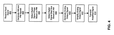
FIG. 4 is a flow chart illustrating exemplary steps for a digital polar modulation transmitter with programmable-step-size digital to analog signal conversion, in accordance with an embodiment of the invention. Referring toFIG. 4 , instep 402, theprocessor 108 may receive an input signal. The input signal may be a quadrature input signal. Instep 404, theprocessor 108 may generate AM and PM signals based on the input signal. The AM and/or PM signals may be digital signals. Instep 406, theaccumulator 102 may select a digital signal phase based on the PM signal. The digital phase may correspond to a period of a sequence of binary numbers generated by theaccumulator 102. In step 408, theDAC 104 may generate a digital signal step size based on the AM signal. The step size may be determined as shown in equation [2], for example. Instep 410, theDAC 104 may generate an analog output signal Vout. Instep 412, thePA 106 may amplify the analog output signal Vout to generate an amplified signal RFout. Instep 414, the amplified signal RFout may be transmitted in a wireless communication medium via theantenna 110. - Various embodiments of the invention may comprise a plurality of DAC circuit designs for which the analog voltage output, in response to an input binary number, may vary based on a bias current and/or bias voltage. In addition, various embodiments of the invention may be practiced in DAC circuits for which both a bias current and/or bias voltage may be controlled based on an input control word.
- Accordingly, the present invention may be realized in hardware, software, or a combination of hardware and software. The present invention may be realized in a centralized fashion in at least one computer system, or in a distributed fashion where different elements are spread across several interconnected computer systems. Any kind of computer system or other apparatus adapted for carrying out the methods described herein is suited. A typical combination of hardware and software may be a general-purpose computer system with a computer program that, when being loaded and executed, controls the computer system such that it carries out the methods described herein.
- The present invention may also be embedded in a computer program product, which comprises all the features enabling the implementation of the methods described herein, and which when loaded in a computer system is able to carry out these methods. Computer program in the present context means any expression, in any language, code or notation, of a set of instructions intended to cause a system having an information processing capability to perform a particular function either directly or after either or both of the following: a) conversion to another language, code or notation; b) reproduction in a different material form.
- While the present invention has been described with reference to certain embodiments, it will be understood by those skilled in the art that various changes may be made and equivalents may be substituted without departing from the scope of the present invention. In addition, many modifications may be made to adapt a particular situation or material to the teachings of the present invention without departing from its scope. Therefore, it is intended that the present invention not be limited to the particular embodiment disclosed, but that the present invention will include all embodiments falling within the scope of the appended claims.
Advantageously, said input phase modulated signal is generated based on a quadrature signal comprising an in-phase component and a quadrature-phase component.
Advantageously, the method further comprises dynamically varying said variable step size during operation of said digital-to-analog converter.
Advantageously, the method further comprises generating said output signal based on a sequence comprising a plurality of binary numbers.
Advantageously, the method further comprises generating one or more voltage levels in response to said sequence comprising said plurality of binary numbers.
Advantageously, the method further comprises dynamically controlling each of said generated one or more voltage levels based on an input control word.
Advantageously, a voltage difference between said generated one or more voltage levels corresponding to a current one of said plurality of binary words and said generated one or more voltage levels corresponding to a succeeding one of said plurality of binary words in said sequence is a voltage step.
Advantageously, the method further comprises dynamically controlling said voltage step based on an input control word.
Advantageously, the method further comprises generating said input control word based on an amplitude modulation signal.
Advantageously, the method further comprises dynamically controlling said voltage step by controlling a plurality of current source circuits.
Advantageously, the method further comprises controlling each of said plurality of current source circuits based on at least a portion of an input control word.
Advantageously, the method further comprises dynamically controlling said voltage step by controlling a voltage converter circuit.
Advantageously, the method further comprises controlling said voltage converter circuit based on an input control word.
Advantageously, the method further comprises generating said sequence based on a phase modulation signal.
Advantageously, the method further comprises amplifying said generated output signal to generate an RF signal that is transmitted via a wireless communication medium.
Advantageously, said amplifying is performed utilizing a linear amplifier circuit.
According to an aspect of the invention, a system is provided for generating signals in a wireless communication system, the system comprising:
Advantageously, said input phase modulated signal is generated based on a quadrature signal comprising an in-phase component and a quadrature-phase component.
Advantageously, said one or more circuits enable dynamic variation of said variable step size during operation of said digital-to-analog converter.
Advantageously, said one or more circuits enable generation of said output signal based on a sequence comprising a plurality of binary numbers.
Advantageously, said one or more circuits enable generation of one or more voltage levels in response to said sequence comprising said plurality of binary numbers.
Advantageously, said one or more circuits enable dynamic control of each of said generated one or more voltage levels based on an input control word.
Advantageously, a voltage difference between said generated one or more voltage levels corresponding to a current one of said plurality of binary words and said generated one or more voltage levels corresponding to a succeeding one of said plurality of binary words in said sequence is a voltage step.
Advantageously, said one or more circuits enable dynamic control of said voltage step based on an input control word.
Advantageously, said one or more circuits enable generation of said input control word based on an amplitude modulated signal.
Advantageously, said one or more circuits comprise a plurality of current sources, and enable dynamic control of said voltage step by controlling said plurality of current source circuits.
Advantageously, said one or more circuits enable control of each of said plurality of current source circuits based on at least a portion of an input control word.
Advantageously, said one or more circuits comprise a voltage converter circuit, and enable dynamic control of said voltage step by controlling said voltage converter circuit.
Advantageously, said one or more circuits enable control of said voltage converter circuit based on an input control word.
Advantageously, said one or more circuits enable generation of said sequence based on a phase modulation signal.
Advantageously, said one or more circuits enable amplification of said generated output signal to generate an RF signal that is transmitted via a wireless communication medium.
Advantageously, said one or more circuits comprise a linear amplifier circuit, and said amplifying is performed utilizing said linear amplifier circuit.
Claims (10)
- A method for generating signals in a wireless communication system, the method comprising:amplitude modulating via a digital-to-analog converter, an input phase modulated signal; andgenerating via said digital-to-analog converter, an output signal comprising a variable step size.
- The method according to claim 1, comprising generating said input phase modulated signal via a direct digital frequency synthesizer.
- The method according to claim 1, wherein said input phase modulated signal is generated based on a quadrature signal comprising an in-phase component and a quadrature-phase component.
- The method according to claim 1, comprising dynamically varying said variable step size during operation of said digital-to-analog converter.
- The method according to claim 1, comprising generating said output signal based on a sequence comprising a plurality of binary numbers.
- The method according to claim 5, comprising generating one or more voltage levels in response to said sequence comprising said plurality of binary numbers.
- A system for generating signals in a wireless communication system, the system comprising:one or more circuits comprising at least a digital-to-analog converter, that enable amplitude modulation, via said digital-to-analog converter, of an input phase modulated signal; andsaid one or more circuits enable generation, via said digital-to-analog converter, of an output signal comprising a variable step size.
- The system according to claim 7, wherein said one or more circuits comprise a direct digital frequency synthesizer, and enable generation of said input phase modulated signal via said direct digital frequency synthesizer.
- The system according to claim 7, wherein said input phase modulated signal is generated based on a quadrature signal comprising an in-phase component and a quadrature-phase component.
- The system according to claim 7, wherein said one or more circuits enable dynamic variation of said variable step size during operation of said digital-to-analog converter.
Applications Claiming Priority (1)
| Application Number | Priority Date | Filing Date | Title |
|---|---|---|---|
| US11/680,891 US8116387B2 (en) | 2007-03-01 | 2007-03-01 | Method and system for a digital polar transmitter |
Publications (2)
| Publication Number | Publication Date |
|---|---|
| EP1965554A2 true EP1965554A2 (en) | 2008-09-03 |
| EP1965554A3 EP1965554A3 (en) | 2013-11-06 |
Family
ID=39615868
Family Applications (1)
| Application Number | Title | Priority Date | Filing Date |
|---|---|---|---|
| EP08003287.3A Withdrawn EP1965554A3 (en) | 2007-03-01 | 2008-02-22 | Method and system for a digital polar transmitter |
Country Status (2)
| Country | Link |
|---|---|
| US (1) | US8116387B2 (en) |
| EP (1) | EP1965554A3 (en) |
Families Citing this family (13)
| Publication number | Priority date | Publication date | Assignee | Title |
|---|---|---|---|---|
| JP2009517891A (en) * | 2005-12-01 | 2009-04-30 | パナソニック株式会社 | Transmission circuit and communication device using the same |
| US8284822B2 (en) * | 2007-02-27 | 2012-10-09 | Broadcom Corporation | Method and system for utilizing direct digital frequency synthesis to process signals in multi-band applications |
| US8116387B2 (en) * | 2007-03-01 | 2012-02-14 | Broadcom Corporation | Method and system for a digital polar transmitter |
| CA2806016A1 (en) * | 2010-07-21 | 2012-01-26 | Matthias Thomas Frei | Improvements relating to high speed pulse shaping technology |
| US9692549B2 (en) * | 2011-06-29 | 2017-06-27 | Spatial Digital Systems, Inc. | Accessing CP channels with LP terminals via wavefront multiplexing |
| US20150091523A1 (en) * | 2013-10-02 | 2015-04-02 | Mediatek Singapore Pte. Ltd. | Wireless charger system that has variable power / adaptive load modulation |
| US10824452B2 (en) * | 2017-10-18 | 2020-11-03 | Bank Of America Corporation | Computer architecture for emulating adjustable correlithm object cores in a correlithm object processing system |
| US10810028B2 (en) * | 2017-10-18 | 2020-10-20 | Bank Of America Corporation | Computer architecture for detecting members of correlithm object cores in a correlithm object processing system |
| US10810026B2 (en) * | 2017-10-18 | 2020-10-20 | Bank Of America Corporation | Computer architecture for emulating drift-away string correlithm objects in a correlithm object processing system |
| US10789081B2 (en) * | 2017-10-18 | 2020-09-29 | Bank Of America Corporation | Computer architecture for emulating drift-between string correlithm objects in a correlithm object processing system |
| US10719339B2 (en) * | 2017-10-18 | 2020-07-21 | Bank Of America Corporation | Computer architecture for emulating a quantizer in a correlithm object processing system |
| US10915337B2 (en) * | 2017-10-18 | 2021-02-09 | Bank Of America Corporation | Computer architecture for emulating correlithm object cores in a correlithm object processing system |
| CN119597090B (en) * | 2024-12-03 | 2026-03-10 | 北京芯算科技有限公司 | Control method of voltage source array and voltage source array |
Family Cites Families (66)
| Publication number | Priority date | Publication date | Assignee | Title |
|---|---|---|---|---|
| US3908181A (en) * | 1972-07-17 | 1975-09-23 | Nippon Electric Co | Predictive conversion between self-correlated analog signal and corresponding digital signal according to digital companded delta modulation |
| US5184093A (en) * | 1991-03-08 | 1993-02-02 | Mitsubishi Denki Kabushiki Kaisha | Frequency synthesizer |
| JPH0933832A (en) * | 1995-07-19 | 1997-02-07 | Asahi Optical Co Ltd | Optical scanning device and laser beam modulation method in optical scanning device |
| US5710517A (en) * | 1995-08-01 | 1998-01-20 | Schlumberger Technologies, Inc. | Accurate alignment of clocks in mixed-signal tester |
| JP3395529B2 (en) * | 1996-06-28 | 2003-04-14 | 三菱電機株式会社 | Frequency synthesizer |
| US5742208A (en) * | 1996-09-06 | 1998-04-21 | Tektronix, Inc. | Signal generator for generating a jitter/wander output |
| US5834985A (en) * | 1996-12-20 | 1998-11-10 | Telefonaktiebolaget L M Ericsson (Publ) | Digital continuous phase modulation for a DDS-driven phase locked loop |
| DE989706T1 (en) * | 1997-06-13 | 2000-10-05 | Kabushiki Kaisha Kenwood, Tokio/Tokyo | CLOCK RECOVERY CIRCUIT |
| JPH11163696A (en) * | 1997-11-26 | 1999-06-18 | Fujitsu Ltd | Frequency comparator and clock recovery circuit using the same |
| FR2773661B1 (en) * | 1998-01-12 | 2000-02-25 | Alsthom Cge Alcatel | METHOD FOR TRANSMITTING A CONTROL SIGNAL BY A BASE STATION OF A CELLULAR DIGITAL RADIO COMMUNICATION SYSTEM AND CORRESPONDING BASE STATION |
| US7555263B1 (en) * | 1999-10-21 | 2009-06-30 | Broadcom Corporation | Adaptive radio transceiver |
| US6917789B1 (en) * | 1999-10-21 | 2005-07-12 | Broadcom Corporation | Adaptive radio transceiver with an antenna matching circuit |
| EP1164696B1 (en) * | 1999-12-24 | 2008-04-23 | Anritsu Corporation | Wander generator and digital line tester comprising the same |
| US6483388B2 (en) * | 2000-06-21 | 2002-11-19 | Research In Motion Limited | Direct digital frequency synthesizer and a hybrid frequency synthesizer combining a direct digital frequency synthesizer and a phase locked loop |
| US6429693B1 (en) * | 2000-06-30 | 2002-08-06 | Texas Instruments Incorporated | Digital fractional phase detector |
| US6950957B1 (en) * | 2000-09-11 | 2005-09-27 | Adc Telecommunications, Inc. | Phase comparator for a phase locked loop |
| GB2368500A (en) * | 2000-10-27 | 2002-05-01 | Nokia Mobile Phones Ltd | A hybrid synchroniser |
| US7130599B2 (en) * | 2000-11-03 | 2006-10-31 | Qualcomm Inc. | Quadrature generator with image reject mixer |
| JP2002208869A (en) * | 2001-01-09 | 2002-07-26 | Sony Corp | Multi-band wireless signal transceiver |
| KR100446540B1 (en) * | 2001-04-16 | 2004-09-01 | 삼성전자주식회사 | Transmitter for a data communication |
| US7006589B2 (en) * | 2001-04-25 | 2006-02-28 | Texas Instruments Incorporated | Frequency synthesizer with phase restart |
| DE10127612A1 (en) * | 2001-06-07 | 2003-01-02 | Infineon Technologies Ag | Two-point modulator with PLL circuit and simplified digital pre-filtering |
| US7233629B2 (en) * | 2001-06-29 | 2007-06-19 | Nokia Corporation | Adjusting a receiver |
| FI114886B (en) * | 2001-06-29 | 2005-01-14 | Nokia Corp | Method and apparatus for improving the efficiency of a frequency synthesizer |
| US7095819B2 (en) * | 2001-12-26 | 2006-08-22 | Texas Instruments Incorporated | Direct modulation architecture for amplitude and phase modulated signals in multi-mode signal transmission |
| US7212586B2 (en) * | 2002-01-18 | 2007-05-01 | Broadcom Corporation | Direct conversion RF transceiver for wireless communications |
| JP3942013B2 (en) * | 2002-01-28 | 2007-07-11 | 株式会社ルネサステクノロジ | Semiconductor integrated circuit for communication and wireless communication device |
| GB2412513B (en) * | 2002-05-31 | 2006-03-08 | Renesas Tech Corp | Apparatus for radio telecommunication system and method of building up output power |
| US6924711B2 (en) * | 2002-06-07 | 2005-08-02 | Utstarcom, Inc. | Multimode modulator employing a phase lock loop for wireless communications |
| US7123664B2 (en) * | 2002-09-17 | 2006-10-17 | Nokia Corporation | Multi-mode envelope restoration architecture for RF transmitters |
| US7203262B2 (en) * | 2003-05-13 | 2007-04-10 | M/A-Com, Inc. | Methods and apparatus for signal modification in a fractional-N phase locked loop system |
| KR100498463B1 (en) * | 2002-11-22 | 2005-07-01 | 삼성전자주식회사 | Fractonal-N frequency synthesizer and sigma-delta modulator composing it |
| KR100456476B1 (en) * | 2002-12-23 | 2004-11-09 | 한국전자통신연구원 | Frequency hopping system and method thereof |
| US7532989B1 (en) * | 2003-02-13 | 2009-05-12 | Pentomics, Inc. | System for analysis and design of direct digital frequency synthesizers |
| US6822595B1 (en) * | 2003-06-18 | 2004-11-23 | Northrop Grumman Corporation | Extended range digital-to-analog conversion |
| US7372917B2 (en) * | 2004-08-25 | 2008-05-13 | Broadcom Corporation | Digital algorithm for on-line ACPR optimization in polar RF transmitters |
| US7480344B2 (en) * | 2004-09-30 | 2009-01-20 | Broadcom Corporation | Architectural techniques for envelope and phase signal alignment in RF polar transmitters using power amplifier feedback |
| US7528638B2 (en) * | 2003-12-22 | 2009-05-05 | Micron Technology, Inc. | Clock signal distribution with reduced parasitic loading effects |
| US7436920B2 (en) * | 2004-06-17 | 2008-10-14 | Matisse Networks | Burst mode receiver based on charge pump PLL with idle-time loop stabilizer |
| KR101156877B1 (en) * | 2004-07-01 | 2012-06-20 | 텔레폰악티에볼라겟엘엠에릭슨(펍) | Apparatus comprising a sigma-delta modulator and method of generating a quantized signal in a sigma-delta modulator |
| US7532679B2 (en) * | 2004-08-12 | 2009-05-12 | Texas Instruments Incorporated | Hybrid polar/cartesian digital modulator |
| DE102004060698B3 (en) * | 2004-12-16 | 2006-06-14 | Infineon Technologies Ag | Polar modulator for use in communication system, has filter provided downstream of output of pulse width modulator, for suppressing harmonic portions of fundamental value of signal measurable at output |
| US8285205B2 (en) * | 2005-05-26 | 2012-10-09 | Broadcom Corporation | Method and system for a single chip integrated Bluetooth and FM transceiver and baseband processor |
| US7432770B2 (en) * | 2005-08-10 | 2008-10-07 | Seiko Epson Corporation | Signal transmission device |
| US7224302B2 (en) * | 2005-08-23 | 2007-05-29 | Silicon Laboratories, Inc. | Integrated PM/FM modulator using direct digital frequency synthesis and method therefor |
| US7599418B2 (en) * | 2006-02-16 | 2009-10-06 | Pine Valley Investments, Inc. | Method and apparatus for a frequency hopper |
| US7509102B2 (en) * | 2006-04-07 | 2009-03-24 | Broadcom Corporation | DAC based switching power amplifier |
| DE102006030889B4 (en) * | 2006-07-04 | 2010-07-08 | Infineon Technologies Ag | Concept for generating radar signals |
| US7593698B1 (en) * | 2006-07-11 | 2009-09-22 | Rf Micro Devices, Inc. | Large signal polar modulated power amplifier |
| US7560913B2 (en) * | 2006-09-22 | 2009-07-14 | International Business Machines Corporation | Input-tracking, automatic output-margining method and system |
| US7773968B2 (en) * | 2006-11-30 | 2010-08-10 | Silicon Laboratories, Inc. | Interface/synchronization circuits for radio frequency receivers with mixing DAC architectures |
| US7535311B2 (en) * | 2006-11-30 | 2009-05-19 | Infineon Technologies Ag | Direct wideband modulation of a frequency synthesizer |
| US7801502B2 (en) * | 2006-12-18 | 2010-09-21 | Aai Corporation | Method for implementing continuous radio frequency (RF) alignment in advanced electronic warfare (EW) signal stimulation systems |
| US20090017910A1 (en) * | 2007-06-22 | 2009-01-15 | Broadcom Corporation | Position and motion tracking of an object |
| US8284822B2 (en) * | 2007-02-27 | 2012-10-09 | Broadcom Corporation | Method and system for utilizing direct digital frequency synthesis to process signals in multi-band applications |
| US7936833B2 (en) * | 2007-02-28 | 2011-05-03 | Broadcom Corporation | Method and system for efficient transmission and reception of RF energy in MIMO systems using polar modulation and direct digital frequency synthesis |
| US7646824B2 (en) * | 2007-02-28 | 2010-01-12 | Broadcom Corporation | Method and system for a fast-switching phase-locked loop using a direct digital frequency synthesizer |
| US8036308B2 (en) * | 2007-02-28 | 2011-10-11 | Broadcom Corporation | Method and system for a wideband polar transmitter |
| US20080205550A1 (en) * | 2007-02-28 | 2008-08-28 | Ahmadreza Rofougaran | Method and System for Using a Phase Locked Loop for Upconversion in a Wideband Polar Transmitter |
| US8116387B2 (en) * | 2007-03-01 | 2012-02-14 | Broadcom Corporation | Method and system for a digital polar transmitter |
| US7466195B2 (en) * | 2007-05-18 | 2008-12-16 | Quantance, Inc. | Error driven RF power amplifier control with increased efficiency |
| US8085877B2 (en) * | 2007-09-28 | 2011-12-27 | Broadcom Corporation | Method and system for quadrature local oscillator generator utilizing a DDFS for extremely high frequencies |
| US20090086796A1 (en) * | 2007-09-28 | 2009-04-02 | Ahmadreza Rofougaran | Method And System For A High Frequency Signal Repeater Using A DDFS |
| US20090086844A1 (en) * | 2007-09-28 | 2009-04-02 | Ahmadreza Rofougaran | Method And System For A Programmable Local Oscillator Generator Utilizing A DDFS For Extremely High Frequencies |
| US20090086795A1 (en) * | 2007-09-28 | 2009-04-02 | Ahmadreza Rofougaran | Method and system for a low-complexity variable frequency oscillator using direct digital frequency synthesis |
| US8144674B2 (en) * | 2008-03-27 | 2012-03-27 | Broadcom Corporation | Method and system for inter-PCB communications with wireline control |
-
2007
- 2007-03-01 US US11/680,891 patent/US8116387B2/en not_active Expired - Fee Related
-
2008
- 2008-02-22 EP EP08003287.3A patent/EP1965554A3/en not_active Withdrawn
Also Published As
| Publication number | Publication date |
|---|---|
| EP1965554A3 (en) | 2013-11-06 |
| US8116387B2 (en) | 2012-02-14 |
| US20080212707A1 (en) | 2008-09-04 |
Similar Documents
| Publication | Publication Date | Title |
|---|---|---|
| US8116387B2 (en) | Method and system for a digital polar transmitter | |
| US7868696B2 (en) | Method and system for a highly efficient power amplifier utilizing dynamic baising and predistortion | |
| US7792493B2 (en) | Transmitter and a method of calibrating power in signals output from a transmitter | |
| US6633199B2 (en) | Amplifier circuit, radio transmitter, method and use | |
| EP1138115B1 (en) | Amplitude modulation to phase modulation cancellation method in an rf amplifier | |
| CN101558569B (en) | Amplitude Calibration Components for Polar Loop Transmitters for Enhanced Data Rates for GSM Evolution (EDGE) | |
| US20120178389A1 (en) | Systems, methods and devices for dual closed loop modulation controller for nonlinear rf amplifier | |
| JP2005184866A (en) | Circuit and method for linearizing amplitude modulation in power amplifier | |
| EP1858165A2 (en) | Techniques for biasing a radio frequency digital to analog converter | |
| KR100332178B1 (en) | Digital to analog converter and digital to analog converting method | |
| WO2002087075A1 (en) | Amplifier bias control circuit | |
| AU7607201A (en) | Distortion compensation apparatus and distortion compensation method | |
| EP3607653A1 (en) | Polar modulation using product mode | |
| EP1170859B1 (en) | Distortion compensation method and apparatus | |
| JPH0677753A (en) | Alc circuit | |
| EP1483830B1 (en) | Amplifier circuits and their use in radio frequency transmitters | |
| JP2005184847A (en) | Digital detector which can be utilized in case that close loop gain control is offered in transmitter | |
| US5697072A (en) | Transmission signal level control device for radio transmitter | |
| JPH03285404A (en) | Variable output transmitter | |
| US20080137773A1 (en) | Method and System for Enhancing Efficiency by Modulating Power Amplifier Gain | |
| US7994855B2 (en) | Amplifier arrangement | |
| US20030076187A1 (en) | Dynamics compressor for an analog signal to be compressed | |
| US7538610B2 (en) | Method and system for enhancement of power amplifier efficiency through controlled variation of gain in a power Amplifier Driver | |
| JP2013187674A (en) | Radio transmitter and envelope tracking power control method | |
| US8120427B2 (en) | Circuit arrangement and method for power regulation and amplifier arrangement |
Legal Events
| Date | Code | Title | Description |
|---|---|---|---|
| PUAI | Public reference made under article 153(3) epc to a published international application that has entered the european phase |
Free format text: ORIGINAL CODE: 0009012 |
|
| AK | Designated contracting states |
Kind code of ref document: A2 Designated state(s): AT BE BG CH CY CZ DE DK EE ES FI FR GB GR HR HU IE IS IT LI LT LU LV MC MT NL NO PL PT RO SE SI SK TR |
|
| AX | Request for extension of the european patent |
Extension state: AL BA MK RS |
|
| RIN1 | Information on inventor provided before grant (corrected) |
Inventor name: ROFOUGARAN, AHMADREZA |
|
| PUAL | Search report despatched |
Free format text: ORIGINAL CODE: 0009013 |
|
| AK | Designated contracting states |
Kind code of ref document: A3 Designated state(s): AT BE BG CH CY CZ DE DK EE ES FI FR GB GR HR HU IE IS IT LI LT LU LV MC MT NL NO PL PT RO SE SI SK TR |
|
| AX | Request for extension of the european patent |
Extension state: AL BA MK RS |
|
| RIC1 | Information provided on ipc code assigned before grant |
Ipc: H04B 7/04 20060101ALI20130930BHEP Ipc: H04L 27/36 20060101AFI20130930BHEP |
|
| 17P | Request for examination filed |
Effective date: 20140506 |
|
| RBV | Designated contracting states (corrected) |
Designated state(s): AT BE BG CH CY CZ DE DK EE ES FI FR GB GR HR HU IE IS IT LI LT LU LV MC MT NL NO PL PT RO SE SI SK TR |
|
| AKX | Designation fees paid |
Designated state(s): DE FR GB |
|
| 17Q | First examination report despatched |
Effective date: 20140709 |
|
| STAA | Information on the status of an ep patent application or granted ep patent |
Free format text: STATUS: THE APPLICATION IS DEEMED TO BE WITHDRAWN |
|
| 18D | Application deemed to be withdrawn |
Effective date: 20170901 |