EP1965466A2 - Connector - Google Patents
Connector Download PDFInfo
- Publication number
- EP1965466A2 EP1965466A2 EP20080003354 EP08003354A EP1965466A2 EP 1965466 A2 EP1965466 A2 EP 1965466A2 EP 20080003354 EP20080003354 EP 20080003354 EP 08003354 A EP08003354 A EP 08003354A EP 1965466 A2 EP1965466 A2 EP 1965466A2
- Authority
- EP
- European Patent Office
- Prior art keywords
- connector
- shell
- mating
- contact
- receptacle
- Prior art date
- Legal status (The legal status is an assumption and is not a legal conclusion. Google has not performed a legal analysis and makes no representation as to the accuracy of the status listed.)
- Granted
Links
Images





Classifications
-
- H—ELECTRICITY
- H01—ELECTRIC ELEMENTS
- H01R—ELECTRICALLY-CONDUCTIVE CONNECTIONS; STRUCTURAL ASSOCIATIONS OF A PLURALITY OF MUTUALLY-INSULATED ELECTRICAL CONNECTING ELEMENTS; COUPLING DEVICES; CURRENT COLLECTORS
- H01R13/00—Details of coupling devices of the kinds covered by groups H01R12/70 or H01R24/00 - H01R33/00
- H01R13/648—Protective earth or shield arrangements on coupling devices, e.g. anti-static shielding
-
- H—ELECTRICITY
- H01—ELECTRIC ELEMENTS
- H01R—ELECTRICALLY-CONDUCTIVE CONNECTIONS; STRUCTURAL ASSOCIATIONS OF A PLURALITY OF MUTUALLY-INSULATED ELECTRICAL CONNECTING ELEMENTS; COUPLING DEVICES; CURRENT COLLECTORS
- H01R12/00—Structural associations of a plurality of mutually-insulated electrical connecting elements, specially adapted for printed circuits, e.g. printed circuit boards [PCB], flat or ribbon cables, or like generally planar structures, e.g. terminal strips, terminal blocks; Coupling devices specially adapted for printed circuits, flat or ribbon cables, or like generally planar structures; Terminals specially adapted for contact with, or insertion into, printed circuits, flat or ribbon cables, or like generally planar structures
- H01R12/70—Coupling devices
- H01R12/7082—Coupling device supported only by cooperation with PCB
-
- H—ELECTRICITY
- H01—ELECTRIC ELEMENTS
- H01R—ELECTRICALLY-CONDUCTIVE CONNECTIONS; STRUCTURAL ASSOCIATIONS OF A PLURALITY OF MUTUALLY-INSULATED ELECTRICAL CONNECTING ELEMENTS; COUPLING DEVICES; CURRENT COLLECTORS
- H01R12/00—Structural associations of a plurality of mutually-insulated electrical connecting elements, specially adapted for printed circuits, e.g. printed circuit boards [PCB], flat or ribbon cables, or like generally planar structures, e.g. terminal strips, terminal blocks; Coupling devices specially adapted for printed circuits, flat or ribbon cables, or like generally planar structures; Terminals specially adapted for contact with, or insertion into, printed circuits, flat or ribbon cables, or like generally planar structures
- H01R12/50—Fixed connections
- H01R12/51—Fixed connections for rigid printed circuits or like structures
- H01R12/52—Fixed connections for rigid printed circuits or like structures connecting to other rigid printed circuits or like structures
-
- H—ELECTRICITY
- H01—ELECTRIC ELEMENTS
- H01R—ELECTRICALLY-CONDUCTIVE CONNECTIONS; STRUCTURAL ASSOCIATIONS OF A PLURALITY OF MUTUALLY-INSULATED ELECTRICAL CONNECTING ELEMENTS; COUPLING DEVICES; CURRENT COLLECTORS
- H01R12/00—Structural associations of a plurality of mutually-insulated electrical connecting elements, specially adapted for printed circuits, e.g. printed circuit boards [PCB], flat or ribbon cables, or like generally planar structures, e.g. terminal strips, terminal blocks; Coupling devices specially adapted for printed circuits, flat or ribbon cables, or like generally planar structures; Terminals specially adapted for contact with, or insertion into, printed circuits, flat or ribbon cables, or like generally planar structures
- H01R12/70—Coupling devices
- H01R12/71—Coupling devices for rigid printing circuits or like structures
- H01R12/712—Coupling devices for rigid printing circuits or like structures co-operating with the surface of the printed circuit or with a coupling device exclusively provided on the surface of the printed circuit
- H01R12/714—Coupling devices for rigid printing circuits or like structures co-operating with the surface of the printed circuit or with a coupling device exclusively provided on the surface of the printed circuit with contacts abutting directly the printed circuit; Button contacts therefore provided on the printed circuit
-
- H—ELECTRICITY
- H01—ELECTRIC ELEMENTS
- H01R—ELECTRICALLY-CONDUCTIVE CONNECTIONS; STRUCTURAL ASSOCIATIONS OF A PLURALITY OF MUTUALLY-INSULATED ELECTRICAL CONNECTING ELEMENTS; COUPLING DEVICES; CURRENT COLLECTORS
- H01R12/00—Structural associations of a plurality of mutually-insulated electrical connecting elements, specially adapted for printed circuits, e.g. printed circuit boards [PCB], flat or ribbon cables, or like generally planar structures, e.g. terminal strips, terminal blocks; Coupling devices specially adapted for printed circuits, flat or ribbon cables, or like generally planar structures; Terminals specially adapted for contact with, or insertion into, printed circuits, flat or ribbon cables, or like generally planar structures
- H01R12/70—Coupling devices
- H01R12/71—Coupling devices for rigid printing circuits or like structures
- H01R12/712—Coupling devices for rigid printing circuits or like structures co-operating with the surface of the printed circuit or with a coupling device exclusively provided on the surface of the printed circuit
- H01R12/716—Coupling device provided on the PCB
-
- H—ELECTRICITY
- H01—ELECTRIC ELEMENTS
- H01R—ELECTRICALLY-CONDUCTIVE CONNECTIONS; STRUCTURAL ASSOCIATIONS OF A PLURALITY OF MUTUALLY-INSULATED ELECTRICAL CONNECTING ELEMENTS; COUPLING DEVICES; CURRENT COLLECTORS
- H01R13/00—Details of coupling devices of the kinds covered by groups H01R12/70 or H01R24/00 - H01R33/00
- H01R13/648—Protective earth or shield arrangements on coupling devices, e.g. anti-static shielding
- H01R13/658—High frequency shielding arrangements, e.g. against EMI [Electro-Magnetic Interference] or EMP [Electro-Magnetic Pulse]
- H01R13/6581—Shield structure
-
- H—ELECTRICITY
- H01—ELECTRIC ELEMENTS
- H01R—ELECTRICALLY-CONDUCTIVE CONNECTIONS; STRUCTURAL ASSOCIATIONS OF A PLURALITY OF MUTUALLY-INSULATED ELECTRICAL CONNECTING ELEMENTS; COUPLING DEVICES; CURRENT COLLECTORS
- H01R12/00—Structural associations of a plurality of mutually-insulated electrical connecting elements, specially adapted for printed circuits, e.g. printed circuit boards [PCB], flat or ribbon cables, or like generally planar structures, e.g. terminal strips, terminal blocks; Coupling devices specially adapted for printed circuits, flat or ribbon cables, or like generally planar structures; Terminals specially adapted for contact with, or insertion into, printed circuits, flat or ribbon cables, or like generally planar structures
- H01R12/50—Fixed connections
- H01R12/51—Fixed connections for rigid printed circuits or like structures
- H01R12/55—Fixed connections for rigid printed circuits or like structures characterised by the terminals
- H01R12/57—Fixed connections for rigid printed circuits or like structures characterised by the terminals surface mounting terminals
-
- H—ELECTRICITY
- H01—ELECTRIC ELEMENTS
- H01R—ELECTRICALLY-CONDUCTIVE CONNECTIONS; STRUCTURAL ASSOCIATIONS OF A PLURALITY OF MUTUALLY-INSULATED ELECTRICAL CONNECTING ELEMENTS; COUPLING DEVICES; CURRENT COLLECTORS
- H01R12/00—Structural associations of a plurality of mutually-insulated electrical connecting elements, specially adapted for printed circuits, e.g. printed circuit boards [PCB], flat or ribbon cables, or like generally planar structures, e.g. terminal strips, terminal blocks; Coupling devices specially adapted for printed circuits, flat or ribbon cables, or like generally planar structures; Terminals specially adapted for contact with, or insertion into, printed circuits, flat or ribbon cables, or like generally planar structures
- H01R12/70—Coupling devices
- H01R12/71—Coupling devices for rigid printing circuits or like structures
- H01R12/72—Coupling devices for rigid printing circuits or like structures coupling with the edge of the rigid printed circuits or like structures
- H01R12/73—Coupling devices for rigid printing circuits or like structures coupling with the edge of the rigid printed circuits or like structures connecting to other rigid printed circuits or like structures
Definitions
- This invention relates to a connector device for connecting two circuit boards, and more particularly to a connector device having shielding means.
- One of the connectors is provided with a housing, a plurality of contacts, a plurality of shield plates, and a plurality of reinforcing end plates.
- the housing has a frame portion in the form of a frame, and a protrusion extending in the longitudinal direction of the frame portion and located in the center of the frame portion.
- a receiving space for receiving the fitting portion of a mating connector is formed between the frame portion and the protrusion.
- the protrusion has a plurality of holding grooves formed at predetermined spaced intervals in the longitudinal direction thereof.
- the contacts are received in the respective holding grooves, and held therein.
- Each contact has one end formed with a contact portion and the other end formed with a connection portion.
- the contact portion protrudes into the receiving space.
- the connection portion is soldered to an associated conductor trace of a circuit board.
- the shield plates are mounted on opposite side surfaces of the housing, parallel to the longitudinal direction thereof, respectively.
- the reinforcing end plates are mounted on longitudinal opposite end faces of the housing.
- the reinforcing end plates are generally U-shaped, and have electrically conductive and elastic properties.
- the opposite ends of the respective reinforcing end plates overlap the ends of the shield plates to press the shield plates against the housing.
- the outer periphery of the housing is surrounded by the shield plates and the reinforcing end plates.
- the other connector is provided with a housing, a plurality of contacts, and a shield plate.
- the housing of the other connector is substantially in the form of a frame. The foremost end of the housing in a fitting direction is inserted into the receiving space of the one connector.
- the contacts has contact portions arranged on the inner peripheral surface of the housing, for being brought into contact with the contact portions of the contacts of the one connector, which protrude from the holding grooves of the housing of the one connector.
- the shield plate covers the outer periphery of the housing.
- the shield plate of the other connector is inserted into the receiving space of the one connector together with the housing of the other connector, whereby the shield plates of the one connector and the shield plate of the other connector are brought into contact with each other.
- the connectors are shielded by the shield plates thereof.
- the shield plates are mounted to the respective connectors, and when the connectors are fitted to each other, the shield plates of the one connector surround the shield plate of the other connector.
- the present invention has been made in view of these circumstances, and an object thereof is to provide a connector which is capable of sufficiently shielding two connectors for electrically connecting two circuit boards, and making the connectors compact in size.
- a connector including housing that has a fitting portion for being fitted to a mating fitting portion of a mating connector, and is disposed on a circuit board, a plurality of contacts that are arranged in the fitting portion, and a shell that has a shell body disposed around the fitting portion and is mounted on the housing, characterized in that the shell has a shell contact portion brought into contact with a mating ground contact of the mating connector, and a shell terminal portion fixed to a first ground trace of the circuit board.
- the connector includes a housing that has a fitting portion for being fitted to the mating fitting portion of the mating connector, and is disposed on a circuit board, a plurality of contacts that are arranged in the fitting portion, and a shell that has a shell body disposed around the fitting portion, and is mounted on the housing.
- the shell has a shell contact portion brought into contact with a mating ground contact of the mating connector, and a shell terminal portion fixed to a first ground trace of the circuit board.
- the shell of the connector and the mating ground contact of the mating connector are brought into contact with each other, whereby the ground trace of the circuit board on which is mounted the connector and the ground trace of a circuit board on which is mounted the mating connector are connected to each other. Further, when the connectors are fitted to each other, the mating fitting portion of the mating connector is surrounded by the shell body of the shell of the connector.
- the plurality of contacts include at least one ground contact
- the shell has a fixedly engaging portion that is connected to the shell body, and causes the shell body to be fixedly engaged with the housing, and an auxiliary shell terminal portion adjacent to the one ground contact, the auxiliary shell terminal portion being connected to the shell body and fixed to a second ground trace.
- a mating connector including a mating housing that has a mating fitting portion for being fitted to a fitting portion of a connector, and is disposed on a mating circuit board, and a plurality of mating contacts that are arranged in the mating fitting portion, characterized in that the plurality of mating contacts including a mating ground contact, and the mating ground contact having a mating shell contact portion brought into contact with a shell mounted in a housing of the connector, and a mating terminal portion fixed to a ground trace of the mating circuit board.
- a plurality of mating contacts include a mating ground contact, and the mating ground contact has a mating shell contact portion brought into contact with a shell mounted in the housing of a connector, and a mating terminal portion fixed to a ground trace of a mating circuit board. Therefore, when the connector and the mating connector are fitted to each other, the mating ground contact of the mating connector and the shell of the connector are brought into contact with each other, whereby a ground trace of a circuit board on which is mounted the connector and the ground trace of the circuit board on which is mounted the mating connector are connected to each other. Further, when the connectors are fitted to each other, the mating fitting portion of the mating connector is surrounded by the shell body of the shell of the connector.
- the connector device 100 is comprised of the receptacle connector (connector) 1 and a plug connector (mating connector) 12,
- the receptacle connector 1 is mounted on a first printed circuit board (circuit board) 21 (see FIG. 9 ) and the plug connector 12 is mounted on a second printed circuit board (mating circuit board), not shown.
- the receptacle connector 1 includes a receptacle-side housing (housing) 3, receptacle-side contacts (contacts) 5, and the shell 7.
- the receptacle-side housing 3 includes a plate-like portion 31 and a receptacle-side fitting portion (fitting portion) 32.
- the plate-like portion 31 is disposed on the first printed circuit board 21.
- the plate-like portion 31 is slightly lifted from the first printed circuit board 21.
- the receptacle-side fitting portion 32 is formed on an upper surface of the plate-like portion 31.
- the receptacle-side fitting portion 32 is comprised of a frame-like portion 32a and a central protrusion 32b.
- the frame-like portion 32a has a pair of side wall portions 32c and 32c and a pair of ends 32d and 32d.
- the pair of side wall portions 32c and 32c are arranged in parallel with each other, and each side wall portion 32c is formed with a plurality of grooves 32e at predetermined spaced intervals.
- the pair of ends 32d and 32d are arranged in parallel with each other, and are connected to the ends of the pair of side wall portions 32c and 32c.
- the central protrusion 32b is disposed in parallel with the pair of side wall portions 32c and 32c.
- the central protrusion 32b is formed with a plurality of grooves 32f at the same spaced intervals as those of the plurality of grooves 32e.
- the grooves 32f are opposed to the grooves 32e, respectively.
- the central protrusion 32b is surrounded by the frame-like portion 32a.
- a receiving space 32g is formed between the frame-like portion 32a and the central protrusion 32b.
- the receptacle-side fitting portion 32 receives a plug-side fitting portion 142 of a plug-side housing, described hereinafter.
- each receptacle-side contact 5 includes a first contact portion 5a, a second contact portion 5b, a held portion 5c, and a terminal portion 5d.
- the first contact portion 5a is formed at the intermediate portion of the receptacle-side contact 5.
- the second contact portion 5b is substantially e-shaped, and is connected to one end of the first contact portion 5a.
- the second contact portion 5b is elastically deformably received in each groove 32f.
- the held portion 5c is substantially inverted L-shaped, and is connected to the other end of the first contact portion 5a.
- the held portion 5c is received in each groove 32e to be held therein.
- the terminal portion 5d is substantially I-shaped, and is connected to the held portion 5c.
- the lower surface of the terminal portion 5d is located below the lower surface of the plate-like portion 31.
- the first contact portion 5a is in contact with a plug-side first contact portion 16a
- the second contact portion 5b is in contact with a plug-side second contact portion 16b and is connected to the same.
- the first contact portion 5a is improved in a force in a direction of withdrawal of the connector, by a stepped portion 16e (see FIG. 14 ) of the plug-side first contact portion 16a, which increases a withdrawing force.
- the receptacle-side contacts 5 include two kinds of contacts, i.e. receptacle-side signal contacts 5S and receptacle-side ground contacts (ground contacts) 5G.
- the shapes, sizes and materials of the contacts 5S and 5G are the same.
- the receptacle-side signal contact 5S is formed by soldering the terminal portion 5d to a signal pad 21a of the printed circuit board 21, while the receptacle-side ground contact 5G is formed by soldering the terminal portion 5d to a ground pad (second ground trace) 21b of the first printed circuit board 21.
- the arrangement of the signal contacts 5S and the receptacle-side ground contacts 5G on the receptacle-side housing 3 is determined in advance, and the signal pads 21a and the ground pad 21b of the first printed circuit board 21 are formed in a manner associated with the arranged contacts 5S and 5G.
- the plurality of the receptacle-side contacts 5 are grouped into four contact groups A, B, C, and D, with the central protrusion 32b and two second shell terminal portions 74 of the shell 7, described hereinafter, as boundaries (see FIG. 5 ).
- the shell 7 is comprised of a shell body 71, shell contact portions 72, first shell terminal portions (shell terminal portions) 73, the second shell terminal portions (auxiliary shell terminal portions) 74, fixedly engaging portions 75, and hold-down and shell terminal portions 76.
- the shell body 71 is substantially frame-like, and includes a pair of side plates 71a and 71a, and a pair of end plates 71b and 71b.
- the pair of side plates 71a and 71a are arranged in parallel with each other, and cover side surfaces of the side wall portions 32c and 32c of the receptacle-side fitting portion 32.
- the pair of end plates 71b and 71b are arranged in parallel with each other, and are connected to the ends of the pair of side plates 71a and 71a.
- the end plates 71b cover the respective outer surfaces of the ends 32d of the receptacle-side fitting portion 32.
- the shell contact portions 72 are connected to the upper edges of the opposite ends of the side plates 71a. Each shell contact portion 72 protrudes inward from the side plate 71a.
- the shell contact portion 72 is bent into a substantially U-shape, and is generally T-shaped in developed plan view.
- the shell contact portion 72 has a foremost end formed with two contact points 72a. The distance between the two contact points 72a is equal to the distance between plug-side ground contacts 16G (see FIGS. 6 and 13 ).
- the two contact points 72a are brought into contact with two of the plug-side ground contacts 16G, described hereinafter, respectively.
- the first shell terminal portions 73 are connected to the lower edges of the ends of the side plates 71a. Each first shell terminal portion 73 protrudes outward from the side plate 71a.
- the first shell terminal portion 73 is soldered to a ground pad (first ground trace), not shown, of the first printed circuit board 21.
- the first shell terminal portion 73 has a large width, and hence it is possible to enhance a soldering strength.
- the second shell terminal portions 74 are connected to the lower edges of the central portions of the side plates 71a. Each second shell terminal portion 74 protrudes outward from the side plate 71a.
- the second shell terminal portion 74 is disposed between two receptacle-side ground contacts 5G, and is soldered to the ground pad 21b of the first printed circuit board 21.
- the second shell terminal portion 74 is located at the intermediate portion of each side plate 71a, so that the rigidity of the shell 7 is enhanced by the soldering of the second shell terminal portion 74 to the ground pad.
- the fixedly engaging portions 75 are connected to the upper edges of the central portions of the side plates 71a. Each fixedly engaging portion 75 protrudes inward from the side plate 71a. The fixedly engaging portion 75 is bent into a substantially U-shape. The fixedly engaging portion 75 is disposed between the two receptacle-side ground contacts 5G (see FIG. 9 ). The fixedly engaging portion 75 is engaged with an engaging portion 32h (see FIG. 9 ) formed on an associated one of the side wall portions 32c of the receptacle-side housing 3. The side plates 71a are in contact with the respective side wall portions 32c.
- the pair of end plates 71b each have the two hold-down and shell terminal portions 76 connected to a lower edge thereof. Each hold-down and shell terminal portion 76 protrudes outward from the end plate 71b.
- the hold-down and shell terminal portion 76 is soldered to the ground pad of the first printed circuit board 21. This causes the receptacle connector 1 to be positively shielded by the shell 7, and be rigidly fixed to the first printed circuit board 21.
- the pair of end plates 71b each have an upper edge formed with two holding portions 77.
- Each holding portion 77 is bent into a substantially U-shape.
- the holding portion 77 is held by being press-fitted into an associated one of the ends 32d of the receptacle-side fitting portion 3 (see FIG. 6 ). It should be noted that the holding portions 77 may be held by being integrally formed with the receptacle-side housing 3 during insert molding of the housing 3.
- the plug connector 12 is comprised of a plug-side housing (mating housing) 14 and a plurality of plug-side contacts (mating contacts) 16.
- the plug-side housing 14 includes a plate-like portion 141 and a plug-side fitting portion (mating fitting portion) 142.
- the plate-like portion 141 is disposed on a second printed circuit board, not shown.
- the plate-like portion 141 is slightly lifted from the second printed circuit board.
- the plug-side fitting portion 142 is formed on a lower surface of the plate-like portion 141.
- the plug-side fitting portion 142 has a frame-like shape.
- the plug-side fitting portion 142 has a pair of side wall portions 142a and a pair of ends 142b.
- the pair of side wall portions 142a are arranged in parallel with each other, and each side wall portion 142a is formed with a plurality of grooves 142c at predetermined spaced intervals.
- the pair of ends 142b and 142b are arranged in parallel with each other, and are connected to the ends of the pair of side wall portions 142a and 142a.
- each plug-side contact 16 includes a first contact portion (mating shell contact portion) 16a, a second contact portion 16b, a terminal portion (mating terminal portion) 16c, and an embedded portion 16d.
- the first contact portion 16a is formed in the vicinity of the foremost end of the plug-side contact 16.
- the first contact portion 16a is in contact with an associated one of the first contact portions 5a of the receptacle-side contacts 5.
- the second contact portion 16b is connected to one end of the first contact portion 16a.
- the second contact portion 16b is in contact with an associated one of the second contact portions 5b of the receptacle-side contacts 5.
- the first contact portion 16a and the second contact portion 16b enclose an associated one of the side wall portions 142a (see FIG. 9 ).
- the terminal portion 16c is generally crank-shaped, and is connected to the second contact portion 16b.
- the upper surface of the terminal portion 16c is located above the upper surface of the plate-like portion 141 (see FIG. 10 ).
- the embedded portion 16d is connected to the other end of the first contact portion 16a.
- the embedded portion 16d is embedded during insert molding of the plug-side housing 14.
- the plug-side housing 14 and the plug-side contact 16 are integrally formed with each other, the foremost end of the first contact portion 16a may be press-fitted into the plug-side housing 14 to hold the plug-side contact 16, by removing the embedded portion 16d.
- the plug-side contacts 16 include two kinds of contacts, i.e. plug-side signal contacts 16S and plug-side ground contacts (mating ground contacts) 16G, the shapes, sizes and materials of the contacts 16S and 16G are the same.
- the plug-side signal contact 16S is formed by soldering the terminal portion 16c to a signal pad of the second printed circuit board
- the plug-side ground contact 16G is formed by soldering the terminal portion 16c to a ground pad (ground trace) of the second printed circuit board.
- the arrangement of the plug-side signal contacts 16S and the plug-side ground contacts 16G on the plug-side housing 14 is determined in advance, and the signal pads and the ground pad of the second printed circuit board are formed in a manner associated with the arranged contacts 16S and 16G.
- the plug-side signal contacts 16S each have the first contact portion 16 and the second contact portion 16b exposed, whereas as to the plug-side ground contacts 16G, only the four plug-side ground contacts 16G arranged on opposite ends of the plug connector 12 each have only the first contact portion 16a exposed, with the second contact portion 16b embedded in an end 142b of the plug-side housing 14 together with the embedded portion 16d.
- the plug connector 12 is disposed above the receptacle connector 1 (see FIGS. 1 and 2 ), and from this state, when the plug connector 12 is lowered, as indicated by an arrow in FIG. 2 , to push the plug-side fitting portion 142 of the plug connector 12 into the receptacle-side fitting portion 32 of the receptacle connector 1, the receptacle connector 1 and the plug connector 12 are fitted to each other (see FIGS. 3 and 4 ). As a result, the first and second printed circuit boards are electrically connected to each other via the connectors 1 and 12.
- the plug-side fitting portion 142 of the plug connector 12 is received in the receptacle-side fitting portion 32 of the receptacle connector 1, and the plug-side ground contacts 16G of the plug connector 12 are brought into contact with the shell contact portions 72 of the shell 7 of the receptacle connector 1, so that the ground pad of the first printed circuit board 21 on which is mounted the receptacle connector 1, and the ground pad of the second printed circuit board on which is mounted the plug connector 12 are connected to each other. Further, when the connectors 1 and 12 are fitted to each other, the plug-side fitting portion 142 of the plug connector 12 is surrounded by the shell body 71 of the shell 7 of the receptacle connector 1. This makes it possible to obtain more stable grounding effects.
- the shell can be removed from the plug connector 12, it is possible to reduce the size of the plug connector 12.
- the receptacle connector 1 since the receptacle connector 1 includes the hold-down and shell terminal portions 76, it is possible to mount the receptacle connector 1 on the first printed circuit board 21 more positively and shield the connectors 1 and 12 more positively.
- the second shell terminal portion 74 is located at the intermediate portion of the receptacle connector 1, and located between the two adjacent contact groups, which makes it possible to realize further enhancement of the ground. It should be noted that although one second shell terminal portion 74 and one fixedly engaging portion 75 are arranged on one and the other of each pair of side plates 71a, respectively, a plurality of second shell terminal portions 74 and a plurality of fixedly engaging portions 75 may be arranged on one and the other of each pair of side plates 71a.
- the shell 7 has the second shell terminal portions 74, the fixedly engaging portions 75, the hold-down and shell terminal portions 76, and the holding portions 77, it is possible to omit them.
- the number of the shell contact portions 72 and that of shell terminal portions 73 are not particularly limited.
Landscapes
- Details Of Connecting Devices For Male And Female Coupling (AREA)
- Coupling Device And Connection With Printed Circuit (AREA)
Abstract
Description
- This invention relates to a connector device for connecting two circuit boards, and more particularly to a connector device having shielding means.
- Conventionally, there has been proposed a connector formed by a pair of connectors fitted to each other (see Japanese Laid-Open Patent Publication (Kokai) No.
Hll-233201 FIG. 8 ). - One of the connectors is provided with a housing, a plurality of contacts, a plurality of shield plates, and a plurality of reinforcing end plates.
- The housing has a frame portion in the form of a frame, and a protrusion extending in the longitudinal direction of the frame portion and located in the center of the frame portion. A receiving space for receiving the fitting portion of a mating connector is formed between the frame portion and the protrusion. The protrusion has a plurality of holding grooves formed at predetermined spaced intervals in the longitudinal direction thereof.
- The contacts are received in the respective holding grooves, and held therein. Each contact has one end formed with a contact portion and the other end formed with a connection portion. The contact portion protrudes into the receiving space. The connection portion is soldered to an associated conductor trace of a circuit board.
- The shield plates are mounted on opposite side surfaces of the housing, parallel to the longitudinal direction thereof, respectively.
- The reinforcing end plates are mounted on longitudinal opposite end faces of the housing. The reinforcing end plates are generally U-shaped, and have electrically conductive and elastic properties. The opposite ends of the respective reinforcing end plates overlap the ends of the shield plates to press the shield plates against the housing. The outer periphery of the housing is surrounded by the shield plates and the reinforcing end plates.
- The other connector is provided with a housing, a plurality of contacts, and a shield plate.
- The housing of the other connector is substantially in the form of a frame. The foremost end of the housing in a fitting direction is inserted into the receiving space of the one connector.
- The contacts has contact portions arranged on the inner peripheral surface of the housing, for being brought into contact with the contact portions of the contacts of the one connector, which protrude from the holding grooves of the housing of the one connector.
- The shield plate covers the outer periphery of the housing.
- When the foremost end of the housing of the other connector in the fitting direction is inserted into the receiving space of the housing of the one connector, the shield plate of the other connector is inserted into the receiving space of the one connector together with the housing of the other connector, whereby the shield plates of the one connector and the shield plate of the other connector are brought into contact with each other. As a result, the connectors are shielded by the shield plates thereof.
- In the above-described prior art, the shield plates are mounted to the respective connectors, and when the connectors are fitted to each other, the shield plates of the one connector surround the shield plate of the other connector.
- This increases the size of the one electric connector. To reduce the size of the one connector, it is only required to remove the shield plates from the one connector, but this makes it impossible to sufficiently shield the connectors.
- The present invention has been made in view of these circumstances, and an object thereof is to provide a connector which is capable of sufficiently shielding two connectors for electrically connecting two circuit boards, and making the connectors compact in size.
- To attain the above object, in a first aspect of the present invention, there is provided a connector including housing that has a fitting portion for being fitted to a mating fitting portion of a mating connector, and is disposed on a circuit board, a plurality of contacts that are arranged in the fitting portion, and a shell that has a shell body disposed around the fitting portion and is mounted on the housing, characterized in that the shell has a shell contact portion brought into contact with a mating ground contact of the mating connector, and a shell terminal portion fixed to a first ground trace of the circuit board.
- With the arrangement of the connector according to the first aspect of the present invention, the connector includes a housing that has a fitting portion for being fitted to the mating fitting portion of the mating connector, and is disposed on a circuit board, a plurality of contacts that are arranged in the fitting portion, and a shell that has a shell body disposed around the fitting portion, and is mounted on the housing. The shell has a shell contact portion brought into contact with a mating ground contact of the mating connector, and a shell terminal portion fixed to a first ground trace of the circuit board. Therefore, when the connector and the mating connector are fitted to each other, the shell of the connector and the mating ground contact of the mating connector are brought into contact with each other, whereby the ground trace of the circuit board on which is mounted the connector and the ground trace of a circuit board on which is mounted the mating connector are connected to each other. Further, when the connectors are fitted to each other, the mating fitting portion of the mating connector is surrounded by the shell body of the shell of the connector.
- Preferably, the plurality of contacts include at least one ground contact, and the shell has a fixedly engaging portion that is connected to the shell body, and causes the shell body to be fixedly engaged with the housing, and an auxiliary shell terminal portion adjacent to the one ground contact, the auxiliary shell terminal portion being connected to the shell body and fixed to a second ground trace.
- To attain the above object, in a second aspect of the present invention, there is provided a mating connector including a mating housing that has a mating fitting portion for being fitted to a fitting portion of a connector, and is disposed on a mating circuit board, and a plurality of mating contacts that are arranged in the mating fitting portion, characterized in that the plurality of mating contacts including a mating ground contact, and the mating ground contact having a mating shell contact portion brought into contact with a shell mounted in a housing of the connector, and a mating terminal portion fixed to a ground trace of the mating circuit board.
- With the arrangement of the mating connector according to the second aspect of the present invention, a plurality of mating contacts include a mating ground contact, and the mating ground contact has a mating shell contact portion brought into contact with a shell mounted in the housing of a connector, and a mating terminal portion fixed to a ground trace of a mating circuit board. Therefore, when the connector and the mating connector are fitted to each other, the mating ground contact of the mating connector and the shell of the connector are brought into contact with each other, whereby a ground trace of a circuit board on which is mounted the connector and the ground trace of the circuit board on which is mounted the mating connector are connected to each other. Further, when the connectors are fitted to each other, the mating fitting portion of the mating connector is surrounded by the shell body of the shell of the connector.
- As described above, according to the present invention, it is possible to sufficiently shield two connectors for connecting two circuit boards and attain the reduction of the sizes of the connectors.
- The above and other objects, features and advantages of the present invention will become more apparent from the following detailed description taken in conjunction with the accompanying drawings.
-
-
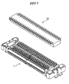
FIG. 1 is a perspective view of a connector device according to an embodiment of the present invention, in a non-fitted state; -
FIG. 2 is a side view of theFIG. 1 connector device in the non-fitted state; -
FIG. 3 is a perspective view of theFIG. 1 connector device in a fitted state; -
FIG. 4 is a side view of theFIG. 1 connector device in the fitted state; -
FIG. 5 is a perspective view of a receptacle connector of theFIG. 1 connector device; -
FIG. 6 is a perspective view of one end of theFIG. 5 receptacle connector; -
FIG. 7 is a perspective view of a central portion of theFIG. 5 receptacle connector; -
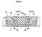
FIG. 8 is a cross-sectional view of one end of theFIG. 3 connector device; -
FIG. 9 is a perspective view of theFIG. 3 connector device, in a state cross-sectioned at a central portion thereof; -
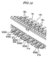
FIG. 10 is a perspective view of the central portion of theFIG. 3 connector device; -
FIG. 11 is a perspective view of a shell of theFIG. 5 receptacle connector; -
FIG. 12 is a perspective view of a plug connector of the connector device shown inFIG. 1 , in a state presented in an inverted position; -
FIG. 13 is a perspective view of one end of theFIG. 12 plug connector; -
FIG. 14 is a side view of a plug-side contact of theFIG. 12 plug connector; and -
FIG. 15 is a perspective view of theFIG. 14 plug-side contact. - The present invention will now be described in detail with reference to the drawings showing a preferred embodiment thereof.
- Referring to
FIGS. 1 to 4 , theconnector device 100 is comprised of the receptacle connector (connector) 1 and a plug connector (mating connector) 12, Thereceptacle connector 1 is mounted on a first printed circuit board (circuit board) 21 (seeFIG. 9 ) and theplug connector 12 is mounted on a second printed circuit board (mating circuit board), not shown. - As shown in
FIG. 5 , thereceptacle connector 1 includes a receptacle-side housing (housing) 3, receptacle-side contacts (contacts) 5, and theshell 7. - As shown in
FIGS. 6 to 8 , the receptacle-side housing 3 includes a plate-like portion 31 and a receptacle-side fitting portion (fitting portion) 32. - The plate-
like portion 31 is disposed on the first printedcircuit board 21. The plate-like portion 31 is slightly lifted from the first printedcircuit board 21. - The receptacle-side
fitting portion 32 is formed on an upper surface of the plate-like portion 31. The receptacle-sidefitting portion 32 is comprised of a frame-like portion 32a and acentral protrusion 32b. The frame-like portion 32a has a pair ofside wall portions ends side wall portions side wall portion 32c is formed with a plurality ofgrooves 32e at predetermined spaced intervals. The pair ofends side wall portions - The
central protrusion 32b is disposed in parallel with the pair ofside wall portions central protrusion 32b is formed with a plurality ofgrooves 32f at the same spaced intervals as those of the plurality ofgrooves 32e. Thegrooves 32f are opposed to thegrooves 32e, respectively. Thecentral protrusion 32b is surrounded by the frame-like portion 32a. A receivingspace 32g is formed between the frame-like portion 32a and thecentral protrusion 32b. The receptacle-sidefitting portion 32 receives a plug-sidefitting portion 142 of a plug-side housing, described hereinafter. - As shown in
FIGS. 9 and10 , each receptacle-side contact 5 includes afirst contact portion 5a, asecond contact portion 5b, a heldportion 5c, and aterminal portion 5d. Thefirst contact portion 5a is formed at the intermediate portion of the receptacle-side contact 5. Thesecond contact portion 5b is substantially e-shaped, and is connected to one end of thefirst contact portion 5a. Thesecond contact portion 5b is elastically deformably received in eachgroove 32f. The heldportion 5c is substantially inverted L-shaped, and is connected to the other end of thefirst contact portion 5a. The heldportion 5c is received in eachgroove 32e to be held therein. Theterminal portion 5d is substantially I-shaped, and is connected to the heldportion 5c. The lower surface of theterminal portion 5d is located below the lower surface of the plate-like portion 31. Thefirst contact portion 5a is in contact with a plug-sidefirst contact portion 16a, and thesecond contact portion 5b is in contact with a plug-sidesecond contact portion 16b and is connected to the same. Further, thefirst contact portion 5a is improved in a force in a direction of withdrawal of the connector, by a steppedportion 16e (seeFIG. 14 ) of the plug-sidefirst contact portion 16a, which increases a withdrawing force. - The receptacle-
side contacts 5 include two kinds of contacts, i.e. receptacle-side signal contacts 5S and receptacle-side ground contacts (ground contacts) 5G. The shapes, sizes and materials of thecontacts side signal contact 5S is formed by soldering theterminal portion 5d to asignal pad 21a of the printedcircuit board 21, while the receptacle-side ground contact 5G is formed by soldering theterminal portion 5d to a ground pad (second ground trace) 21b of the first printedcircuit board 21. However, the arrangement of thesignal contacts 5S and the receptacle-side ground contacts 5G on the receptacle-side housing 3 is determined in advance, and thesignal pads 21a and theground pad 21b of the first printedcircuit board 21 are formed in a manner associated with the arrangedcontacts - Further, the plurality of the receptacle-
side contacts 5 are grouped into four contact groups A, B, C, and D, with thecentral protrusion 32b and two secondshell terminal portions 74 of theshell 7, described hereinafter, as boundaries (seeFIG. 5 ). - Referring to
FIG. 11 , the shell 7is comprised of ashell body 71,shell contact portions 72, first shell terminal portions (shell terminal portions) 73, the second shell terminal portions (auxiliary shell terminal portions) 74, fixedly engagingportions 75, and hold-down and shellterminal portions 76. - The
shell body 71 is substantially frame-like, and includes a pair ofside plates end plates side plates side wall portions fitting portion 32. The pair ofend plates side plates end plates 71b cover the respective outer surfaces of theends 32d of the receptacle-sidefitting portion 32. - The
shell contact portions 72 are connected to the upper edges of the opposite ends of theside plates 71a. Eachshell contact portion 72 protrudes inward from theside plate 71a. Theshell contact portion 72 is bent into a substantially U-shape, and is generally T-shaped in developed plan view. Theshell contact portion 72 has a foremost end formed with twocontact points 72a. The distance between the twocontact points 72a is equal to the distance between plug-side ground contacts 16G (seeFIGS. 6 and13 ). The twocontact points 72a are brought into contact with two of the plug-side ground contacts 16G, described hereinafter, respectively. - The first
shell terminal portions 73 are connected to the lower edges of the ends of theside plates 71a. Each firstshell terminal portion 73 protrudes outward from theside plate 71a. The firstshell terminal portion 73 is soldered to a ground pad (first ground trace), not shown, of the first printedcircuit board 21. The firstshell terminal portion 73 has a large width, and hence it is possible to enhance a soldering strength. - The second
shell terminal portions 74 are connected to the lower edges of the central portions of theside plates 71a. Each secondshell terminal portion 74 protrudes outward from theside plate 71a. The secondshell terminal portion 74 is disposed between two receptacle-side ground contacts 5G, and is soldered to theground pad 21b of the first printedcircuit board 21. The secondshell terminal portion 74 is located at the intermediate portion of eachside plate 71a, so that the rigidity of theshell 7 is enhanced by the soldering of the secondshell terminal portion 74 to the ground pad. - The fixedly engaging
portions 75 are connected to the upper edges of the central portions of theside plates 71a. Each fixedly engagingportion 75 protrudes inward from theside plate 71a. Thefixedly engaging portion 75 is bent into a substantially U-shape. Thefixedly engaging portion 75 is disposed between the two receptacle-side ground contacts 5G (seeFIG. 9 ). Thefixedly engaging portion 75 is engaged with an engagingportion 32h (seeFIG. 9 ) formed on an associated one of theside wall portions 32c of the receptacle-side housing 3. Theside plates 71a are in contact with the respectiveside wall portions 32c. - The pair of
end plates 71b each have the two hold-down and shellterminal portions 76 connected to a lower edge thereof. Each hold-down and shellterminal portion 76 protrudes outward from theend plate 71b. The hold-down and shellterminal portion 76 is soldered to the ground pad of the first printedcircuit board 21. This causes thereceptacle connector 1 to be positively shielded by theshell 7, and be rigidly fixed to the first printedcircuit board 21. - The pair of
end plates 71b each have an upper edge formed with two holdingportions 77. Each holdingportion 77 is bent into a substantially U-shape. The holdingportion 77 is held by being press-fitted into an associated one of theends 32d of the receptacle-side fitting portion 3 (seeFIG. 6 ). It should be noted that the holdingportions 77 may be held by being integrally formed with the receptacle-side housing 3 during insert molding of thehousing 3. - As shown in
FIGS. 12 and13 , theplug connector 12 is comprised of a plug-side housing (mating housing) 14 and a plurality of plug-side contacts (mating contacts) 16. - The plug-
side housing 14 includes a plate-like portion 141 and a plug-side fitting portion (mating fitting portion) 142. - The plate-
like portion 141 is disposed on a second printed circuit board, not shown. The plate-like portion 141 is slightly lifted from the second printed circuit board. - The plug-side
fitting portion 142 is formed on a lower surface of the plate-like portion 141. The plug-sidefitting portion 142 has a frame-like shape. The plug-sidefitting portion 142 has a pair ofside wall portions 142a and a pair ofends 142b. The pair ofside wall portions 142a are arranged in parallel with each other, and eachside wall portion 142a is formed with a plurality ofgrooves 142c at predetermined spaced intervals. The pair ofends side wall portions - As shown in
FIGS. 14 and15 , each plug-side contact 16 includes a first contact portion (mating shell contact portion) 16a, asecond contact portion 16b, a terminal portion (mating terminal portion) 16c, and an embeddedportion 16d. Thefirst contact portion 16a is formed in the vicinity of the foremost end of the plug-side contact 16. Thefirst contact portion 16a is in contact with an associated one of thefirst contact portions 5a of the receptacle-side contacts 5. Thesecond contact portion 16b is connected to one end of thefirst contact portion 16a. Thesecond contact portion 16b is in contact with an associated one of thesecond contact portions 5b of the receptacle-side contacts 5. Thefirst contact portion 16a and thesecond contact portion 16b enclose an associated one of theside wall portions 142a (seeFIG. 9 ). Theterminal portion 16c is generally crank-shaped, and is connected to thesecond contact portion 16b. The upper surface of theterminal portion 16c is located above the upper surface of the plate-like portion 141 (seeFIG. 10 ). The embeddedportion 16d is connected to the other end of thefirst contact portion 16a. The embeddedportion 16d is embedded during insert molding of the plug-side housing 14. Although in the present embodiment, the plug-side housing 14 and the plug-side contact 16 are integrally formed with each other, the foremost end of thefirst contact portion 16a may be press-fitted into the plug-side housing 14 to hold the plug-side contact 16, by removing the embeddedportion 16d. - Although the plug-
side contacts 16 include two kinds of contacts, i.e. plug-side signal contacts 16S and plug-side ground contacts (mating ground contacts) 16G, the shapes, sizes and materials of thecontacts side signal contact 16S is formed by soldering theterminal portion 16c to a signal pad of the second printed circuit board, while the plug-side ground contact 16G is formed by soldering theterminal portion 16c to a ground pad (ground trace) of the second printed circuit board. However, the arrangement of the plug-side signal contacts 16S and the plug-side ground contacts 16G on the plug-side housing 14 is determined in advance, and the signal pads and the ground pad of the second printed circuit board are formed in a manner associated with the arrangedcontacts - The plug-
side signal contacts 16S each have thefirst contact portion 16 and thesecond contact portion 16b exposed, whereas as to the plug-side ground contacts 16G, only the four plug-side ground contacts 16G arranged on opposite ends of theplug connector 12 each have only thefirst contact portion 16a exposed, with thesecond contact portion 16b embedded in anend 142b of the plug-side housing 14 together with the embeddedportion 16d. - The
plug connector 12 is disposed above the receptacle connector 1 (seeFIGS. 1 and2 ), and from this state, when theplug connector 12 is lowered, as indicated by an arrow inFIG. 2 , to push the plug-sidefitting portion 142 of theplug connector 12 into the receptacle-sidefitting portion 32 of thereceptacle connector 1, thereceptacle connector 1 and theplug connector 12 are fitted to each other (seeFIGS. 3 and4 ). As a result, the first and second printed circuit boards are electrically connected to each other via theconnectors - At this time, the plug-side
fitting portion 142 of theplug connector 12 is received in the receptacle-sidefitting portion 32 of thereceptacle connector 1, and the plug-side ground contacts 16G of theplug connector 12 are brought into contact with theshell contact portions 72 of theshell 7 of thereceptacle connector 1, so that the ground pad of the first printedcircuit board 21 on which is mounted thereceptacle connector 1, and the ground pad of the second printed circuit board on which is mounted theplug connector 12 are connected to each other. Further, when theconnectors fitting portion 142 of theplug connector 12 is surrounded by theshell body 71 of theshell 7 of thereceptacle connector 1. This makes it possible to obtain more stable grounding effects. - According to the present embodiment, since the shell can be removed from the
plug connector 12, it is possible to reduce the size of theplug connector 12. - Further, since the
receptacle connector 1 includes the hold-down and shellterminal portions 76, it is possible to mount thereceptacle connector 1 on the first printedcircuit board 21 more positively and shield theconnectors - Further, the second
shell terminal portion 74 is located at the intermediate portion of thereceptacle connector 1, and located between the two adjacent contact groups, which makes it possible to realize further enhancement of the ground. It should be noted that although one secondshell terminal portion 74 and one fixedly engagingportion 75 are arranged on one and the other of each pair ofside plates 71a, respectively, a plurality of secondshell terminal portions 74 and a plurality of fixedly engagingportions 75 may be arranged on one and the other of each pair ofside plates 71a. - It should be noted that although in the present embodiment, the
shell 7 has the secondshell terminal portions 74, the fixedly engagingportions 75, the hold-down and shellterminal portions 76, and the holdingportions 77, it is possible to omit them. - Further, although the four
shell contact portions 72 and the fourshell terminal portions 73 are provided in theshell 7, the number of theshell contact portions 72 and that ofshell terminal portions 73 are not particularly limited. - It is further understood by those skilled in the art that the foregoing are the preferred embodiments of the present invention, and that various changes and modification may be made thereto without departing from the spirit and scope thereof. The invention includes within its scope in particular the following embodiments:
- A. A connector for use with a further, mating connector in electrically connecting first and second circuit boards one to the other, said connector including housing that has a fitting portion for being fitted to a mating fitting portion of the mating connector, said connector for disposition on the first circuit board, a plurality of contacts that are arranged in said fitting portion, and a shell that has a shell body disposed around said fitting portion and is mounted on said housing,
characterized in that
said shell has a shell contact portion to be brought into contact with a mating ground contact of said mating connector, and a shell terminal portion fixed to a first ground trace of said first circuit board. - B. A mating connector for use with a further connector to which it is matable in connecting first and second circuit boards electrically one to another, said mating connector including a mating housing that has a mating fitting portion for fitting to a fitting portion of the further connector, said mating connector for disposition on the second of said circuit boards, with said further connector for disposition on the first of said circuit boards, and a plurality of mating contacts that are arranged in said mating fitting portion,
said plurality of mating contacts include a mating ground contact, and
said mating ground contact having a mating shell contact portion brought into contact with a shell mounted in a housing of said mating connector, and a mating terminal portion fixed to a ground trace of said second circuit board.
Claims (3)
- A connector including housing that has a fitting portion for being fitted to a mating fitting portion of a mating connector, and is disposed on a circuit board, a plurality of contacts that are arranged in said fitting portion, and a shell that has a shell body disposed around said fitting portion and is mounted on said housing,
characterized in that
said shell has a shell contact portion brought into contact with a mating ground contact of said mating connector, and a shell terminal portion fixed to a first ground trace of said circuit board. - A connector as claimed in claim 1, wherein said plurality of contacts include at least one ground contact, and
wherein said shell has a fixedly engaging portion that is connected to said shell body, and causes said shell body to be fixedly engaged with said housing, and an auxiliary shell terminal portion adjacent to said one ground contact, said auxiliary shell terminal portion being connected to said shell body and fixed to a second ground trace. - A mating connector including a mating housing that has a mating fitting portion for being fitted to a fitting portion of a connector, and is disposed on a mating circuit board, and a plurality of mating contacts that are arranged in said mating fitting portion,
characterized in that
said plurality of mating contacts including a mating ground contact, and
said mating ground contact having a mating shell contact portion brought into contact with a shell mounted in a housing of said connector, and a mating terminal portion fixed to a ground trace of said mating circuit board.
Applications Claiming Priority (1)
| Application Number | Priority Date | Filing Date | Title |
|---|---|---|---|
| JP2007051561A JP4333884B2 (en) | 2007-03-01 | 2007-03-01 | connector |
Publications (3)
| Publication Number | Publication Date |
|---|---|
| EP1965466A2 true EP1965466A2 (en) | 2008-09-03 |
| EP1965466A3 EP1965466A3 (en) | 2009-10-21 |
| EP1965466B1 EP1965466B1 (en) | 2015-07-08 |
Family
ID=39473612
Family Applications (1)
| Application Number | Title | Priority Date | Filing Date |
|---|---|---|---|
| EP08003354.1A Ceased EP1965466B1 (en) | 2007-03-01 | 2008-02-25 | Connector |
Country Status (6)
| Country | Link |
|---|---|
| US (1) | US7585185B2 (en) |
| EP (1) | EP1965466B1 (en) |
| JP (1) | JP4333884B2 (en) |
| KR (1) | KR100993049B1 (en) |
| CN (1) | CN101257169B (en) |
| TW (1) | TWI381595B (en) |
Cited By (2)
| Publication number | Priority date | Publication date | Assignee | Title |
|---|---|---|---|---|
| EP2763244A1 (en) * | 2013-02-05 | 2014-08-06 | Tyco Electronics Japan G.K. | Electrical connector assembly and electrical connector used therefor |
| EP3451465A4 (en) * | 2016-04-28 | 2019-04-24 | Panasonic Intellectual Property Management Co., Ltd. | Mounting fitting, connector, and connection system |
Families Citing this family (89)
| Publication number | Priority date | Publication date | Assignee | Title |
|---|---|---|---|---|
| USD609648S1 (en) | 2008-11-14 | 2010-02-09 | Japan Aviation Electronics Industry, Limited | Electrical connector |
| USD609649S1 (en) | 2008-11-20 | 2010-02-09 | Japan Aviation Electronics Industry, Limited | Electrical connector |
| JP5250450B2 (en) * | 2009-02-27 | 2013-07-31 | 第一電子工業株式会社 | Electrical connector |
| KR101113525B1 (en) * | 2009-09-02 | 2012-02-29 | 엘에스엠트론 주식회사 | Connector unit with fastening guide |
| JP5586395B2 (en) * | 2010-09-21 | 2014-09-10 | モレックス インコーポレイテド | Board to board connector |
| JP2012089336A (en) | 2010-10-19 | 2012-05-10 | Panasonic Corp | Connector and socket used therefor |
| KR101078971B1 (en) | 2011-05-18 | 2011-11-01 | 엘에스엠트론 주식회사 | Connector device having coupling guide |
| JP5748334B2 (en) * | 2011-05-31 | 2015-07-15 | 日本航空電子工業株式会社 | Connectors and connector units |
| CN102810778B (en) * | 2011-06-03 | 2014-09-17 | 达昌电子科技(苏州)有限公司 | Connector |
| US8292630B1 (en) | 2011-06-24 | 2012-10-23 | Hon Hai Precision Inc. Co., Ltd. | Board mounted connector with protective shell |
| JP5890117B2 (en) * | 2011-07-07 | 2016-03-22 | 日本航空電子工業株式会社 | connector |
| JP5787081B2 (en) * | 2011-10-14 | 2015-09-30 | 第一精工株式会社 | Connector device |
| KR101355575B1 (en) | 2012-01-31 | 2014-01-24 | 엘에스엠트론 주식회사 | Improved connector device for shell structure |
| JP5638026B2 (en) * | 2012-05-01 | 2014-12-10 | ヒロセ電機株式会社 | Electrical connector assembly |
| JP5818016B2 (en) * | 2012-05-17 | 2015-11-18 | 第一精工株式会社 | Connector device |
| US8888506B2 (en) * | 2013-01-29 | 2014-11-18 | Japan Aviation Electronics Industry, Limited | Connector |
| CN104137344B (en) * | 2013-02-27 | 2017-06-30 | 松下知识产权经营株式会社 | Connector, and plug and socket used in the connector |
| JP5809198B2 (en) * | 2013-06-10 | 2015-11-10 | ヒロセ電機株式会社 | Electrical connector with guide bracket |
| JP6249643B2 (en) | 2013-06-14 | 2017-12-20 | 宏致電子股▲ふん▼有限公司Aces Electronics Co.,Ltd. | Electrical connector |
| JP5896959B2 (en) * | 2013-06-14 | 2016-03-30 | ヒロセ電機株式会社 | Circuit board electrical connector and electrical connector assembly |
| JP5747953B2 (en) * | 2013-06-27 | 2015-07-15 | Smk株式会社 | connector |
| KR101488892B1 (en) * | 2013-08-08 | 2015-02-02 | 엘에스엠트론 주식회사 | Connector assembly for board-to-board |
| KR101496720B1 (en) * | 2013-11-08 | 2015-02-27 | (주)우주일렉트로닉스 | Shield and locking type board to board connector |
| JP5881666B2 (en) * | 2013-11-19 | 2016-03-09 | 京セラコネクタプロダクツ株式会社 | Manufacturing method of receptacle connector |
| US9065228B2 (en) * | 2013-11-21 | 2015-06-23 | Japan Aviation Electronics Industry, Limited | Connector |
| JP6245964B2 (en) * | 2013-12-02 | 2017-12-13 | モレックス エルエルシー | connector |
| JP5887326B2 (en) | 2013-12-12 | 2016-03-16 | モレックス エルエルシー | connector |
| JP5972855B2 (en) * | 2013-12-24 | 2016-08-17 | ヒロセ電機株式会社 | Electrical connector |
| JP6291257B2 (en) * | 2014-01-06 | 2018-03-14 | モレックス エルエルシー | connector |
| US9300064B2 (en) * | 2014-01-17 | 2016-03-29 | Japan Aviation Electronics Industry, Limited | Connector |
| JP6325262B2 (en) * | 2014-01-29 | 2018-05-16 | 日本航空電子工業株式会社 | connector |
| JP6167997B2 (en) * | 2014-06-05 | 2017-07-26 | 株式会社村田製作所 | Connector set and connector |
| JP6327973B2 (en) * | 2014-06-30 | 2018-05-23 | モレックス エルエルシー | connector |
| CN105305165B (en) * | 2014-07-16 | 2018-10-02 | 广濑电机株式会社 | Circuit board electric connector |
| JP6051242B2 (en) * | 2014-07-16 | 2016-12-27 | ヒロセ電機株式会社 | Circuit board electrical connector |
| JP6034339B2 (en) * | 2014-07-29 | 2016-11-30 | ヒロセ電機株式会社 | Circuit board electrical connector |
| JP6537890B2 (en) * | 2014-09-26 | 2019-07-03 | 日本航空電子工業株式会社 | connector |
| CN112086780B (en) | 2014-10-23 | 2022-11-01 | 安费诺富加宜(亚洲)私人有限公司 | Sandwich type electric connector |
| US9401570B2 (en) * | 2014-10-29 | 2016-07-26 | Tyco Electronics Corporation | Electrical connector having ground bus bar |
| JP6052268B2 (en) * | 2014-11-28 | 2016-12-27 | 第一精工株式会社 | Electrical connector and electrical connector device |
| US9692183B2 (en) * | 2015-01-20 | 2017-06-27 | Te Connectivity Corporation | Receptacle connector with ground bus |
| JP6436350B2 (en) | 2015-03-18 | 2018-12-12 | 第一精工株式会社 | Connector device |
| JP6378642B2 (en) | 2015-04-23 | 2018-08-22 | モレックス エルエルシー | connector |
| KR102325309B1 (en) * | 2015-05-22 | 2021-11-11 | 삼성전자주식회사 | Electronic device including conncetor |
| JP6513509B2 (en) * | 2015-07-01 | 2019-05-15 | 日本航空電子工業株式会社 | Board to Board Connectors and Connectors |
| JP6179564B2 (en) | 2015-07-29 | 2017-08-16 | 第一精工株式会社 | Electrical connector for board connection |
| US10084265B2 (en) | 2015-07-29 | 2018-09-25 | Dai-Ichi Seiko Co., Ltd. | Board-connecting electric connector device |
| JP6281539B2 (en) * | 2015-07-29 | 2018-02-21 | 第一精工株式会社 | Electric connector device for board connection |
| JP6256426B2 (en) | 2015-07-29 | 2018-01-10 | 第一精工株式会社 | Electrical connector for board connection |
| US9893480B2 (en) * | 2015-09-04 | 2018-02-13 | Tyco Electronics Japan G.K. | Connector |
| KR20170036529A (en) * | 2015-09-24 | 2017-04-03 | 몰렉스 엘엘씨 | Board to board connector and rf connector integral connector assembly |
| TWM517433U (en) * | 2015-11-24 | 2016-02-11 | 正崴精密工業股份有限公司 | Electrical connector and its terminal |
| US9831579B1 (en) * | 2016-08-01 | 2017-11-28 | Motorola Solutions, Inc. | Adapter frame with a set of electrical pads on its top and bottom surfaces for a board-to-board connection |
| JP6885730B2 (en) * | 2017-01-06 | 2021-06-16 | ヒロセ電機株式会社 | Connector with shielding shield plate |
| JP6806028B2 (en) * | 2017-01-19 | 2020-12-23 | 株式会社村田製作所 | Multi-pole connector set |
| US10404014B2 (en) * | 2017-02-17 | 2019-09-03 | Fci Usa Llc | Stacking electrical connector with reduced crosstalk |
| CN113193402B (en) | 2017-04-28 | 2023-06-02 | 富加宜(美国)有限责任公司 | High frequency BGA connector |
| JP6573135B2 (en) * | 2017-11-06 | 2019-09-11 | 第一精工株式会社 | Electrical connector device |
| CN110021835A (en) * | 2018-01-09 | 2019-07-16 | 岱炜科技股份有限公司 | The composite structure of connector |
| CN110021836A (en) * | 2018-01-09 | 2019-07-16 | 岱炜科技股份有限公司 | The structure of bus bar connector |
| JP6563046B2 (en) * | 2018-02-08 | 2019-08-21 | モレックス エルエルシー | connector |
| KR102041368B1 (en) | 2018-05-24 | 2019-11-07 | 몰렉스 엘엘씨 | Receptacle connector and connector assembly including the same |
| JP7093273B2 (en) * | 2018-09-07 | 2022-06-29 | 日本航空電子工業株式会社 | connector |
| US10594074B1 (en) * | 2018-10-30 | 2020-03-17 | Microsoft Technology Licensing, Llc | Shielded magnetic electronic connector |
| JP6643641B2 (en) * | 2018-11-13 | 2020-02-12 | パナソニックIpマネジメント株式会社 | Connector, socket and connection structure between socket and circuit board |
| JP7202937B2 (en) * | 2018-12-19 | 2023-01-12 | モレックス エルエルシー | Connectors and connector assemblies |
| JP7108531B2 (en) * | 2018-12-27 | 2022-07-28 | モレックス エルエルシー | connector assembly |
| CN209329318U (en) * | 2018-12-28 | 2019-08-30 | 富士康(昆山)电脑接插件有限公司 | Electric connector and its docking connector |
| JP7245052B2 (en) * | 2019-01-07 | 2023-03-23 | ヒロセ電機株式会社 | Connectors and connector devices |
| JP7184157B2 (en) * | 2019-02-27 | 2022-12-06 | 株式会社村田製作所 | connector, connector set |
| JP7411882B2 (en) * | 2019-08-08 | 2024-01-12 | パナソニックIpマネジメント株式会社 | connector |
| JP7120469B2 (en) * | 2019-09-24 | 2022-08-17 | 株式会社村田製作所 | Electrical connectors and electrical connector sets |
| JP7244412B2 (en) * | 2019-12-25 | 2023-03-22 | 京セラ株式会社 | Connectors and electronics |
| KR102842594B1 (en) * | 2020-02-06 | 2025-08-06 | 삼성전자주식회사 | An electronic device and a connector connecting the first printed circuit board and the second printed circuit board of the electronic device |
| WO2021162357A1 (en) * | 2020-02-14 | 2021-08-19 | 엘에스엠트론 주식회사 | Board connector |
| TWI900541B (en) * | 2020-03-10 | 2025-10-11 | 日商宏致日本股份有限公司 | Contacts, connectors and lighting devices |
| JP7454995B2 (en) * | 2020-05-11 | 2024-03-25 | モレックス エルエルシー | Connectors and connector pairs |
| US11495919B2 (en) * | 2020-05-13 | 2022-11-08 | Japan Aviation Electronics Industry, Limited | Connector assembly in which ground terminals are coupled to form a shielding |
| KR102494901B1 (en) * | 2020-05-13 | 2023-02-06 | 니혼 고꾸 덴시 고교 가부시끼가이샤 | Connector assembly and connector |
| US11489291B2 (en) * | 2020-05-13 | 2022-11-01 | Japan Aviation Electronics Industry, Limited | Board-to-board connector and connector assembly |
| US11652323B2 (en) * | 2020-05-13 | 2023-05-16 | Japan Aviation Electronics Industry, Limited | Connector assembly comprising a connector encolsed by a shell and a mating connector enclosed by a mating shell |
| JP7467234B2 (en) * | 2020-05-28 | 2024-04-15 | 日本航空電子工業株式会社 | Floating Connector |
| JP7592424B2 (en) * | 2020-08-03 | 2024-12-02 | ヒロセ電機株式会社 | Board to Board Connector |
| JP7485988B2 (en) * | 2020-08-31 | 2024-05-17 | 山一電機株式会社 | connector |
| CN114498200B (en) * | 2020-10-23 | 2024-01-16 | 富士康(昆山)电脑接插件有限公司 | Electric connector |
| US11757223B2 (en) * | 2021-04-14 | 2023-09-12 | Dell Products L.P. | Receptacle connector socket with embedded bus bar |
| CN217182551U (en) * | 2021-05-17 | 2022-08-12 | 日本航空电子工业株式会社 | Connector and connector assembly |
| JP7862238B2 (en) * | 2022-06-16 | 2026-05-19 | モレックス エルエルシー | Connectors and connector pairs |
| JP7881417B2 (en) * | 2022-08-29 | 2026-06-29 | 日本航空電子工業株式会社 | connector |
Citations (1)
| Publication number | Priority date | Publication date | Assignee | Title |
|---|---|---|---|---|
| JPH11233201A (en) | 1998-02-16 | 1999-08-27 | Hirose Electric Co Ltd | Electrical connector having a shield plate |
Family Cites Families (9)
| Publication number | Priority date | Publication date | Assignee | Title |
|---|---|---|---|---|
| CN1096127C (en) * | 1995-02-09 | 2002-12-11 | 惠特克公司 | Electrical connector for printed circuit boards |
| US6019616A (en) * | 1996-03-01 | 2000-02-01 | Molex Incorporated | Electrical connector with enhanced grounding characteristics |
| JPH09237655A (en) * | 1996-03-01 | 1997-09-09 | Molex Inc | Ground-reinforced electrical connector assembly |
| JP3882958B2 (en) * | 1997-06-30 | 2007-02-21 | タイコエレクトロニクスアンプ株式会社 | Movable connector |
| JP3277154B2 (en) * | 1998-05-06 | 2002-04-22 | ケル株式会社 | connector |
| US6503101B1 (en) * | 2001-12-04 | 2003-01-07 | Hon Hai Precision Ind. Co., Ltd. | Electrical connector having grounding path |
| CN2667690Y (en) * | 2003-09-06 | 2004-12-29 | 富士康(昆山)电脑接插件有限公司 | Electric connector |
| JP4522144B2 (en) * | 2004-05-21 | 2010-08-11 | 日本航空電子工業株式会社 | Electrical connector |
| JP4758104B2 (en) * | 2005-01-21 | 2011-08-24 | 日本圧着端子製造株式会社 | Connector assembly |
-
2007
- 2007-03-01 JP JP2007051561A patent/JP4333884B2/en active Active
-
2008
- 2008-02-22 TW TW097106350A patent/TWI381595B/en not_active IP Right Cessation
- 2008-02-25 EP EP08003354.1A patent/EP1965466B1/en not_active Ceased
- 2008-02-27 KR KR1020080017642A patent/KR100993049B1/en not_active Expired - Fee Related
- 2008-02-27 US US12/072,705 patent/US7585185B2/en not_active Expired - Fee Related
- 2008-02-29 CN CN200810082266XA patent/CN101257169B/en not_active Expired - Fee Related
Patent Citations (1)
| Publication number | Priority date | Publication date | Assignee | Title |
|---|---|---|---|---|
| JPH11233201A (en) | 1998-02-16 | 1999-08-27 | Hirose Electric Co Ltd | Electrical connector having a shield plate |
Cited By (6)
| Publication number | Priority date | Publication date | Assignee | Title |
|---|---|---|---|---|
| EP2763244A1 (en) * | 2013-02-05 | 2014-08-06 | Tyco Electronics Japan G.K. | Electrical connector assembly and electrical connector used therefor |
| CN103972748A (en) * | 2013-02-05 | 2014-08-06 | 泰科电子日本合同会社 | Electrical connector assembly and electrical connector for the same |
| US9203172B2 (en) | 2013-02-05 | 2015-12-01 | Tyco Electronics Japan G.K. | Electrical connector assembly and electrical connector used therefor |
| EP3451465A4 (en) * | 2016-04-28 | 2019-04-24 | Panasonic Intellectual Property Management Co., Ltd. | Mounting fitting, connector, and connection system |
| US10498056B2 (en) | 2016-04-28 | 2019-12-03 | Panasonic Intellectual Property Management Co., Ltd. | Mounting metal fitting, connector and connection system |
| US10998655B2 (en) | 2016-04-28 | 2021-05-04 | Panasonic Intellectual Property Management Co., Ltd. | Connector and connection system |
Also Published As
| Publication number | Publication date |
|---|---|
| TWI381595B (en) | 2013-01-01 |
| US20080214051A1 (en) | 2008-09-04 |
| KR20080080435A (en) | 2008-09-04 |
| JP4333884B2 (en) | 2009-09-16 |
| US7585185B2 (en) | 2009-09-08 |
| EP1965466B1 (en) | 2015-07-08 |
| CN101257169A (en) | 2008-09-03 |
| JP2008218095A (en) | 2008-09-18 |
| KR100993049B1 (en) | 2010-11-08 |
| TW200843247A (en) | 2008-11-01 |
| CN101257169B (en) | 2010-09-29 |
| EP1965466A3 (en) | 2009-10-21 |
Similar Documents
| Publication | Publication Date | Title |
|---|---|---|
| US7585185B2 (en) | Connector | |
| US7922534B2 (en) | Socket connector | |
| EP2228871B1 (en) | EMI shielded connector mounted on a PCB | |
| CN103427238B (en) | Electrical connector | |
| US6908345B2 (en) | Electric connector and socket connector | |
| US6238240B1 (en) | PC card connector assembly | |
| CN2599815Y (en) | Electric connector | |
| US12149015B2 (en) | Connector | |
| US8062041B2 (en) | Connector | |
| EP0755098A2 (en) | IC card connector shield grounding | |
| JP7653557B2 (en) | Movable connector and shield manufacturing method | |
| US8070528B2 (en) | Electrical connector having improved terminals | |
| WO2006081439A1 (en) | Board mounted electrical connector | |
| US6022245A (en) | Filtered modular connector | |
| US7052286B2 (en) | Electrical connector with cover | |
| EP3316406B1 (en) | Electronic device and connector | |
| US20130178077A1 (en) | Connectors | |
| JP7176659B2 (en) | electrical connector | |
| US6743047B2 (en) | Electrical connector with rear ground plate | |
| US7625240B2 (en) | Receptacle connector | |
| JP5787081B2 (en) | Connector device | |
| CN116805772A (en) | Connector assembly and first connector | |
| CN2682662Y (en) | Electric connector | |
| US6027348A (en) | Grounding plate for an IC card connector apparatus | |
| TW201027848A (en) | Electrical connector |
Legal Events
| Date | Code | Title | Description |
|---|---|---|---|
| PUAI | Public reference made under article 153(3) epc to a published international application that has entered the european phase |
Free format text: ORIGINAL CODE: 0009012 |
|
| 17P | Request for examination filed |
Effective date: 20080320 |
|
| AK | Designated contracting states |
Kind code of ref document: A2 Designated state(s): AT BE BG CH CY CZ DE DK EE ES FI FR GB GR HR HU IE IS IT LI LT LU LV MC MT NL NO PL PT RO SE SI SK TR |
|
| AX | Request for extension of the european patent |
Extension state: AL BA MK RS |
|
| PUAL | Search report despatched |
Free format text: ORIGINAL CODE: 0009013 |
|
| AK | Designated contracting states |
Kind code of ref document: A3 Designated state(s): AT BE BG CH CY CZ DE DK EE ES FI FR GB GR HR HU IE IS IT LI LT LU LV MC MT NL NO PL PT RO SE SI SK TR |
|
| AX | Request for extension of the european patent |
Extension state: AL BA MK RS |
|
| 17Q | First examination report despatched |
Effective date: 20100318 |
|
| AKX | Designation fees paid |
Designated state(s): DE FI GB |
|
| REG | Reference to a national code |
Ref country code: DE Ref legal event code: R079 Ref document number: 602008038856 Country of ref document: DE Free format text: PREVIOUS MAIN CLASS: H01R0012040000 Ipc: H01R0012520000 |
|
| GRAP | Despatch of communication of intention to grant a patent |
Free format text: ORIGINAL CODE: EPIDOSNIGR1 |
|
| RIC1 | Information provided on ipc code assigned before grant |
Ipc: H01R 12/57 20110101ALI20150312BHEP Ipc: H01R 12/52 20110101AFI20150312BHEP Ipc: H01R 12/70 20110101ALI20150312BHEP Ipc: H01R 13/658 20110101ALI20150312BHEP Ipc: H01R 12/71 20110101ALI20150312BHEP |
|
| INTG | Intention to grant announced |
Effective date: 20150407 |
|
| GRAS | Grant fee paid |
Free format text: ORIGINAL CODE: EPIDOSNIGR3 |
|
| GRAA | (expected) grant |
Free format text: ORIGINAL CODE: 0009210 |
|
| AK | Designated contracting states |
Kind code of ref document: B1 Designated state(s): DE FI GB |
|
| REG | Reference to a national code |
Ref country code: GB Ref legal event code: FG4D |
|
| REG | Reference to a national code |
Ref country code: DE Ref legal event code: R096 Ref document number: 602008038856 Country of ref document: DE |
|
| REG | Reference to a national code |
Ref country code: DE Ref legal event code: R097 Ref document number: 602008038856 Country of ref document: DE |
|
| PLBE | No opposition filed within time limit |
Free format text: ORIGINAL CODE: 0009261 |
|
| STAA | Information on the status of an ep patent application or granted ep patent |
Free format text: STATUS: NO OPPOSITION FILED WITHIN TIME LIMIT |
|
| 26N | No opposition filed |
Effective date: 20160411 |
|
| PGFP | Annual fee paid to national office [announced via postgrant information from national office to epo] |
Ref country code: DE Payment date: 20170221 Year of fee payment: 10 |
|
| REG | Reference to a national code |
Ref country code: DE Ref legal event code: R119 Ref document number: 602008038856 Country of ref document: DE |
|
| PG25 | Lapsed in a contracting state [announced via postgrant information from national office to epo] |
Ref country code: DE Free format text: LAPSE BECAUSE OF NON-PAYMENT OF DUE FEES Effective date: 20180901 |
|
| PGFP | Annual fee paid to national office [announced via postgrant information from national office to epo] |
Ref country code: FI Payment date: 20210209 Year of fee payment: 14 |
|
| PGFP | Annual fee paid to national office [announced via postgrant information from national office to epo] |
Ref country code: GB Payment date: 20210217 Year of fee payment: 14 |
|
| REG | Reference to a national code |
Ref country code: FI Ref legal event code: MAE |
|
| GBPC | Gb: european patent ceased through non-payment of renewal fee |
Effective date: 20220225 |
|
| PG25 | Lapsed in a contracting state [announced via postgrant information from national office to epo] |
Ref country code: FI Free format text: LAPSE BECAUSE OF NON-PAYMENT OF DUE FEES Effective date: 20220225 |
|
| PG25 | Lapsed in a contracting state [announced via postgrant information from national office to epo] |
Ref country code: GB Free format text: LAPSE BECAUSE OF NON-PAYMENT OF DUE FEES Effective date: 20220225 |