EP1956658A2 - Ferroelectric infrared sensors and methods for their manufacturing - Google Patents
Ferroelectric infrared sensors and methods for their manufacturing Download PDFInfo
- Publication number
- EP1956658A2 EP1956658A2 EP08151080A EP08151080A EP1956658A2 EP 1956658 A2 EP1956658 A2 EP 1956658A2 EP 08151080 A EP08151080 A EP 08151080A EP 08151080 A EP08151080 A EP 08151080A EP 1956658 A2 EP1956658 A2 EP 1956658A2
- Authority
- EP
- European Patent Office
- Prior art keywords
- layer
- infrared
- platinum
- disposed
- depositing
- Prior art date
- Legal status (The legal status is an assumption and is not a legal conclusion. Google has not performed a legal analysis and makes no representation as to the accuracy of the status listed.)
- Withdrawn
Links
Images



Classifications
-
- H—ELECTRICITY
- H10—SEMICONDUCTOR DEVICES; ELECTRIC SOLID-STATE DEVICES NOT OTHERWISE PROVIDED FOR
- H10F—INORGANIC SEMICONDUCTOR DEVICES SENSITIVE TO INFRARED RADIATION, LIGHT, ELECTROMAGNETIC RADIATION OF SHORTER WAVELENGTH OR CORPUSCULAR RADIATION
- H10F30/00—Individual radiation-sensitive semiconductor devices in which radiation controls the flow of current through the devices, e.g. photodetectors
- H10F30/10—Individual radiation-sensitive semiconductor devices in which radiation controls the flow of current through the devices, e.g. photodetectors the devices being sensitive to infrared radiation, visible or ultraviolet radiation, and having no potential barriers, e.g. photoresistors
-
- H—ELECTRICITY
- H10—SEMICONDUCTOR DEVICES; ELECTRIC SOLID-STATE DEVICES NOT OTHERWISE PROVIDED FOR
- H10F—INORGANIC SEMICONDUCTOR DEVICES SENSITIVE TO INFRARED RADIATION, LIGHT, ELECTROMAGNETIC RADIATION OF SHORTER WAVELENGTH OR CORPUSCULAR RADIATION
- H10F71/00—Manufacture or treatment of devices covered by this subclass
-
- H—ELECTRICITY
- H10—SEMICONDUCTOR DEVICES; ELECTRIC SOLID-STATE DEVICES NOT OTHERWISE PROVIDED FOR
- H10F—INORGANIC SEMICONDUCTOR DEVICES SENSITIVE TO INFRARED RADIATION, LIGHT, ELECTROMAGNETIC RADIATION OF SHORTER WAVELENGTH OR CORPUSCULAR RADIATION
- H10F77/00—Constructional details of devices covered by this subclass
- H10F77/10—Semiconductor bodies
- H10F77/12—Active materials
Definitions
- This application relates to infrared sensors and methods for manufacturing the infrared sensors.
- Infrared sensors have been developed that detect infrared energy.
- a disadvantage associated with existing infrared sensors is that the sensors are not fabricated using integrated circuit "IC" compatible processes.
- manufacturers have not manufactured monolithic infrared sensors and peripheral ICs on the same chip.
- the inventors herein have recognized a need for an improved fabrication method for infrared sensors to overcome the above-identified shortcomings.
- a method for manufacturing an infrared sensor in accordance with an exemplary embodiment includes depositing an electrically insulative layer on a silicon substrate. The method further includes
- the method further includes depositing a germanium layer proximate to electrically insulative layer.
- the method further includes depositing a silicon nitride layer on a side of the germanium layer opposite the electrically insulative layer.
- the method further includes depositing a titanium layer on the silicon nitride layer.
- the method further includes disposing an infrared sensing structure on the titanium layer.
- the method further includes removing the germanium layer by applying a liquid on the germanium layer that dissolves the germanium layer such that a cavity is formed between the electrically insulative layer and the silicon nitride layer, the cavity configured to capture a portion of infrared energy therein that is received by the infrared sensing structure.
- the infrared sensor includes a silicon substrate.
- the infrared sensor further includes an electrically insulative layer disposed on the silicon substrate.
- the infrared sensor further includes a silicon nitride layer disposed proximate to the electrically insulative layer such that a cavity is formed therebetween.
- the infrared sensor further includes a titanium layer disposed on a side of the silicon nitride layer opposite the electrically insulative layer.
- the infrared sensor further includes an infrared sensing structure disposed on the titanium layer configured to generate a signal indicative of an amount of infrared energy being received by the infrared sensing structure.
- the cavity is configured to capture a portion of the infrared energy that is received by the infrared sensing structure.
- a method for manufacturing an infrared sensor in accordance with another exemplary embodiment includes depositing an electrically insulative layer on a silicon substrate. The method further includes depositing a germanium layer proximate to the electrically insulative layer. The method further includes depositing a titanium layer on the germanium layer. The method further includes disposing an infrared sensing structure on the titanium layer. The method further includes removing the germanium layer by applying a liquid on the germanium layer that dissolves the germanium layer such that a cavity is formed between the electrically insulative layer and the titanium layer. The cavity is configured to capture a portion of infrared energy therein that is received by the infrared sensing structure.
- the infrared sensor includes a silicon substrate.
- the infrared sensor further includes an electrically insulative layer disposed on the silicon substrate.
- the infrared sensor further includes a titanium layer disposed proximate to the electrically insulative layer such that a cavity is formed therebetween.
- the infrared sensor further includes an infrared sensing structure disposed on the titanium layer configured to generate a signal indicative of an amount of infrared energy being received by the infrared sensing structure.
- the cavity captures a portion of the infrared energy received by the infrared sensing structure therein.
- a method for manufacturing an infrared sensor in accordance with another exemplary embodiment includes depositing a germanium layer on a silicon substrate.
- the method further includes depositing a first electrically conductive layer on both the germanium layer and a portion of the silicon substrate.
- the method further includes depositing a ferroelectric layer on the first electrically conductive layer opposite the germanium layer.
- the method further includes depositing a second electrically conductive layer on both the ferroelectric layer and a portion of the silicon substrate.
- the method further includes removing the germanium layer by applying a liquid on the germanium layer that dissolves the germanium layer such that a cavity is formed between the first electrically conductive layer and the silicon substrate. The cavity is configured to capture a portion of infrared energy therein that is received by the first electrically conductive layer, the ferroelectric layer, and the second electrically conductive layer.
- the infrared sensor includes a silicon substrate.
- the infrared sensor further includes a first electrically conductive layer disposed on a portion of the silicon substrate such that a cavity is formed between a portion of the first electrically conductive layer and the silicon substrate.
- the infrared sensor further includes a ferroelectric layer disposed on the first electrically conductive layer opposite the cavity.
- the infrared sensor further includes a second electrically conductive layer disposed on both the ferroelectric layer and another portion of the silicon substrate.
- the first electrically conductive layer, the ferroelectric layer, and the second electrically conductive layer are configured to generate a signal indicative of an amount of infrared energy being received by the first electrically conductive layer, the ferroelectric layer, and the second electrically conductive layer.
- the cavity is configured to capture a portion of the infrared energy received by the first electrically conductive layer, the ferroelectric layer and the second electrically conductive layer.
- the manufacturing system 10 includes a plasma enhanced chemical vapor deposition machine 12, an evaporative deposition machine 14, a sol-gel deposition machine 16, a reactive sputter deposition machine 18, and a metallo-organic decomposition machine 19.
- the plasma enhanced chemical vapor deposition machine 12 is provided to deposit or form a layer of a particular chemical compound on another layer.
- the machine 12 can deposit an electrically insulative layer such as a low temperature oxide layer on another layer.
- the machine 12 can deposit a germanium layer, a silicon nitride layer, and an oxynitride layer, on another layer.
- the evaporative deposition machine 14 is provided to deposit or form a layer of a particular chemical compound on another layer.
- the machine 14 can deposit a titanium layer and a platinum layer on another layer.
- the sol-gel deposition machine 16 is provided to deposit or form a ferroelectric layer on another layer.
- the ferroelectric layer can comprise one of a strontium bismuth tantalate layer, a barium strontium titanate layer, a lead zirconate titanate layer, or the like, for example.
- the reactive sputter deposition machine 18 is provided to deposit or form a layer of a particular chemical compound on another layer.
- the machine 18 can deposit on another layer one or more of the following layers: a titanium layer, a platinum layer, and a chrome oxide layer.
- the metallo-organic decomposition machine 19 is provided to deposit or form a ferroelectric layer on another layer.
- the ferroelectric layer can comprise one of a strontium bismuth tantalate layer, a barium strontium titanate layer, a lead zirconate titanate layer, or the like, for example.
- the infrared sensor 30 includes a silicon substrate 32, an on-chip integrated circuit 34, an electrically insulative layer 36, a metal layer 38, a germanium layer 40, a silicon nitride layer 44, a titanium layer 46, a platinum layer 48, a ferroelectric layer 50, a platinum layer 52, aluminum pads 54, 56, an oxynitride layer 58, and a chrome oxide layer 60. It should be noted that during manufacture of the infrared sensor 30, the germanium layer 40 is removed.
- the silicon substrate 32 is provided to hold the on-chip integrated circuit 34 and other layers including an infrared sensing structure thereon.
- the on-chip integrated circuit 34 can be electrically coupled to the aluminum pads 54, 56 and configured to measure a change of an electric charge between aluminum pads 54, 56 which is indicative of a temperature of the infrared sensor 30 and further indicative of an amount of infrared energy being emitted from the environment that is received by the infrared sensor 30.
- the electrically insulative layer 36 is provided to electrically insulate the on-chip integrated circuit 34 from the layers disposed on or above the layer 36.
- the layer 36 is disposed between the silicon substrate 32 and the metal layer 42.
- the layer 36 comprises a low temperature oxide.
- the layer 36 can comprise other types of insulative materials known to those skilled in the art.
- the metal layer 38 is provided to reflect infrared energy received by the infrared sensor 30 upwardly toward an infrared sensing structure.
- the layer 38 comprises a titanium layer.
- the layer 38 comprises a platinum layer.
- the germanium layer 40 is provided to temporarily hold the silicon nitride layer 44 thereon, and to subsequently allow the formation of a cavity 42 in the infrared sensor 30 when the germanium layer 40 is removed or dissolved.
- the germanium layer 40 is disposed between the metal layer 38 and the silicon nitride layer 44.
- the silicon nitride layer 44 is provided hold an infrared sensing structure thereon.
- the silicon nitride layer 44 is a generally U-shaped structure disposed between the germanium layer 40 and the titanium layer 46.
- the titanium layer 46 is provided to bond to the silicon nitride layer 44.
- the titanium layer 46 is disposed between the silicon nitride layer and the platinum layer 48, and thus the titanium layer 46 promotes an adhesion of the platinum layer 48.
- a combination of the platinum layer 48, the ferroelectric layer 50, and the platinum layer 52 comprises an infrared sensing structure that generates an output voltage indicative of a temperature of the infrared sensor 30.
- the platinum layer 48 is disposed between the titanium layer 46 and the ferroelectric layer 50.
- the ferroelectric layer 50 is disposed between the platinum layers 48, 52.
- the ferroelectric layer 50 can comprise one of a strontium bismuth tantalate layer, a barium strontium titanate layer, a lead zirconate titanate layer, or another ferroelectric layer or material known to those skilled in the art.
- the aluminum pads 54, 56 are electrically coupled to the platinum layers 52, 48, respectively.
- the aluminum pads 54, 56 are provided to allow the integrated circuit on the infrared sensor 30 to measure an output voltage of the infrared sensing structure which is indicative of a temperature of the infrared sensor 30.
- the oxynitride layer 58 is provided to assist in absorbing infrared energy.
- the layer 58 absorbs infrared energy having a wavelength in a range of 7-12 microns.
- the oxynitride layer 58 is disposed between the platinum layer 52 and the chrome oxide layer 60.
- the chrome oxide 60 is provided to assist in absorbing infrared energy.
- the layer 60 absorbs infrared energy having a wavelength in a range of 7-12 microns.
- the chrome oxide layer 60 is disposed on the oxynitride layer 58.
- the electrically insulative layer 36 is deposited on the silicon substrate 32, utilizing the plasma enhanced chemical vapor deposition machine 12.
- the metal layer 38 is deposited on the electrically insulative layer 36, utilizing either the reactive sputter deposition machine 28 or the evaporative deposition machine 14.
- the germanium layer 40 is deposited on the metal layer 38 and proximate to electrically insulative layer, utilizing the PECVD machine 12.
- the silicon nitride layer 44 is deposited on the germanium layer 40, utilizing the PECVD machine 12.
- the titanium layer 46 is deposited on the silicon nitride layer 44, utilizing either the reactive sputter deposition machine 18 or the evaporative deposition machine 14.
- the platinum layer 48 is deposited on the titanium layer 46, utilizing either the reactive sputter deposition machine 18 or the evaporative deposition machine 14.
- the ferroelectric layer 50 is deposited on the platinum layer 48, utilizing either the sol-gel deposition machine 16 or the metallo-organic decomposition machine 19.
- the platinum layer 52 is deposited on the ferroelectric layer 50, utilizing either the reactive sputter deposition machine 18 or the evaporative deposition machine 14.
- the aluminum pad 54 is deposited on a portion of the platinum layer 48, utilizing either the reactive sputter deposition machine 18 or the evaporative deposition machine 14.
- the aluminum pad 56 is deposited on a portion of the platinum layer 52, utilizing either the reactive sputter deposition machine 18 or the evaporative deposition machine 14.
- the oxynitride layer 58 is deposited on a portion of the platinum layer 52, utilizing the PECVD machine 12.
- the chrome oxide layer 60 is deposited on the oxynitride layer 58, utilizing the reactive sputter deposition machine 18.
- the germanium layer 40 is removed by applying a liquid on the germanium layer 40 that dissolves the germanium layer 40 such that the cavity 42 is formed between the electrically insulative layer 36 and the silicon nitride layer 44.
- the liquid is hydrogen peroxide.
- the cavity 42 is configured to capture a portion of infrared energy therein that is received by the infrared sensing structure.
- the infrared sensor 120 includes a silicon substrate 122, an on-chip integrated circuit 123, an electrically insulative layer 124, a metal layer 126, a germanium layer 128, a titanium layer 132, a platinum layer 134, a ferroelectric layer 136, a platinum layer 138, aluminum pads 140, 142, an oxynitride layer 144, and a chrome oxide layer 146. It should be noted that during manufacture of the infrared sensor 120, the germanium layer 128 is removed.
- the silicon substrate 122 is provided to hold the on-chip integrated circuit 123 and other layers including an infrared sensing structure thereon.
- the on-chip integrated circuit 123 can be electrically coupled to the aluminum pads 140, 142 and configured to measure an output voltage between aluminum pads 140, 142 which is indicative of a temperature of the infrared sensor and further indicative of an amount of infrared energy being received by the infrared sensor from the environment.
- the electrically insulative layer 124 is provided to electrically insulate the on-chip integrated circuit 123 from the layers disposed on or above the layer 124.
- the layer 124 is disposed between the silicon substrate 122 and the metal layer 126.
- the layer 124 comprises a low temperature oxide.
- the layer 124 can comprise other types of insulative materials known to those skilled in the art.
- the metal layer 126 is provided to reflect infrared energy received by the infrared sensor 120 upwardly toward an infrared sensing structure.
- the layer 128 comprises a titanium layer.
- the layer 128 comprises a platinum layer.
- the germanium layer 128 is provided to temporarily hold the titanium layer 132 thereon, and to subsequently allow the formation of a cavity 130 in the infrared sensor 120 when the germanium layer 128 is removed or dissolved.
- the germanium layer 128 is disposed between the metal layer 126 and the titanium layer 132.
- the titanium layer 132 is provided to bond to the germanium layer 128.
- the titanium layer 132 is disposed between the silicon nitride layer and the platinum layer 134.
- a combination of the platinum layer 134, the ferroelectric layer 136, and the platinum layer 138 comprises an infrared sensing structure that generates an output voltage indicative of a temperature of the infrared sensor 120.
- the platinum layer 134 is disposed between the titanium layer 132 and the ferroelectric layer 136.
- the ferroelectric layer 136 is disposed between the platinum layers 134, 138.
- the ferroelectric layer 136 can comprise one of a strontium bismuth tantalate layer, a barium strontium titanate layer, a lead zirconate titanate layer, or another ferroelectric layer or material known to those skilled in the art.
- the aluminum pads 140, 142 are electrically coupled to the platinum layers 134, 138, respectively.
- the aluminum pads 140, 142 are provided to allow the integrated circuit on the infrared sensor 120 to measure an output electric charge change of the infrared sensing structure which is indicative of a temperature of the infrared sensor 30.
- the oxynitride layer 144 is provided to assist in absorbing infrared energy.
- the layer 144 absorbs infrared energy having a wavelength in a range of 7-12 microns.
- the oxynitride layer 144 is disposed between the platinum layer 138 and the chrome oxide layer 146.
- the chrome oxide layer 146 is provided to assist in absorbing infrared energy.
- the layer 146 absorbs infrared energy having a wavelength in a range of 7-12 microns.
- the chrome oxide layer 146 is disposed on the oxynitride layer 144.
- the electrically insulative layer 124 is deposited on the silicon substrate 122, utilizing the PECVD machine 12.
- the metal layer 126 is deposited on the electrically insulative layer 124, utilizing either the reactive sputter deposition machine 18 or the evaporative deposition machine 14.
- the germanium layer 128 is deposited on the metal layer 126 proximate to the electrically insulative layer 124, utilizing the PECVD machine 12.
- the titanium layer 132 is deposited on the germanium layer 128, utilizing either the reactive sputter deposition machine 18 or the evaporative deposition machine 14.
- the platinum layer 134 is deposited on the titanium layer 132, utilizing either the reactive sputter deposition machine 18 or the evaporative deposition machine 14.
- the ferroelectric layer 136 is deposited on the platinum layer 134, utilizing either the sol-gel deposition machine 16 or the metallo-organic decomposition machine 19.
- the platinum layer 138 is deposited on the ferroelectric layer 136, utilizing either the reactive sputter deposition machine 18 or the evaporative deposition machine 14.
- the aluminum pad 140 is deposited on a portion of the platinum layer 138, utilizing either the reactive sputter deposition machine 18 or the evaporative deposition machine 14.
- the aluminum pad 142 is deposited on a portion of the platinum layer 138, utilizing either the reactive sputter deposition machine 18 or the evaporative deposition machine 14.
- the oxynitride layer 144 is deposited on a portion of the platinum layer 138, utilizing the PECVD machine 12.
- the chrome oxide layer 144 is deposited on the oxynitride layer 144, utilizing the reactive sputter deposition machine 18.
- the germanium layer 128 is removed by applying a liquid on the germanium layer 128 that dissolves the germanium layer 128 such that the cavity 130 is formed between the electrically insulative layer 124 and the titanium layer 132.
- the liquid is hydrogen peroxide.
- the cavity 130 is configured to capture a portion of infrared energy therein that is received by the infrared sensing structure.
- the infrared sensor 200 includes a silicon substrate 202, a germanium layer 204, a platinum layer 208, a ferroelectric layer 210, and a platinum layer 212. It should be noted that during manufacture of the infrared sensor 200, the germanium layer 204 is removed to form a cavity 206.
- the silicon substrate 202 is provided to hold the other layers including an infrared sensing structure thereon.
- the silicon substrate 202 may have an integrated circuit 209 thereon which is electrically coupled to the electrically conductive layers 208 and 212.
- the layers 208 and 212 comprise indium tin oxide.
- the layers 208 and 212 can comprise any electrically conductive oxide known to those skilled in the art.
- the layers 208 and 212 can comprise metal layers, such as platinum layers or titanium layers for example, known to those skilled in the art.
- the germanium layer 204 is provided to temporarily hold the electrically conductive layer 208 thereon, and to subsequently allow the formation of the cavity 206 in the infrared sensor 200 when the germanium layer 204 is removed or dissolved.
- the germanium layer 204 is disposed between the silicon substrate 202 and the electrically conductive layer 208.
- a combination of the electrically conductive layer 208, the ferroelectric layer 210, and the electrically conductive layer 212 comprises an infrared sensing structure that generates an output voltage indicative of a temperature of the infrared sensor 200.
- the electrically conductive layer 208 is disposed between the germanium layer 206 and the ferroelectric layer 210.
- the ferroelectric layer 210 is disposed between the electrically conductive layers 208, 212.
- the ferroelectric layer 210 can comprise one of a strontium bismuth tantalate layer, a barium strontium titanate layer, a lead zirconate titanate layer, or another ferroelectric layer or material known to those skilled in the art.
- the electrically conductive layers 208, 212 may comprise one or more of ruthenium oxide, lanthanum strontium cobalt, lanthanum strontium chromite, or other suitable conductive metal oxides known to those skilled in the art for example.
- the germanium layer 204 is deposited on the silicon substrate 202, utilizing the PECVD machine 12.
- the electrically conductive layer 208 is deposited on the germanium layer 204 and a portion of the silicon substrate 202, utilizing either the reactive sputter deposition machine 18 or the evaporative deposition machine 14.
- the ferro-electric layer 210 is deposited on the electrically conductive layer 208 opposite the germanium layer 204, utilizing either the sol-gel deposition device 16 or the metallo-organic decomposition machine 19.
- the electrically conductive layer 212 is deposited on the ferro-electric layer 210 and a portion of the silicon substrate 202, utilizing either the reactive sputter deposition machine 18 or the evaporative deposition machine 14.
- the germanium layer 204 is removed by applying a liquid on the germanium layer 204 that dissolves the germanium layer 204 such that the cavity 206 is formed between the electrically conductive layer 208 and the silicon substrate 202.
- the liquid is hydrogen peroxide.
- the cavity 206 is configured to capture a portion of infrared energy therein that is received by the electrically conductive layer 212, the ferroelectric layer 210, and the electrically conductive layer 208.
- the infrared sensors and the methods for manufacturing the infrared sensors represent a substantial improvement over other sensors and methods.
- the methods for manufacturing the infrared sensors provide a technical effect of depositing an infrared sensing structure on a silicon substrate and forming a cavity between the infrared sensing structure and the silicon substrate for capturing infrared energy.
Landscapes
- Photometry And Measurement Of Optical Pulse Characteristics (AREA)
Abstract
Description
- This application relates to infrared sensors and methods for manufacturing the infrared sensors.
- Infrared sensors have been developed that detect infrared energy. However, a disadvantage associated with existing infrared sensors is that the sensors are not fabricated using integrated circuit "IC" compatible processes. Thus, manufacturers have not manufactured monolithic infrared sensors and peripheral ICs on the same chip.
- Accordingly, the inventors herein have recognized a need for an improved fabrication method for infrared sensors to overcome the above-identified shortcomings.
- A method for manufacturing an infrared sensor in accordance with an exemplary embodiment is provided. The method includes depositing an electrically insulative layer on a silicon substrate. The method further includes
- depositing a germanium layer proximate to electrically insulative layer. The method further includes depositing a silicon nitride layer on a side of the germanium layer opposite the electrically insulative layer. The method further includes depositing a titanium layer on the silicon nitride layer. The method further includes disposing an infrared sensing structure on the titanium layer. The method further includes removing the germanium layer by applying a liquid on the germanium layer that dissolves the germanium layer such that a cavity is formed between the electrically insulative layer and the silicon nitride layer, the cavity configured to capture a portion of infrared energy therein that is received by the infrared sensing structure.
- An infrared sensor in accordance with another exemplary embodiment is provided. The infrared sensor includes a silicon substrate. The infrared sensor further includes an electrically insulative layer disposed on the silicon substrate. The infrared sensor further includes a silicon nitride layer disposed proximate to the electrically insulative layer such that a cavity is formed therebetween. The infrared sensor further includes a titanium layer disposed on a side of the silicon nitride layer opposite the electrically insulative layer. The infrared sensor further includes an infrared sensing structure disposed on the titanium layer configured to generate a signal indicative of an amount of infrared energy being received by the infrared sensing structure. The cavity is configured to capture a portion of the infrared energy that is received by the infrared sensing structure.
- A method for manufacturing an infrared sensor in accordance with another exemplary embodiment is provided. The method includes depositing an electrically insulative layer on a silicon substrate. The method further includes depositing a germanium layer proximate to the electrically insulative layer. The method further includes depositing a titanium layer on the germanium layer. The method further includes disposing an infrared sensing structure on the titanium layer. The method further includes removing the germanium layer by applying a liquid on the germanium layer that dissolves the germanium layer such that a cavity is formed between the electrically insulative layer and the titanium layer. The cavity is configured to capture a portion of infrared energy therein that is received by the infrared sensing structure.
- An infrared sensor in accordance with another exemplary embodiment is provided. The infrared sensor includes a silicon substrate. The infrared sensor further includes an electrically insulative layer disposed on the silicon substrate. The infrared sensor further includes a titanium layer disposed proximate to the electrically insulative layer such that a cavity is formed therebetween. The infrared sensor further includes an infrared sensing structure disposed on the titanium layer configured to generate a signal indicative of an amount of infrared energy being received by the infrared sensing structure. The cavity captures a portion of the infrared energy received by the infrared sensing structure therein.
- A method for manufacturing an infrared sensor in accordance with another exemplary embodiment is proved. The method includes depositing a germanium layer on a silicon substrate. The method further includes depositing a first electrically conductive layer on both the germanium layer and a portion of the silicon substrate. The method further includes depositing a ferroelectric layer on the first electrically conductive layer opposite the germanium layer. The method further includes depositing a second electrically conductive layer on both the ferroelectric layer and a portion of the silicon substrate. The method further includes removing the germanium layer by applying a liquid on the germanium layer that dissolves the germanium layer such that a cavity is formed between the first electrically conductive layer and the silicon substrate. The cavity is configured to capture a portion of infrared energy therein that is received by the first electrically conductive layer, the ferroelectric layer, and the second electrically conductive layer.
- An infrared sensor in accordance with another exemplary embodiment is provided. The infrared sensor includes a silicon substrate. The infrared sensor further includes a first electrically conductive layer disposed on a portion of the silicon substrate such that a cavity is formed between a portion of the first electrically conductive layer and the silicon substrate. The infrared sensor further includes a ferroelectric layer disposed on the first electrically conductive layer opposite the cavity. The infrared sensor further includes a second electrically conductive layer disposed on both the ferroelectric layer and another portion of the silicon substrate. The first electrically conductive layer, the ferroelectric layer, and the second electrically conductive layer are configured to generate a signal indicative of an amount of infrared energy being received by the first electrically conductive layer, the ferroelectric layer, and the second electrically conductive layer. The cavity is configured to capture a portion of the infrared energy received by the first electrically conductive layer, the ferroelectric layer and the second electrically conductive layer.
-
-
Figure 1 is a block diagram of a manufacturing system utilized to manufacture infrared sensors described herein; -
Figure 2 is a cross-sectional view of an infrared sensor in accordance with an exemplary embodiment; -
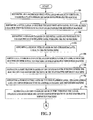
Figures 3-4 are flowcharts of a method for manufacturing the infrared sensor ofFigure 2 in accordance with another exemplary embodiment; -
Figure 5 is a cross-sectional view of an infrared sensor in accordance with another exemplary embodiment; -
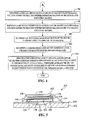
Figures 6-7 are flowcharts of a method for manufacturing the infrared sensor ofFigure 5 in accordance with another exemplary embodiment; -
Figure 8 is a cross-sectional view of an infrared sensor in accordance with another exemplary embodiment; and -
Figure 9 is a flowchart of a method for manufacturing the infrared sensor ofFigure 8 in accordance with another exemplary embodiment. - Referring to
Figure 1 , amanufacturing system 10 for manufacturing the infrared sensors described herein is illustrated. Themanufacturing system 10 includes a plasma enhanced chemicalvapor deposition machine 12, anevaporative deposition machine 14, a sol-gel deposition machine 16, a reactivesputter deposition machine 18, and a metallo-organic decomposition machine 19. - The plasma enhanced chemical
vapor deposition machine 12 is provided to deposit or form a layer of a particular chemical compound on another layer. For example, themachine 12 can deposit an electrically insulative layer such as a low temperature oxide layer on another layer. Further, for example, themachine 12 can deposit a germanium layer, a silicon nitride layer, and an oxynitride layer, on another layer. - The
evaporative deposition machine 14 is provided to deposit or form a layer of a particular chemical compound on another layer. For example, themachine 14 can deposit a titanium layer and a platinum layer on another layer. - The sol-
gel deposition machine 16 is provided to deposit or form a ferroelectric layer on another layer. The ferroelectric layer can comprise one of a strontium bismuth tantalate layer, a barium strontium titanate layer, a lead zirconate titanate layer, or the like, for example. - The reactive
sputter deposition machine 18 is provided to deposit or form a layer of a particular chemical compound on another layer. For example, themachine 18 can deposit on another layer one or more of the following layers: a titanium layer, a platinum layer, and a chrome oxide layer. - The metallo-
organic decomposition machine 19 is provided to deposit or form a ferroelectric layer on another layer. The ferroelectric layer can comprise one of a strontium bismuth tantalate layer, a barium strontium titanate layer, a lead zirconate titanate layer, or the like, for example. - Referring to
Figure 2 , aninfrared sensor 30 for detecting infrared energy in accordance with an exemplary embodiment is illustrated. Theinfrared sensor 30 includes asilicon substrate 32, an on-chip integratedcircuit 34, an electricallyinsulative layer 36, ametal layer 38, agermanium layer 40, asilicon nitride layer 44, atitanium layer 46, aplatinum layer 48, aferroelectric layer 50, aplatinum layer 52,aluminum pads oxynitride layer 58, and achrome oxide layer 60. It should be noted that during manufacture of theinfrared sensor 30, thegermanium layer 40 is removed. - The
silicon substrate 32 is provided to hold the on-chip integratedcircuit 34 and other layers including an infrared sensing structure thereon. The on-chip integratedcircuit 34 can be electrically coupled to thealuminum pads aluminum pads infrared sensor 30 and further indicative of an amount of infrared energy being emitted from the environment that is received by theinfrared sensor 30. - The
electrically insulative layer 36 is provided to electrically insulate the on-chip integratedcircuit 34 from the layers disposed on or above thelayer 36. Thelayer 36 is disposed between thesilicon substrate 32 and themetal layer 42. In one exemplary embodiment, thelayer 36 comprises a low temperature oxide. Of course, in alternative embodiments, thelayer 36 can comprise other types of insulative materials known to those skilled in the art. - The
metal layer 38 is provided to reflect infrared energy received by theinfrared sensor 30 upwardly toward an infrared sensing structure. In one exemplary embodiment, thelayer 38 comprises a titanium layer. In another exemplary embodiment, thelayer 38 comprises a platinum layer. - The
germanium layer 40 is provided to temporarily hold thesilicon nitride layer 44 thereon, and to subsequently allow the formation of acavity 42 in theinfrared sensor 30 when thegermanium layer 40 is removed or dissolved. Thegermanium layer 40 is disposed between themetal layer 38 and thesilicon nitride layer 44. - The
silicon nitride layer 44 is provided hold an infrared sensing structure thereon. Thesilicon nitride layer 44 is a generally U-shaped structure disposed between thegermanium layer 40 and thetitanium layer 46. - The
titanium layer 46 is provided to bond to thesilicon nitride layer 44. Thetitanium layer 46 is disposed between the silicon nitride layer and theplatinum layer 48, and thus thetitanium layer 46 promotes an adhesion of theplatinum layer 48. - A combination of the
platinum layer 48, theferroelectric layer 50, and theplatinum layer 52 comprises an infrared sensing structure that generates an output voltage indicative of a temperature of theinfrared sensor 30. Theplatinum layer 48 is disposed between thetitanium layer 46 and theferroelectric layer 50. Theferroelectric layer 50 is disposed between the platinum layers 48, 52. Theferroelectric layer 50 can comprise one of a strontium bismuth tantalate layer, a barium strontium titanate layer, a lead zirconate titanate layer, or another ferroelectric layer or material known to those skilled in the art. - The
aluminum pads aluminum pads infrared sensor 30 to measure an output voltage of the infrared sensing structure which is indicative of a temperature of theinfrared sensor 30. - The
oxynitride layer 58 is provided to assist in absorbing infrared energy. In one exemplary embodiment, thelayer 58 absorbs infrared energy having a wavelength in a range of 7-12 microns. Theoxynitride layer 58 is disposed between theplatinum layer 52 and thechrome oxide layer 60. - The
chrome oxide 60 is provided to assist in absorbing infrared energy. In one exemplary embodiment, thelayer 60 absorbs infrared energy having a wavelength in a range of 7-12 microns. Thechrome oxide layer 60 is disposed on theoxynitride layer 58. - Referring to
Figures 3-4 , a method for manufacturing theinfrared sensor 30 utilizing themanufacturing system 10 will now be explained. - At
step 80, theelectrically insulative layer 36 is deposited on thesilicon substrate 32, utilizing the plasma enhanced chemicalvapor deposition machine 12. - At
step 82, themetal layer 38 is deposited on theelectrically insulative layer 36, utilizing either the reactive sputter deposition machine 28 or theevaporative deposition machine 14. - At step 84, the
germanium layer 40 is deposited on themetal layer 38 and proximate to electrically insulative layer, utilizing thePECVD machine 12. - At
step 86, thesilicon nitride layer 44 is deposited on thegermanium layer 40, utilizing thePECVD machine 12. - At
step 88, thetitanium layer 46 is deposited on thesilicon nitride layer 44, utilizing either the reactivesputter deposition machine 18 or theevaporative deposition machine 14. - At step 90, the
platinum layer 48 is deposited on thetitanium layer 46, utilizing either the reactivesputter deposition machine 18 or theevaporative deposition machine 14. - At step 92, the
ferroelectric layer 50 is deposited on theplatinum layer 48, utilizing either the sol-gel deposition machine 16 or the metallo-organic decomposition machine 19. - At step 94, the
platinum layer 52 is deposited on theferroelectric layer 50, utilizing either the reactivesputter deposition machine 18 or theevaporative deposition machine 14. - At
step 96, thealuminum pad 54 is deposited on a portion of theplatinum layer 48, utilizing either the reactivesputter deposition machine 18 or theevaporative deposition machine 14. - At
step 98, thealuminum pad 56 is deposited on a portion of theplatinum layer 52, utilizing either the reactivesputter deposition machine 18 or theevaporative deposition machine 14. - At
step 100, theoxynitride layer 58 is deposited on a portion of theplatinum layer 52, utilizing thePECVD machine 12. - At
step 102, thechrome oxide layer 60 is deposited on theoxynitride layer 58, utilizing the reactivesputter deposition machine 18. - At
step 104, thegermanium layer 40 is removed by applying a liquid on thegermanium layer 40 that dissolves thegermanium layer 40 such that thecavity 42 is formed between theelectrically insulative layer 36 and thesilicon nitride layer 44. In one exemplary embodiment, the liquid is hydrogen peroxide. Thecavity 42 is configured to capture a portion of infrared energy therein that is received by the infrared sensing structure. Afterstep 104, the method is exited. - Referring to
Figure 5 , aninfrared sensor 120 for detecting infrared energy in accordance with another exemplary embodiment is illustrated. Theinfrared sensor 120 includes asilicon substrate 122, an on-chipintegrated circuit 123, an electricallyinsulative layer 124, ametal layer 126, agermanium layer 128, atitanium layer 132, aplatinum layer 134, aferroelectric layer 136, aplatinum layer 138,aluminum pads oxynitride layer 144, and achrome oxide layer 146. It should be noted that during manufacture of theinfrared sensor 120, thegermanium layer 128 is removed. - The
silicon substrate 122 is provided to hold the on-chipintegrated circuit 123 and other layers including an infrared sensing structure thereon. The on-chipintegrated circuit 123 can be electrically coupled to thealuminum pads aluminum pads - The
electrically insulative layer 124 is provided to electrically insulate the on-chipintegrated circuit 123 from the layers disposed on or above thelayer 124. Thelayer 124 is disposed between thesilicon substrate 122 and themetal layer 126. In one exemplary embodiment, thelayer 124 comprises a low temperature oxide. Of course, in alternative embodiments, thelayer 124 can comprise other types of insulative materials known to those skilled in the art. - The
metal layer 126 is provided to reflect infrared energy received by theinfrared sensor 120 upwardly toward an infrared sensing structure. In one exemplary embodiment, thelayer 128 comprises a titanium layer. In another exemplary embodiment, thelayer 128 comprises a platinum layer. - The
germanium layer 128 is provided to temporarily hold thetitanium layer 132 thereon, and to subsequently allow the formation of acavity 130 in theinfrared sensor 120 when thegermanium layer 128 is removed or dissolved. Thegermanium layer 128 is disposed between themetal layer 126 and thetitanium layer 132. - The
titanium layer 132 is provided to bond to thegermanium layer 128. Thetitanium layer 132 is disposed between the silicon nitride layer and theplatinum layer 134. - A combination of the
platinum layer 134, theferroelectric layer 136, and theplatinum layer 138 comprises an infrared sensing structure that generates an output voltage indicative of a temperature of theinfrared sensor 120. Theplatinum layer 134 is disposed between thetitanium layer 132 and theferroelectric layer 136. Theferroelectric layer 136 is disposed between the platinum layers 134, 138. Theferroelectric layer 136 can comprise one of a strontium bismuth tantalate layer, a barium strontium titanate layer, a lead zirconate titanate layer, or another ferroelectric layer or material known to those skilled in the art. - The
aluminum pads aluminum pads infrared sensor 120 to measure an output electric charge change of the infrared sensing structure which is indicative of a temperature of theinfrared sensor 30. - The
oxynitride layer 144 is provided to assist in absorbing infrared energy. In one exemplary embodiment, thelayer 144 absorbs infrared energy having a wavelength in a range of 7-12 microns. Theoxynitride layer 144 is disposed between theplatinum layer 138 and thechrome oxide layer 146. - The
chrome oxide layer 146 is provided to assist in absorbing infrared energy. In one exemplary embodiment, thelayer 146 absorbs infrared energy having a wavelength in a range of 7-12 microns. Thechrome oxide layer 146 is disposed on theoxynitride layer 144. - Referring to
Figures 6-7 , a method for manufacturing theinfrared sensor 30 utilizing themanufacturing system 10 will now be explained. - At
step 160, the electricallyinsulative layer 124 is deposited on thesilicon substrate 122, utilizing thePECVD machine 12. - At
step 162, themetal layer 126 is deposited on theelectrically insulative layer 124, utilizing either the reactivesputter deposition machine 18 or theevaporative deposition machine 14. - At
step 164, thegermanium layer 128 is deposited on themetal layer 126 proximate to theelectrically insulative layer 124, utilizing thePECVD machine 12. - At
step 166, thetitanium layer 132 is deposited on thegermanium layer 128, utilizing either the reactivesputter deposition machine 18 or theevaporative deposition machine 14. - At
step 168, theplatinum layer 134 is deposited on thetitanium layer 132, utilizing either the reactivesputter deposition machine 18 or theevaporative deposition machine 14. - At
step 170, theferroelectric layer 136 is deposited on theplatinum layer 134, utilizing either the sol-gel deposition machine 16 or the metallo-organic decomposition machine 19. - At
step 172, theplatinum layer 138 is deposited on theferroelectric layer 136, utilizing either the reactivesputter deposition machine 18 or theevaporative deposition machine 14. - At
step 174, thealuminum pad 140 is deposited on a portion of theplatinum layer 138, utilizing either the reactivesputter deposition machine 18 or theevaporative deposition machine 14. - At
step 176, thealuminum pad 142 is deposited on a portion of theplatinum layer 138, utilizing either the reactivesputter deposition machine 18 or theevaporative deposition machine 14. - At
step 178, theoxynitride layer 144 is deposited on a portion of theplatinum layer 138, utilizing thePECVD machine 12. - At
step 180, thechrome oxide layer 144 is deposited on theoxynitride layer 144, utilizing the reactivesputter deposition machine 18. - At
step 182, thegermanium layer 128 is removed by applying a liquid on thegermanium layer 128 that dissolves thegermanium layer 128 such that thecavity 130 is formed between theelectrically insulative layer 124 and thetitanium layer 132. In one exemplary embodiment, the liquid is hydrogen peroxide. Thecavity 130 is configured to capture a portion of infrared energy therein that is received by the infrared sensing structure. Afterstep 182, the method is exited. - Referring to
Figure 8 , aninfrared sensor 200 for detecting infrared energy in accordance with another exemplary embodiment is illustrated. Theinfrared sensor 200 includes a silicon substrate 202, agermanium layer 204, aplatinum layer 208, aferroelectric layer 210, and aplatinum layer 212. It should be noted that during manufacture of theinfrared sensor 200, thegermanium layer 204 is removed to form acavity 206. - The silicon substrate 202 is provided to hold the other layers including an infrared sensing structure thereon. The silicon substrate 202 may have an integrated circuit 209 thereon which is electrically coupled to the electrically
conductive layers layers layers layers - The
germanium layer 204 is provided to temporarily hold the electricallyconductive layer 208 thereon, and to subsequently allow the formation of thecavity 206 in theinfrared sensor 200 when thegermanium layer 204 is removed or dissolved. Thegermanium layer 204 is disposed between the silicon substrate 202 and the electricallyconductive layer 208. - A combination of the electrically
conductive layer 208, theferroelectric layer 210, and the electricallyconductive layer 212 comprises an infrared sensing structure that generates an output voltage indicative of a temperature of theinfrared sensor 200. The electricallyconductive layer 208 is disposed between thegermanium layer 206 and theferroelectric layer 210. Theferroelectric layer 210 is disposed between the electricallyconductive layers ferroelectric layer 210 can comprise one of a strontium bismuth tantalate layer, a barium strontium titanate layer, a lead zirconate titanate layer, or another ferroelectric layer or material known to those skilled in the art. The electricallyconductive layers - Referring to
Figure 9 , a method for manufacturing theinfrared sensor 200 utilizing themanufacturing system 10 will now be explained. - At
step 230, thegermanium layer 204 is deposited on the silicon substrate 202, utilizing thePECVD machine 12. - At
step 232, the electricallyconductive layer 208 is deposited on thegermanium layer 204 and a portion of the silicon substrate 202, utilizing either the reactivesputter deposition machine 18 or theevaporative deposition machine 14. - At
step 234, the ferro-electric layer 210 is deposited on the electricallyconductive layer 208 opposite thegermanium layer 204, utilizing either the sol-gel deposition device 16 or the metallo-organic decomposition machine 19. - At
step 236, the electricallyconductive layer 212 is deposited on the ferro-electric layer 210 and a portion of the silicon substrate 202, utilizing either the reactivesputter deposition machine 18 or theevaporative deposition machine 14. - At
step 238, thegermanium layer 204 is removed by applying a liquid on thegermanium layer 204 that dissolves thegermanium layer 204 such that thecavity 206 is formed between the electricallyconductive layer 208 and the silicon substrate 202. In one exemplary embodiment, the liquid is hydrogen peroxide. Thecavity 206 is configured to capture a portion of infrared energy therein that is received by the electricallyconductive layer 212, theferroelectric layer 210, and the electricallyconductive layer 208. Afterstep 236, the method is exited. - The infrared sensors and the methods for manufacturing the infrared sensors represent a substantial improvement over other sensors and methods. In particular, the methods for manufacturing the infrared sensors provide a technical effect of depositing an infrared sensing structure on a silicon substrate and forming a cavity between the infrared sensing structure and the silicon substrate for capturing infrared energy.
- While the invention has been described with reference to exemplary embodiments, it will be understood by those skilled in the art that various changes may be made and equivalent elements may be substituted for elements thereof without departing from the scope of the invention. In addition, many modifications may be made to adapt a particular situation or material to the teachings of the invention without departing from the essential scope thereof. Therefore, it is intended that the invention not be limited to the particular embodiments disclosed for carrying out this invention, but that the invention will include all embodiments falling within the scope of the appended claims. Moreover, the use of the terms first, second, etc. do not denote any order or importance, but rather the terms first, second, etc. are used to distinguish one element from another. Further, the use of the terms a, an, etc. do not denote a limitation of quantity, but rather denote the presence of at least one of the referenced item.
Claims (20)
- A method for manufacturing an infrared sensor (30), comprising:depositing an electrically insulative layer (36) on a silicon substrate (32);depositing a germanium layer (40) proximate to the electrically insulative layer (36);depositing a silicon nitride layer (44) on a side of the germanium layer (40) opposite the electrically insulative layer (36);depositing a titanium layer (46) on the silicon nitride layer (44);disposing an infrared sensing structure on the titanium layer (46); andremoving the germanium layer (40) by applying a liquid on the germanium layer (40) that dissolves the germanium layer (40) such that a cavity (42) is formed between the electrically insulative layer (36) and the silicon nitride layer (44), the cavity (42) configured to capture a portion of infrared energy therein that is received by the infrared sensing structure.
- The method of claim 1, wherein the infrared sensing structure comprises a first platinum layer (48), a ferroelectric layer (50), and a second platinum layer (52),
wherein disposing the infrared sensing structure on the titanium layer (46), comprises:depositing the first platinum layer (48) on the titanium layer (46);depositing the ferroelectric layer (50) on the first platinum layer (48); anddepositing the second platinum layer (52) on the ferroelectric layer (50). - The method of claim 1, wherein the ferroelectric layer (50) comprises one of a strontium bismuth tantalate layer, a barium strontium titanate layer, and a lead zirconate titanate layer.
- The method of claim 2, further comprising:depositing a first aluminum pad (56) on a portion of the first platinum layer (48); and depositing a second aluminum pad (54) on a portion of the second platinum layer (52).
- The method of claim 1, further comprising depositing a metal layer (38) on the electrically insulative layer (36) between the electrically insulative layer (36) and at least a portion of the germanium layer (40).
- The method of claim 5, wherein the metal layer (38) comprises another titanium layer or a platinum layer.
- The method of claim 1, further comprising:depositing an oxynitride layer (58) on the infrared sensing structure; anddepositing a chrome oxide layer (60) on the oxynitride layer (58).
- An infrared sensor (30), comprising:a silicon substrate (32);an electrically insulative layer (36) disposed on the silicon substrate (32);a silicon nitride layer (44) disposed proximate to the electrically insulative layer (36) such that a cavity (42) is formed therebetween;a titanium layer (46) disposed on a side of the silicon nitride layer (44) opposite the electrically insulative layer (36); andan infrared sensing structure disposed on the titanium layer (46) configured to generate a signal indicative of an amount of infrared energy being received by the infrared sensing structure, the cavity (42) configured to capture a portion of the infrared energy that is received by the infrared sensing structure.
- The infrared sensor of claim 8, wherein the infrared sensing structure comprises:a first platinum layer (48) disposed on the titanium layer (46);a ferroelectric layer (50) disposed on the first platinum layer (48); anda second platinum layer (52) disposed on the ferroelectric layer (50).
- The infrared sensor of claim 9, wherein the ferroelectric layer (50) comprises one of a strontium bismuth tantalate layer, a barium strontium titanate layer, and a lead zirconate titanate layer.
- The infrared sensor of claim 9, further comprising:a first aluminum pad (56) disposed on a portion of the first platinum layer (48); anda second aluminum pad (54) disposed on a portion of the second platinum layer (52).
- The infrared sensor of claim 8, further comprising a metal layer disposed on the electrically insulative layer between the electrically insulative layer and at least a portion of the germanium layer.
- The infrared sensor of claim 12, wherein the metal layer (38) comprises another titanium layer or a platinum layer.
- The infrared sensor of claim 8, further comprising:an oxynitride layer (58) disposed on the infrared sensing structure; anda chrome oxide layer (60) disposed on the oxynitride layer (58).
- A method for manufacturing an infrared sensor (120), comprising:depositing an electrically insulative layer (124) on a silicon substrate (122);depositing a germanium layer (128) proximate to the electrically insulative layer (124);depositing a titanium (132) layer on the germanium layer (128);disposing an infrared sensing structure on the titanium layer (132); andremoving the germanium layer (128) by applying a liquid on the germanium layer (128) that dissolves the germanium layer (128) such that a cavity (130) is formed between the electrically insulative layer (124) and the titanium layer (132), the cavity (130) configured to capture a portion of infrared energy therein that is received by the infrared sensing structure.
- The method of claim 15, wherein the infrared sensing structure comprises a first platinum layer (134), a ferroelectric layer (136), and a second platinum layer (138),
wherein disposing the infrared sensing structure on the titanium layer (132) comprises:depositing the first platinum layer (134) on the titanium layer (132);depositing the ferroelectric layer (136) on the first platinum layer (134); anddepositing the second platinum layer (138) on the ferroelectric layer (136). - An infrared sensor (120), comprising:a silicon substrate (122);an electrically insulative layer (124) disposed on the silicon substrate (122);a titanium layer (132) disposed proximate to the electrically insulative layer (124) such that a cavity (130) is formed therebetween; andan infrared sensing structure disposed on the titanium layer (132) configured to generate a signal indicative of an amount of infrared energy being received by the infrared sensing structure, the cavity (130) capturing a portion of the infrared energy received by the infrared sensing structure therein.
- The infrared sensor of claim 17, wherein the infrared sensing structure comprises:a first platinum layer (134) disposed on the titanium layer (132);a ferroelectric layer (136) disposed on the first platinum layer (134); anda second platinum layer (138) disposed on the ferroelectric layer (136).
- A method for manufacturing an infrared sensor (200), comprising:depositing a germanium layer (204) on a silicon substrate (202);depositing a first electrically conductive layer (208) on both the germanium layer (204) and a portion of the silicon substrate (202);depositing a ferroelectric layer (210) on the first electrically conductive layer (208) opposite the germanium layer (204);depositing a second electrically conductive layer (212) on both the ferroelectric layer (210) and a portion of the silicon substrate (202); andremoving the germanium layer (204) by applying a liquid on the germanium layer (204) that dissolves the germanium layer (204) such that a cavity (206) is formed between the first electrically conductive layer (208) and the silicon substrate (202), the cavity (206) configured to capture a portion of infrared energy therein that is received by the first electrically conductive layer (208), the ferroelectric layer (210), and the second electrically conductive layer (212).
- An infrared sensor (200), comprising:a silicon substrate (202);a first electrically conductive layer (208) disposed on a portion of the silicon substrate (202) such that a cavity (206) is formed between a portion of the first electrically conductive layer (208) and the silicon substrate (202);a ferroelectric layer (210) disposed on the first electrically conductive layer (208) opposite the cavity (206); anda second electrically conductive layer (212) disposed on both the ferroelectric layer (210) and another portion of the silicon substrate (202); the first electrically conductive layer (208), the ferroelectric layer (210), and the second electrically conductive layer (212) being configured to generate a signal indicative of an amount of infrared energy being received by the first electrically conductive layer (208), the ferroelectric layer (210), and the second electrically conductive layer (212); the cavity (206) being configured to capture a portion of the infrared energy received by the first electrically conductive layer (208), the ferroelectric layer (210) and the second electrically conductive layer (212).
Applications Claiming Priority (1)
| Application Number | Priority Date | Filing Date | Title |
|---|---|---|---|
| US11/671,662 US20080185522A1 (en) | 2007-02-06 | 2007-02-06 | Infrared sensors and methods for manufacturing the infrared sensors |
Publications (2)
| Publication Number | Publication Date |
|---|---|
| EP1956658A2 true EP1956658A2 (en) | 2008-08-13 |
| EP1956658A3 EP1956658A3 (en) | 2011-03-23 |
Family
ID=39432618
Family Applications (1)
| Application Number | Title | Priority Date | Filing Date |
|---|---|---|---|
| EP08151080A Withdrawn EP1956658A3 (en) | 2007-02-06 | 2008-02-05 | Ferroelectric infrared sensors and methods for their manufacturing |
Country Status (2)
| Country | Link |
|---|---|
| US (1) | US20080185522A1 (en) |
| EP (1) | EP1956658A3 (en) |
Cited By (1)
| Publication number | Priority date | Publication date | Assignee | Title |
|---|---|---|---|---|
| WO2010080815A1 (en) * | 2009-01-07 | 2010-07-15 | Robert Bosch Gmbh | Electromagnetic radiation sensor and method of manufacture |
Families Citing this family (1)
| Publication number | Priority date | Publication date | Assignee | Title |
|---|---|---|---|---|
| CN111115558A (en) * | 2019-12-31 | 2020-05-08 | 杭州士兰集成电路有限公司 | Infrared sensor device and method for manufacturing same |
Family Cites Families (23)
| Publication number | Priority date | Publication date | Assignee | Title |
|---|---|---|---|---|
| US5021663B1 (en) * | 1988-08-12 | 1997-07-01 | Texas Instruments Inc | Infrared detector |
| US5286976A (en) * | 1988-11-07 | 1994-02-15 | Honeywell Inc. | Microstructure design for high IR sensitivity |
| US5288649A (en) * | 1991-09-30 | 1994-02-22 | Texas Instruments Incorporated | Method for forming uncooled infrared detector |
| JP3287173B2 (en) * | 1995-04-07 | 2002-05-27 | 三菱電機株式会社 | Infrared detector |
| US5945673A (en) * | 1996-08-30 | 1999-08-31 | Raytheon Company | Thermal detector with nucleation element and method |
| EP0867701A1 (en) * | 1997-03-28 | 1998-09-30 | Interuniversitair Microelektronica Centrum Vzw | Method of fabrication of an infrared radiation detector and more particularly an infrared sensitive bolometer |
| US5927206A (en) * | 1997-12-22 | 1999-07-27 | Eastman Kodak Company | Ferroelectric imaging member and methods of use |
| WO2000042231A2 (en) * | 1999-01-15 | 2000-07-20 | The Regents Of The University Of California | Polycrystalline silicon germanium films for forming micro-electromechanical systems |
| JP3460810B2 (en) * | 1999-07-26 | 2003-10-27 | 日本電気株式会社 | Thermal infrared detector with thermal separation structure |
| DE19961180C2 (en) * | 1999-12-18 | 2002-02-28 | Daimler Chrysler Ag | Thin-film resistor with high temperature coefficient as a passive semiconductor component for integrated circuits and manufacturing processes |
| JP3921320B2 (en) * | 2000-01-31 | 2007-05-30 | 日本電気株式会社 | Thermal infrared detector and method for manufacturing the same |
| US6690014B1 (en) * | 2000-04-25 | 2004-02-10 | Raytheon Company | Microbolometer and method for forming |
| US7879448B2 (en) * | 2000-07-11 | 2011-02-01 | Guardian Industires Corp. | Coated article with low-E coating including IR reflecting layer(s) and corresponding method |
| TW512524B (en) * | 2001-01-19 | 2002-12-01 | Nat Science Council | Fabrication of amorphous silicon/amorphous silicon gemine NI1PI2N infrared position defectors |
| JP3974338B2 (en) * | 2001-03-15 | 2007-09-12 | 株式会社東芝 | Infrared detector and infrared detector |
| US6828172B2 (en) * | 2002-02-04 | 2004-12-07 | Delphi Technologies, Inc. | Process for a monolithically-integrated micromachined sensor and circuit |
| US6939015B2 (en) * | 2002-09-20 | 2005-09-06 | Eastman Kodak Company | Chromium black light shield |
| US7071007B2 (en) * | 2002-12-06 | 2006-07-04 | Taiwan Semiconductor Manufacturing Co., Ltd. | Method of forming a low voltage drive ferroelectric capacitor |
| US7564021B2 (en) * | 2003-02-21 | 2009-07-21 | Delphi Technologies, Inc. | Pyroelectric sensor |
| DE10352001A1 (en) * | 2003-11-07 | 2005-06-09 | Robert Bosch Gmbh | Micromechanical component with a membrane and method for producing such a component |
| KR100658114B1 (en) * | 2004-09-17 | 2006-12-14 | 한국과학기술연구원 | Infrared Absorption Layer Structure and Formation Method and Uncooled Infrared Sensing Device Using the Same |
| US7157300B2 (en) * | 2004-11-19 | 2007-01-02 | Sharp Laboratories Of America, Inc. | Fabrication of thin film germanium infrared sensor by bonding to silicon wafer |
| US7262412B2 (en) * | 2004-12-10 | 2007-08-28 | L-3 Communications Corporation | Optically blocked reference pixels for focal plane arrays |
-
2007
- 2007-02-06 US US11/671,662 patent/US20080185522A1/en not_active Abandoned
-
2008
- 2008-02-05 EP EP08151080A patent/EP1956658A3/en not_active Withdrawn
Cited By (2)
| Publication number | Priority date | Publication date | Assignee | Title |
|---|---|---|---|---|
| WO2010080815A1 (en) * | 2009-01-07 | 2010-07-15 | Robert Bosch Gmbh | Electromagnetic radiation sensor and method of manufacture |
| US7842533B2 (en) | 2009-01-07 | 2010-11-30 | Robert Bosch Gmbh | Electromagnetic radiation sensor and method of manufacture |
Also Published As
| Publication number | Publication date |
|---|---|
| US20080185522A1 (en) | 2008-08-07 |
| EP1956658A3 (en) | 2011-03-23 |
Similar Documents
| Publication | Publication Date | Title |
|---|---|---|
| US10770500B2 (en) | Solid state imaging device for reducing dark current | |
| US11623246B2 (en) | Piezoelectric micromachined ultrasound transducer device with piezoelectric barrier layer | |
| US20070062812A1 (en) | Gas sensor and method for the production thereof | |
| CN202204598U (en) | Sensor component and infrared sensor | |
| EP2720034B1 (en) | Integrated Circuit comprising a relative humidity sensor and a thermal conductivity based gas sensor | |
| US7726198B2 (en) | Strain sensor | |
| CN110346423B (en) | A CMOS-MEMS Humidity Sensor | |
| CN101004398A (en) | Humidity sensor and semiconductor device including the same | |
| US10914638B2 (en) | Pyroelectric sensor | |
| CN102449453B (en) | Infrared light sensor having a high signal voltage and a high signal/noise ratio | |
| EP2924402A1 (en) | Infrared detecting device | |
| WO2021109999A1 (en) | Humidity sensor and manufacturing method therefor | |
| US20130320481A1 (en) | High Density Pyroelectric Thin Film Infrared Sensor Array and Method of Manufacture Thereof | |
| EP1956658A2 (en) | Ferroelectric infrared sensors and methods for their manufacturing | |
| KR101073633B1 (en) | method for manufacturing flexible sensor, flexible sensor manufactured by the same | |
| US20110127674A1 (en) | Layer structure for electrical contacting of semiconductor components | |
| JP5419139B2 (en) | Semiconductor integrated device and manufacturing method thereof | |
| TW202012923A (en) | Piezoelectric biosensor and related forming method | |
| JP2008149451A (en) | Micromachined component with integrated passive electronic component and method for making a micromachined component | |
| CN115959620A (en) | Inertial sensor, preparation method thereof and electronic equipment | |
| US20130305830A1 (en) | Pressure sensor element | |
| CN107923934A (en) | Capacitance structure and the method that the quantity of electric charge is determined in the case of using capacitance structure | |
| EP3214434B1 (en) | Method for fabrication of a sensor device | |
| CN214200388U (en) | Infrared thermopile sensor | |
| WO2025160741A1 (en) | Electrode structure, ultrasonic transducer, ultrasonic transducer manufacturing process, and electronic device |
Legal Events
| Date | Code | Title | Description |
|---|---|---|---|
| PUAI | Public reference made under article 153(3) epc to a published international application that has entered the european phase |
Free format text: ORIGINAL CODE: 0009012 |
|
| AK | Designated contracting states |
Kind code of ref document: A2 Designated state(s): AT BE BG CH CY CZ DE DK EE ES FI FR GB GR HR HU IE IS IT LI LT LU LV MC MT NL NO PL PT RO SE SI SK TR |
|
| AX | Request for extension of the european patent |
Extension state: AL BA MK RS |
|
| PUAL | Search report despatched |
Free format text: ORIGINAL CODE: 0009013 |
|
| AK | Designated contracting states |
Kind code of ref document: A3 Designated state(s): AT BE BG CH CY CZ DE DK EE ES FI FR GB GR HR HU IE IS IT LI LT LU LV MC MT NL NO PL PT RO SE SI SK TR |
|
| AX | Request for extension of the european patent |
Extension state: AL BA MK RS |
|
| AKY | No designation fees paid | ||
| REG | Reference to a national code |
Ref country code: DE Ref legal event code: R108 |
|
| REG | Reference to a national code |
Ref country code: DE Ref legal event code: R108 Effective date: 20111130 |
|
| STAA | Information on the status of an ep patent application or granted ep patent |
Free format text: STATUS: THE APPLICATION IS DEEMED TO BE WITHDRAWN |
|
| 18D | Application deemed to be withdrawn |
Effective date: 20110901 |