EP1956401B1 - Display device with a bottom chassis - Google Patents
Display device with a bottom chassis Download PDFInfo
- Publication number
- EP1956401B1 EP1956401B1 EP08150351A EP08150351A EP1956401B1 EP 1956401 B1 EP1956401 B1 EP 1956401B1 EP 08150351 A EP08150351 A EP 08150351A EP 08150351 A EP08150351 A EP 08150351A EP 1956401 B1 EP1956401 B1 EP 1956401B1
- Authority
- EP
- European Patent Office
- Prior art keywords
- guide plate
- light guide
- display device
- bottom chassis
- peripheral
- Prior art date
- Legal status (The legal status is an assumption and is not a legal conclusion. Google has not performed a legal analysis and makes no representation as to the accuracy of the status listed.)
- Ceased
Links
Images



Classifications
-
- G—PHYSICS
- G02—OPTICS
- G02B—OPTICAL ELEMENTS, SYSTEMS OR APPARATUS
- G02B6/00—Light guides; Structural details of arrangements comprising light guides and other optical elements, e.g. couplings
- G02B6/0001—Light guides; Structural details of arrangements comprising light guides and other optical elements, e.g. couplings specially adapted for lighting devices or systems
- G02B6/0011—Light guides; Structural details of arrangements comprising light guides and other optical elements, e.g. couplings specially adapted for lighting devices or systems the light guides being planar or of plate-like form
- G02B6/0081—Mechanical or electrical aspects of the light guide and light source in the lighting device peculiar to the adaptation to planar light guides, e.g. concerning packaging
- G02B6/0086—Positioning aspects
- G02B6/0088—Positioning aspects of the light guide or other optical sheets in the package
-
- G—PHYSICS
- G02—OPTICS
- G02B—OPTICAL ELEMENTS, SYSTEMS OR APPARATUS
- G02B6/00—Light guides; Structural details of arrangements comprising light guides and other optical elements, e.g. couplings
- G02B6/0001—Light guides; Structural details of arrangements comprising light guides and other optical elements, e.g. couplings specially adapted for lighting devices or systems
- G02B6/0011—Light guides; Structural details of arrangements comprising light guides and other optical elements, e.g. couplings specially adapted for lighting devices or systems the light guides being planar or of plate-like form
- G02B6/0013—Means for improving the coupling-in of light from the light source into the light guide
- G02B6/0015—Means for improving the coupling-in of light from the light source into the light guide provided on the surface of the light guide or in the bulk of it
- G02B6/002—Means for improving the coupling-in of light from the light source into the light guide provided on the surface of the light guide or in the bulk of it by shaping at least a portion of the light guide, e.g. with collimating, focussing or diverging surfaces
- G02B6/0021—Means for improving the coupling-in of light from the light source into the light guide provided on the surface of the light guide or in the bulk of it by shaping at least a portion of the light guide, e.g. with collimating, focussing or diverging surfaces for housing at least a part of the light source, e.g. by forming holes or recesses
-
- G—PHYSICS
- G02—OPTICS
- G02B—OPTICAL ELEMENTS, SYSTEMS OR APPARATUS
- G02B6/00—Light guides; Structural details of arrangements comprising light guides and other optical elements, e.g. couplings
- G02B6/0001—Light guides; Structural details of arrangements comprising light guides and other optical elements, e.g. couplings specially adapted for lighting devices or systems
- G02B6/0011—Light guides; Structural details of arrangements comprising light guides and other optical elements, e.g. couplings specially adapted for lighting devices or systems the light guides being planar or of plate-like form
- G02B6/0033—Means for improving the coupling-out of light from the light guide
- G02B6/0035—Means for improving the coupling-out of light from the light guide provided on the surface of the light guide or in the bulk of it
- G02B6/0045—Means for improving the coupling-out of light from the light guide provided on the surface of the light guide or in the bulk of it by shaping at least a portion of the light guide
- G02B6/0046—Tapered light guide, e.g. wedge-shaped light guide
- G02B6/0048—Tapered light guide, e.g. wedge-shaped light guide with stepwise taper
-
- G—PHYSICS
- G02—OPTICS
- G02F—OPTICAL DEVICES OR ARRANGEMENTS FOR THE CONTROL OF LIGHT BY MODIFICATION OF THE OPTICAL PROPERTIES OF THE MEDIA OF THE ELEMENTS INVOLVED THEREIN; NON-LINEAR OPTICS; FREQUENCY-CHANGING OF LIGHT; OPTICAL LOGIC ELEMENTS; OPTICAL ANALOGUE/DIGITAL CONVERTERS
- G02F1/00—Devices or arrangements for the control of the intensity, colour, phase, polarisation or direction of light arriving from an independent light source, e.g. switching, gating or modulating; Non-linear optics
- G02F1/01—Devices or arrangements for the control of the intensity, colour, phase, polarisation or direction of light arriving from an independent light source, e.g. switching, gating or modulating; Non-linear optics for the control of the intensity, phase, polarisation or colour
- G02F1/13—Devices or arrangements for the control of the intensity, colour, phase, polarisation or direction of light arriving from an independent light source, e.g. switching, gating or modulating; Non-linear optics for the control of the intensity, phase, polarisation or colour based on liquid crystals, e.g. single liquid crystal display cells
- G02F1/133—Constructional arrangements; Operation of liquid crystal cells; Circuit arrangements
- G02F1/1333—Constructional arrangements; Manufacturing methods
- G02F1/133308—Support structures for LCD panels, e.g. frames or bezels
-
- G—PHYSICS
- G02—OPTICS
- G02F—OPTICAL DEVICES OR ARRANGEMENTS FOR THE CONTROL OF LIGHT BY MODIFICATION OF THE OPTICAL PROPERTIES OF THE MEDIA OF THE ELEMENTS INVOLVED THEREIN; NON-LINEAR OPTICS; FREQUENCY-CHANGING OF LIGHT; OPTICAL LOGIC ELEMENTS; OPTICAL ANALOGUE/DIGITAL CONVERTERS
- G02F1/00—Devices or arrangements for the control of the intensity, colour, phase, polarisation or direction of light arriving from an independent light source, e.g. switching, gating or modulating; Non-linear optics
- G02F1/01—Devices or arrangements for the control of the intensity, colour, phase, polarisation or direction of light arriving from an independent light source, e.g. switching, gating or modulating; Non-linear optics for the control of the intensity, phase, polarisation or colour
- G02F1/13—Devices or arrangements for the control of the intensity, colour, phase, polarisation or direction of light arriving from an independent light source, e.g. switching, gating or modulating; Non-linear optics for the control of the intensity, phase, polarisation or colour based on liquid crystals, e.g. single liquid crystal display cells
- G02F1/133—Constructional arrangements; Operation of liquid crystal cells; Circuit arrangements
- G02F1/1333—Constructional arrangements; Manufacturing methods
- G02F1/133308—Support structures for LCD panels, e.g. frames or bezels
- G02F1/133314—Back frames
-
- G—PHYSICS
- G02—OPTICS
- G02F—OPTICAL DEVICES OR ARRANGEMENTS FOR THE CONTROL OF LIGHT BY MODIFICATION OF THE OPTICAL PROPERTIES OF THE MEDIA OF THE ELEMENTS INVOLVED THEREIN; NON-LINEAR OPTICS; FREQUENCY-CHANGING OF LIGHT; OPTICAL LOGIC ELEMENTS; OPTICAL ANALOGUE/DIGITAL CONVERTERS
- G02F1/00—Devices or arrangements for the control of the intensity, colour, phase, polarisation or direction of light arriving from an independent light source, e.g. switching, gating or modulating; Non-linear optics
- G02F1/01—Devices or arrangements for the control of the intensity, colour, phase, polarisation or direction of light arriving from an independent light source, e.g. switching, gating or modulating; Non-linear optics for the control of the intensity, phase, polarisation or colour
- G02F1/13—Devices or arrangements for the control of the intensity, colour, phase, polarisation or direction of light arriving from an independent light source, e.g. switching, gating or modulating; Non-linear optics for the control of the intensity, phase, polarisation or colour based on liquid crystals, e.g. single liquid crystal display cells
- G02F1/133—Constructional arrangements; Operation of liquid crystal cells; Circuit arrangements
- G02F1/1333—Constructional arrangements; Manufacturing methods
- G02F1/1335—Structural association of cells with optical devices, e.g. polarisers or reflectors
- G02F1/1336—Illuminating devices
- G02F1/133615—Edge-illuminating devices, i.e. illuminating from the side
-
- G—PHYSICS
- G02—OPTICS
- G02F—OPTICAL DEVICES OR ARRANGEMENTS FOR THE CONTROL OF LIGHT BY MODIFICATION OF THE OPTICAL PROPERTIES OF THE MEDIA OF THE ELEMENTS INVOLVED THEREIN; NON-LINEAR OPTICS; FREQUENCY-CHANGING OF LIGHT; OPTICAL LOGIC ELEMENTS; OPTICAL ANALOGUE/DIGITAL CONVERTERS
- G02F2201/00—Constructional arrangements not provided for in groups G02F1/00 - G02F7/00
- G02F2201/54—Arrangements for reducing warping-twist
Definitions
- a display device according to the preamble of appended claim 1 is disclosed in JP 2006 235 438 .
- FIG. 1 illustrates a view of a LCD device 100 according to a first comparative example not according to but useful to understand the invention.
- the bottom chassis 122 is indented so that an inner part of the bottom chassis has an indentation sufficient for insertion of one or more of the light guide plate 118, the optical sheets 110, and the LED substrate 114.
- FIG. 10 illustrates a view of the light guide plate 218 shown in FIG. 7 .
Landscapes
- Physics & Mathematics (AREA)
- General Physics & Mathematics (AREA)
- Optics & Photonics (AREA)
- Nonlinear Science (AREA)
- Mathematical Physics (AREA)
- Chemical & Material Sciences (AREA)
- Crystallography & Structural Chemistry (AREA)
- Liquid Crystal (AREA)
- Planar Illumination Modules (AREA)
- Devices For Indicating Variable Information By Combining Individual Elements (AREA)
Description
- The invention relates to a display device having a backlight assembly. More particularly, embodiments pertain to display devices which manufacturing costs are reduced.
- Various flat panel display devices may be capable of reducing weight and volume, which are the disadvantages associated with cathode ray tubes. The flat panel display devices may be classified into, e.g., liquid crystal displays (LCDs), field emission displays (FEDs), plasma display panels (PDPs), organic light emitting diode (OLED) displays, etc.
- Among the various displays, LCDs may be advantageous in terms of miniaturization, light weight, low power consumption, etc. LCDs have gradually been regarded as an alternative route to overcome the disadvantages of the cathode ray tubes. Today, LCDs have been provided in, e.g., cellular phones, personal digital assistants (PDAs), monitors, TVs, etc.
- In the LCDs, a backlight assembly may be provided with numerous components. Accordingly, there has been a problem that the manufacturing cost of the LCD device is increased due to the numerous components.
- A display device according to the preamble of appended
claim 1 is disclosed inJP 2006 235 438 - Embodiments are therefore directed to a display device which substantially overcomes one or more problems due to the limitations and disadvantages of the related art.
- It is therefore a feature of an embodiment to provide a display device capable of having a reduced manufacturing cost.
- It is therefore another feature of an embodiment to provide a display device having fewer parts.
- According to the invention, there is provided a display device that includes the features of appended
claim 1. - Accordingly, a projecting part of the bottom chassis of the display device extends from a peripheral side of the peripheral part at a substantially right angle to the surface of the peripheral part, and the projecting part bends back toward the peripheral side of the peripheral part. LEDs may be on a LED substrate. The LED substrate may be in the inner side part. The display panel may be fixed to the side surface part by an adhesive material. The adhesive material may be adhesive tape. The display device may further include a reflector between the inner side part and the light guide plate. The display device may further include a top chassis on the display panel, the top chassis being fixed to the bottom chassis. The light guide plate may include first holes adapted to accommodate LEDs, and second holes adapted to accommodate components of a flexible printed circuit. The bottom chassis may include an opening part over the first holes and the second holes.
- An outer side of the light guide plate may have at least one step part proceeding from the outer side to an inner side of the light guide plate. The step parts may be opposite to each other on both sides of the light guide plate. The step parts may be on all side surfaces of the light guide plate in a quadrangular form. The display device may further include a reflector between the inner side part and the light guide plate.
- The above and other features and advantages of the present invention will become more apparent to those of ordinary skill in the art by describing in detail exemplary embodiments thereof with reference to the attached drawings, in which:
-
FIG. 1 illustrates an exploded perspective view of a LCD device according to a first comparative example not according to but useful to understand the invention; -
FIG. 2 illustrates an exploded perspective view where a reflector and a top chassis are added to the LCD device ofFIG. 1 ; -
FIG. 3 illustrates a cross-sectional view of the LCD device taken along line IV-IV' ofFIG. 1 when the LCD device is assembled; -
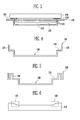
FIG. 4 illustrates a view of a projecting part extended from a bottom chassis shown inFIG. 1 ; -
FIG. 5 illustrates a view where the projecting part ofFIG. 4 bends back toward the peripheral side of the peripheral part of the bottom chassis according to an embodiment of the invention; -
FIG. 6 illustrates a cross-sectional view of the light guide plate ofFIG. 1 ; -
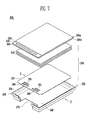
FIG. 7 illustrates an exploded perspective view of a LCD device according to a second comparative example not according to but useful to understand the invention; -
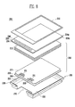
FIG. 8 illustrates an exploded perspective view where a reflector and a top chassis are added to the LCD device ofFIG. 7 ; -
FIG. 9 illustrates a cross-sectional view of the LCD device taken along line X-X' ofFIG. 7 when the LCD device is assembled; and -
FIG. 10 illustrates a cross-sectional view of the light guide plate ofFIG. 7 . - Embodiments and comparative examples will now be described more fully hereinafter with reference to the accompanying drawings, in which comparative examples not according to the invention and an exemplary embodiment of the invention are illustrated.
- In the drawing figures, the dimensions of layers and regions may be exaggerated for clarity of illustration. It will also be understood that when a layer or element is referred to as being "on" another layer or substrate, it can be directly on the other layer or substrate, or intervening layers may also be present. Further, it will be understood that when a layer is referred to as being "under" another layer, it can be directly under, and one or more intervening layers may also be present. In addition, it will also be understood that when a layer is referred to as being "between" two layers, it can be the only layer between the two layers, or one or more intervening layers may also be present. Like reference numerals refer to like elements throughout.
- A display device according to embodiments has a light guide plate and optical sheets inserted into a bottom chassis so that for example a mold frame may be avoided, making it possible to reduce the manufacturing cost. The bottom chassis may be aluminum, and the light guide plate and the optical sheets are inserted in the bottom chassis, which thus imparts higher strength. The light guide plate may be formed with a step part, which may make it possible to prevent the movement of the optical sheets. Although the exemplary embodiment and comparative examples are drawn to a LCD device, the embodiment may be employed for any passive display device requiring light from an external source.
-
FIG. 1 illustrates a view of aLCD device 100 according to a first comparative example not according to but useful to understand the invention. - Referring to
FIG. 1 , theLCD device 100 includes aLCD panel 104, abacklight assembly 150, and a bottom chassis (or a bezel) 122. - The
LCD panel 104 displays a predetermined image. TheLCD panel 104 includes afirst substrate 104a, asecond substrate 104b, and a liquid crystal (not shown) injected between thefirst substrate 104a and thesecond substrate 104b. - The
second substrate 104b may include multiple TFTs arranged in an array. A source electrode of each TFT may be connected to a data line, and a gate electrode thereof may be connected to a scan line. A drain electrode of the TFT may be connected to a pixel electrode of transparent conductive materials, e.g., ITO, indium zinc oxide (IZO), etc. The TFT may be turned-on when a scan signal is supplied to the scan line so that a data signal supplied from the data line may be supplied to the pixel electrode. - An
integrated circuit 106 supplies the data signal and the scan signal. The integratedcircuit 106 may be inserted into one side surface of thesecond substrate 104b. The surroundings of theintegrated circuit 106 may be coated with aprotective layer 108. - The
first substrate 104a is opposite to thesecond substrate 104b. A common electrode of transparent materials, e.g., ITO, IZO, etc., is on a front surface of thefirst substrate 104a. The common electrode is supplied with a predetermined voltage so that a predetermined electric field is formed between the common electrode and the pixel electrode. An array angle of liquid crystal injected between thefirst substrate 104a and thesecond substrate 104b is changed by the electric field, and an optical transmittance is changed according to the changed array angle, thus displaying a desired image. - The
backlight assembly 150 includesLEDs 112, aLED substrate 114, alight guide plate 118, andoptical sheets 110. - The
LEDs 112 generate light having predetermined brightness via a driving signal supplied from theLED substrate 114. - The
LED substrate 114 supplies driving signals to theLEDs 112 corresponding to an externally-supplied control signal. - The
light guide plate 118 supplies light generated by theLEDs 112 to theLCD panel 104. Thelight guide plate 118 supplies light supplied from its side surface to theLCD panel 104 positioned at its upper part. - The
optical sheets 110 improve the brightness of the light, which is supplied from thelight guide plate 118, and supplies the light to theLCD panel 104. - The
bottom chassis 122 includes aside surface part 124 flatly positioned at an outer side surface to surround four edges of an outer part of thebottom chassis 122. Thebottom chassis 122 also includes aninner side part 126 formed to have a predetermined step from theside surface part 124, which allows the insertion of thelight guide plate 118 and theoptical sheets 110. - The
bottom chassis 122 is indented so that an inner part of the bottom chassis has an indentation sufficient for insertion of one or more of thelight guide plate 118, theoptical sheets 110, and theLED substrate 114. - The
inner side part 126 has a predetermined step from theside surface part 124. Theinner side part 126 may therefore have a predetermined height to define a space, into which may be inserted thelight guide plate 118, theoptical sheets 110, theLED substrate 114, and theLEDs 112. - The
side surface part 124 has a predetermined width so that theLCD panel 104 is safely seated. Theside surface part 124 is formed to have a width wider than that of a post, i.e., a step, extending from theinner side part 126 to theside surface part 124. - The
light guide plate 118 and theoptical sheets 110 is inserted into theinner side part 126 of the bottom chassis without employing a mold frame. Omitting the mold frame from the final display construction makes it possible to reduce the manufacturing cost. Thebottom chassis 122 may be, e.g., aluminum, etc., which imparts strength higher than that of a conventional mold frame. The mold frame 16 can therefore be omitted, which may also make it possible to produce a very slim LCD device. - The light incident from the
light guide plate 118 to theinner side part 126 is reflected from theinner side part 126, and is then supplied back to thelight guide plate 118. Since the bottom chassis may be, e.g., aluminum, which may be capable of reflecting light, a reflector (120 ofFIG. 2 ) may be omitted. The strength of thebottom chassis 122 may be high (that is, high strength may be imparted by theside surface part 124 positioned at the four surfaces), which may make it possible to omit a top chassis (102 ofFIG. 2 ). - Referring to
FIG. 2 , thereflector 120 and thetop chassis 102 are added or removed according to the requirements of the display. Thereflector 120 is between thelight guide plate 118 and thebottom chassis 122, and thetop chassis 102 is on theLCD panel 104. Thereflector 120 improves light efficiency by reflecting the light supplied from thelight guide plate 118 back to thelight guide plate 118. Thetop chassis 102 is fixed to thebottom chassis 122 to prevent movement of theLCD panel 104, as well as to impart strength. -
FIG. 3 illustrates a cross-sectional view of the LCD device taken along line IV-IV' ofFIG. 1 when the LCD device is assembled. - Referring to
FIG. 3 , thelight guide plate 118 and theoptical sheets 110 is inserted into theinner side part 126 of thebottom chassis 122. A top surface of theoptical sheets 110 is substantially flush with a top surface of theside surface part 124. After theinner side part 126 is fitted with thelight guide plate 118 and theoptical sheets 110, anadhesive tape 130 is attached to theside surface part 124. Theadhesive tape 130 may be a double sided adhesive tape. TheLCD panel 104 is seated on theadhesive tape 130 so that theLCD panel 104 and thebottom chassis 122 are stably fixed. Theadhesive tape 130 may be replaced with an adhesive material, e.g., silicone, acrylate, epoxy, etc. - Various components may be added in order to improve the strength of the
bottom chassis 122. Referring toFIG. 4 , a projectingpart 128 extends from an outer side of theside surface part 124 of thebottom chassis 122. When thebottom chassis 122 includes the projectingpart 128, the strength of thebottom chassis 122 is increased. When thebottom chassis 122 is formed with the projectingpart 128, externally applied impacts are mitigated by the projectingpart 128 so that theLCD panel 104 therein is stably be protected. The projectingpart 128 may be formed in various forms, e.g., at a substantially right angle from theside surface part 124. As shown inFIG. 5 , in the LCD device according to an embodiment of the invention the projectingpart 128 extends at a substantially right angle from theside surface part 124, and is formed to be bent back toward the outer side of theside surface part 124 at least once, which may make it possible to impart higher strength to thebottom chassis 122. The bends illustrated inFIG. 5 are substantially right angles, but other angles may be used. -
FIG. 6 illustrates a view showing thelight guide 118 plate ofFIG. 1 . - Referring to
FIG. 6 , thelight guide plate 118 hasstep parts 119 in multiple step form. Thestep parts 119 have at least one step, which is lowered a step proceeding from the outer side to the inner side of thelight guide plate 118. Thestep parts 119 prevent movement of theoptical sheets 110 positioned on thelight guide plate 118. When theoptical sheets 110 are seated on thestep parts 119, movement of the optical sheets is prevented by thestep parts 119 so that any degradation due to the movement of theoptical sheets 110 is prevented. - The
step parts 119 may be opposite to each other on both side surfaces of thelight guide plate 118. When thestep parts 119 are opposite to each other on both sides of the outer side region of thelight guide plate 118, movement of theoptical sheets 110 is prevented. Thestep parts 119 may be on all side surfaces of thelight guide plate 118 in a quadrangular form, which further prevents the movement of theoptical sheets 110. -
FIG. 7 illustrates a view of aLCD device 200 according to a second comparative example not according to but useful to understand the invention. - Referring to
FIG. 7 , theLCD device 200 includes aLCD panel 204, abacklight assembly 250, and abottom chassis 222. - The
LCD panel 204 displays a predetermined image. TheLCD panel 204 includes afirst substrate 204a, asecond substrate 204b, and a liquid crystal injected therebetween. - The
second substrate 204b may include multiple TFTs (not shown) arranged in an array. The source electrode of each TFT may be connected to a data line, and the gate electrode of the TFT may be connected to a scan line. The drain electrode of the TFT may be connected to a pixel electrode composed of transparent conductive materials. The TFT may be turned-on when a scan signal is supplied to the scan line so that a data signal supplied from the data line may be supplied to the pixel electrode. - An
integrated circuit 206 is inserted into a side surface of thesecond substrate 204b. Theintegrated circuit 206 supplies the data signal and the scan signal. Aprotective layer 208 is applied to the surroundings of theintegrated circuit 206. Theprotective layer 208 may also cover theintegrated circuit 206. - The
first substrate 204a is arranged opposite to thesecond substrate 204b. A common electrode composed of transparent materials, e.g., ITO, IZO, etc., may be on a front surface of thefirst substrate 204a. The common electrode is supplied with a predetermined voltage so that a predetermined electric field is formed between the common electrode and the pixel electrode. An array angle of liquid crystal injected between thefirst substrate 204a and thesecond substrate 204b is changed by the electric field, and an optical transmittance is changed according to the changed array angle, which thus displays a desired image. - The
backlight assembly 250 includes alight guide plate 218 andoptical sheets 210. - The
light guide plate 218 supplies the light emitted by the LEDs to theLCD panel 204. The light guide plate includesfirst holes 251 andsecond holes 260, where the first andsecond holes light guide plate 218. LEDs may be inserted in thefirst holes 251. The LEDs in thefirst holes 251 may supply a predetermined amount of light to thelight guide plate 218. A flexible printed circuit (FPC) (not shown) may be connected to the LEDs to supply driving signals to the LEDs. The FPC may be connected to the LEDs via thesecond holes 260. Components of the FPC may be inserted in thesecond holes 260. - The
optical sheets 210 improve the brightness of the light, which is supplied from thelight guide plate 218, and supply it to theLCD panel 204. - The
bottom chassis 222 is formed to accommodate the insertion of thelight guide plate 218 and theoptical sheets 210. Thebottom chassis 222 includes a flatly positionedside surface part 224 around a perimeter of the bottom chassis, aninner side part 226 having a predetermined step from theside surface part 124, and a projectingpart 228 extended from an outer side of theside surface part 224. - The
inner side part 226 is formed to have a predetermined step from theside surface part 224. Theinner side part 226 has a predetermined space, wherein the space may accommodate insertion of, e.g., thelight guide plate 218 and theoptical sheets 210. - The
side surface part 224 is positioned to surround all or part of four edges of theinner side part 226, which imparts strength to thebottom chassis 222. The projectingpart 228 extends from theside surface part 224 to impart strength to thebottom chassis 222. - An
opening part 270 is formed in thebottom chassis 222 so as to overlap portions or all of thefirst holes 251 and thesecond holes 260. When theopening part 270 is positioned over portions of thefirst holes 251 and thesecond holes 260, the LEDs, the flexible printed circuit, etc., is easily inserted. - The
light guide plate 218 and theoptical sheets 210 are inserted in theinner side part 226 of thebottom chassis 222 so that a mold frame can be omitted, which makes it possible to reduce the manufacturing cost. Thebottom chassis 222 may be aluminum, etc., which may make it possible to impart higher strength. - The
bottom chassis 222 may be composed of, e.g., reflective aluminum, so that a reflector 220 (seeFIG. 8 ) between thelight guide plate 218 and theinner side part 226 may be removed. The light supplied from thelight guide plate 218 may be reflected from theinner side part 226 so that thereflector 220 may be omitted. Since higher strength may be imparted to thebottom chassis 222, a top chassis 202 (seeFIG. 8 ) may be omitted. - Referring to
FIG. 8 , thereflector 220 and thetop chassis 202 is added. Thereflector 220 between thelight guide plate 218 and thebottom chassis 222 is added, and thetop chassis 202 is arranged on theLCD panel 104. Thereflector 220 improves light efficiency by reflecting light back to thelight guide plate 218. Thetop chassis 202 is fixed to thebottom chassis 222 to prevent the movement of theLCD panel 204 as well as to impart predetermined strength. -
FIG. 9 illustrates a cross-sectional view showing the LCD device taken along line X-X' ofFIG. 8 when the LCD device ofFIG. 8 is assembled. - Referring to
FIG. 9 , thelight guide plate 218 and theoptical sheets 210 are inserted into theinner side part 226 of thebottom chassis 222. After thelight guide plate 218 and theoptical sheets 210 are inserted into theinner side part 226, anadhesive tape 230 is attached to theside surface part 224. Theadhesive tape 230 may be a double sided adhesive tape. TheLCD panel 204 is seated on theadhesive tape 230 so that theLCD panel 204 and thebottom chassis 222 are stably fixed. Theadhesive tape 230 may be replaced with an adhesive material, e.g., silicone, acrylate, epoxy, etc. - The projecting
part 228 extends at a substantially right angle from theside surface part 224, and is formed to be bent toward the outer side of theside surface part 224 at least once (similar to the configuration illustrated inFIG. 5 ), which makes it possible to impart higher strength to thebottom chassis 222. The projectingpart 228 may be omitted from thebottom chassis 222. -
FIG. 10 illustrates a view of thelight guide plate 218 shown inFIG. 7 . - Referring to
FIG. 10 , thelight guide plate 218 is formed withstep parts 219. Thestep parts 219 each have at least one step, which is lowered in step form proceeding from the outer side to the inner side of thelight guide plate 218. Two, three, four or more steps may also be used. Thestep parts 219 prevent the movement of theoptical sheets 210 on thelight guide plate 218. When theoptical sheets 210 are seated in thestep parts 219, movement of theoptical sheets 210 is prevented by thestep parts 219 so that any degradation due to movement of theoptical sheets 210 is prevented. - The
step parts 219 may be opposite to each other on both side surfaces of thelight guide plate 218. When thestep parts 219 are formed to be opposite to each other on both sides of the outer side region of thelight guide plate 218, the movement of theoptical sheets 210 may be prevented to result in a stable construction. Thestep parts 219 may be on all side surfaces of thelight guide plate 218 in a quadrangular form, which may further prevent the movement of theoptical sheets 210. Thelight guide plate 218 may be configured to accommodate thefirst holes 251 and thesecond holes 260.
Claims (11)
- A display device (100), comprising:a display panel (104) ;at least one optical sheet (110) arranged on one side of the display panel (104);a light guide plate (118) arranged on one side of the at least one optical sheet (110) , anda bottom chassis (122) including a peripheral part (124) on the surface of which the display panel (104) is seated, and an inner part (126) relative to said peripheral part (124) which forms a recess by a step formed from the surface of the peripheral part (124), said recess receiving and accommodating the light guide plate (118) and the at least one optical sheet (110) the bottom chassis (122) further including a projecting part (128) extended from a peripheral side of the peripheral part (124), wherein the projecting part (128) first extends at a substantially right angle to said surface of the peripheral part (124)characterised in that, after a predetermined length of said first extension at said substantially right angle, the projecting part (128) bends back toward the peripheral side of the peripheral part (124).
- The display device of claim 1, further including light emitting diodes (112) on a light emitting diode substrate (114), and the light emitting diode substrate (114) is arranged on the peripheral part (124).
- The display device of any of claims 1 to 2, wherein the display panel (104) is fixed to the peripheral part (124) by an adhesive material.
- The display device as claimed in claim 3, wherein the adhesive material is an adhesive tape (130).
- The display device of any of claims 1 to 4, further including a reflector (120) between the inner part (126) and the light guide plate (118, 218).
- The display device of any of claims 1 to 5, further including a top chassis (102) on the display panel (104) the top chassis (102) being fixed to the bottom chassis (122).
- The display device of any of claims 1 and 4 to 6, wherein the light guide plate (118) includes:first holes adapted to accommodate light emitting diodes; andsecond holes adapted to accommodate components of a flexible printed circuit.
- The display device as claimed in claim 7, wherein the bottom chassis (122) includes an opening part over the first holes and the second holes .
- The display device of any of claims 1 to 8, wherein
a recess is formed in one of the major surfaces of the light guide plate (118) by descending step parts (119) , said recess having a shape corresponding to the shape of the at least one optical sheet (110) so that said recess can receive and accommodate said at least one optical sheet (110) - The display device as claimed in claim 9, wherein the one major surface of the light guide plate (118) includes the descending step parts (119) at opposite peripheral sides of said major surface.
- The display device as claimed in claim 9, wherein the one major surface of the light guide plate (118) includes the descending step parts (119) at all peripheral sides of said major surface.
Applications Claiming Priority (2)
| Application Number | Priority Date | Filing Date | Title |
|---|---|---|---|
| KR1020070005321A KR100879852B1 (en) | 2007-01-17 | 2007-01-17 | Liquid crystal display |
| KR1020070012868A KR100873701B1 (en) | 2007-02-07 | 2007-02-07 | Liquid crystal display |
Publications (3)
| Publication Number | Publication Date |
|---|---|
| EP1956401A2 EP1956401A2 (en) | 2008-08-13 |
| EP1956401A3 EP1956401A3 (en) | 2008-08-20 |
| EP1956401B1 true EP1956401B1 (en) | 2009-10-28 |
Family
ID=39509642
Family Applications (1)
| Application Number | Title | Priority Date | Filing Date |
|---|---|---|---|
| EP08150351A Ceased EP1956401B1 (en) | 2007-01-17 | 2008-01-17 | Display device with a bottom chassis |
Country Status (5)
| Country | Link |
|---|---|
| US (1) | US8120722B2 (en) |
| EP (1) | EP1956401B1 (en) |
| JP (1) | JP5038000B2 (en) |
| CN (1) | CN103217824B (en) |
| DE (1) | DE602008000234D1 (en) |
Families Citing this family (31)
| Publication number | Priority date | Publication date | Assignee | Title |
|---|---|---|---|---|
| US20110037740A1 (en) * | 2008-12-15 | 2011-02-17 | Panasonic Corporation | Planar illumination device and liquid crystal display |
| JP4342602B1 (en) * | 2008-12-18 | 2009-10-14 | 株式会社東芝 | Decorative member and video display device |
| KR101533662B1 (en) * | 2009-01-09 | 2015-07-06 | 삼성디스플레이 주식회사 | Display device |
| TWI403786B (en) * | 2009-09-25 | 2013-08-01 | Innolux Corp | Liquid crystal display and assembly method of the same |
| KR101117640B1 (en) * | 2009-10-06 | 2012-03-05 | 삼성모바일디스플레이주식회사 | Flat Panel Display |
| TWI389067B (en) * | 2010-06-29 | 2013-03-11 | Compal Electronics Inc | Display module and assembly method thereof |
| CN202032460U (en) * | 2011-01-25 | 2011-11-09 | 京东方科技集团股份有限公司 | Backlight source lamp shade, backlight source back plate and liquid crystal module |
| TWM411637U (en) * | 2011-04-21 | 2011-09-11 | Even Systems Company Ltd | Touch screen display with built-in privacy filter |
| TWI421575B (en) | 2011-07-04 | 2014-01-01 | Au Optronics Corp | Display apparatus |
| TWI432839B (en) | 2011-08-10 | 2014-04-01 | Au Optronics Corp | Display device |
| US8587745B2 (en) * | 2011-10-24 | 2013-11-19 | Shenzhen China Star Optoelectronics Technology Co., Ltd | Liquid crystal display device and fixing device thereof |
| JP5148775B1 (en) * | 2012-01-13 | 2013-02-20 | シャープ株式会社 | Display device and television receiver |
| CN102759079A (en) * | 2012-07-17 | 2012-10-31 | 深圳市华星光电技术有限公司 | Back plate resisting external force as well as backlight module and liquid crystal display thereof |
| US9084338B2 (en) * | 2012-08-27 | 2015-07-14 | Shenzhen China Star Optoelectronics Technology Co., Ltd. | Display device |
| US9072167B2 (en) * | 2012-08-27 | 2015-06-30 | Shenzhen China Star Optoelectronics Technology Co., Ltd. | Display device |
| US8988875B2 (en) * | 2012-08-27 | 2015-03-24 | Shenzhen China Star Optoelectronics Technology Co., Ltd. | Display device |
| US8988866B2 (en) * | 2012-08-27 | 2015-03-24 | Shenzhen China Star Optoelectronics Technology Co., Ltd. | Display device |
| KR102050382B1 (en) * | 2012-11-28 | 2019-11-29 | 엘지디스플레이 주식회사 | Liquid Display Apparatus |
| WO2014171189A1 (en) * | 2013-04-18 | 2014-10-23 | シャープ株式会社 | Display device |
| KR102035715B1 (en) | 2013-06-27 | 2019-10-24 | 삼성디스플레이 주식회사 | Liquid crystal display |
| JP6188816B2 (en) * | 2013-11-08 | 2017-08-30 | 堺ディスプレイプロダクト株式会社 | Display device |
| KR102169102B1 (en) * | 2013-12-04 | 2020-10-23 | 삼성디스플레이 주식회사 | Bottom chassis for display device and display device comprising the same |
| CN105992623A (en) | 2014-09-26 | 2016-10-05 | 堺显示器制品株式会社 | Display device and method for manufacturing display device |
| CN104503136B (en) * | 2014-12-24 | 2017-07-28 | 青岛海信电器股份有限公司 | A kind of display module and mobile terminal |
| KR20160105605A (en) * | 2015-02-27 | 2016-09-07 | 삼성디스플레이 주식회사 | Display device and fabrication method of the same |
| KR102494154B1 (en) * | 2015-12-31 | 2023-01-31 | 엘지디스플레이 주식회사 | Liquid Crystal Display Device |
| KR102490010B1 (en) * | 2016-05-02 | 2023-01-19 | 삼성디스플레이 주식회사 | Display apparatus |
| TWI613488B (en) * | 2017-06-19 | 2018-02-01 | Au Optronics Corporation | Display panel and method of forming micro component holder |
| CN109597236A (en) | 2018-12-20 | 2019-04-09 | 华为技术有限公司 | The production method of liquid crystal display, electronic equipment and liquid crystal display |
| US11016321B2 (en) * | 2019-01-11 | 2021-05-25 | Sharp Kabushiki Kaisha | Display device having frame member with folded-back portion bonded to sealing member |
| RS67079B1 (en) | 2020-12-08 | 2025-08-29 | Continental Automotive Tech Gmbh | Electro-optical display module comprising two interconnected elements |
Citations (1)
| Publication number | Priority date | Publication date | Assignee | Title |
|---|---|---|---|---|
| JP2004347957A (en) * | 2003-05-23 | 2004-12-09 | Toshiba Corp | Backlight for liquid crystal display device and liquid crystal display device |
Family Cites Families (26)
| Publication number | Priority date | Publication date | Assignee | Title |
|---|---|---|---|---|
| US4714983A (en) * | 1985-06-10 | 1987-12-22 | Motorola, Inc. | Uniform emission backlight |
| JPH058542U (en) | 1991-07-19 | 1993-02-05 | シヤープ株式会社 | LCD lighting device |
| KR100229615B1 (en) * | 1997-01-28 | 1999-11-15 | 구자홍 | Lcd device |
| KR100661827B1 (en) | 1999-12-29 | 2006-12-27 | 엘지.필립스 엘시디 주식회사 | Heat dissipation structure of light distribution device lamp |
| KR100603850B1 (en) * | 2000-02-24 | 2006-07-24 | 엘지.필립스 엘시디 주식회사 | Light guide plate and sheet fixing structure of light distribution device for liquid crystal display |
| KR100687536B1 (en) * | 2000-04-28 | 2007-02-27 | 삼성전자주식회사 | Backlight Assembly and LCD |
| KR100739527B1 (en) | 2000-10-13 | 2007-07-13 | 삼성전자주식회사 | Backlight Unit of Liquid Crystal Display |
| TWI320503B (en) * | 2002-06-03 | 2010-02-11 | Samsung Electronics Co Ltd | Backlight assembly for providing a light in a display device, liquid crystal display panel and liquid crystal display device |
| KR100756368B1 (en) * | 2002-12-05 | 2007-09-10 | 삼성전자주식회사 | Back light assembly and liquid crystal display device having the same |
| KR100989338B1 (en) * | 2003-07-01 | 2010-10-25 | 삼성전자주식회사 | Back light assembly and liquid crystal display device having same |
| TW200512515A (en) * | 2003-09-26 | 2005-04-01 | Samsung Electronics Co Ltd | Backlight assembly and liquid crystal display device having the same |
| JP2005227720A (en) * | 2004-02-16 | 2005-08-25 | Sharp Corp | Liquid crystal display |
| JP2005347014A (en) * | 2004-06-01 | 2005-12-15 | Seiko Epson Corp | LIGHTING DEVICE, ELECTRO-OPTICAL DEVICE, AND ELECTRONIC DEVICE |
| KR100472400B1 (en) | 2004-10-26 | 2005-03-14 | 주식회사 덕우전자 | The molding method of unification of mold frame and vessel for backlight assembly |
| KR20060088346A (en) | 2005-02-01 | 2006-08-04 | 삼성전자주식회사 | Back light unit and liquid crystal display device using the same |
| KR20060093956A (en) | 2005-02-23 | 2006-08-28 | 삼성에스디아이 주식회사 | Backlight unit of liquid crystal display device having integral reflection member |
| JP2006235438A (en) | 2005-02-28 | 2006-09-07 | Seiko Epson Corp | Electro-optical device and electronic apparatus |
| KR101212134B1 (en) | 2005-03-30 | 2012-12-14 | 엘지디스플레이 주식회사 | Liquid crystal display |
| CN100454104C (en) * | 2005-06-06 | 2009-01-21 | 友达光电股份有限公司 | Side-entrance type backlight module |
| KR20060134539A (en) | 2005-06-23 | 2006-12-28 | 삼성전자주식회사 | Light guide plate, backlight assembly and liquid crystal display device having same |
| US7695178B2 (en) * | 2005-06-23 | 2010-04-13 | Samsung Electronics Co., Ltd | Light-guide plate, backlight assembly and liquid crystal display having the same |
| US8031289B2 (en) | 2005-09-22 | 2011-10-04 | Taisei Plas Co., Ltd. | Optical sheet retaining tool and chassis for liquid crystal display device |
| KR20070055049A (en) * | 2005-11-25 | 2007-05-30 | 삼성전자주식회사 | Backlight Assembly and Display Device Having Same |
| KR100711872B1 (en) * | 2005-12-02 | 2007-04-25 | 삼성에스디아이 주식회사 | Portable display |
| JP2007171460A (en) * | 2005-12-21 | 2007-07-05 | Citizen Holdings Co Ltd | Display device |
| CN200990082Y (en) * | 2006-12-22 | 2007-12-12 | 鸿富锦精密工业(深圳)有限公司 | CMOS power supply control circuit |
-
2007
- 2007-04-09 JP JP2007101712A patent/JP5038000B2/en not_active Expired - Fee Related
-
2008
- 2008-01-11 US US12/007,545 patent/US8120722B2/en not_active Expired - Fee Related
- 2008-01-16 CN CN201310093905.3A patent/CN103217824B/en not_active Expired - Fee Related
- 2008-01-17 EP EP08150351A patent/EP1956401B1/en not_active Ceased
- 2008-01-17 DE DE602008000234T patent/DE602008000234D1/en active Active
Patent Citations (1)
| Publication number | Priority date | Publication date | Assignee | Title |
|---|---|---|---|---|
| JP2004347957A (en) * | 2003-05-23 | 2004-12-09 | Toshiba Corp | Backlight for liquid crystal display device and liquid crystal display device |
Also Published As
| Publication number | Publication date |
|---|---|
| US20080170170A1 (en) | 2008-07-17 |
| DE602008000234D1 (en) | 2009-12-10 |
| CN103217824B (en) | 2016-01-20 |
| US8120722B2 (en) | 2012-02-21 |
| JP2008176263A (en) | 2008-07-31 |
| CN103217824A (en) | 2013-07-24 |
| JP5038000B2 (en) | 2012-10-03 |
| EP1956401A3 (en) | 2008-08-20 |
| EP1956401A2 (en) | 2008-08-13 |
Similar Documents
| Publication | Publication Date | Title |
|---|---|---|
| US8120722B2 (en) | Display device with a bottom chassis | |
| KR100879852B1 (en) | Liquid crystal display | |
| US7777829B2 (en) | Liquid crystal display device | |
| EP2214050B1 (en) | Backlight assembly with heat dissipating metal plate | |
| US10209545B2 (en) | Liquid crystal display device with mold frame having accommodation holes for housing height-constraint electronic components | |
| US9684122B2 (en) | Backlight assembly including light leakage preventing unit and liquid crystal display including the same | |
| KR100719658B1 (en) | Portable display | |
| KR100759675B1 (en) | Portable display | |
| KR100759674B1 (en) | Portable display | |
| KR100873701B1 (en) | Liquid crystal display | |
| KR20070057563A (en) | Portable display | |
| KR100846961B1 (en) | Liquid crystal display | |
| KR100759673B1 (en) | Portable display | |
| KR20080067845A (en) | Display device | |
| KR100745351B1 (en) | Portable display device | |
| KR20070065079A (en) | LED lamp unit, backlight assembly including the same, and display device having same | |
| KR100754143B1 (en) | Portable display | |
| KR20140094879A (en) | Backlight assembly and display device | |
| KR100793541B1 (en) | Portable display | |
| KR100793533B1 (en) | Portable display | |
| KR100852346B1 (en) | Liquid crystal display | |
| KR20060081588A (en) | Backlight assembly with improved adhesion and flat panel display device having same | |
| KR100830324B1 (en) | Portable display | |
| KR20080058796A (en) | Storage member and display device having same | |
| KR20070121478A (en) | Portable display |
Legal Events
| Date | Code | Title | Description |
|---|---|---|---|
| PUAI | Public reference made under article 153(3) epc to a published international application that has entered the european phase |
Free format text: ORIGINAL CODE: 0009012 |
|
| PUAL | Search report despatched |
Free format text: ORIGINAL CODE: 0009013 |
|
| 17P | Request for examination filed |
Effective date: 20080117 |
|
| AK | Designated contracting states |
Kind code of ref document: A2 Designated state(s): AT BE BG CH CY CZ DE DK EE ES FI FR GB GR HR HU IE IS IT LI LT LU LV MC MT NL NO PL PT RO SE SI SK TR |
|
| AX | Request for extension of the european patent |
Extension state: AL BA MK RS |
|
| AK | Designated contracting states |
Kind code of ref document: A3 Designated state(s): AT BE BG CH CY CZ DE DK EE ES FI FR GB GR HR HU IE IS IT LI LT LU LV MC MT NL NO PL PT RO SE SI SK TR |
|
| AX | Request for extension of the european patent |
Extension state: AL BA MK RS |
|
| 17Q | First examination report despatched |
Effective date: 20081208 |
|
| RAP1 | Party data changed (applicant data changed or rights of an application transferred) |
Owner name: SAMSUNG MOBILE DISPLAY CO., LTD. |
|
| AKX | Designation fees paid |
Designated state(s): DE FR GB |
|
| GRAP | Despatch of communication of intention to grant a patent |
Free format text: ORIGINAL CODE: EPIDOSNIGR1 |
|
| GRAS | Grant fee paid |
Free format text: ORIGINAL CODE: EPIDOSNIGR3 |
|
| GRAA | (expected) grant |
Free format text: ORIGINAL CODE: 0009210 |
|
| AK | Designated contracting states |
Kind code of ref document: B1 Designated state(s): DE FR GB |
|
| REG | Reference to a national code |
Ref country code: GB Ref legal event code: FG4D |
|
| REF | Corresponds to: |
Ref document number: 602008000234 Country of ref document: DE Date of ref document: 20091210 Kind code of ref document: P |
|
| PLBE | No opposition filed within time limit |
Free format text: ORIGINAL CODE: 0009261 |
|
| STAA | Information on the status of an ep patent application or granted ep patent |
Free format text: STATUS: NO OPPOSITION FILED WITHIN TIME LIMIT |
|
| 26N | No opposition filed |
Effective date: 20100729 |
|
| REG | Reference to a national code |
Ref country code: GB Ref legal event code: 732E Free format text: REGISTERED BETWEEN 20130103 AND 20130109 |
|
| REG | Reference to a national code |
Ref country code: DE Ref legal event code: R082 Ref document number: 602008000234 Country of ref document: DE Representative=s name: GULDE HENGELHAUPT ZIEBIG & SCHNEIDER, DE |
|
| REG | Reference to a national code |
Ref country code: DE Ref legal event code: R082 Ref document number: 602008000234 Country of ref document: DE Representative=s name: GULDE & PARTNER PATENT- UND RECHTSANWALTSKANZL, DE Effective date: 20130416 Ref country code: DE Ref legal event code: R082 Ref document number: 602008000234 Country of ref document: DE Representative=s name: GULDE HENGELHAUPT ZIEBIG & SCHNEIDER, DE Effective date: 20130416 Ref country code: DE Ref legal event code: R081 Ref document number: 602008000234 Country of ref document: DE Owner name: SAMSUNG DISPLAY CO., LTD., YONGIN-CITY, KR Free format text: FORMER OWNER: SAMSUNG MOBILE DISPLAY CO. LTD., SUWON, GYEONGGI, KR Effective date: 20130416 Ref country code: DE Ref legal event code: R081 Ref document number: 602008000234 Country of ref document: DE Owner name: SAMSUNG DISPLAY CO., LTD., KR Free format text: FORMER OWNER: SAMSUNG MOBILE DISPLAY CO. LTD., SUWON, KR Effective date: 20130416 |
|
| REG | Reference to a national code |
Ref country code: FR Ref legal event code: PLFP Year of fee payment: 9 |
|
| REG | Reference to a national code |
Ref country code: FR Ref legal event code: PLFP Year of fee payment: 10 |
|
| REG | Reference to a national code |
Ref country code: FR Ref legal event code: PLFP Year of fee payment: 11 |
|
| PGFP | Annual fee paid to national office [announced via postgrant information from national office to epo] |
Ref country code: FR Payment date: 20191223 Year of fee payment: 13 |
|
| PGFP | Annual fee paid to national office [announced via postgrant information from national office to epo] |
Ref country code: DE Payment date: 20191220 Year of fee payment: 13 Ref country code: GB Payment date: 20191223 Year of fee payment: 13 |
|
| REG | Reference to a national code |
Ref country code: DE Ref legal event code: R119 Ref document number: 602008000234 Country of ref document: DE |
|
| GBPC | Gb: european patent ceased through non-payment of renewal fee |
Effective date: 20210117 |
|
| PG25 | Lapsed in a contracting state [announced via postgrant information from national office to epo] |
Ref country code: FR Free format text: LAPSE BECAUSE OF NON-PAYMENT OF DUE FEES Effective date: 20210131 |
|
| PG25 | Lapsed in a contracting state [announced via postgrant information from national office to epo] |
Ref country code: GB Free format text: LAPSE BECAUSE OF NON-PAYMENT OF DUE FEES Effective date: 20210117 Ref country code: DE Free format text: LAPSE BECAUSE OF NON-PAYMENT OF DUE FEES Effective date: 20210803 |