EP1951006A1 - Fluorescent lamp operation device - Google Patents
Fluorescent lamp operation device Download PDFInfo
- Publication number
- EP1951006A1 EP1951006A1 EP06832450A EP06832450A EP1951006A1 EP 1951006 A1 EP1951006 A1 EP 1951006A1 EP 06832450 A EP06832450 A EP 06832450A EP 06832450 A EP06832450 A EP 06832450A EP 1951006 A1 EP1951006 A1 EP 1951006A1
- Authority
- EP
- European Patent Office
- Prior art keywords
- frequency
- circuit
- voltage
- fluorescent lamp
- lighting device
- Prior art date
- Legal status (The legal status is an assumption and is not a legal conclusion. Google has not performed a legal analysis and makes no representation as to the accuracy of the status listed.)
- Withdrawn
Links
Images






Classifications
-
- H—ELECTRICITY
- H05—ELECTRIC TECHNIQUES NOT OTHERWISE PROVIDED FOR
- H05B—ELECTRIC HEATING; ELECTRIC LIGHT SOURCES NOT OTHERWISE PROVIDED FOR; CIRCUIT ARRANGEMENTS FOR ELECTRIC LIGHT SOURCES, IN GENERAL
- H05B41/00—Circuit arrangements or apparatus for igniting or operating discharge lamps
- H05B41/14—Circuit arrangements
- H05B41/24—Circuit arrangements in which the lamp is fed by high frequency AC, or with separate oscillator frequency
- H05B41/245—Circuit arrangements in which the lamp is fed by high frequency AC, or with separate oscillator frequency for a plurality of lamps
-
- H—ELECTRICITY
- H05—ELECTRIC TECHNIQUES NOT OTHERWISE PROVIDED FOR
- H05B—ELECTRIC HEATING; ELECTRIC LIGHT SOURCES NOT OTHERWISE PROVIDED FOR; CIRCUIT ARRANGEMENTS FOR ELECTRIC LIGHT SOURCES, IN GENERAL
- H05B41/00—Circuit arrangements or apparatus for igniting or operating discharge lamps
- H05B41/14—Circuit arrangements
- H05B41/26—Circuit arrangements in which the lamp is fed by power derived from DC by means of a converter, e.g. by high-voltage DC
- H05B41/28—Circuit arrangements in which the lamp is fed by power derived from DC by means of a converter, e.g. by high-voltage DC using static converters
- H05B41/282—Circuit arrangements in which the lamp is fed by power derived from DC by means of a converter, e.g. by high-voltage DC using static converters with semiconductor devices
- H05B41/2825—Circuit arrangements in which the lamp is fed by power derived from DC by means of a converter, e.g. by high-voltage DC using static converters with semiconductor devices by means of a bridge converter in the final stage
- H05B41/2827—Circuit arrangements in which the lamp is fed by power derived from DC by means of a converter, e.g. by high-voltage DC using static converters with semiconductor devices by means of a bridge converter in the final stage using specially adapted components in the load circuit, e.g. feed-back transformers, piezoelectric transformers; using specially adapted load circuit configurations
Definitions
- the present invention relates to a fluorescent lamp lighting device capable of simultaneously turning on a plurality of fluorescent lamps.
- a type of fluorescent lamp called a cold cathode fluorescent tube is used for backlights of various display devices, such as a liquid crystal display.
- various display devices such as a liquid crystal display.
- a high-frequency AC lighting system using an inverter has been adopted to turn on and drive the cold cathode fluorescent tube.
- FIG. 15 is a circuit diagram showing a conventional high-frequency AC lighting device.
- the high-frequency AC lighting device comprises an inverter circuit 21 for supplying high-frequency AC power source of several tens kHz, a main transformer 31, a plurality of cold cathode fluorescent tubes 70 of which one ends are connected to an output line of the main transformer 31, and a uniform flow circuit 601 composed of a plurality of transformers, connected to the other ends of the above-mentioned plurality of cold cathode fluorescent tubes 70, for supplying uniform current to the respective cold cathode fluorescent tubes 70.
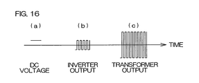
- FIG. 16 shows a waveform at each part of the high frequency lighting device in FIG. 15 , (a) showing a DC input voltage inputted into an inverter 2, (b) showing a waveform of an output voltage of the inverter 2, that is, a primary-side voltage of the main transformer 31, and (c) showing a waveform of a high-frequency voltage on a secondary side of the main transformer 31.
- the uniform flow circuit 601 includes a plurality of transformers, thereby increasing the size thereof.
- the main transformer 31 occupies the largest portion of the device from the viewpoints of size and price, so that the miniaturization of the main transformer 31 is also desired.
- a fluorescent lamp lighting device includes a polarity switching circuit which outputs a low-frequency driving voltage of a predetermined frequency (f) by switching a polarity at the predetermined frequency (f) on DC input, a plurality of fluorescent lamps of which one ends are connected to an output line of the polarity switching circuit, and a uniform flow circuit formed by a constant current circuit connected to the other ends of the plurality of fluorescent lamps and having a transistor for supplying identical current to the respective fluorescent lamps.
- the uniform flow circuit is formed by a constant current circuit including a transistor, thereby achieving miniaturization of the uniform flow circuit. Therefore, the entire high-frequency AC lighting device can be minimized.
- the uniform flow circuit is formed by a constant current circuit including a transistor, if a driving frequency of a fluorescent lamp is high as in a conventional device, the uniform flow circuit is prone to produce significant losses and to increase heat generation. Therefore, it is preferable that the above-mentioned polarity switching circuit has a frequency (f) as low as possible, which is greater than 0 Hz, but not greater than 10 kHz. More preferably, the frequency (f) is greater than 0 Hz, but not greater than 1 kHz.
- the frequency (f) of the polarity switching circuit is lowered from the conventional frequency, so that the fluorescent lamp lighting device is less affected by stray capacitance between the fluorescent lamp or wiring thereof and the chassis (ground potential).
- the fluorescent lamp can be directly mounted to the chassis of a display device, and the wiring can also be extended.
- the direct mounting of the fluorescent lamp to the chassis thereby achieves reduction in thickness of the display device.
- the extension of the wiring allows a display device having a large screen to be readily manufactured.
- the present invention can provide a fluorescent lamp lighting device having both advantages of DC lighting and the conventional high frequency lighting by performing low frequency lighting as described above.
- the frequency of the above-mentioned polarity switching circuit is set so that a frequency (f1) at the start of lighting a fluorescent lamp is higher than a frequency (f) during the lighting, the fluorescent lamp can be easily turned on. Because it may be difficult to start lighting at a low frequency (f) in some cases, especially under low ambient temperature. Therefore, when the high frequency (f1) is used only at the start of lighting, the fluorescent lamp can be easily turned on even at low temperatures. After the start of lighting, the frequency is switched to the low frequency (f), so that the fluorescent lamp lighting device is not affected by stray capacitance.
- a time (T) for controlling the frequency so as to be higher than the above-mentioned predetermined frequency (f) may be regarded as a time required to start lighting a fluorescent lamp. It is desirable to set the time according to ambient temperature conditions or the like. For example, the time is set in the range of 1 second to 10 seconds.
- a high-frequency voltage superimposing circuit for superimposing a high-frequency voltage having the frequency (f2) higher than the above-mentioned predetermined frequency (f) on the above-mentioned low-frequency driving voltage is further provided in a fluorescent lamp.
- a high-frequency voltage superimposed by the high-frequency voltage superimposing circuit is used to start lighting a fluorescent lamp.
- the fluorescent lamp can be continuously lit using the low-frequency driving voltage outputted from the polarity switching circuit. Even during the lighting, the high-frequency current superimposed by the high-frequency voltage superimposing circuit continues to flow.
- an amplitude of the high-frequency voltage is set smaller than that of the low-frequency driving voltage, the fluorescent lamp lighting device is less affected by stray capacitance between the fluorescent lamp or wiring thereof, and the chassis, which causes no problem.
- the high-frequency voltage superimposing circuit may be turned off to prevent the high-frequency current from being supplied during the lighting.
- a high frequency superimposing transformer having a high frequency power supply connected to a primary side thereof and being capable of taking a high-frequency voltage from a secondary side thereof may be used.
- the use of the high frequency superimposing transformer advantageously enables easy insulation between the fluorescent lamp and the high frequency power supply.
- the secondary-side winding of the above-mentioned high frequency superimposing transformer is connected to one output line of the above-mentioned polarity switching circuit through one capacitor, and is connected to the other output line thereof through another capacitor.
- This allows the high frequency superimposing transformer to be smaller, and balanced lighting can also be achieved using low-frequency driving voltages in the same phase from both ends of each fluorescent lamp. Therefore, uneven luminance can be further prevented.
- An LC resonant circuit having an inductor connected in series and a capacitor connected in parallel may be connected between the above-mentioned polarity switching circuit and the above-mentioned plurality of fluorescent lamps. This enables a high-frequency voltage to be produced from a low-frequency driving voltage by self-excitation.
- a DC power supply circuit for producing the above-mentioned DC input may have a main transformer for converting AC voltage, and a rectifier circuit which rectifies output of the main transformer.
- a desired DC voltage required to turn on a fluorescent lamp can be obtained by setting a turns ratio of the main transformer.
- the above-mentioned rectifier circuit is a voltage doubler rectifier circuit
- voltage can be increased with the voltage doubler rectifier circuit, so that the load of a voltage step-up ratio on the main transformer can be reduced.
- the turns ratio of the main transformer can be reduced, thereby advantageously miniaturizing the main transformer.
- an AC voltage supplied to the above-mentioned main transformer is produced by an inverter which obtains a high frequency output having a predetermined frequency from DC.
- the high frequency generated by the inverter can be made high to advantageously improve conversion efficiency of the main transformer.
- the main transformer can be miniaturized.
- the higher the frequency thereof becomes the larger the effect of stray capacitance between the fluorescent lamp and the chassis becomes.
- the wiring distance cannot be extended, thereby limiting the arrangement of fluorescent lamps in the device.
- wattless current becomes larger, illumination of fluorescent lamps falls, and uniform display luminance becomes difficult to achieve.
- the frequency of the inverter has not yet been able to be increased to a frequency suitable for the main transformer.
- a high frequency output from an inverter is once rectified to DC by a rectifier circuit, and is then supplied to a fluorescent lamp via a polarity switching circuit. That is, the frequency of the inverter and the driving frequency of the fluorescent lamp can be separately set up. Therefore, the frequency of the inverter can be made sufficiently high so that the conversion efficiency of the main transformer can be advantageously improved. This facilitates miniaturization of the main transformer, and at the same time, the driving frequency f of the fluorescent lamp can be lowered as described above. Thus, the fluorescent lamp and wiring thereof are no longer affected by stray capacitance.
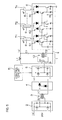
- FIG. 1 is a circuit diagram of a fluorescent lamp lighting device according to the present invention.
- the lighting device includes an inverter 2 which converts DC input into AC, a main transformer 3 which increases AC voltage from the inverter 2, a voltage doubler rectifier circuit 4 which doubles and rectifies the AC voltage outputted from the main transformer 3, a polarity switching circuit 5 which switches the polarity of the rectified DC voltage, a plurality (n pieces) of cold cathode fluorescent tubes 71, ..., 7n connected to output lines (e), (f) of the polarity switching circuit 5, and a uniform flow circuit 6 connected to the other ends of the above-mentioned plurality of cold cathode fluorescent tubes (71, ..., 7n), for supplying identical current to the respective cold cathode fluorescent tubes (71, ..., 7n).
- a DC input is first converted into an AC frequency suitable for the main transformer 3 by switching a switching transistor included in an inverter 2.
- the "AC frequency suitable for the main transformer 3" refers to a frequency at which the main transformer 3 can obtain sufficient conversion efficiency, that is usually in the range of several tens of kHz to several hundreds of kHz.
- the main transformer 3 needs to be increased in size, and thus the entire device becomes larger and heavier.
- the frequency is higher than this range, the effect of parallel capacitance generated within the main transformer 3 is increased, so that resonance occurs to reduce the conversion efficiency.
- the above-mentioned AC voltage is increased at a predetermined voltage step-up ratio by the main transformer 3 having a predetermined number of turns and a number of turns ratio. Further, the voltage doubler rectifier circuit 4 performs rectification and voltage step-up. As a result of this, DC voltage required to turn on the cold cathode fluorescent tubes (71, ..., 7n) can be obtained.
- the "DC voltage required to turn on the cold cathode fluorescent tubes (71, ..., 7n)" is on the order of 1000 V to 2000 V.
- the DC voltage is converted into AC voltage by turning on/off the switching transistor in the polarity switching circuit 5.
- a control circuit 51 is used to control the turning on/off of the switching transistor.
- the control circuit 51 supplies an on/off signal to a gate of each switching transistor, thereby controlling the turning on/off of each of the switching transistors.
- a frequency f of the on/off signal may be in the range of greater than 0 Hz but not greater than 20 kHz.
- the frequency f is preferably greater than 0 Hz but not greater than 10 kHz, or more preferably greater than 0 Hz but not greater than 1 kHz.
- the uniform flow circuit 6 includes electronic circuits (referred to as constant current circuits) 61, ..., 6n which obtain constant current by using electric current flowing through between a collector and an emitter of a transistor, and the number of the electronic circuits correspond to the number of the cold cathode fluorescent tubes (71, ..., 7n).
- the cold cathode fluorescent tubes (71, ..., 7n) and the constant current circuits (61, ..., 6n) are connected in series to each other, respectively.
- the series circuits (the number thereof is equal to the number of cold cathode fluorescent tubes (71, ..., 7n)) of the cold cathode fluorescent tubes (71, ..., 7n) and the constant current circuits (61, ..., 6n) are connected to two output lines (e), (f) of the polarity switching circuit 5.
- transistors of NPN type and PNP type are connected in parallel with each other in the respective constant current circuits (61, ..., 6n).
- a resistance R is connected between an emitter and a ground.
- a base of the transistor is commonly connected to the respective transistors.
- a voltage at this common base is indicated as Vb. Since a voltage across the resistance R is substantially equal to the voltage Vb, and the voltage Vb is commonly applied to the respective transistors, the voltage across the resistance R is substantially equal in each of the constant current circuits (61, ..., 6n). Therefore, electric currents flowing through the respective constant current circuits in one direction (a direction from the collector to the emitter of the NPN transistor) are substantially equal, whereby constant current can be obtained. Electric currents flowing in the reverse direction (a direction from the emitter to the collector of the PNP transistor) are also equalized by the same action of the PNP transistor, whereby constant current can be obtained.
- constant current is realized using the constant current circuits (61, ..., 6n) having the transistors, so that miniaturization and weight reduction can be realized as compared to the uniform flow circuit 601 conventionally utilizing a plurality of transformers.
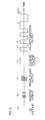
- FIG. 2 is a graph showing a waveform at each part of the lighting device of FIG. 1 .
- FIG. 2 (a) shows a DC input voltage to be inputted into the inverter 2
- FIG. 2 (b) shows a waveform of an output voltage of the inverter 2, that is, a primary-side voltage of the main transformer
- FIG. 2 (c) shows a waveform of a secondary-side voltage of the main transformer 3.
- the secondary-side voltage of the main transformer 3 is increased with respect to the primary-side voltage thereof, according to the number of turns ratio of the main transformer 3.
- FIG. 2 (d) shows an output waveform of the voltage doubler rectifier circuit 4. This output voltage is more increased than the secondary-side voltage of the main transformer 3, and is also rectified into pulsating current.
- FIG. 2 (e) shows an output waveform of the polarity switching circuit 5.
- a DC output rectified into the pulsating current is switched by the polarity switching circuit 5 so as to alternately become positive and negative.
- the output current thus switched is supplied to the respective cold cathode fluorescent tubes (71, ..., 7n) through the uniform flow circuit 6.
- the switching frequency of the polarity switching circuit 5 is set faster only at the start of lighting, and the details thereof will be described below. Although it has been described above that the switching frequency f of the polarity switching circuit 5 is in the range of greater than 0 Hz but not greater than 20 kHz, it may be set to an even faster frequency f1 (f1 ⁇ f) only at the start of lighting, and then switched to a slower frequency f within the range of greater than 0 Hz but not greater than 20 kHz after the lighting-up.
- FIG. 2 (e) shows an example in which an on/off frequency of the control circuit 51 is set to the faster frequency f1 only at the start of lighting, and is then switched to the slower frequency f after the lighting-up.
- FIG. 3 is a graph showing a relationship between time and frequency, in which the frequency is set to the faster frequency f1 only at a start of lighting and is then switched to the slow frequency f after a predetermined period of time T passes.
- f1 1 kHz
- f 120 Hz which is slower than the above.
- the predetermined time T is set according to ambient temperature, and is set in the range of about 1 second to 10 seconds at normal temperature. Under low temperature environment in which lighting hardly starts, the predetermined time T is set longer, while under high temperature environment, the predetermined time T is set shorter.
- the faster frequency f1 may be set only at the start of lighting, and as the predetermined time T passes from the start, the frequency f1 may be gradually lowered to converge on the frequency f.
- the setting range of the predetermined time T is generally the same as that in the case of FIG. 3 .
- the start of lighting of the cold cathode fluorescent tubes (71, ..., 7n) can be facilitated using stray capacitance between the cold cathode fluorescent tubes (71, ..., 7n) and wiring connected thereto, and a chassis 8 that supports the cold cathode fluorescent tubes (71, ..., 7n).
- the plurality of cold cathode fluorescent tubes (71, ..., 7n) can be turned on at a low frequency with the frequency f.
- the low frequency f is in the range of greater than 0 Hz but not greater than 20 kHz. Preferably, it ranges greater than 0 Hz but not greater than 10 kHz, or more preferably greater than 0 Hz but not greater than 1 kHz.
- the cold cathode fluorescent tubes (71, ..., 7n) have been turned on by supplying high frequency current of several tens kHz thereto with the inverter 2.
- the cold cathode fluorescent tubes (71, ..., 7n) are now turned on with electric current having such low frequency f. Therefore, the effect of stray capacitance generated between the cold cathode fluorescent tubes (71, ..., 7n) and the chassis 8 and between wiring connected thereto and the chassis 8 can be reduced, thereby enabling uniformity of screen luminance to be nearly ideal.
- the main transformer 3 can be driven at a high frequency independent of the switching frequency f of the polarity switching circuit 5, the size of the main transformer 3 can be made smaller.
- the lighting device of the present invention is used for backlights of liquid crystal display devices, the entire lighting device can be minimized. Moreover, since the effect of stray capacitance can be reduced by turning on the cold cathode fluorescent tubes with a low frequency, the cold cathode fluorescent tubes and the chassis supporting them can be brought as close as possible to each other without limitation. Thus, the thickness of the liquid crystal display device can be made thinner.
- the voltage having the frequency f2 is superimposed on the voltage having the frequency f.
- FIG. 5 is a circuit diagram of a fluorescent lamp lighting device in which an inductor L1, a capacitor C1, a high frequency power supply 9, and a voltage superimposing transformer 12 are provided between the polarity switching circuit 5 and the plurality of cold cathode fluorescent tubes (71, ..., 7n). These inductor L1, capacitor C1, high frequency power supply 9, and voltage superimposing transformer 12 form a high-frequency voltage superimposing circuit 1.
- the inductor L1 is connected in series between the polarity switching circuit 5 and the cold cathode tubes (71, ..., 7n), and prevents backflow of a superimposed high frequency current into the polarity switching circuit 5.
- the capacitor C1 is provided in order to prevent short circuit of a low-frequency driving voltage.
- the voltage superimposing transformer 12 is composed of a primary-side winding T1 and a secondary-side winding T2, and the high frequency power supply 9 is connected to the primary-side winding T1.
- FIG. 6A shows an output voltage waveform of the polarity switching circuit 5. This waveform, which is the same as in FIG. 2 (e) , is drawn without the pulsating current omitted.
- FIG. 6B shows an output voltage waveform in which a high-frequency voltage having the frequency f2 is superimposed by the high-frequency voltage superimposing circuit 1.
- b is desirably on the order of 0.1 to 0.5 times of a. If b is lower than 0.1 times of a, the effect of superimposing the high frequency f2 becomes small, leading to generally the same result as the case of starting lighting only at the low frequency f. If b is higher than 0.5 times of a, the stray capacitance affects to increase power loss during the lighting.
- the high-frequency voltage is used to turn on the cold cathode fluorescent tubes (71, ..., 7n), so that the lighting can be readily started. Especially, it is effective at the start of lighting at low temperatures.
- the brightness of the cold cathode fluorescent tubes (71, ..., 7n) during the lighting can be controlled by adjusting the amplitude "b" of the high-frequency voltage of the frequency f2.
- the brightness of the cold cathode fluorescent tubes (71, ..., 7n) during the lighting can be adjusted by selecting a value of the frequency f2. That is, when there is a leakage magnetic flux from the secondary-side winding T2 in the voltage superimposing transformer 12, higher frequency f2 allows the cold cathode fluorescent tubes (71, ..., 7n) to be dimmed, and lower frequency f2 allows the cold cathode fluorescent tubes (71, ..., 7n) to be brighter.
- higher frequency f2 allows the cold cathode fluorescent tubes (71, ..., 7n) to be brighter, and lower frequency f2 allows the cold cathode fluorescent tubes (71, ..., 7n) to be dimmed.
- FIG. 7 is a concrete circuit diagram of the high frequency power supply 9 described above.
- the high frequency power supply 9 is a circuit connecting two transistors Q1, Q2 in series, in which an AC switching circuit 11 which alternately outputs high/low voltages at the frequency f2 is connected to the base of the transistors Q1, Q2. While the AC switching circuit 11 is outputting a high voltage, the transistor Q1 is turned on and an electric current is charged to the primary-side coil T1 through a capacitor C3 from the power supply F. While the AC switching circuit 11 is outputting a low voltage, the transistor Q2 is turned on and the electric current thus charged to the primary-side coil T1 discharges the capacitor C3. Thus, a high frequency current can be supplied to the primary-side coil T1.
- FIG. 8 a transformer having the secondary-side winding T2 with a tap is used as the voltage superimposing transformer 12, and the output line (e) from the polarity switching circuit 5 is connected to this tap.
- FIG. 8 is a diagram showing the following circuit arrangement: A plurality of cold cathode fluorescent tubes are divided into two groups, the cold cathode fluorescent tubes in each group are connected in parallel, and the connecting ends of the cold cathode fluorescent tubes are connected to both ends (g), (h) of the secondary-side winding T2, respectively.
- Cold cathode fluorescent tubes in one group are denoted as 71, 72, ..., and those in the other group are denoted as 81, 82, ....
- FIG. 8 A plurality of cold cathode fluorescent tubes are divided into two groups, the cold cathode fluorescent tubes in each group are connected in parallel, and the connecting ends of the cold cathode fluorescent tubes are connected to both ends (g), (h) of the secondary-side winding T2, respectively.
- the high frequency power supply 9 is connected to the primary-side coil T1 in the voltage superimposing transformer 12.
- the frequency f2 of the high frequency power supply 9 is set to a frequency on the order of 5 to 50 times of the above-mentioned low frequency f.
- a low-frequency voltage outputted from the polarity switching circuit 5 is divided at the tap and is then applied from both the ends (g), (h) of the secondary-side winding T2 to the respective groups, thereby turning on and driving the cold cathode fluorescent tubes in each group.
- the low-frequency voltage outputted from the polarity switching circuit 5 is in the same phase at both the ends (g), (h) of the secondary-side winding T2.
- a high-frequency voltage outputted from the high frequency power supply 9 is applied in the opposite phase from both the ends of the secondary-side winding T2 to start lighting the cold cathode fluorescent tubes in each group.
- the high-frequency voltage outputted from the high frequency power supply 9 is in the opposite phase at both the ends (g), (h) of the secondary-side winding T2.
- the capacitor C1 as seen in the circuit of FIG. 5 is no longer required.
- the secondary-side winding T2 having the center tap is used, the DC magnetization of the core is offset. Therefore, core saturation is less likely to occur, thereby allowing to use a small transformer with a small core.
- FIG. 9 shows an example of a circuit in which the capacitors C1, C2 connected in series with each other are connected to output lines from the polarity switching circuit 5, the voltage superimposing transformer 12 is connected to an intermediate junction (i) between the capacitors C1 and C2, and a high-frequency voltage for the start of lighting is supplied from the voltage superimposing transformer 12 to the cold cathode fluorescent tubes (71, ..., 7n) through the capacitors C1, C2.
- the high-frequency voltage outputted from the high frequency power supply 9 is applied from the secondary-side winding T2 through the capacitors C1, C2 to start lighting each of the cold cathode fluorescent tubes (71, ..., 7n).
- the high-frequency voltage superimposing circuit 1 described in FIGS. 5 to 9 is a separate-excitation type circuit using the high frequency power supply 9.
- a self-excitation type circuit in which a resonant circuit having a capacitor C and an inductor L is provided on both lines (e), (f) on the output side of the polarity switching circuit 5 to oscillate a high-frequency voltage can also be adopted.
- FIG. 10 is a circuit diagram of a fluorescent lamp lighting device using a self-excitation type high-frequency voltage superimposing circuit 1'.
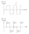
- FIG. 11A shows an output voltage waveform of the polarity switching circuit 5 in the case where an LC resonant circuit does not exist. This waveform is the same as that in FIG. 6A .
- FIG. 11B shows an output voltage waveform obtained after a high-frequency voltage is superimposed by the LC resonant circuit.
- the LC resonant circuit causes an oscillation output to appear at the time when an low frequency output waveform is switched from negative to positive or from positive to negative, and the oscillation output gradually decreases.
- the high-frequency voltage is superimposed on the output voltage waveform of the polarity switching circuit 5, the high-frequency voltage is used to turn on the cold cathode fluorescent tubes (71, ..., 7n), so that the lighting can be readily started.
- the above-mentioned capacitor C may be constituted by a stray capacitance between the cold cathode fluorescent tubes (71, ..., 7n) and the chassis 8 and between wiring connected thereto and the chassis 8.
- FIG. 12 is a circuit diagram of a major portion of a transformerless lighting device from which a main transformer 3 is omitted.
- AC voltage is directly obtained by a resonant circuit 2' using a coil and a transistor, with respect to DC input.
- the AC voltage obtained by the resonant circuit is on the order of 10 times of the DC input, for example, 240 V, and has a frequency of 200 kHz.
- a predetermined voltage for example a DC voltage of 1500 V, is obtained by letting the AC voltage pass through the voltage doubler rectifier circuit 4.
- An arrangement subsequent to the voltage doubler rectifier circuit 4 is the same as those shown in FIGS. 1 to 10 .
- the main transformer 3 can be eliminated, so that the lighting device can be further miniaturized.
- FIG. 13 is a circuit diagram of a major portion showing an arrangement in which an inverter circuit 2 and a main transformer 3 of an apparatus (e.g., television receiver) 10, in which the lighting device is incorporated, are used and the above-described inverter circuit 2 and main transformer 3 are omitted.
- An AC voltage is obtained from a secondary-side winding of a power supply transformer in the apparatus 10, and then passes through the voltage doubler rectifier circuit 4 to perform voltage step-up and rectification.
- the inverter 2 and the transformer both dedicated to the cold cathode fluorescent tubes (71, ..., 7n) are no longer required. Thus, the entire device can be minimized.
- FIG. 14 is a circuit diagram showing another example of a uniform flow circuit.
- a circuit 6a sending constant current in one direction and a circuit 6b sending it in the other direction are separated from each other and installed on respective sides of the cold cathode fluorescent tubes.
- the operation of the constant current circuits 6a, 6b is the same as that described using FIG. 1 .
- This uniform flow circuit allows use of NPN transistors only, which is advantageously cost effective.
Landscapes
- Engineering & Computer Science (AREA)
- Power Engineering (AREA)
- Circuit Arrangements For Discharge Lamps (AREA)
- Dc-Dc Converters (AREA)
- Control Of Indicators Other Than Cathode Ray Tubes (AREA)
Abstract
A fluorescent lamp lighting device includes: a polarity switching circuit (5) for performing polarity switching with a low frequency (f) not greater than 20 kHz on DC input; a plurality of fluorescent lamps (71, ..., 7n) connected to the output line of the polarity switching circuit (5); a uniform flow circuit (6) formed by constant current circuits (61, ..., 6n) connected to the other end of the fluorescent lamps (71, ..., 7n) and having a transistor for supplying identical current to the respective fluorescent lamps (71, ..., 7n). Since the fluorescent lamps are turned on with the low frequency (f) not greater than 20 kHz, they are hardly affected by stray capacitance, the fluorescent lamps (71, ..., 7n) can be arranged near a chassis (8) of a display device and it is possible to prolong wiring. (FIG. 1 )
Description
- The present invention relates to a fluorescent lamp lighting device capable of simultaneously turning on a plurality of fluorescent lamps.
- A type of fluorescent lamp called a cold cathode fluorescent tube is used for backlights of various display devices, such as a liquid crystal display. Conventionally, a high-frequency AC lighting system using an inverter has been adopted to turn on and drive the cold cathode fluorescent tube.
-
FIG. 15 is a circuit diagram showing a conventional high-frequency AC lighting device. The high-frequency AC lighting device comprises aninverter circuit 21 for supplying high-frequency AC power source of several tens kHz, amain transformer 31, a plurality of cold cathodefluorescent tubes 70 of which one ends are connected to an output line of themain transformer 31, and auniform flow circuit 601 composed of a plurality of transformers, connected to the other ends of the above-mentioned plurality of cold cathodefluorescent tubes 70, for supplying uniform current to the respective cold cathodefluorescent tubes 70. -
FIG. 16 shows a waveform at each part of the high frequency lighting device inFIG. 15 , (a) showing a DC input voltage inputted into aninverter 2, (b) showing a waveform of an output voltage of theinverter 2, that is, a primary-side voltage of themain transformer 31, and (c) showing a waveform of a high-frequency voltage on a secondary side of themain transformer 31. - Patent Publication 1: Japanese Unexamined Patent Publication No.
2000-294391 - In such high frequency lighting device, the
uniform flow circuit 601 includes a plurality of transformers, thereby increasing the size thereof. - In the conventional high-frequency AC lighting device, the
main transformer 31 occupies the largest portion of the device from the viewpoints of size and price, so that the miniaturization of themain transformer 31 is also desired. - There also arises a problem that since stray capacitance exists between a fluorescent lamp and a chassis and the like therearound, when the fluorescent lamp is turned on with a high-frequency AC power supply at several tens of kHz, a high frequency current flows into the chassis through the stray capacitance, thereby reducing efficiency during lighting.
- It is an object of the present invention to provide a fluorescent lamp lighting device capable of using a small uniform flow circuit, effectively turning on a fluorescent lamp, and generally miniaturizing its size.
- According to the present invention, a fluorescent lamp lighting device includes a polarity switching circuit which outputs a low-frequency driving voltage of a predetermined frequency (f) by switching a polarity at the predetermined frequency (f) on DC input, a plurality of fluorescent lamps of which one ends are connected to an output line of the polarity switching circuit, and a uniform flow circuit formed by a constant current circuit connected to the other ends of the plurality of fluorescent lamps and having a transistor for supplying identical current to the respective fluorescent lamps.
- With the fluorescent lamp lighting device, the uniform flow circuit is formed by a constant current circuit including a transistor, thereby achieving miniaturization of the uniform flow circuit. Therefore, the entire high-frequency AC lighting device can be minimized.
- Since the uniform flow circuit is formed by a constant current circuit including a transistor, if a driving frequency of a fluorescent lamp is high as in a conventional device, the uniform flow circuit is prone to produce significant losses and to increase heat generation. Therefore, it is preferable that the above-mentioned polarity switching circuit has a frequency (f) as low as possible, which is greater than 0 Hz, but not greater than 10 kHz. More preferably, the frequency (f) is greater than 0 Hz, but not greater than 1 kHz.
- As described above, the frequency (f) of the polarity switching circuit is lowered from the conventional frequency, so that the fluorescent lamp lighting device is less affected by stray capacitance between the fluorescent lamp or wiring thereof and the chassis (ground potential). For this reason, the fluorescent lamp can be directly mounted to the chassis of a display device, and the wiring can also be extended. The direct mounting of the fluorescent lamp to the chassis thereby achieves reduction in thickness of the display device. The extension of the wiring allows a display device having a large screen to be readily manufactured.
- Conventionally, DC (0 Hz) lighting has been tried with a fluorescent lamp. Such DC lighting can eliminate the effect of stray capacitance. However, when a fluorescent lamp is turned on with DC, "cataphoresis phenomenon or dark end effect" occurs in which mercury in the fluorescent lamp moves by an electric field, thereby causing the near-by portion of the anode to darken with time. Further, "sputter phenomenon" also occurs in which only one of the electrodes is worn. Hence, screen luminance cannot be uniform.
- Therefore, the present invention can provide a fluorescent lamp lighting device having both advantages of DC lighting and the conventional high frequency lighting by performing low frequency lighting as described above.
- When the frequency of the above-mentioned polarity switching circuit is set so that a frequency (f1) at the start of lighting a fluorescent lamp is higher than a frequency (f) during the lighting, the fluorescent lamp can be easily turned on. Because it may be difficult to start lighting at a low frequency (f) in some cases, especially under low ambient temperature. Therefore, when the high frequency (f1) is used only at the start of lighting, the fluorescent lamp can be easily turned on even at low temperatures. After the start of lighting, the frequency is switched to the low frequency (f), so that the fluorescent lamp lighting device is not affected by stray capacitance.
- A time (T) for controlling the frequency so as to be higher than the above-mentioned predetermined frequency (f) may be regarded as a time required to start lighting a fluorescent lamp. It is desirable to set the time according to ambient temperature conditions or the like. For example, the time is set in the range of 1 second to 10 seconds.
- Alternatively, an arrangement in which the frequency (f) is not switched, but in which a high-frequency voltage having a higher frequency (f2) is superimposed on a low-frequency driving voltage may be adopted. More specifically, a high-frequency voltage superimposing circuit for superimposing a high-frequency voltage having the frequency (f2) higher than the above-mentioned predetermined frequency (f) on the above-mentioned low-frequency driving voltage is further provided in a fluorescent lamp.
- With this arrangement, a high-frequency voltage superimposed by the high-frequency voltage superimposing circuit is used to start lighting a fluorescent lamp. After the start of lighting, the fluorescent lamp can be continuously lit using the low-frequency driving voltage outputted from the polarity switching circuit. Even during the lighting, the high-frequency current superimposed by the high-frequency voltage superimposing circuit continues to flow. However, if an amplitude of the high-frequency voltage is set smaller than that of the low-frequency driving voltage, the fluorescent lamp lighting device is less affected by stray capacitance between the fluorescent lamp or wiring thereof, and the chassis, which causes no problem. Of course, the high-frequency voltage superimposing circuit may be turned off to prevent the high-frequency current from being supplied during the lighting.
- As the above-mentioned high-frequency voltage superimposing circuit, a high frequency superimposing transformer having a high frequency power supply connected to a primary side thereof and being capable of taking a high-frequency voltage from a secondary side thereof may be used. The use of the high frequency superimposing transformer advantageously enables easy insulation between the fluorescent lamp and the high frequency power supply.
- There may be an arrangement in which a center tap is provided on a secondary-side winding of the above-mentioned high frequency superimposing transformer, an output line of the above-mentioned polarity switching circuit is connected to the center tap, the above-mentioned plurality of fluorescent lamps are divided into two groups, and one ends of the fluorescent lamps belonging to each group are connected to each ends of the above-mentioned secondary-side winding. This allows the high frequency superimposing transformer to be made even smaller.
- There may also be an arrangement in which the secondary-side winding of the above-mentioned high frequency superimposing transformer is connected to one output line of the above-mentioned polarity switching circuit through one capacitor, and is connected to the other output line thereof through another capacitor. This allows the high frequency superimposing transformer to be smaller, and balanced lighting can also be achieved using low-frequency driving voltages in the same phase from both ends of each fluorescent lamp. Therefore, uneven luminance can be further prevented.
- An LC resonant circuit having an inductor connected in series and a capacitor connected in parallel may be connected between the above-mentioned polarity switching circuit and the above-mentioned plurality of fluorescent lamps. This enables a high-frequency voltage to be produced from a low-frequency driving voltage by self-excitation.
- A DC power supply circuit for producing the above-mentioned DC input may have a main transformer for converting AC voltage, and a rectifier circuit which rectifies output of the main transformer. A desired DC voltage required to turn on a fluorescent lamp can be obtained by setting a turns ratio of the main transformer.
- If the above-mentioned rectifier circuit is a voltage doubler rectifier circuit, voltage can be increased with the voltage doubler rectifier circuit, so that the load of a voltage step-up ratio on the main transformer can be reduced. Thus, the turns ratio of the main transformer can be reduced, thereby advantageously miniaturizing the main transformer.
- It is preferable that an AC voltage supplied to the above-mentioned main transformer is produced by an inverter which obtains a high frequency output having a predetermined frequency from DC. Thus, the high frequency generated by the inverter can be made high to advantageously improve conversion efficiency of the main transformer. In general, the higher the frequency is, the more the conversion efficiency of the transformer increases. This reduces the number of turns in the main transformer, thereby allowing the size of the main transformer to be sufficiently small.
- In the conventional high-frequency AC lighting device shown in
FIG. 15 , as the frequency of the inverter increases, the main transformer can be miniaturized. However, the higher the frequency thereof becomes, the larger the effect of stray capacitance between the fluorescent lamp and the chassis becomes. When the stray capacitance is larger, the wiring distance cannot be extended, thereby limiting the arrangement of fluorescent lamps in the device. Further, wattless current becomes larger, illumination of fluorescent lamps falls, and uniform display luminance becomes difficult to achieve. - Thus, the frequency of the inverter has not yet been able to be increased to a frequency suitable for the main transformer.
- However, according to the present invention, a high frequency output from an inverter is once rectified to DC by a rectifier circuit, and is then supplied to a fluorescent lamp via a polarity switching circuit. That is, the frequency of the inverter and the driving frequency of the fluorescent lamp can be separately set up. Therefore, the frequency of the inverter can be made sufficiently high so that the conversion efficiency of the main transformer can be advantageously improved. This facilitates miniaturization of the main transformer, and at the same time, the driving frequency f of the fluorescent lamp can be lowered as described above. Thus, the fluorescent lamp and wiring thereof are no longer affected by stray capacitance.
- These and other features, advantages and effects of the present invention will be more fully apparent from the following detailed description set forth below when taken in conjunction with the accompanying drawings.
-
-
FIG. 1 is a circuit diagram of a fluorescent lamp lighting device according to the present invention; -
FIG. 2 is a graph showing a waveform at each part of the lighting device ofFIG. 1 ; -
FIG. 3 is a graph showing that a faster frequency f1 is set only at a start of lighting a fluorescent lamp and is then switched to a slower frequency f after the lighting-up; -
FIG. 4 is a graph showing that a faster frequency f1 is set only at a start of lighting a fluorescent lamp and is then switched to a slower frequency f after the lighting-up; -
FIG. 5 is a circuit diagram of a fluorescent lamp lighting device according to the present invention, in which a high-frequency voltage superimposing circuit is provided between apolarity switching circuit 5 and a plurality of cold cathode fluorescent tubes (71, ..., 7n); -
FIG. 6A is a waveform chart showing an output voltage waveform of thepolarity switching circuit 5; -
FIG. 6B is a waveform chart showing an output voltage waveform obtained after a high-frequency voltage is superimposed by the high-frequency voltage superimposing circuit; -
FIG. 7 is a concrete circuit diagram of a highfrequency power supply 9 two transistors Q1, Q2; -
FIG. 8 is a circuit diagram of a fluorescent lamp lighting device according to the present invention, comprising a high-frequency voltage superimposing circuit according to a variation; -
FIG. 9 is a circuit diagram of a fluorescent lamp lighting device according to the present invention, further comprising a high-frequency voltage superimposing circuit according to another variation; -
FIG. 10 is a circuit diagram of a fluorescent lamp lighting device using a self-excitation type high-frequency voltage superimposing circuit; -
FIG. 11A is a chart showing an output voltage waveform of thepolarity switching circuit 5; -
FIG. 11B is a chart showing an output voltage waveform obtained after a high-frequency voltage is superimposed; -
FIG. 12 is a circuit diagram of a major portion of a transformerless lighting device, from which amain transformer 3 is omitted; -
FIG. 13 is a circuit diagram of a major portion showing an arrangement in which an inverter circuit and a transformer of adevice 10 in which the lighting device is incorporated remain in use, from which aninverter circuit 2 and amain transformer 3 are omitted; -
FIG. 14 is a circuit diagram showing another example of a uniform flow circuit; -
FIG. 15 is a circuit diagram showing a conventional high-frequency AC lighting device; and -
FIG. 16 is a graph showing a waveform at each part of the high frequency lighting device ofFIG. 15 . -
- 1, 1'
- High-frequency voltage superimposing circuit
- 2
- Inverter
- 3
- Main transformer
- 4
- Voltage doubler rectifier circuit
- 5
- Polarity switching circuit
- 6
- Uniform flow circuit
- 61, ..., 6n
- Constant current circuits
- 71, ..., 7n
- Cold cathode tubes
- 8
- Chassis
- 9
- High frequency power supply
- 10
- Apparatus
- 12
- Voltage superimposing transformer
- 51
- Control circuit
- The embodiments of the present invention will be described in detail below while referring to the accompanying drawings.
-
FIG. 1 is a circuit diagram of a fluorescent lamp lighting device according to the present invention. - The lighting device includes an
inverter 2 which converts DC input into AC, amain transformer 3 which increases AC voltage from theinverter 2, a voltagedoubler rectifier circuit 4 which doubles and rectifies the AC voltage outputted from themain transformer 3, apolarity switching circuit 5 which switches the polarity of the rectified DC voltage, a plurality (n pieces) of coldcathode fluorescent tubes 71, ..., 7n connected to output lines (e), (f) of thepolarity switching circuit 5, and auniform flow circuit 6 connected to the other ends of the above-mentioned plurality of cold cathode fluorescent tubes (71, ..., 7n), for supplying identical current to the respective cold cathode fluorescent tubes (71, ..., 7n). - The operation of the device will be described. A DC input is first converted into an AC frequency suitable for the
main transformer 3 by switching a switching transistor included in aninverter 2. The "AC frequency suitable for themain transformer 3" refers to a frequency at which themain transformer 3 can obtain sufficient conversion efficiency, that is usually in the range of several tens of kHz to several hundreds of kHz. When the frequency is excessively lower than this range, themain transformer 3 needs to be increased in size, and thus the entire device becomes larger and heavier. When the frequency is higher than this range, the effect of parallel capacitance generated within themain transformer 3 is increased, so that resonance occurs to reduce the conversion efficiency. - Next, the above-mentioned AC voltage is increased at a predetermined voltage step-up ratio by the
main transformer 3 having a predetermined number of turns and a number of turns ratio. Further, the voltagedoubler rectifier circuit 4 performs rectification and voltage step-up. As a result of this, DC voltage required to turn on the cold cathode fluorescent tubes (71, ..., 7n) can be obtained. The "DC voltage required to turn on the cold cathode fluorescent tubes (71, ..., 7n)" is on the order of 1000 V to 2000 V. - The DC voltage is converted into AC voltage by turning on/off the switching transistor in the
polarity switching circuit 5. Acontrol circuit 51 is used to control the turning on/off of the switching transistor. Thecontrol circuit 51 supplies an on/off signal to a gate of each switching transistor, thereby controlling the turning on/off of each of the switching transistors. - A frequency f of the on/off signal may be in the range of greater than 0 Hz but not greater than 20 kHz. The frequency f is preferably greater than 0 Hz but not greater than 10 kHz, or more preferably greater than 0 Hz but not greater than 1 kHz.
- The
uniform flow circuit 6 includes electronic circuits (referred to as constant current circuits) 61, ..., 6n which obtain constant current by using electric current flowing through between a collector and an emitter of a transistor, and the number of the electronic circuits correspond to the number of the cold cathode fluorescent tubes (71, ..., 7n). The cold cathode fluorescent tubes (71, ..., 7n) and the constant current circuits (61, ..., 6n) are connected in series to each other, respectively. The series circuits (the number thereof is equal to the number of cold cathode fluorescent tubes (71, ..., 7n)) of the cold cathode fluorescent tubes (71, ..., 7n) and the constant current circuits (61, ..., 6n) are connected to two output lines (e), (f) of thepolarity switching circuit 5. - As shown in
FIG. 1 , transistors of NPN type and PNP type are connected in parallel with each other in the respective constant current circuits (61, ..., 6n). As for the NPN transistor, a resistance R is connected between an emitter and a ground. A base of the transistor is commonly connected to the respective transistors. A voltage at this common base is indicated as Vb. Since a voltage across the resistance R is substantially equal to the voltage Vb, and the voltage Vb is commonly applied to the respective transistors, the voltage across the resistance R is substantially equal in each of the constant current circuits (61, ..., 6n). Therefore, electric currents flowing through the respective constant current circuits in one direction (a direction from the collector to the emitter of the NPN transistor) are substantially equal, whereby constant current can be obtained. Electric currents flowing in the reverse direction (a direction from the emitter to the collector of the PNP transistor) are also equalized by the same action of the PNP transistor, whereby constant current can be obtained. - Thus, constant current is realized using the constant current circuits (61, ..., 6n) having the transistors, so that miniaturization and weight reduction can be realized as compared to the
uniform flow circuit 601 conventionally utilizing a plurality of transformers. -
FIG. 2 is a graph showing a waveform at each part of the lighting device ofFIG. 1 . -
FIG. 2 (a) shows a DC input voltage to be inputted into theinverter 2,FIG. 2 (b) shows a waveform of an output voltage of theinverter 2, that is, a primary-side voltage of the main transformer, andFIG. 2 (c) shows a waveform of a secondary-side voltage of themain transformer 3. The secondary-side voltage of themain transformer 3 is increased with respect to the primary-side voltage thereof, according to the number of turns ratio of themain transformer 3.FIG. 2 (d) shows an output waveform of the voltagedoubler rectifier circuit 4. This output voltage is more increased than the secondary-side voltage of themain transformer 3, and is also rectified into pulsating current.FIG. 2 (e) shows an output waveform of thepolarity switching circuit 5. A DC output rectified into the pulsating current is switched by thepolarity switching circuit 5 so as to alternately become positive and negative. The output current thus switched is supplied to the respective cold cathode fluorescent tubes (71, ..., 7n) through theuniform flow circuit 6. - It is preferable that the switching frequency of the
polarity switching circuit 5 is set faster only at the start of lighting, and the details thereof will be described below. Although it has been described above that the switching frequency f of thepolarity switching circuit 5 is in the range of greater than 0 Hz but not greater than 20 kHz, it may be set to an even faster frequency f1 (f1≥f) only at the start of lighting, and then switched to a slower frequency f within the range of greater than 0 Hz but not greater than 20 kHz after the lighting-up. -
FIG. 2 (e) shows an example in which an on/off frequency of thecontrol circuit 51 is set to the faster frequency f1 only at the start of lighting, and is then switched to the slower frequency f after the lighting-up. -
FIG. 3 is a graph showing a relationship between time and frequency, in which the frequency is set to the faster frequency f1 only at a start of lighting and is then switched to the slow frequency f after a predetermined period of time T passes. For example, at the start of lighting, f1 = 1 kHz, and after the lighting-up, f = 120 Hz which is slower than the above. The predetermined time T is set according to ambient temperature, and is set in the range of about 1 second to 10 seconds at normal temperature. Under low temperature environment in which lighting hardly starts, the predetermined time T is set longer, while under high temperature environment, the predetermined time T is set shorter. - As shown in
FIG. 4 , the faster frequency f1 may be set only at the start of lighting, and as the predetermined time T passes from the start, the frequency f1 may be gradually lowered to converge on the frequency f. The setting range of the predetermined time T is generally the same as that in the case ofFIG. 3 . - In this manner, when the switching frequency of the
polarity switching circuit 5 is increased only at the start of lighting, the start of lighting of the cold cathode fluorescent tubes (71, ..., 7n) can be facilitated using stray capacitance between the cold cathode fluorescent tubes (71, ..., 7n) and wiring connected thereto, and achassis 8 that supports the cold cathode fluorescent tubes (71, ..., 7n). In particular, it is advantageous to start thereof at low temperatures. - With the above-described arrangement of the lighting device according to the present invention, the plurality of cold cathode fluorescent tubes (71, ..., 7n) can be turned on at a low frequency with the frequency f.
- Here, "turned on at a low frequency" means that lighting-up is performed while DC is switched at the frequency f lower than conventional frequencies by the
polarity switching circuit 5. As described above, the low frequency f is in the range of greater than 0 Hz but not greater than 20 kHz. Preferably, it ranges greater than 0 Hz but not greater than 10 kHz, or more preferably greater than 0 Hz but not greater than 1 kHz. - Conventionally, the cold cathode fluorescent tubes (71, ..., 7n) have been turned on by supplying high frequency current of several tens kHz thereto with the
inverter 2. As compared to this, the cold cathode fluorescent tubes (71, ..., 7n) are now turned on with electric current having such low frequency f. Therefore, the effect of stray capacitance generated between the cold cathode fluorescent tubes (71, ..., 7n) and thechassis 8 and between wiring connected thereto and thechassis 8 can be reduced, thereby enabling uniformity of screen luminance to be nearly ideal. The lower the switching frequency f of thepolarity switching circuit 5 becomes, the more advantageous the effect of maintaining the uniformity of screen luminance becomes. - Further, since the
main transformer 3 can be driven at a high frequency independent of the switching frequency f of thepolarity switching circuit 5, the size of themain transformer 3 can be made smaller. - Therefore, if the lighting device of the present invention is used for backlights of liquid crystal display devices, the entire lighting device can be minimized. Moreover, since the effect of stray capacitance can be reduced by turning on the cold cathode fluorescent tubes with a low frequency, the cold cathode fluorescent tubes and the chassis supporting them can be brought as close as possible to each other without limitation. Thus, the thickness of the liquid crystal display device can be made thinner.
- Next will be described an example of a circuit provided with a high-frequency voltage superimposing circuit for superimposing a high-frequency voltage having a frequency f2 higher than the above-mentioned low frequency f on the above-mentioned low-frequency driving voltage.
- In the case of superimposing the voltage having the frequency f2, not only at the start of lighting but for the entire period during the lighting, the voltage having the frequency f2 is superimposed on the voltage having the frequency f.
-
FIG. 5 is a circuit diagram of a fluorescent lamp lighting device in which an inductor L1, a capacitor C1, a highfrequency power supply 9, and avoltage superimposing transformer 12 are provided between thepolarity switching circuit 5 and the plurality of cold cathode fluorescent tubes (71, ..., 7n). These inductor L1, capacitor C1, highfrequency power supply 9, andvoltage superimposing transformer 12 form a high-frequencyvoltage superimposing circuit 1. - The inductor L1 is connected in series between the
polarity switching circuit 5 and the cold cathode tubes (71, ..., 7n), and prevents backflow of a superimposed high frequency current into thepolarity switching circuit 5. The capacitor C1 is provided in order to prevent short circuit of a low-frequency driving voltage. Thevoltage superimposing transformer 12 is composed of a primary-side winding T1 and a secondary-side winding T2, and the highfrequency power supply 9 is connected to the primary-side winding T1. A frequency of the highfrequency power supply 9 is indicated as "f2." It is preferable that the frequency f2 is set to a frequency on the order of 5 to 50 times of the above-mentioned low frequency f. For example, if f = 100 Hz, f2 = 500 Hz to 5 kHz. -
FIG. 6A shows an output voltage waveform of thepolarity switching circuit 5. This waveform, which is the same as inFIG. 2 (e) , is drawn without the pulsating current omitted.FIG. 6B shows an output voltage waveform in which a high-frequency voltage having the frequency f2 is superimposed by the high-frequencyvoltage superimposing circuit 1. - Here, the relationship of amplitude will be described. When an amplitude of the output voltage of the
polarity switching circuit 5 is referred to as "a" and an amplitude of the high-frequency voltage of the frequency f2 is referred to as "b", b is desirably on the order of 0.1 to 0.5 times of a. If b is lower than 0.1 times of a, the effect of superimposing the high frequency f2 becomes small, leading to generally the same result as the case of starting lighting only at the low frequency f. If b is higher than 0.5 times of a, the stray capacitance affects to increase power loss during the lighting. - Thus, since a high-frequency voltage of the frequency f2 is superimposed on the output voltage waveform of the
polarity switching circuit 5, the high-frequency voltage is used to turn on the cold cathode fluorescent tubes (71, ..., 7n), so that the lighting can be readily started. Especially, it is effective at the start of lighting at low temperatures. - Further, the brightness of the cold cathode fluorescent tubes (71, ..., 7n) during the lighting can be controlled by adjusting the amplitude "b" of the high-frequency voltage of the frequency f2. The larger the "b" is, the brighter the cold cathode fluorescent tubes (71, ..., 7n) can be. Conversely, the smaller the "b" is, the darker they can be.
- The brightness of the cold cathode fluorescent tubes (71, ..., 7n) during the lighting can be adjusted by selecting a value of the frequency f2. That is, when there is a leakage magnetic flux from the secondary-side winding T2 in the
voltage superimposing transformer 12, higher frequency f2 allows the cold cathode fluorescent tubes (71, ..., 7n) to be dimmed, and lower frequency f2 allows the cold cathode fluorescent tubes (71, ..., 7n) to be brighter. Conversely, when there is no leak magnetic flux from the secondary-side winding T2, higher frequency f2 allows the cold cathode fluorescent tubes (71, ..., 7n) to be brighter, and lower frequency f2 allows the cold cathode fluorescent tubes (71, ..., 7n) to be dimmed. -
FIG. 7 is a concrete circuit diagram of the highfrequency power supply 9 described above. The highfrequency power supply 9 is a circuit connecting two transistors Q1, Q2 in series, in which anAC switching circuit 11 which alternately outputs high/low voltages at the frequency f2 is connected to the base of the transistors Q1, Q2. While theAC switching circuit 11 is outputting a high voltage, the transistor Q1 is turned on and an electric current is charged to the primary-side coil T1 through a capacitor C3 from the power supply F. While theAC switching circuit 11 is outputting a low voltage, the transistor Q2 is turned on and the electric current thus charged to the primary-side coil T1 discharges the capacitor C3. Thus, a high frequency current can be supplied to the primary-side coil T1. - Next, variations of the high-frequency
voltage superimposing circuit 1 will be described withFIG. 8 andFIG. 9 . - In
FIG. 8 , a transformer having the secondary-side winding T2 with a tap is used as thevoltage superimposing transformer 12, and the output line (e) from thepolarity switching circuit 5 is connected to this tap.FIG. 8 is a diagram showing the following circuit arrangement: A plurality of cold cathode fluorescent tubes are divided into two groups, the cold cathode fluorescent tubes in each group are connected in parallel, and the connecting ends of the cold cathode fluorescent tubes are connected to both ends (g), (h) of the secondary-side winding T2, respectively. Cold cathode fluorescent tubes in one group are denoted as 71, 72, ..., and those in the other group are denoted as 81, 82, .... As inFIG. 5 , the highfrequency power supply 9 is connected to the primary-side coil T1 in thevoltage superimposing transformer 12. The frequency f2 of the highfrequency power supply 9 is set to a frequency on the order of 5 to 50 times of the above-mentioned low frequency f. - With this circuit, a low-frequency voltage outputted from the
polarity switching circuit 5 is divided at the tap and is then applied from both the ends (g), (h) of the secondary-side winding T2 to the respective groups, thereby turning on and driving the cold cathode fluorescent tubes in each group. The low-frequency voltage outputted from thepolarity switching circuit 5 is in the same phase at both the ends (g), (h) of the secondary-side winding T2. A high-frequency voltage outputted from the highfrequency power supply 9 is applied in the opposite phase from both the ends of the secondary-side winding T2 to start lighting the cold cathode fluorescent tubes in each group. That is, the high-frequency voltage outputted from the highfrequency power supply 9 is in the opposite phase at both the ends (g), (h) of the secondary-side winding T2. With this circuit, the capacitor C1 as seen in the circuit ofFIG. 5 is no longer required. Further, since the secondary-side winding T2 having the center tap is used, the DC magnetization of the core is offset. Therefore, core saturation is less likely to occur, thereby allowing to use a small transformer with a small core. -
FIG. 9 shows an example of a circuit in which the capacitors C1, C2 connected in series with each other are connected to output lines from thepolarity switching circuit 5, thevoltage superimposing transformer 12 is connected to an intermediate junction (i) between the capacitors C1 and C2, and a high-frequency voltage for the start of lighting is supplied from thevoltage superimposing transformer 12 to the cold cathode fluorescent tubes (71, ..., 7n) through the capacitors C1, C2. - With this circuit, the high-frequency voltage outputted from the high
frequency power supply 9 is applied from the secondary-side winding T2 through the capacitors C1, C2 to start lighting each of the cold cathode fluorescent tubes (71, ..., 7n). The values of the capacitors C1, C2 may be equal to (C1=C2), or different from (C1≠C2) each other. Or, either of the capacitors C1, C2 may be absent, that is, the capacitor C1 or C2 may be short-circuited. - In this circuit, in particular when the values of the capacitors C1, C2 are close, high-frequency voltages appear on both the lines (e), (h) on the output side of the
polarity switching circuit 5, and these high-frequency voltages have generally the same potential and the same phase. That is, the high-frequency voltage having generally the same potential and the same phase can be applied from both ends of each cold cathode fluorescent tube, and all these high frequency currents flow into thechassis 8 via the cold cathode fluorescent tubes (71, ..., 7n) and wiring connected thereto. Therefore, uneven luminance which may occur in the cold cathode fluorescent tubes (71, ..., 7n) can be prevented. Further, a small transformer having a small core can be used. - Next, another example of a circuit in the lighting device of the present invention will be described. The high-frequency
voltage superimposing circuit 1 described inFIGS. 5 to 9 is a separate-excitation type circuit using the highfrequency power supply 9. However, a self-excitation type circuit in which a resonant circuit having a capacitor C and an inductor L is provided on both lines (e), (f) on the output side of thepolarity switching circuit 5 to oscillate a high-frequency voltage can also be adopted. -
FIG. 10 is a circuit diagram of a fluorescent lamp lighting device using a self-excitation type high-frequency voltage superimposing circuit 1'. - The inductor L is connected in series between the
polarity switching circuit 5 and the cold cathode fluorescent tubes (71, ..., 7n), and the capacitor C is connected in parallel to the ground. Since a voltage is oscillated with the inductor L and the capacitor C, the relationship between L and C should satisfy 2nf2 = 1/√(LC). -
FIG. 11A shows an output voltage waveform of thepolarity switching circuit 5 in the case where an LC resonant circuit does not exist. This waveform is the same as that inFIG. 6A .FIG. 11B shows an output voltage waveform obtained after a high-frequency voltage is superimposed by the LC resonant circuit. The LC resonant circuit causes an oscillation output to appear at the time when an low frequency output waveform is switched from negative to positive or from positive to negative, and the oscillation output gradually decreases. - Thus, since the high-frequency voltage is superimposed on the output voltage waveform of the
polarity switching circuit 5, the high-frequency voltage is used to turn on the cold cathode fluorescent tubes (71, ..., 7n), so that the lighting can be readily started. - The above-mentioned capacitor C may be constituted by a stray capacitance between the cold cathode fluorescent tubes (71, ..., 7n) and the
chassis 8 and between wiring connected thereto and thechassis 8. - A variation of a circuit in the fluorescent lamp lighting device will be described below.
-
FIG. 12 is a circuit diagram of a major portion of a transformerless lighting device from which amain transformer 3 is omitted. In this circuit, AC voltage is directly obtained by a resonant circuit 2' using a coil and a transistor, with respect to DC input. The AC voltage obtained by the resonant circuit is on the order of 10 times of the DC input, for example, 240 V, and has a frequency of 200 kHz. A predetermined voltage, for example a DC voltage of 1500 V, is obtained by letting the AC voltage pass through the voltagedoubler rectifier circuit 4. An arrangement subsequent to the voltagedoubler rectifier circuit 4 is the same as those shown inFIGS. 1 to 10 . - With this arrangement, the
main transformer 3 can be eliminated, so that the lighting device can be further miniaturized. -
FIG. 13 is a circuit diagram of a major portion showing an arrangement in which aninverter circuit 2 and amain transformer 3 of an apparatus (e.g., television receiver) 10, in which the lighting device is incorporated, are used and the above-describedinverter circuit 2 andmain transformer 3 are omitted. An AC voltage is obtained from a secondary-side winding of a power supply transformer in theapparatus 10, and then passes through the voltagedoubler rectifier circuit 4 to perform voltage step-up and rectification. With this arrangement, theinverter 2 and the transformer both dedicated to the cold cathode fluorescent tubes (71, ..., 7n) are no longer required. Thus, the entire device can be minimized. -
FIG. 14 is a circuit diagram showing another example of a uniform flow circuit. In the uniform flow circuit, acircuit 6a sending constant current in one direction and acircuit 6b sending it in the other direction are separated from each other and installed on respective sides of the cold cathode fluorescent tubes. The operation of the constantcurrent circuits FIG. 1 . This uniform flow circuit allows use of NPN transistors only, which is advantageously cost effective. - While the invention has been described with reference to the embodiments, the description is of course not to be construed as limiting the embodiments of the invention as described above. For example, with respect to the output of the
main transformer 3, rectification and voltage step-up have been performed by the voltagedoubler rectifier circuit 4. However, such voltage step-up and rectification are separated, so that voltage step-up may be performed by the main transformer, and rectification may be performed by a simple rectifier circuit which does not double voltage. Further, the example of the uniform flow circuit is not particularly limited to those shown inFIG. 1 andFIG. 14 , and any constant current circuit using a transistor may be used. The present invention is not limited to the cold cathode fluorescent tube used in the above-mentioned embodiments, and can be applied to general fluorescent lamps.
Claims (11)
- A fluorescent lamp lighting device comprising:a polarity switching circuit that outputs a low-frequency driving voltage of a predetermined frequency (f) by switching a polarity at the predetermined frequency (f) on DC input;a plurality of fluorescent lamps of which one ends are connected to an output line of the polarity switching circuit; anda uniform flow circuit formed by a constant current circuit each of which connected to the other ends of the plurality of fluorescent lamps and having a transistor for supplying identical current to the respective fluorescent lamps.
- The fluorescent lamp lighting device according to claim 1, wherein the frequency (f) of the polarity switching circuit is greater than 0 Hz but not greater than 10 kHz.
- The fluorescent lamp lighting device according to claim 2, wherein the frequency (f) of the polarity switching circuit is greater than 0 Hz but not greater than 1 kHz.
- The fluorescent lamp lighting device according to claim 1, further comprising a control circuit that controls the frequency (f) of the polarity switching circuit,
wherein the control circuit controls a frequency at a start of lighting a fluorescent lamp such that the frequency is higher than the predetermined frequency (f). - The fluorescent lamp lighting device according to claim 4, wherein a time (T), required for the control circuit to control the frequency such that the frequency is higher than the predetermined frequency (f), is in a range of 1 second to 10 seconds.
- The fluorescent lamp lighting device according to claim 1, further comprising a high-frequency voltage superimposing circuit for superimposing a high-frequency voltage having a frequency (f2) higher than the predetermined frequency (f) on the low-frequency driving voltage having the frequency (f).
- The fluorescent lamp lighting device according to claim 6, wherein the high-frequency voltage superimposing circuit comprises a high frequency superimposing transformer having a high frequency power supply with a frequency (f2) connected to a primary side thereof and taking a high-frequency voltage from a secondary side thereof.
- The fluorescent lamp lighting device according to claim 7, wherein a center tap is provided on secondary-side winding of the high frequency superimposing transformer, an output line of the polarity switching circuit is connected to the center tap, the plurality of fluorescent lamps are divided into two groups, and one ends of the fluorescent lamps belonging to each of the groups are connected to each of both ends of the secondary-side winding.
- The fluorescent lamp lighting device according to claim 7, wherein the secondary-side winding of the high frequency superimposing transformer is connected to one output line of the polarity switching circuit through one capacitor, and is connected to the other output line of the polarity switching circuit through another capacitor.
- The fluorescent lamp lighting device according to claim 1, wherein an LC resonant circuit having an inductor connected in series and a capacitor connected in parallel is connected between the polarity switching circuit and the plurality of fluorescent lamps, and
a resonant frequency of the LC resonant circuit is higher than the predetermined frequency (f). - The fluorescent lamp lighting device according to claim 1, further comprising a DC power supply circuit for producing the DC input,
wherein the DC power supply circuit has a main transformer for converting an AC voltage, and a voltage doubler rectifier circuit which rectifies output of the main transformer, and an AC voltage supplied to the main transformer is produced by an inverter for obtaining a high frequency output from DC.
Applications Claiming Priority (3)
| Application Number | Priority Date | Filing Date | Title |
|---|---|---|---|
| JP2005328981 | 2005-11-14 | ||
| JP2006276501 | 2006-10-10 | ||
| PCT/JP2006/322389 WO2007055289A1 (en) | 2005-11-14 | 2006-11-09 | Fluorescent lamp operation device |
Publications (2)
| Publication Number | Publication Date |
|---|---|
| EP1951006A1 true EP1951006A1 (en) | 2008-07-30 |
| EP1951006A4 EP1951006A4 (en) | 2011-03-02 |
Family
ID=38023289
Family Applications (1)
| Application Number | Title | Priority Date | Filing Date |
|---|---|---|---|
| EP06832450A Withdrawn EP1951006A4 (en) | 2005-11-14 | 2006-11-09 | Fluorescent lamp operation device |
Country Status (4)
| Country | Link |
|---|---|
| EP (1) | EP1951006A4 (en) |
| JP (1) | JPWO2007055289A1 (en) |
| TW (1) | TW200726321A (en) |
| WO (1) | WO2007055289A1 (en) |
Cited By (2)
| Publication number | Priority date | Publication date | Assignee | Title |
|---|---|---|---|---|
| DE102007054273B4 (en) * | 2006-11-22 | 2010-04-08 | Minebea Co., Ltd., Miyota-machi | Electronic circuit for operating a plurality of gas discharge lamps at a common voltage source |
| US8188681B2 (en) | 2008-01-23 | 2012-05-29 | Minebea Co., Ltd. | Electronic circuit for operating a plurality of gas discharge lamps across a common voltage source |
Families Citing this family (1)
| Publication number | Priority date | Publication date | Assignee | Title |
|---|---|---|---|---|
| TWI488417B (en) * | 2011-11-29 | 2015-06-11 | Chung Ming Young | A non-isolated single-phase multilevel inverter for renewable energy system applications |
Family Cites Families (9)
| Publication number | Priority date | Publication date | Assignee | Title |
|---|---|---|---|---|
| JPH02288197A (en) * | 1989-04-28 | 1990-11-28 | Shinwa Giken:Kk | Discharge lamp lighting device |
| JPH0473894A (en) * | 1990-07-16 | 1992-03-09 | Hitachi Lighting Ltd | Discharge lamp lighting circuit |
| JP3180372B2 (en) * | 1991-06-28 | 2001-06-25 | 松下電器産業株式会社 | Discharge lamp lighting device and discharge lamp starting lighting method |
| JP2001345196A (en) * | 2000-03-31 | 2001-12-14 | Mitsubishi Electric Corp | Discharge lamp lighting device |
| US6420839B1 (en) * | 2001-01-19 | 2002-07-16 | Ambit Microsystems Corp. | Power supply system for multiple loads and driving system for multiple lamps |
| TWI277371B (en) * | 2002-06-26 | 2007-03-21 | Darfon Electronics Corp | Inverter for driving multiple discharge lamps |
| JP2004071226A (en) * | 2002-08-02 | 2004-03-04 | Hitachi Media Electoronics Co Ltd | Constant current supply control system and shunt balance circuit |
| CN101557670B (en) * | 2003-02-06 | 2011-12-07 | 塔西软件开发有限及两合公司 | Digital control system for LCD backlights |
| CN1947471B (en) * | 2003-11-06 | 2010-09-08 | 塔西软件开发有限及两合公司 | Method and device for optimizing power supply efficiency in light emitting device group |
-
2006
- 2006-11-09 WO PCT/JP2006/322389 patent/WO2007055289A1/en not_active Ceased
- 2006-11-09 EP EP06832450A patent/EP1951006A4/en not_active Withdrawn
- 2006-11-09 JP JP2007544185A patent/JPWO2007055289A1/en not_active Withdrawn
- 2006-11-14 TW TW095142019A patent/TW200726321A/en unknown
Cited By (3)
| Publication number | Priority date | Publication date | Assignee | Title |
|---|---|---|---|---|
| DE102007054273B4 (en) * | 2006-11-22 | 2010-04-08 | Minebea Co., Ltd., Miyota-machi | Electronic circuit for operating a plurality of gas discharge lamps at a common voltage source |
| US7893628B2 (en) | 2006-11-22 | 2011-02-22 | Minebea Co., Ltd. | Electronic circuit for operating a plurality of gas discharge lamps at a common voltage source |
| US8188681B2 (en) | 2008-01-23 | 2012-05-29 | Minebea Co., Ltd. | Electronic circuit for operating a plurality of gas discharge lamps across a common voltage source |
Also Published As
| Publication number | Publication date |
|---|---|
| TW200726321A (en) | 2007-07-01 |
| EP1951006A4 (en) | 2011-03-02 |
| WO2007055289A1 (en) | 2007-05-18 |
| JPWO2007055289A1 (en) | 2009-04-30 |
Similar Documents
| Publication | Publication Date | Title |
|---|---|---|
| US8242712B2 (en) | Power supply apparatus | |
| EP2237645B1 (en) | Current balancing apparatus, power supply apparatus, lighting apparatus, and current balancing method thereof | |
| JP2004533800A (en) | Power supply device and liquid crystal display device having the same | |
| JP2004511195A (en) | Voltage-fed push-pull resonant inverter for LCD backlighting | |
| JP2007508799A (en) | Power converter | |
| US7239091B2 (en) | Discharge lamp lighting apparatus for lighting multiple discharge lamps | |
| US8525429B2 (en) | Method for controlling gas discharge lamps | |
| US20120194070A1 (en) | Operating an electrodeless discharge lamp | |
| US6774579B2 (en) | Electric discharge lamp and electric discharge lamp drive apparatus | |
| US20060017403A1 (en) | Discharge lamp lighting apparatus for lighting multiple discharge lamps | |
| US7397198B2 (en) | Fluorescent lamp driver and liquid crystal display apparatus | |
| US6597130B2 (en) | Driving apparatus of discharge tube lamp | |
| EP1951006A1 (en) | Fluorescent lamp operation device | |
| US20080303449A1 (en) | Cold cathode fluorescent lighting discharge tube device | |
| JP2006024512A (en) | Discharge lamp lighting device | |
| US20100045200A1 (en) | Lamp drive circuit | |
| US7173379B2 (en) | Incremental distributed driver | |
| CN101310568A (en) | Lighting device for fluorescent lamps | |
| JP2008258166A (en) | Fluorescent lamp drive power supply | |
| JPH1126181A (en) | Cold-cathode tube lighting device | |
| KR20110120259A (en) | LED driving device for backlight | |
| US20050067978A1 (en) | Frequency synchronization device for LCD lamps | |
| JP2006210279A (en) | Discharge lamp driving device | |
| KR100449913B1 (en) | An apparatus for lighting a multi-lamp in back light device of a LCD display | |
| JP2000231998A (en) | Power supply circuit for discharge tube lighting |
Legal Events
| Date | Code | Title | Description |
|---|---|---|---|
| PUAI | Public reference made under article 153(3) epc to a published international application that has entered the european phase |
Free format text: ORIGINAL CODE: 0009012 |
|
| 17P | Request for examination filed |
Effective date: 20080419 |
|
| AK | Designated contracting states |
Kind code of ref document: A1 Designated state(s): AT BE BG CH CY CZ DE DK EE ES FI FR GB GR HU IE IS IT LI LT LU LV MC NL PL PT RO SE SI SK TR |
|
| A4 | Supplementary search report drawn up and despatched |
Effective date: 20110128 |
|
| STAA | Information on the status of an ep patent application or granted ep patent |
Free format text: STATUS: THE APPLICATION IS DEEMED TO BE WITHDRAWN |
|
| 18D | Application deemed to be withdrawn |
Effective date: 20110826 |