EP1950949A2 - Sub-pixel generation for high speed color laser printers using a clamping technique for PLL (phase locked loop) circuitry - Google Patents
Sub-pixel generation for high speed color laser printers using a clamping technique for PLL (phase locked loop) circuitry Download PDFInfo
- Publication number
- EP1950949A2 EP1950949A2 EP08150483A EP08150483A EP1950949A2 EP 1950949 A2 EP1950949 A2 EP 1950949A2 EP 08150483 A EP08150483 A EP 08150483A EP 08150483 A EP08150483 A EP 08150483A EP 1950949 A2 EP1950949 A2 EP 1950949A2
- Authority
- EP
- European Patent Office
- Prior art keywords
- vco
- circuit
- input voltage
- sub
- pixel clock
- Prior art date
- Legal status (The legal status is an assumption and is not a legal conclusion. Google has not performed a legal analysis and makes no representation as to the accuracy of the status listed.)
- Granted
Links
- 238000000034 method Methods 0.000 title claims abstract description 12
- 238000004891 communication Methods 0.000 claims description 4
- 230000002401 inhibitory effect Effects 0.000 claims 1
- 238000003384 imaging method Methods 0.000 description 5
- 239000002245 particle Substances 0.000 description 5
- 239000003990 capacitor Substances 0.000 description 4
- 238000000926 separation method Methods 0.000 description 4
- 239000000843 powder Substances 0.000 description 3
- 239000003086 colorant Substances 0.000 description 2
- 239000002131 composite material Substances 0.000 description 2
- 230000000694 effects Effects 0.000 description 2
- 239000000463 material Substances 0.000 description 2
- 108091008695 photoreceptors Proteins 0.000 description 2
- 238000010586 diagram Methods 0.000 description 1
- 238000007599 discharging Methods 0.000 description 1
- 239000008187 granular material Substances 0.000 description 1
- 230000009191 jumping Effects 0.000 description 1
- 239000000203 mixture Substances 0.000 description 1
- 238000009738 saturating Methods 0.000 description 1
- 230000007704 transition Effects 0.000 description 1
Images


Classifications
-
- H—ELECTRICITY
- H04—ELECTRIC COMMUNICATION TECHNIQUE
- H04N—PICTORIAL COMMUNICATION, e.g. TELEVISION
- H04N1/00—Scanning, transmission or reproduction of documents or the like, e.g. facsimile transmission; Details thereof
- H04N1/04—Scanning arrangements, i.e. arrangements for the displacement of active reading or reproducing elements relative to the original or reproducing medium, or vice versa
- H04N1/047—Detection, control or error compensation of scanning velocity or position
- H04N1/053—Detection, control or error compensation of scanning velocity or position in main scanning direction, e.g. synchronisation of line start or picture elements in a line
-
- H—ELECTRICITY
- H04—ELECTRIC COMMUNICATION TECHNIQUE
- H04N—PICTORIAL COMMUNICATION, e.g. TELEVISION
- H04N2201/00—Indexing scheme relating to scanning, transmission or reproduction of documents or the like, and to details thereof
- H04N2201/04—Scanning arrangements
- H04N2201/047—Detection, control or error compensation of scanning velocity or position
- H04N2201/04753—Control or error compensation of scanning position or velocity
- H04N2201/04758—Control or error compensation of scanning position or velocity by controlling the position of the scanned image area
- H04N2201/04767—Control or error compensation of scanning position or velocity by controlling the position of the scanned image area by controlling the timing of the signals, e.g. by controlling the frequency o phase of the pixel clock
- H04N2201/04768—Controlling the frequency of the signals
- H04N2201/04772—Controlling the frequency of the signals using a phase-locked loop
Definitions
- the present invention relates generally to electrophotographic printing machines, and more particularly, to raster output scanners in electrophotographic printing machines.
- the process of electrophotographic printing includes charging a photoconductive member to a substantially uniform potential to sensitize its surface.
- the charged portion of the photoconductive surface is exposed to a light image from a scanning laser beam or a LED diode that corresponds to an original document or image being reproduced.
- the effect of the light on the charged surface produces an electrostatic latent image on the photoconductive surface.
- a typical two-component developer comprises a mixture of magnetic carrier granules and toner particles that adhere triboelectrically to the latent image.
- a single-component developer material is typically comprised of toner particles without carrier particles. Toner particles are attracted to the latent image, forming a toner powder image on the latent image of the photoconductive surface. The toner powder image is subsequently transferred to a copy sheet. Finally, the toner powder image is heated to permanently fuse it to the copy sheet to form the hard copy image.
- Raster Output-Scanner (ROS) units are positioned adjacent to a moving photoreceptor belt surface or the like and are selectively energized to generate successive image exposures.
- Each of the latent images is representative of one of a plurality of different color separation images.
- Development of the color separation latent images and the transfer of the developed image to an output media define a multi-color image.
- the color separation images may define, for example, yellow, magenta, cyan, and black color images that, upon subtractive combination on the output media, produce a visible representation of the multi-color image.
- the human eye integrates the light reflections from the color component images into shades of color.
- the printer For a color imaging cycle, the printer generates a component image exposure for each color component of the desired output image. For full color images, four component images may be generated, one component image for each of the three basic colors and a fourth for black images.
- Each component image is transferred to the moving photoconductive surface by modulating the light source of an ROS as it moves across the moving photoconductor to selectively discharge the photoconductor in an image-wise pattern.
- the modulation control of the laser or LED of the ROS is provided by the video data.
- the value of an image data byte is used to enable or disable the laser or LED that illuminates the photoreceptor for one pixel timing period. If the data value is less than a threshold value, the LED or laser is not operated for one pixel period. If the data value indicates that a pixel is to be generated, then the LED or laser is operated for one pixel period.
- An ROS that generates a series of pixels comprising a color component image places the color component image it generates in overlying registration with the other color component images.
- These overlapping images are composed of a series of closely spaced pixels that are nominally spaced 5 microns apart.
- the latent images of the component image are formed and developed on top of one another in a common imaging region of the photoconductor.
- the latent images generated in the common imaging region may be formed and developed during multiple passes of the photoconductor around a continuous transport path.
- the latent images can be formed and developed in a single pass of the photoconductor around the continuous transport path.
- a single-pass system enables multi-color images to be assembled at extremely high speeds. In either type of imaging systems, accurate placement of the color separation image pixels in the latent image is important for image quality.
- a switchable ROS driver circuit for an electrophotographic system for selectively switching between a plurality of system printing speeds.
- a sub-pixel clock generator is tuned to a first reference signal corresponding to a first system printing speed for setting an input voltage at a voltage controlled oscillator ("VCO") to generate a desired frequency for the ROS light source corresponding to the first system printing speed.
- VCO voltage controlled oscillator
- a clamping circuit is associated with the sub-pixel clock generator for settling jitter and avoiding saturation of the input voltage to the VCO upon applying a second reference signal corresponding to a second system printing speed to the sub-pixel generator.
- the ROS light source is in operative communication with the sub-pixel clock generator for sub-pixel control of the ROS light source.
- Another disclosed feature of the embodiments comprises a method for switching an ROS driver circuit from an electrophotographic system for selective switching of system printing speeds.
- the first reference signal is applied that corresponds to a first system printing speed, to a pixel clock generator disposed to set an input voltage at a VCO in communication with an ROS light source for generating a first desired frequency corresponding to the first system printing speed.
- the first reference signal is switched to a second reference signal corresponding to a second reference signal corresponding to a second system printing speed.
- the input voltage to the VCO is clamped during the switching for settling jitter and avoiding saturation of the input voltage to the VCO.
- the VCO output corresponding to the second system printing speed frequency is communicated to the ROS light source.
- the clamping includes setting a current for a charge pump circuit portion of the pixel clock generator and limiting the input voltage to the VCO within a desired range.
- the clamping includes detecting the input voltage to the VCO at an input loop filter circuit, and charging and discharging the loop filter when the input voltage is lower and higher, respectively, than the desired range.
- the clamping circuit comprises a comparator for detecting the input voltage to the VCO outside of a preferred range.
- the clamping circuit discharges a loop filter for reducing the input voltage to the VCO when the input voltage is higher than the preferred range, and charges the loop filter for increasing the input voltage to the VCO when the input voltage is lower than the preferred range.
- FIGURE 1 is a block diagram of a sub-pixel clock generator
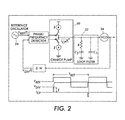
- FIGURE 2 is a phase locked loop component of the generator of Fig. 1 ;
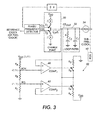
- FIGURE 3 shows a clamping circuit component for association with the sub-pixel clock generator
- FIGURE 4 is a flow chart illustrating a process for optimal switching of charge pump current in a sub-pixel clock generator.
- a sub-pixel clock generator processor 10 is shown wherein eight-bit signals (in a parallel format called the Video Data A 12 and Video Data B 14 for a dual-channel ROS system) are applied to parallel-to-serial converter circuitry 16,18, respectively, to generate the output signals sub-pixel A 20 and sub-pixel B 22.
- the output signals are applied to the laser drivers in the ROS to turn on the laser beam.
- the duration of the laser beam in each on state depends on the width of the output signal pulses.
- the parallel-to-serial converters 16,18 require an internal clock signal eight times faster than the pixel clock 24 to control the maximum duration of the output pulses for the sub-pixel generation.
- the internal clock of the converters requires a sub-pixel clock 26 that is generated by the phase lock loop (PLL) circuit 28.
- PLL phase lock loop
- the PLL part of the SPG chip is optimized for a specific system printing speed by the pixel clock signal 24.
- a system speed of 100 pages per minute (ppm) may require a pixel clock of 54 MHz.
- the sub-pixel clock frequency 26 is eight times faster than the pixel clock (432 MHz which is 8 x 54 MHz).
- the PLL includes a charge pump circuit 30 and a loop filter circuit 32 for communicating a charge pump current, (i cp ) to the VCO 34.
- the charge pump current charges up the capacitors of the loop filter circuit 32 to provide the voltage necessary to set the frequency in the VCO 34.
- a clock frequency should be increased to about 68 MHz so that the new "sub-pixel" clock signal 26 would be 524 MHz (8 x 68 MHz). If the charge pump circuit were to experience a sudden change between the 54 MHz clock and the 68 MHz clock (changing system printing speed from 100 ppm to 135 ppm) such a sudden change in the charge pump current can cause overshoots in the input voltage of the VCO, causing VCO saturation, longer settling time and more jitter.
- the charge pump circuitry 30 provides the current for the loop filter circuit 32 which in turn provides the controlling voltage for the VCO to set the frequency for a VCO clock, which is used as the sub-pixel clock signal 26.
- the VCO For higher speeds, more current from the charge pump circuit must be available for charging up the capacitor in the loop filter 32.
- any increase in this current needs to be effected cautiously because too much current and, more importantly, too sudden a change in the value of the current from the charge pump circuitry, can cause jitter and instability and deteriorate the settling time of the PLL. For example, if the VCO is working between 0 and 5 volts, for a 100 ppm system printing speed, the input voltage to the VCO should be 1.5 volts.
- the off-chip optimizing circuitry 40 interposed between the charge pump 30 and loop filter 32 comprises a comparator circuit wherein when the charge pump current (CPout) is in normal operation, i.e., between 1.1 volts corresponding to a first system printing speed and 2.2 volts corresponding to a second system printing speed, both switches S 3 and S 4 are off.
- the charge pump current CPout
- the charge pump requires 10 microamps to generate the 1.1 volts at the VCO for an output frequency corresponding to the first system printing speed circuitry 40, it has no effect.
- the abrupt change in voltage can cause a voltage spike resulting in the problems identified above.
- the voltage of the VCO may bounce to amounts greater than 2.2 volts or less than 1.1 volts.
- the clamping circuit 40 precludes the bounce in a range exceeding the 1.1 volt to 2.2 volt desired range. If the charge pump current is such as to cause a spike tending to more than 2.2 volts, as determined by comparator 60 then switch S 3 is turned on so that capacitor C 1 within the loop circuit can discharge until the charge pump output voltage is less than or equal 2.2 volts. Then switch S 3 would turn off.
- the charge pump output circuit is less than 1.1 volts as determined by comparator 62, then switch S 4 is turned on and capacitor C 1 is charged up through resistor R 4 until the charge pump output voltage is greater than or equal to 1.1 volts and then switch S 4 is turned off.
- the charge pump output voltage at the VCO is clamped between a limited range.
- the values identified are merely exemplary and circuit components and operational performance can be adjusted as needed for a particular printing system.
- An advantage of the subject clamping and optimizing circuitry of FIGURE 3 is that the SPG chip, initially tuned to a first pixel clock frequency, can have its output safely adjusted through the off-chip clamping circuitry to another pixel clock speed for the desired adjustment of the ROS light source 60 .
- other embodiments could comprise the subject clamping technique in a fully integrated on-chip assembly. In general, this technique can be used on-chip or off-chip.
Landscapes
- Engineering & Computer Science (AREA)
- Multimedia (AREA)
- Signal Processing (AREA)
- Stabilization Of Oscillater, Synchronisation, Frequency Synthesizers (AREA)
- Facsimile Heads (AREA)
- Laser Beam Printer (AREA)
- Exposure Or Original Feeding In Electrophotography (AREA)
- Printers Or Recording Devices Using Electromagnetic And Radiation Means (AREA)
- Facsimile Scanning Arrangements (AREA)
- Ink Jet (AREA)
Abstract
Description
- The present invention relates generally to electrophotographic printing machines, and more particularly, to raster output scanners in electrophotographic printing machines.
- Generally, the process of electrophotographic printing includes charging a photoconductive member to a substantially uniform potential to sensitize its surface. The charged portion of the photoconductive surface is exposed to a light image from a scanning laser beam or a LED diode that corresponds to an original document or image being reproduced. The effect of the light on the charged surface produces an electrostatic latent image on the photoconductive surface.
- After the electrostatic latent image is recorded on the photoconductive surface, the latent image is developed. Two-component and single-component developer materials are commonly used for development. A typical two-component developer comprises a mixture of magnetic carrier granules and toner particles that adhere triboelectrically to the latent image. A single-component developer material is typically comprised of toner particles without carrier particles. Toner particles are attracted to the latent image, forming a toner powder image on the latent image of the photoconductive surface. The toner powder image is subsequently transferred to a copy sheet. Finally, the toner powder image is heated to permanently fuse it to the copy sheet to form the hard copy image.
- In color electrophotographic printers, one or more Raster Output-Scanner (ROS) units are positioned adjacent to a moving photoreceptor belt surface or the like and are selectively energized to generate successive image exposures. Each of the latent images is representative of one of a plurality of different color separation images. Development of the color separation latent images and the transfer of the developed image to an output media define a multi-color image. The color separation images may define, for example, yellow, magenta, cyan, and black color images that, upon subtractive combination on the output media, produce a visible representation of the multi-color image. When an observer looks at the output media, the human eye integrates the light reflections from the color component images into shades of color.
- For a color imaging cycle, the printer generates a component image exposure for each color component of the desired output image. For full color images, four component images may be generated, one component image for each of the three basic colors and a fourth for black images. Each component image is transferred to the moving photoconductive surface by modulating the light source of an ROS as it moves across the moving photoconductor to selectively discharge the photoconductor in an image-wise pattern. The modulation control of the laser or LED of the ROS is provided by the video data. For each color component image, the value of an image data byte is used to enable or disable the laser or LED that illuminates the photoreceptor for one pixel timing period. If the data value is less than a threshold value, the LED or laser is not operated for one pixel period. If the data value indicates that a pixel is to be generated, then the LED or laser is operated for one pixel period.
- An ROS that generates a series of pixels comprising a color component image places the color component image it generates in overlying registration with the other color component images. These overlapping images are composed of a series of closely spaced pixels that are nominally spaced 5 microns apart. When these component images are developed at development stations to transfer toner particles of different colors to the component images, a composite color image is formed. This composite color image is then transferred to an output sheet. Thus, the quality of color image perceived by the observer relies upon the precise registration of the component image pixels.
- In some electrophotographic imaging systems, the latent images of the component image are formed and developed on top of one another in a common imaging region of the photoconductor. The latent images generated in the common imaging region may be formed and developed during multiple passes of the photoconductor around a continuous transport path. Alternatively, the latent images can be formed and developed in a single pass of the photoconductor around the continuous transport path. A single-pass system enables multi-color images to be assembled at extremely high speeds. In either type of imaging systems, accurate placement of the color separation image pixels in the latent image is important for image quality.
- One problem with the pixels generated by these types of ROS devices is the lack of precision regarding the size and placement of the pixels. Because the entire data byte is mapped to only one value, either an on or off value, only one of two types of pixels may be produced. Therefore, the data bytes for an image may define pixels of different densities, but the ROS is only able to generate a pixel that is either on for the full duration of a pixel clock cycle or off for the same period of time. Consequently, some of the data content for an image is lost in the process of generating a latent image from a set of image data.
- Published Application
No. 2006/0215188 A1, September 28, 2006 - As alternative printing system speeds may be desired, there is a need for advantageously utilizing the foregoing existing SPG custom chip, but for different speeds, and to avoid having to develop a new full custom specialized integrated chip respectively for each desired speed.
- Accordingly, it is desired to utilize an existing SPG chip for different or higher speeds by changing only a few off-chip components that may be associated with the chip so that a system can be utilized which quickly and inexpensively switches between the different printing speeds.
- According to aspects illustrated herein there is provided a switchable ROS driver circuit for an electrophotographic system for selectively switching between a plurality of system printing speeds. A sub-pixel clock generator is tuned to a first reference signal corresponding to a first system printing speed for setting an input voltage at a voltage controlled oscillator ("VCO") to generate a desired frequency for the ROS light source corresponding to the first system printing speed. A clamping circuit is associated with the sub-pixel clock generator for settling jitter and avoiding saturation of the input voltage to the VCO upon applying a second reference signal corresponding to a second system printing speed to the sub-pixel generator. The ROS light source is in operative communication with the sub-pixel clock generator for sub-pixel control of the ROS light source.
- Another disclosed feature of the embodiments comprises a method for switching an ROS driver circuit from an electrophotographic system for selective switching of system printing speeds. The first reference signal is applied that corresponds to a first system printing speed, to a pixel clock generator disposed to set an input voltage at a VCO in communication with an ROS light source for generating a first desired frequency corresponding to the first system printing speed. The first reference signal is switched to a second reference signal corresponding to a second reference signal corresponding to a second system printing speed. The input voltage to the VCO is clamped during the switching for settling jitter and avoiding saturation of the input voltage to the VCO. The VCO output corresponding to the second system printing speed frequency is communicated to the ROS light source.
In a further embodiment of the method ofclaim 10 the clamping includes setting a current for a charge pump circuit portion of the pixel clock generator and limiting the input voltage to the VCO within a desired range.
In a further embodiment the clamping includes detecting the input voltage to the VCO at an input loop filter circuit, and charging and discharging the loop filter when the input voltage is lower and higher, respectively, than the desired range.
In one embodiment of the printing system of claim 120 the clamping circuit comprises a comparator for detecting the input voltage to the VCO outside of a preferred range.
In a further embodiment the clamping circuit discharges a loop filter for reducing the input voltage to the VCO when the input voltage is higher than the preferred range, and charges the loop filter for increasing the input voltage to the VCO when the input voltage is lower than the preferred range. -
FIGURE 1 is a block diagram of a sub-pixel clock generator; -
FIGURE 2 is a phase locked loop component of the generator ofFig. 1 ; -
FIGURE 3 shows a clamping circuit component for association with the sub-pixel clock generator; and -
FIGURE 4 is a flow chart illustrating a process for optimal switching of charge pump current in a sub-pixel clock generator. - With reference to
FIGURE 1 , a sub-pixelclock generator processor 10 is shown wherein eight-bit signals (in a parallel format called theVideo Data A 12 andVideo Data B 14 for a dual-channel ROS system) are applied to parallel-to-serial converter circuitry signals sub-pixel A 20 andsub-pixel B 22. The output signals are applied to the laser drivers in the ROS to turn on the laser beam. The duration of the laser beam in each on state depends on the width of the output signal pulses. The parallel-to-serial converters pixel clock 24 to control the maximum duration of the output pulses for the sub-pixel generation. The internal clock of the converters requires asub-pixel clock 26 that is generated by the phase lock loop (PLL)circuit 28. - With reference to
FIGURE 2 , the PLL part of the SPG chip is optimized for a specific system printing speed by thepixel clock signal 24. For example, a system speed of 100 pages per minute (ppm) may require a pixel clock of 54 MHz. Thesub-pixel clock frequency 26 is eight times faster than the pixel clock (432 MHz which is 8 x 54 MHz). The PLL includes acharge pump circuit 30 and aloop filter circuit 32 for communicating a charge pump current, (icp) to theVCO 34. The charge pump current charges up the capacitors of theloop filter circuit 32 to provide the voltage necessary to set the frequency in theVCO 34. - As noted above, when a change is desired in a system's printing speed, for example from 100 ppm to 135 ppm, there needs to be a change in the charge pump current to adjust the voltage to the VCO to adjust laser pulse durations. For the 135 ppm speed, a clock frequency should be increased to about 68 MHz so that the new "sub-pixel"
clock signal 26 would be 524 MHz (8 x 68 MHz). If the charge pump circuit were to experience a sudden change between the 54 MHz clock and the 68 MHz clock (changing system printing speed from 100 ppm to 135 ppm) such a sudden change in the charge pump current can cause overshoots in the input voltage of the VCO, causing VCO saturation, longer settling time and more jitter. - More particularly, as shown in
FIGURE 2 , thecharge pump circuitry 30 provides the current for theloop filter circuit 32 which in turn provides the controlling voltage for the VCO to set the frequency for a VCO clock, which is used as thesub-pixel clock signal 26. For higher speeds, more current from the charge pump circuit must be available for charging up the capacitor in theloop filter 32. However, any increase in this current needs to be effected cautiously because too much current and, more importantly, too sudden a change in the value of the current from the charge pump circuitry, can cause jitter and instability and deteriorate the settling time of the PLL. For example, if the VCO is working between 0 and 5 volts, for a 100 ppm system printing speed, the input voltage to the VCO should be 1.5 volts. To get the desired output frequency for the 135 ppm system printing speed there would be an increase in the voltage value in the adjustment to approximately 2 volts. In transition between the different voltage levels to the VCO it is not uncommon to generate voltage spikes up to the system voltage limit, 5 volts, before there is a settling down to the desirable voltage of 2 volts. Such saturating spikes to the VCO disable the clock frequency to the point that there can be no printing until the proper frequency has been realized after a certain settling time. The jumping up and down of the voltage is called "jitter" and the time that it takes for the jitter to end is called a "settling time". - In order to optimize the PLL operation in situations where frequent switching between different printing speeds occurs, and hence clock frequency changes are required, it is best to make the changes in input voltage to the VCO clamped in a range that would avoid undesirable jitter and oscillator saturation within a reasonable settling time.
- With reference to
FIGURES 3 and4 , it can be seen that the off-chip optimizing circuitry 40 interposed between thecharge pump 30 andloop filter 32 comprises a comparator circuit wherein when the charge pump current (CPout) is in normal operation, i.e., between 1.1 volts corresponding to a first system printing speed and 2.2 volts corresponding to a second system printing speed, both switches S3 and S4 are off. Thus, for example, if the charge pump requires 10 microamps to generate the 1.1 volts at the VCO for an output frequency corresponding to the first systemprinting speed circuitry 40, it has no effect. Alternatively, when the charge pump circuit is adjusted to increase an output of approximately 12 microamps to charge the loop filter circuit to approximately 2.2 volts as the input to the VCO for outputting a second frequency corresponding to a second printing system speed, then the abrupt change in voltage can cause a voltage spike resulting in the problems identified above. - More particularly, if the pixel clock is set to the first frequency according to the first
system printing speed 50 and then it is abruptly increased 52 to a current to adjust the VCO for a pixel clock output to a second frequency corresponding to a second system printing speed, then the voltage of the VCO may bounce to amounts greater than 2.2 volts or less than 1.1 volts. The clampingcircuit 40 precludes the bounce in a range exceeding the 1.1 volt to 2.2 volt desired range. If the charge pump current is such as to cause a spike tending to more than 2.2 volts, as determined bycomparator 60 then switch S3 is turned on so that capacitor C1 within the loop circuit can discharge until the charge pump output voltage is less than or equal 2.2 volts. Then switch S3 would turn off. Alternatively, if the charge pump output circuit is less than 1.1 volts as determined bycomparator 62, then switch S4 is turned on and capacitor C1 is charged up through resistor R4 until the charge pump output voltage is greater than or equal to 1.1 volts and then switch S4 is turned off. Thus, the charge pump output voltage at the VCO is clamped between a limited range. The values identified are merely exemplary and circuit components and operational performance can be adjusted as needed for a particular printing system. - An advantage of the subject clamping and optimizing circuitry of
FIGURE 3 is that the SPG chip, initially tuned to a first pixel clock frequency, can have its output safely adjusted through the off-chip clamping circuitry to another pixel clock speed for the desired adjustment of the ROSlight source 60. However, other embodiments could comprise the subject clamping technique in a fully integrated on-chip assembly. In general, this technique can be used on-chip or off-chip.
Claims (10)
- A switchable ROS driver circuit for an electrophotographic system for selective switching between a plurality of system printing speeds comprising:a sub-pixel clock generator tuned to a first reference signal corresponding to a first printing system speed and including a phase locked loop circuit, a charge pump circuit and a loop filter disposed to set an input voltage at a VCO to generate a desired frequency corresponding to the first system printing speed;a clamping circuit associated with the sub-pixel clock generator for settling jitter and avoiding saturation of the input voltage to the VCO upon applying a second reference signal corresponding to a second system printing speed to the sub-pixel clock generator; andan ROS light source in operative communication with the sub-pixel clock generator for sub-pixel control of the ROS light source.
- The driver circuit of claim 1 wherein the sub-pixel clock generator comprises a custom mixed-mode integrated chip, and the clamping circuit comprises off-chip component circuitry.
- The driver circuit of claim 2 wherein the clamping circuit includes a first circuit portion for setting current for the charge pump circuit and a second circuit portion for clamping the input voltage to the VCO within a desired range.
- The driver circuit of claim 2 wherein the second circuit portion comprises a resistive and analog switch assembly for inhibiting the jitter and the saturation.
- The driver circuit of claim 2 wherein the clamping circuit is effectively disposed between the loop filter circuit and an input to the VCO.
- The driver circuit of claim 1 wherein the clamping circuit comprises a comparator for detecting the input voltage to the VCO outside of a preferred range.
- The driver circuit of claim 6 wherein the clamping circuit discharges a loop filter for reducing the input voltage to the VCO when the input voltage is higher than the preferred range, and charges the loop filter for increasing the input voltage to the VCO when the input voltage is lower than the preferred range.
- A method for switching an ROS driver circuit for an electrophotographic system for selective switching of system printing speeds, comprising:applying a first reference signal corresponding to a first system printing speed to a pixel clock generator disposed to set an input voltage at a VCO in communication with an ROS light source for generating a first desired frequency corresponding to the first system printing speed;switching the first reference signal to a second reference signal corresponding to a second system printing speed;clamping the input voltage to the VCO during the switching for settling jitter and avoiding saturation of the input voltage to the VCO; andcommunicating the VCO output frequency corresponding to the second system printing speed to the ROS light source.
- The method of claim 8 wherein the generating the first desired frequency is executed with an integrated chip and the clamping is executed with off-chip component circuitry.
- A xerographic printing system for selective switching between a plurality of system printing speeds comprising:a sub-pixel clock generator tuned to a first reference signal corresponding to a first printing system speed and including a phase locked loop circuit, a charge pump circuit and a loop filter disposed to set an input voltage at a VCO to generate a desired frequency corresponding to the first system printing speed; anda clamping circuit associated with the sub-pixel clock generator for settling jitter and avoiding saturation of the input voltage to the VCO upon applying a second reference signal corresponding to a second system printing speed to the sub-pixel clock generator.
Applications Claiming Priority (1)
| Application Number | Priority Date | Filing Date | Title |
|---|---|---|---|
| US11/657,204 US8693048B2 (en) | 2007-01-24 | 2007-01-24 | Sub-pixel generation for high speed color laser printers using a clamping technique for PLL (phase locked loop) circuitry |
Publications (3)
| Publication Number | Publication Date |
|---|---|
| EP1950949A2 true EP1950949A2 (en) | 2008-07-30 |
| EP1950949A3 EP1950949A3 (en) | 2009-04-15 |
| EP1950949B1 EP1950949B1 (en) | 2014-07-30 |
Family
ID=39319648
Family Applications (1)
| Application Number | Title | Priority Date | Filing Date |
|---|---|---|---|
| EP08150483.9A Ceased EP1950949B1 (en) | 2007-01-24 | 2008-01-22 | Sub-pixel generation for high speed color laser printers using a clamping technique for PLL (phase locked loop) circuitry |
Country Status (6)
| Country | Link |
|---|---|
| US (1) | US8693048B2 (en) |
| EP (1) | EP1950949B1 (en) |
| JP (1) | JP5308681B2 (en) |
| BR (1) | BRPI0800181A (en) |
| CA (1) | CA2618401C (en) |
| MX (1) | MX2008000809A (en) |
Families Citing this family (3)
| Publication number | Priority date | Publication date | Assignee | Title |
|---|---|---|---|---|
| JP2017219586A (en) * | 2016-06-03 | 2017-12-14 | 株式会社ジャパンディスプレイ | Signal supply circuit and display device |
| WO2019212525A1 (en) | 2018-04-30 | 2019-11-07 | Hewlett-Packard Development Company, L.P. | Isolating electrical components |
| CN111123671A (en) * | 2018-11-01 | 2020-05-08 | 联想图像(天津)科技有限公司 | Frequency conversion circuit, exposure device and printer |
Citations (1)
| Publication number | Priority date | Publication date | Assignee | Title |
|---|---|---|---|---|
| US20060215188A1 (en) | 2005-03-25 | 2006-09-28 | Xerox Corporation | Method and system for improved raster output scan control in an electrophotographic system |
Family Cites Families (33)
| Publication number | Priority date | Publication date | Assignee | Title |
|---|---|---|---|---|
| JPH0642020B2 (en) * | 1985-07-31 | 1994-06-01 | 株式会社リコー | Optical scanning device |
| US5140349A (en) * | 1988-09-27 | 1992-08-18 | Canon Kabushiki Kaisha | Recording apparatus |
| EP0416832B1 (en) * | 1989-09-07 | 1996-07-10 | Canon Kabushiki Kaisha | Image forming apparatus |
| US5502419A (en) * | 1992-06-05 | 1996-03-26 | Canon Kabushiki Kaisha | Pulse width modulation signal generation and triangular wave signal generator for the same |
| US5329252A (en) * | 1992-11-05 | 1994-07-12 | Northern Telecom Limited | Slew-rate limited voltage controlled oscillator control voltage clamp circuit |
| US5471314A (en) * | 1993-06-14 | 1995-11-28 | Eastman Kodak Company | Line start synchronizer for raster scanner |
| US5361123A (en) * | 1993-08-23 | 1994-11-01 | Xerox Corporation | Microcontroller based xerographic charge device power supply |
| US5493374A (en) * | 1994-03-07 | 1996-02-20 | Xerox Corporation | Apparatus for controlling sheet velocity |
| US5517230A (en) * | 1994-09-19 | 1996-05-14 | Xerox Corporation | Control system for a variable-resolution raster output scanner |
| US5530642A (en) * | 1994-11-14 | 1996-06-25 | Xerox Corporation | Control system for aspect ratio and magnification of a raster output scanner |
| US6133932A (en) * | 1994-12-19 | 2000-10-17 | Xerox Corporation | Method and apparatus for adjusting a line synchronization signal in response to photoreceptor motion |
| JPH0964727A (en) * | 1995-08-23 | 1997-03-07 | Toshiba Corp | Synchronous circuit |
| JP4066500B2 (en) * | 1998-04-08 | 2008-03-26 | ソニー株式会社 | PLL circuit |
| US6674824B1 (en) * | 1998-08-18 | 2004-01-06 | National Science Council | Method and circuitry for controlling a phase-locked loop by analog and digital signals |
| US6184916B1 (en) * | 1999-01-19 | 2001-02-06 | Xerox Corporation | Multiple-pulse, pulse width and position modulation systems and methods |
| JP2000355122A (en) * | 1999-06-16 | 2000-12-26 | Canon Inc | Image forming device |
| US6151152A (en) * | 1999-12-21 | 2000-11-21 | Xerox Corporation | Reference frequency and facet to facet error correction circuit |
| US6288574B1 (en) * | 1999-12-21 | 2001-09-11 | Xerox Corporation | Digital phase detector |
| US6794946B2 (en) * | 2000-05-22 | 2004-09-21 | Ramin Farjad-Rad | Frequency acquisition for data recovery loops |
| US7050080B2 (en) * | 2000-06-05 | 2006-05-23 | Ricoh Company, Ltd. | Image forming apparatus for controlling image writing by adjusting image clock |
| US6657488B1 (en) * | 2001-07-03 | 2003-12-02 | Silicon Laboratories, Inc. | Offset correction and slicing level adjustment for amplifier circuits |
| US6947515B2 (en) * | 2001-12-21 | 2005-09-20 | Xerox Corporation | Method for measuring the response of a voltage controlled oscillator |
| US6529055B1 (en) * | 2001-12-21 | 2003-03-04 | Xerox Corporation | Method for adjusting the center frequency of a phase locked loop |
| US6940536B2 (en) * | 2002-11-07 | 2005-09-06 | Xerox Corporation | System architecture for scan line non-linearity compensation in a ROS system |
| JP2004163792A (en) * | 2002-11-15 | 2004-06-10 | Fuji Photo Film Co Ltd | Radiation image reader |
| US6903585B2 (en) * | 2003-06-27 | 2005-06-07 | Analog Devices, Inc. | Pulse width modulated common mode feedback loop and method for differential charge pump |
| US7053684B1 (en) * | 2004-04-28 | 2006-05-30 | Cirrus Logic, Inc. | Reduced jitter charge pumps and circuits and systems utilizing the same |
| JP2006021480A (en) * | 2004-07-09 | 2006-01-26 | Ricoh Printing Systems Ltd | Image forming apparatus |
| JP2006159222A (en) * | 2004-12-03 | 2006-06-22 | Mitsubishi Materials Corp | Microporosity generation prediction method, microporosity generation prediction program, and recording medium |
| JP4645205B2 (en) * | 2005-01-20 | 2011-03-09 | 富士ゼロックス株式会社 | Optical scanning apparatus and image forming apparatus |
| US7852510B2 (en) * | 2005-04-28 | 2010-12-14 | Xerox Corporation | Systems and methods for setting configuring rendering parameters for high-speed rendering devices |
| US7429895B2 (en) * | 2006-02-28 | 2008-09-30 | Texas Instruments Incorporated | Systems and methods for drift compensation in a control circuit |
| US8488186B2 (en) * | 2007-01-24 | 2013-07-16 | Xerox Corporation | Gradual charge pump technique for optimizing phase locked loop (PLL) function in sub-pixel generation for high speed laser printers switching between different speeds |
-
2007
- 2007-01-24 US US11/657,204 patent/US8693048B2/en not_active Expired - Fee Related
-
2008
- 2008-01-16 CA CA2618401A patent/CA2618401C/en not_active Expired - Fee Related
- 2008-01-17 MX MX2008000809A patent/MX2008000809A/en active IP Right Grant
- 2008-01-17 BR BRPI0800181-2A patent/BRPI0800181A/en not_active IP Right Cessation
- 2008-01-22 EP EP08150483.9A patent/EP1950949B1/en not_active Ceased
- 2008-01-24 JP JP2008013353A patent/JP5308681B2/en not_active Expired - Fee Related
Patent Citations (1)
| Publication number | Priority date | Publication date | Assignee | Title |
|---|---|---|---|---|
| US20060215188A1 (en) | 2005-03-25 | 2006-09-28 | Xerox Corporation | Method and system for improved raster output scan control in an electrophotographic system |
Also Published As
| Publication number | Publication date |
|---|---|
| MX2008000809A (en) | 2009-02-23 |
| EP1950949A3 (en) | 2009-04-15 |
| CA2618401C (en) | 2012-05-22 |
| US20080174348A1 (en) | 2008-07-24 |
| BRPI0800181A (en) | 2008-09-16 |
| CA2618401A1 (en) | 2008-07-24 |
| US8693048B2 (en) | 2014-04-08 |
| JP5308681B2 (en) | 2013-10-09 |
| JP2008179145A (en) | 2008-08-07 |
| EP1950949B1 (en) | 2014-07-30 |
Similar Documents
| Publication | Publication Date | Title |
|---|---|---|
| DE69519504T2 (en) | Image processing method and device | |
| US7940422B2 (en) | Image forming apparatus | |
| US5469266A (en) | Color image processing apparatus which uses different screen angles for different color components | |
| US8488186B2 (en) | Gradual charge pump technique for optimizing phase locked loop (PLL) function in sub-pixel generation for high speed laser printers switching between different speeds | |
| US4681424A (en) | Compensation for fine line prints | |
| US5404156A (en) | Method and apparatus for forming a full-color image | |
| CA2618401C (en) | Sub-pixel generation for high speed color laser printers using a clamping technique for pll (phase locked loop) circuitry | |
| JPH11317871A (en) | Pulse width modulation circuit | |
| US6219085B1 (en) | Method and system for improved performance of adjustable printer clocks in an electrophotographic device | |
| US6163334A (en) | Image forming device | |
| JP4289771B2 (en) | Frequency synthesizer and frequency conversion method | |
| JPH063932A (en) | High voltage power source device | |
| EP1220526A2 (en) | Clock generating circuit and image-forming apparatus | |
| US7649544B2 (en) | Method and system for improved raster output scan control in an electrophotographic system | |
| US6111593A (en) | Using multiple digitally-produced exposure levels to compensate for laser absorption in read image-on-image xerography | |
| US7042484B2 (en) | Scan line length adjustment | |
| US7315320B2 (en) | Optical writing system and method, and image forming apparatus receiving an external parameter | |
| US7116746B2 (en) | Synchronous clock phase control circuit | |
| US6181357B1 (en) | Method and system for the modification of the timing of a plurality of PEL clocks in an electrophotographic device | |
| JPH11254750A5 (en) | ||
| KR960007512B1 (en) | High Voltage Power Control | |
| JP3130916B2 (en) | Multicolor image forming device | |
| JP3012311B2 (en) | Color image forming equipment | |
| JPH06284276A (en) | Image forming device | |
| JP2017026725A (en) | Image forming apparatus and image forming method |
Legal Events
| Date | Code | Title | Description |
|---|---|---|---|
| PUAI | Public reference made under article 153(3) epc to a published international application that has entered the european phase |
Free format text: ORIGINAL CODE: 0009012 |
|
| AK | Designated contracting states |
Kind code of ref document: A2 Designated state(s): AT BE BG CH CY CZ DE DK EE ES FI FR GB GR HR HU IE IS IT LI LT LU LV MC MT NL NO PL PT RO SE SI SK TR |
|
| AX | Request for extension of the european patent |
Extension state: AL BA MK RS |
|
| PUAL | Search report despatched |
Free format text: ORIGINAL CODE: 0009013 |
|
| AK | Designated contracting states |
Kind code of ref document: A3 Designated state(s): AT BE BG CH CY CZ DE DK EE ES FI FR GB GR HR HU IE IS IT LI LT LU LV MC MT NL NO PL PT RO SE SI SK TR |
|
| AX | Request for extension of the european patent |
Extension state: AL BA MK RS |
|
| RIC1 | Information provided on ipc code assigned before grant |
Ipc: H04N 1/405 20060101ALI20090309BHEP Ipc: H04N 1/053 20060101AFI20090309BHEP |
|
| 17P | Request for examination filed |
Effective date: 20091015 |
|
| AKX | Designation fees paid |
Designated state(s): DE FR GB |
|
| 17Q | First examination report despatched |
Effective date: 20091201 |
|
| GRAP | Despatch of communication of intention to grant a patent |
Free format text: ORIGINAL CODE: EPIDOSNIGR1 |
|
| INTG | Intention to grant announced |
Effective date: 20131118 |
|
| GRAP | Despatch of communication of intention to grant a patent |
Free format text: ORIGINAL CODE: EPIDOSNIGR1 |
|
| INTG | Intention to grant announced |
Effective date: 20140220 |
|
| GRAS | Grant fee paid |
Free format text: ORIGINAL CODE: EPIDOSNIGR3 |
|
| GRAA | (expected) grant |
Free format text: ORIGINAL CODE: 0009210 |
|
| AK | Designated contracting states |
Kind code of ref document: B1 Designated state(s): DE FR GB |
|
| REG | Reference to a national code |
Ref country code: GB Ref legal event code: FG4D |
|
| REG | Reference to a national code |
Ref country code: DE Ref legal event code: R096 Ref document number: 602008033538 Country of ref document: DE Effective date: 20140911 |
|
| REG | Reference to a national code |
Ref country code: DE Ref legal event code: R097 Ref document number: 602008033538 Country of ref document: DE |
|
| PLBE | No opposition filed within time limit |
Free format text: ORIGINAL CODE: 0009261 |
|
| STAA | Information on the status of an ep patent application or granted ep patent |
Free format text: STATUS: NO OPPOSITION FILED WITHIN TIME LIMIT |
|
| 26N | No opposition filed |
Effective date: 20150504 |
|
| REG | Reference to a national code |
Ref country code: FR Ref legal event code: PLFP Year of fee payment: 9 |
|
| REG | Reference to a national code |
Ref country code: FR Ref legal event code: PLFP Year of fee payment: 10 |
|
| REG | Reference to a national code |
Ref country code: FR Ref legal event code: PLFP Year of fee payment: 11 |
|
| PGFP | Annual fee paid to national office [announced via postgrant information from national office to epo] |
Ref country code: FR Payment date: 20171221 Year of fee payment: 11 |
|
| PGFP | Annual fee paid to national office [announced via postgrant information from national office to epo] |
Ref country code: GB Payment date: 20171222 Year of fee payment: 11 |
|
| PGFP | Annual fee paid to national office [announced via postgrant information from national office to epo] |
Ref country code: DE Payment date: 20171218 Year of fee payment: 11 |
|
| REG | Reference to a national code |
Ref country code: DE Ref legal event code: R119 Ref document number: 602008033538 Country of ref document: DE |
|
| GBPC | Gb: european patent ceased through non-payment of renewal fee |
Effective date: 20190122 |
|
| PG25 | Lapsed in a contracting state [announced via postgrant information from national office to epo] |
Ref country code: FR Free format text: LAPSE BECAUSE OF NON-PAYMENT OF DUE FEES Effective date: 20190131 Ref country code: DE Free format text: LAPSE BECAUSE OF NON-PAYMENT OF DUE FEES Effective date: 20190801 |
|
| PG25 | Lapsed in a contracting state [announced via postgrant information from national office to epo] |
Ref country code: GB Free format text: LAPSE BECAUSE OF NON-PAYMENT OF DUE FEES Effective date: 20190122 |