EP1950945A1 - Optical element for a document illuminator - Google Patents
Optical element for a document illuminator Download PDFInfo
- Publication number
- EP1950945A1 EP1950945A1 EP08100592A EP08100592A EP1950945A1 EP 1950945 A1 EP1950945 A1 EP 1950945A1 EP 08100592 A EP08100592 A EP 08100592A EP 08100592 A EP08100592 A EP 08100592A EP 1950945 A1 EP1950945 A1 EP 1950945A1
- Authority
- EP
- European Patent Office
- Prior art keywords
- optical element
- light
- prisms
- defining
- light sources
- Prior art date
- Legal status (The legal status is an assumption and is not a legal conclusion. Google has not performed a legal analysis and makes no representation as to the accuracy of the status listed.)
- Granted
Links
- 230000003287 optical effect Effects 0.000 title claims abstract description 26
- URYAFVKLYSEINW-UHFFFAOYSA-N Chlorfenethol Chemical compound C=1C=C(Cl)C=CC=1C(O)(C)C1=CC=C(Cl)C=C1 URYAFVKLYSEINW-UHFFFAOYSA-N 0.000 claims 1
- 239000003989 dielectric material Substances 0.000 abstract description 2
- 238000005286 illumination Methods 0.000 description 5
- 238000003384 imaging method Methods 0.000 description 5
- 238000003491 array Methods 0.000 description 2
- 230000005540 biological transmission Effects 0.000 description 2
- 238000002955 isolation Methods 0.000 description 2
- 239000011248 coating agent Substances 0.000 description 1
- 238000000576 coating method Methods 0.000 description 1
- 230000000295 complement effect Effects 0.000 description 1
- 238000005520 cutting process Methods 0.000 description 1
- 230000007547 defect Effects 0.000 description 1
- 238000009826 distribution Methods 0.000 description 1
- 230000000694 effects Effects 0.000 description 1
- 239000011521 glass Substances 0.000 description 1
- 238000004519 manufacturing process Methods 0.000 description 1
- 239000000463 material Substances 0.000 description 1
- 229910044991 metal oxide Inorganic materials 0.000 description 1
- 150000004706 metal oxides Chemical class 0.000 description 1
- 238000000034 method Methods 0.000 description 1
- 238000000465 moulding Methods 0.000 description 1
- 230000000737 periodic effect Effects 0.000 description 1
- 238000002310 reflectometry Methods 0.000 description 1
- 239000004065 semiconductor Substances 0.000 description 1
- 239000000758 substrate Substances 0.000 description 1
Images

Classifications
-
- G—PHYSICS
- G02—OPTICS
- G02B—OPTICAL ELEMENTS, SYSTEMS OR APPARATUS
- G02B5/00—Optical elements other than lenses
- G02B5/04—Prisms
-
- G—PHYSICS
- G02—OPTICS
- G02B—OPTICAL ELEMENTS, SYSTEMS OR APPARATUS
- G02B19/00—Condensers, e.g. light collectors or similar non-imaging optics
- G02B19/0033—Condensers, e.g. light collectors or similar non-imaging optics characterised by the use
- G02B19/0047—Condensers, e.g. light collectors or similar non-imaging optics characterised by the use for use with a light source
- G02B19/0061—Condensers, e.g. light collectors or similar non-imaging optics characterised by the use for use with a light source the light source comprising a LED
- G02B19/0066—Condensers, e.g. light collectors or similar non-imaging optics characterised by the use for use with a light source the light source comprising a LED in the form of an LED array
-
- G—PHYSICS
- G02—OPTICS
- G02B—OPTICAL ELEMENTS, SYSTEMS OR APPARATUS
- G02B19/00—Condensers, e.g. light collectors or similar non-imaging optics
- G02B19/0004—Condensers, e.g. light collectors or similar non-imaging optics characterised by the optical means employed
- G02B19/0028—Condensers, e.g. light collectors or similar non-imaging optics characterised by the optical means employed refractive and reflective surfaces, e.g. non-imaging catadioptric systems
-
- G—PHYSICS
- G02—OPTICS
- G02B—OPTICAL ELEMENTS, SYSTEMS OR APPARATUS
- G02B6/00—Light guides; Structural details of arrangements comprising light guides and other optical elements, e.g. couplings
-
- H—ELECTRICITY
- H04—ELECTRIC COMMUNICATION TECHNIQUE
- H04N—PICTORIAL COMMUNICATION, e.g. TELEVISION
- H04N1/00—Scanning, transmission or reproduction of documents or the like, e.g. facsimile transmission; Details thereof
- H04N1/024—Details of scanning heads ; Means for illuminating the original
- H04N1/028—Details of scanning heads ; Means for illuminating the original for picture information pick-up
- H04N1/02815—Means for illuminating the original, not specific to a particular type of pick-up head
-
- H—ELECTRICITY
- H04—ELECTRIC COMMUNICATION TECHNIQUE
- H04N—PICTORIAL COMMUNICATION, e.g. TELEVISION
- H04N1/00—Scanning, transmission or reproduction of documents or the like, e.g. facsimile transmission; Details thereof
- H04N1/024—Details of scanning heads ; Means for illuminating the original
- H04N1/028—Details of scanning heads ; Means for illuminating the original for picture information pick-up
- H04N1/02815—Means for illuminating the original, not specific to a particular type of pick-up head
- H04N1/02845—Means for illuminating the original, not specific to a particular type of pick-up head using an elongated light source, e.g. tubular lamp, LED array
- H04N1/02865—Means for illuminating the original, not specific to a particular type of pick-up head using an elongated light source, e.g. tubular lamp, LED array using an array of light sources or a combination of such arrays, e.g. an LED bar
Definitions
- the present disclosure relates to an illuminating apparatus used to illuminate hard-copy documents for digital recording, such as in digital scanners, facsimile machines, and digital copiers.
- One type of illuminator useful in document scanning includes a light-transmissive element that exploits internal reflections to direct light from one or more point sources, such as light emitting diodes (LEDs) to emerge from an exit surface of the element toward a document.
- LEDs light emitting diodes
- Designing an illuminator for a scanner presents challenges in providing, among other aspects, an even illumination along the narrow strip of the document, as well as providing a suitable illumination profile across the narrow strip.
- the angular distribution of light produced by the illuminator at the document can vary along the illuminated strip, depending upon the illuminator architecture. Irregularities in the illumination level in the illuminated area can result in defects in the image data, particularly in the case of discrete light sources, such as LEDs. While light guides are able to focus light with high efficiency on the imaging area of the platen, it has been found that glossy document surfaces that are uneven, e.g., crumpled or curved from the platen, may specularly reflect the light toward the photosensitive device unevenly, resulting in bright spots in the image.
- specular flare light is created when a combination of conditions (such as a glossy document not lying perpendicular to the optical axis of the imaging lens) enables a portion of the light from the illumination source to specularly reflect into the imaging sensor and add to its signal output.
- the specular flare light is an undesired addition to the light signal picked up from the light diffused by the document.
- This creates an artifact that may or may not be objectionable to customers depending upon the conditions.
- the artifact is usually noticeable on edges along the fast scan direction (potentially both leading and trailing edges).
- the specular flare artifact is usually a continuous line; for discrete sources, such as LED arrays, the specular flare artifact is discontinuous and periodic, often appearing as bright spots in the image.
- an optical element for transmitting light emitted from a linear array of light sources.
- the optical element includes a light-transmissive member, for example having a refractive index of about 1.4 to about 1.8, and defining an entry surface for disposal near the light sources, the entry surface defining at least one set of prisms, an exit surface, and a section of, typically a DCPC, between the entry surface and the exit surface.
- FIG. 1 is a simplified elevational view of a document scanner.
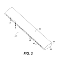
- FIG. 2 is a perspective view of one embodiment of an optical element (light guide), in isolation, for the document scanner of FIG. 1 .
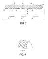
- FIG. 3 is a sectional view, through line 3-3 in FIG. 2 .
- FIG. 4 is a sectional view showing a detail of FIG. 3 .
- the exemplary embodiment also relates to a method of scanning physical documents for generating scanned images.
- the documents to be scanned may comprise sheets of paper or other flexible substrate, on which an image or images to be scanned is disposed.
- the scanner may form a part of an imaging device, such as a stand-alone scanner, a copier, a facsimile machine, or a multifunction device, in which a scanned image is rendered on paper and/or stored in digital form, for example, for display, processing, or transmission in digital form.
- a document scanner includes a platen 10, which may have distinct parts, on which a document sheet 12 can be placed for recording therefrom.
- a document handler (not shown), which sequentially feeds sheets from a multi-page original document.
- the document 12 lies flat on the platen. It is shown curved in Fig.1 to indicate specular reflection conditions that might exist at the edge of a book or if the document is crumpled or otherwise curved.
- a scan head 16 is positioned to illuminate the document and includes an illuminator 18 and a detector 20.
- the detector includes a photosensitive device 22 and a lens arrangement 24.
- Light from a linear array of light sources 50 travels through an optical element 30, which will be described in detail below, and illuminates a thin strip of the document.
- the detector includes a suitable processing device (not shown) for generating an image comprising signals representative of reflected light recorded by the photosensitive device.
- the photosensitive device 22 which includes one or more linear arrays of photosensors, records the reflected light.
- the photosensors may comprise solid-state devices, such as CCD (charge coupled device) or CMOS (complementary metal oxide semiconductor) devices.
- the scan head 16 can be mounted on a moveable carriage 26, for recording light reflected from images on sheets placed on the main portion of platen 10. In general, the carriage translates in direction A, as shown in FIG. 1 .
- FIG. 2 is a perspective view of one embodiment of an optical element 30, in isolation, for the document scanner of FIG. 1 .
- the optical element 30 is formed from a single piece of light-transmissive material, such as glass or plastic, having a refractive index of about 1.4 to about 1.8 (a typical plastic used in this context has a refractive index of about 1.52).
- Element 30 defines an entry surface generally indicated as 34 and an exit surface generally indicated as 38.
- the cross-section such as 36 of the element 30 defines at least a section of a DCPC (dielectric compound parabolic concentrator), as such an optical element is described in, for example, U.S. Patent Application No. 2007-0247677A .
- the DCPC relies on total internal reflection to provide a desirable arrangement of beams emerging from the exit surface 38.
- FIG. 3 is a sectional view, through line 3-3 in FIG. 2 , giving a detailed view of some sets of prisms.
- the prisms can effectively be formed by molding or cutting ridges in the body of element 30, creating the prisms between the ridges.
- Element 30 extends in a direction corresponding to the linear array 50 of light sources, and each prism is oriented, as shown, in a direction perpendicular to the direction along the linear array.
- Each set of prisms 40 is placed to be adjacent a light source 50 providing light into entry surface 34.
- the shortest distance d between the surface of each LED 50 and the set of prisms 40 should be less than 2 mm, and in some instances the LED 50 can contact the prisms.
- the sets 40 of prisms alternate with gap regions 42, which might be painted or otherwise coated with a coating of about 80% reflectivity, with regard to light traveling within element 30.
- FIG. 4 is a detailed view of a single prism 44 defined by adjacent ridges in a set of prisms 40.
- the base p of each prism 44 should be about 0.2 mm to about 1.0 mm in length.
- Each prism 44 defines an angle ⁇ , defined relative to the horizontal line as shown.
- the angle ⁇ is chosen such that, in case of specular reflection, the light exiting the light guide is outside the collection of the angle of the lens or optics used in the scanner. This angle is typically 48 degrees or higher if an SLA-09 lens is used.
- SLA -12 and SLA-20 lenses the ⁇ values are equal to or higher than 52° and 55°, respectively.
- the prism angle will be chosen such that the light coming out of the light guide is outside the acceptance angle of that lens.
- each prism 44 and between each prism 44 should be as small as possible.
- each set 40 of prisms along the element 30 should extend beyond the LED 50 corresponding to the set on both sides, and in the present embodiment could be up to four times the length of the LED 50.
- the embodiment provides an illumination system whereby specular flare effects, such as from a glossy original image, or an image not in direct contact with platen 10, can be minimized while the diffuse component of light is not affected.
- the DCPC as disclosed in U.S. Patent Application No. 2007-0247677A , maximizes the amount of light transferred from the LED sources to the document plane.
- the prisms ensure that the light reaching the document plane has angles greater than the acceptance angle of the imaging lens, thus ensuring that any specularly-reflected light is not imaged by the lens.
- a SELFOC® lens has a very well defined, and not too large, acceptance angle at each point along the lens, so the prism design is relatively uniform. In a practical application, the angle ⁇ on any portion of the prism must be greater than 48°; otherwise light would be transmitted within the acceptance angle of the SELFOC® lens. This means other surface relief structures in the prior art, such as dimples, etc., that have some portion of the surface slope less than the minimum angle for avoiding transmission of light within the acceptance angle of the SELFOC® lens, will not work as efficiently.
Landscapes
- Physics & Mathematics (AREA)
- General Physics & Mathematics (AREA)
- Optics & Photonics (AREA)
- Engineering & Computer Science (AREA)
- Multimedia (AREA)
- Signal Processing (AREA)
- Light Sources And Details Of Projection-Printing Devices (AREA)
- Facsimile Scanning Arrangements (AREA)
- Optical Elements Other Than Lenses (AREA)
Abstract
Description
- The present disclosure relates to an illuminating apparatus used to illuminate hard-copy documents for digital recording, such as in digital scanners, facsimile machines, and digital copiers.
- One type of illuminator useful in document scanning includes a light-transmissive element that exploits internal reflections to direct light from one or more point sources, such as light emitting diodes (LEDs) to emerge from an exit surface of the element toward a document. Designing an illuminator for a scanner presents challenges in providing, among other aspects, an even illumination along the narrow strip of the document, as well as providing a suitable illumination profile across the narrow strip.
- The angular distribution of light produced by the illuminator at the document can vary along the illuminated strip, depending upon the illuminator architecture. Irregularities in the illumination level in the illuminated area can result in defects in the image data, particularly in the case of discrete light sources, such as LEDs. While light guides are able to focus light with high efficiency on the imaging area of the platen, it has been found that glossy document surfaces that are uneven, e.g., crumpled or curved from the platen, may specularly reflect the light toward the photosensitive device unevenly, resulting in bright spots in the image.
- In a practical application of document scanning, specular flare light is created when a combination of conditions (such as a glossy document not lying perpendicular to the optical axis of the imaging lens) enables a portion of the light from the illumination source to specularly reflect into the imaging sensor and add to its signal output. The specular flare light is an undesired addition to the light signal picked up from the light diffused by the document. This creates an artifact that may or may not be objectionable to customers depending upon the conditions. The artifact is usually noticeable on edges along the fast scan direction (potentially both leading and trailing edges). The glossier the document, and the darker the image content, the more the specular flare artifact is enhanced. For uniform sources, such as fluorescent lamps, the specular flare artifact is usually a continuous line; for discrete sources, such as LED arrays, the specular flare artifact is discontinuous and periodic, often appearing as bright spots in the image.
- According to one aspect, there is provided an optical element for transmitting light emitted from a linear array of light sources. The optical element includes a light-transmissive member, for example having a refractive index of about 1.4 to about 1.8, and defining an entry surface for disposal near the light sources, the entry surface defining at least one set of prisms, an exit surface, and a section of, typically a DCPC, between the entry surface and the exit surface.
-
FIG. 1 is a simplified elevational view of a document scanner. -
FIG. 2 is a perspective view of one embodiment of an optical element (light guide), in isolation, for the document scanner ofFIG. 1 . -
FIG. 3 is a sectional view, through line 3-3 inFIG. 2 . -
FIG. 4 is a sectional view showing a detail ofFIG. 3 . - Aspects of the exemplary embodiment relate to an optical element and to a document scanning apparatus or "scanner" which incorporates the optical element. The exemplary embodiment also relates to a method of scanning physical documents for generating scanned images. The documents to be scanned may comprise sheets of paper or other flexible substrate, on which an image or images to be scanned is disposed. The scanner may form a part of an imaging device, such as a stand-alone scanner, a copier, a facsimile machine, or a multifunction device, in which a scanned image is rendered on paper and/or stored in digital form, for example, for display, processing, or transmission in digital form.
- With reference to
FIG. 1 , a document scanner includes aplaten 10, which may have distinct parts, on which adocument sheet 12 can be placed for recording therefrom. Optionally, associated withplaten 10 is a document handler (not shown), which sequentially feeds sheets from a multi-page original document. Normally thedocument 12 lies flat on the platen. It is shown curved inFig.1 to indicate specular reflection conditions that might exist at the edge of a book or if the document is crumpled or otherwise curved. - A
scan head 16 is positioned to illuminate the document and includes anilluminator 18 and adetector 20. The detector includes aphotosensitive device 22 and alens arrangement 24. Light from a linear array of light sources 50 (shown end-on in the Figure) travels through anoptical element 30, which will be described in detail below, and illuminates a thin strip of the document. - The detector includes a suitable processing device (not shown) for generating an image comprising signals representative of reflected light recorded by the photosensitive device. The
photosensitive device 22, which includes one or more linear arrays of photosensors, records the reflected light. The photosensors may comprise solid-state devices, such as CCD (charge coupled device) or CMOS (complementary metal oxide semiconductor) devices. Thelens arrangement 24, such as a SELFOC® lens or other microlens arrangement with a predetermined acceptance angle θ, is interposed between theplaten 10 and thephotosensitive device 22 for focusing the reflected light on the photosensor array. Thescan head 16 can be mounted on amoveable carriage 26, for recording light reflected from images on sheets placed on the main portion ofplaten 10. In general, the carriage translates in direction A, as shown inFIG. 1 . -
FIG. 2 is a perspective view of one embodiment of anoptical element 30, in isolation, for the document scanner ofFIG. 1 . Theoptical element 30 is formed from a single piece of light-transmissive material, such as glass or plastic, having a refractive index of about 1.4 to about 1.8 (a typical plastic used in this context has a refractive index of about 1.52).Element 30 defines an entry surface generally indicated as 34 and an exit surface generally indicated as 38. In this embodiment, the cross-section such as 36 of theelement 30 defines at least a section of a DCPC (dielectric compound parabolic concentrator), as such an optical element is described in, for example,U.S. Patent Application No. 2007-0247677A . In brief, the DCPC relies on total internal reflection to provide a desirable arrangement of beams emerging from theexit surface 38. - Defined in the
entry surface 34 is a plurality of sets of prisms.FIG. 3 is a sectional view, through line 3-3 inFIG. 2 , giving a detailed view of some sets of prisms. (The prisms can effectively be formed by molding or cutting ridges in the body ofelement 30, creating the prisms between the ridges.)Element 30 extends in a direction corresponding to thelinear array 50 of light sources, and each prism is oriented, as shown, in a direction perpendicular to the direction along the linear array. Each set ofprisms 40 is placed to be adjacent alight source 50 providing light intoentry surface 34. The shortest distance d between the surface of eachLED 50 and the set ofprisms 40 should be less than 2 mm, and in some instances theLED 50 can contact the prisms. - In practical embodiments, the
sets 40 of prisms alternate withgap regions 42, which might be painted or otherwise coated with a coating of about 80% reflectivity, with regard to light traveling withinelement 30. -
FIG. 4 is a detailed view of a single prism 44 defined by adjacent ridges in a set ofprisms 40. The base p of each prism 44 should be about 0.2 mm to about 1.0 mm in length. Each prism 44 defines an angle δ, defined relative to the horizontal line as shown. The angle δ is chosen such that, in case of specular reflection, the light exiting the light guide is outside the collection of the angle of the lens or optics used in the scanner. This angle is typically 48 degrees or higher if an SLA-09 lens is used. For SLA -12 and SLA-20 lenses the δ values are equal to or higher than 52° and 55°, respectively. In case a spherical lens in place of a SELFOC® lens is used, the prism angle will be chosen such that the light coming out of the light guide is outside the acceptance angle of that lens. - Because of limitations of the manufacturing process, a prism with very sharp corners may not be possible, but it will have rounded or flat corners. The radius of the corners formed by each prism 44 and between each prism 44 should be as small as possible.
- The length of each
set 40 of prisms along theelement 30 should extend beyond theLED 50 corresponding to the set on both sides, and in the present embodiment could be up to four times the length of theLED 50. In overview, the embodiment provides an illumination system whereby specular flare effects, such as from a glossy original image, or an image not in direct contact withplaten 10, can be minimized while the diffuse component of light is not affected. In particular, the DCPC, as disclosed inU.S. Patent Application No. 2007-0247677A , maximizes the amount of light transferred from the LED sources to the document plane. The prisms ensure that the light reaching the document plane has angles greater than the acceptance angle of the imaging lens, thus ensuring that any specularly-reflected light is not imaged by the lens. A SELFOC® lens has a very well defined, and not too large, acceptance angle at each point along the lens, so the prism design is relatively uniform. In a practical application, the angle δ on any portion of the prism must be greater than 48°; otherwise light would be transmitted within the acceptance angle of the SELFOC® lens. This means other surface relief structures in the prior art, such as dimples, etc., that have some portion of the surface slope less than the minimum angle for avoiding transmission of light within the acceptance angle of the SELFOC® lens, will not work as efficiently.
Claims (10)
- An optical element for transmitting light emitted from a linear array of light sources, the optical element comprising:a light-transmissive member, having a refractive index of about 1.4 to about 1.8, and definingan entry surface for disposal near the light sources, the entry surface defining at least one set of prisms,an exit surface, anda section of a DCPC between the entry surface and the exit surface.
- The optical element of claim 1, each prism defining an angle greater than about 48°.
- The optical element of any of the preceding claims, the optical element extending in a first direction corresponding to the linear array of light sources, and each prism being oriented in a direction perpendicular to the first direction.
- The optical element of any of the preceding claims, the entry surface defining a plurality of sets of prisms, each set of prisms disposed to be adjacent a light source, the entry surface defining gaps between adjacent sets of prisms.
- The optical element of claim 4, each gap being at least partially reflective, preferably at least 80% reflective, of light traveling within the element.
- The optical element of any of the preceding claims, each prism defining a pitch of no more than about 1.0 mm.
- An apparatus for recording an image on a sheet, comprising:a linear array of light sources;an optical element according to any of the preceding claims extending along the linear array of light sources for directing light from the light sources to the sheet; andcollection optics for receiving light reflected from the sheet, the collection optics defining an acceptance angle;each prism of the set of prisms defining an angle whereby light exiting the optical element is outside the acceptance angle of the collection optics.
- The apparatus of claim 7, wherein the shortest distance between each light source and an adjacent set of prisms is less than about 2 mm.
- The apparatus of claim 7 or claim 8, the collection optics including a SELFOC® lens.
- The apparatus of any of claims 7 to 9, further comprising a photosensitive device for receiving light from the collection optics.
Applications Claiming Priority (1)
| Application Number | Priority Date | Filing Date | Title |
|---|---|---|---|
| US11/657,182 US7586082B2 (en) | 2007-01-24 | 2007-01-24 | Optical element for a document illuminator |
Publications (2)
| Publication Number | Publication Date |
|---|---|
| EP1950945A1 true EP1950945A1 (en) | 2008-07-30 |
| EP1950945B1 EP1950945B1 (en) | 2010-06-09 |
Family
ID=39315027
Family Applications (1)
| Application Number | Title | Priority Date | Filing Date |
|---|---|---|---|
| EP08100592A Ceased EP1950945B1 (en) | 2007-01-24 | 2008-01-17 | Optical element for a document illuminator |
Country Status (5)
| Country | Link |
|---|---|
| US (1) | US7586082B2 (en) |
| EP (1) | EP1950945B1 (en) |
| JP (1) | JP5475237B2 (en) |
| KR (1) | KR101486215B1 (en) |
| DE (1) | DE602008001447D1 (en) |
Families Citing this family (4)
| Publication number | Priority date | Publication date | Assignee | Title |
|---|---|---|---|---|
| US7763876B2 (en) * | 2007-04-06 | 2010-07-27 | Xerox Corporation | Gloss and differential gloss measuring system |
| US7764893B2 (en) * | 2008-01-31 | 2010-07-27 | Xerox Corporation | Use of customer documents for gloss measurements |
| CN102143300B (en) * | 2010-01-29 | 2013-03-06 | 致伸科技股份有限公司 | Scanning device |
| DE102014205363A1 (en) * | 2014-03-21 | 2015-09-24 | Bundesdruckerei Gmbh | Apparatus and method for optically detecting a document and method of making such apparatus |
Citations (5)
| Publication number | Priority date | Publication date | Assignee | Title |
|---|---|---|---|---|
| EP0534853A1 (en) * | 1991-09-25 | 1993-03-31 | Marc Hoffman | Double refraction and total reflection solid non-imaging lens |
| JP2001077975A (en) | 1999-09-03 | 2001-03-23 | Rohm Co Ltd | Image reader, light guide member and light guide unit used therefor |
| EP1615419A1 (en) * | 1995-08-24 | 2006-01-11 | Matsushita Electric Industrial Co., Ltd. | Linear illumination device |
| US20060098247A1 (en) * | 2003-01-16 | 2006-05-11 | Rohm Co., Ltd | Image reading device |
| US20080055674A1 (en) * | 2006-08-31 | 2008-03-06 | Xerox Corporation | Document illuminator with surface lens |
Family Cites Families (14)
| Publication number | Priority date | Publication date | Assignee | Title |
|---|---|---|---|---|
| JPS61273519A (en) * | 1985-05-29 | 1986-12-03 | Ricoh Co Ltd | Original reader |
| US4711972A (en) * | 1985-07-05 | 1987-12-08 | Entech, Inc. | Photovoltaic cell cover for use with a primary optical concentrator in a solar energy collector |
| US4898450A (en) * | 1987-08-31 | 1990-02-06 | Physical Optics Corporation | Expanded beam non-imaging fiber optic connector |
| US5101285A (en) * | 1989-07-24 | 1992-03-31 | Canon Kabushiki Kaisha | Photoelectric conversion device having an improved illuminating system and information processing apparatus mounting the device |
| JPH03177854A (en) * | 1989-12-07 | 1991-08-01 | Shigenori Takaune | Optical device of copying machine |
| US5686720A (en) * | 1995-03-02 | 1997-11-11 | Hewlett Packard Company | Method and device for achieving high contrast surface illumination |
| US5727108A (en) * | 1996-09-30 | 1998-03-10 | Troy Investments, Inc. | High efficiency compound parabolic concentrators and optical fiber powered spot luminaire |
| WO1998033006A2 (en) * | 1997-01-13 | 1998-07-30 | Minnesota Mining And Manufacturing Company | Luminaire device |
| JPH10210217A (en) * | 1997-01-17 | 1998-08-07 | Rohm Co Ltd | Picture reader |
| JPH11284803A (en) * | 1998-03-27 | 1999-10-15 | Citizen Electronics Co Ltd | Linear light source unit |
| JP2000299765A (en) * | 1999-04-14 | 2000-10-24 | Rohm Co Ltd | Light guide member and image reader using it |
| JP2000358130A (en) * | 1999-06-15 | 2000-12-26 | Rohm Co Ltd | Image reader and light guide unit used for it |
| JP2001135113A (en) * | 1999-11-08 | 2001-05-18 | Matsushita Electric Ind Co Ltd | Lighting equipment |
| US6939009B2 (en) * | 2001-02-06 | 2005-09-06 | Optics 1, Inc. | Compact work light with high illumination uniformity |
-
2007
- 2007-01-24 US US11/657,182 patent/US7586082B2/en not_active Expired - Fee Related
-
2008
- 2008-01-17 EP EP08100592A patent/EP1950945B1/en not_active Ceased
- 2008-01-17 DE DE602008001447T patent/DE602008001447D1/en active Active
- 2008-01-23 JP JP2008012734A patent/JP5475237B2/en not_active Expired - Fee Related
- 2008-01-24 KR KR20080007641A patent/KR101486215B1/en not_active Expired - Fee Related
Patent Citations (5)
| Publication number | Priority date | Publication date | Assignee | Title |
|---|---|---|---|---|
| EP0534853A1 (en) * | 1991-09-25 | 1993-03-31 | Marc Hoffman | Double refraction and total reflection solid non-imaging lens |
| EP1615419A1 (en) * | 1995-08-24 | 2006-01-11 | Matsushita Electric Industrial Co., Ltd. | Linear illumination device |
| JP2001077975A (en) | 1999-09-03 | 2001-03-23 | Rohm Co Ltd | Image reader, light guide member and light guide unit used therefor |
| US20060098247A1 (en) * | 2003-01-16 | 2006-05-11 | Rohm Co., Ltd | Image reading device |
| US20080055674A1 (en) * | 2006-08-31 | 2008-03-06 | Xerox Corporation | Document illuminator with surface lens |
Also Published As
| Publication number | Publication date |
|---|---|
| JP2008181129A (en) | 2008-08-07 |
| JP5475237B2 (en) | 2014-04-16 |
| EP1950945B1 (en) | 2010-06-09 |
| US20080173799A1 (en) | 2008-07-24 |
| DE602008001447D1 (en) | 2010-07-22 |
| US7586082B2 (en) | 2009-09-08 |
| KR20080069929A (en) | 2008-07-29 |
| KR101486215B1 (en) | 2015-01-26 |
Similar Documents
| Publication | Publication Date | Title |
|---|---|---|
| JP5299660B2 (en) | Illumination apparatus, image reading apparatus, and image forming apparatus | |
| US20100265551A1 (en) | Illuminating device and image reading apparatus | |
| JP3507284B2 (en) | Rod lens array, contact image sensor and image reading device | |
| US8279499B2 (en) | Single LED dual light guide | |
| JP5273550B2 (en) | Illumination apparatus, image reading apparatus, and image forming apparatus | |
| US8514460B2 (en) | Image reader and method for adjusting magnification accuracy of image reader | |
| EP1950945B1 (en) | Optical element for a document illuminator | |
| US7706030B2 (en) | Document illuminator with parabolic optical element | |
| US7467879B2 (en) | Document illuminator with stepped optical element | |
| JP2008172562A (en) | Illumination device, image reading device, and image forming device | |
| JP2007005860A (en) | Light irradiation unit, image reading mechanism, image reading apparatus, and image forming apparatus | |
| JP2008172561A (en) | Illumination apparatus, image reading apparatus, and image forming apparatus | |
| JP2016171423A (en) | Image reading device | |
| CN1753449A (en) | Image reading apparatus | |
| US7760434B2 (en) | Document illuminator with surface lens | |
| US8526076B2 (en) | Illumination apparatus, image reading apparatus, and image forming apparatus | |
| US9749493B2 (en) | Image reading apparatus that illuminates an original and reads an image of the original | |
| JP5396328B2 (en) | Image reading apparatus and image forming apparatus | |
| JP2008193374A (en) | Illumination device, image reading device, and image forming device | |
| US20080266894A1 (en) | Imaging device illumination system | |
| JP2012110000A (en) | Illuminating device, image reading apparatus and image forming apparatus | |
| JP2008164976A (en) | Illumination device, image reading device, and image forming device | |
| JP2011139201A (en) | Linear lighting device and image reading device | |
| JP2010136348A (en) | Linear illumination device, and image reading apparatus employing same | |
| JP2020120237A (en) | Image reading apparatus and image forming apparatus including the same |
Legal Events
| Date | Code | Title | Description |
|---|---|---|---|
| PUAI | Public reference made under article 153(3) epc to a published international application that has entered the european phase |
Free format text: ORIGINAL CODE: 0009012 |
|
| AK | Designated contracting states |
Kind code of ref document: A1 Designated state(s): AT BE BG CH CY CZ DE DK EE ES FI FR GB GR HR HU IE IS IT LI LT LU LV MC MT NL NO PL PT RO SE SI SK TR |
|
| AX | Request for extension of the european patent |
Extension state: AL BA MK RS |
|
| 17P | Request for examination filed |
Effective date: 20090130 |
|
| 17Q | First examination report despatched |
Effective date: 20090305 |
|
| AKX | Designation fees paid |
Designated state(s): DE FR GB |
|
| GRAP | Despatch of communication of intention to grant a patent |
Free format text: ORIGINAL CODE: EPIDOSNIGR1 |
|
| GRAS | Grant fee paid |
Free format text: ORIGINAL CODE: EPIDOSNIGR3 |
|
| GRAA | (expected) grant |
Free format text: ORIGINAL CODE: 0009210 |
|
| AK | Designated contracting states |
Kind code of ref document: B1 Designated state(s): DE FR GB |
|
| REF | Corresponds to: |
Ref document number: 602008001447 Country of ref document: DE Date of ref document: 20100722 Kind code of ref document: P |
|
| PLBE | No opposition filed within time limit |
Free format text: ORIGINAL CODE: 0009261 |
|
| STAA | Information on the status of an ep patent application or granted ep patent |
Free format text: STATUS: NO OPPOSITION FILED WITHIN TIME LIMIT |
|
| REG | Reference to a national code |
Ref country code: DE Ref legal event code: R097 Ref document number: 602008001447 Country of ref document: DE Effective date: 20110309 |
|
| REG | Reference to a national code |
Ref country code: FR Ref legal event code: PLFP Year of fee payment: 9 |
|
| REG | Reference to a national code |
Ref country code: FR Ref legal event code: PLFP Year of fee payment: 10 |
|
| REG | Reference to a national code |
Ref country code: FR Ref legal event code: PLFP Year of fee payment: 11 |
|
| PGFP | Annual fee paid to national office [announced via postgrant information from national office to epo] |
Ref country code: FR Payment date: 20171221 Year of fee payment: 11 |
|
| PGFP | Annual fee paid to national office [announced via postgrant information from national office to epo] |
Ref country code: GB Payment date: 20171222 Year of fee payment: 11 |
|
| PGFP | Annual fee paid to national office [announced via postgrant information from national office to epo] |
Ref country code: DE Payment date: 20171218 Year of fee payment: 11 |
|
| REG | Reference to a national code |
Ref country code: DE Ref legal event code: R119 Ref document number: 602008001447 Country of ref document: DE |
|
| GBPC | Gb: european patent ceased through non-payment of renewal fee |
Effective date: 20190117 |
|
| PG25 | Lapsed in a contracting state [announced via postgrant information from national office to epo] |
Ref country code: DE Free format text: LAPSE BECAUSE OF NON-PAYMENT OF DUE FEES Effective date: 20190801 Ref country code: FR Free format text: LAPSE BECAUSE OF NON-PAYMENT OF DUE FEES Effective date: 20190131 |
|
| PG25 | Lapsed in a contracting state [announced via postgrant information from national office to epo] |
Ref country code: GB Free format text: LAPSE BECAUSE OF NON-PAYMENT OF DUE FEES Effective date: 20190117 |