EP1947661A1 - In-line capacitor assembly with folded electrode surfaces - Google Patents
In-line capacitor assembly with folded electrode surfaces Download PDFInfo
- Publication number
- EP1947661A1 EP1947661A1 EP08000560A EP08000560A EP1947661A1 EP 1947661 A1 EP1947661 A1 EP 1947661A1 EP 08000560 A EP08000560 A EP 08000560A EP 08000560 A EP08000560 A EP 08000560A EP 1947661 A1 EP1947661 A1 EP 1947661A1
- Authority
- EP
- European Patent Office
- Prior art keywords
- line capacitor
- folds
- inner conductor
- dielectric spacer
- conductor segments
- Prior art date
- Legal status (The legal status is an assumption and is not a legal conclusion. Google has not performed a legal analysis and makes no representation as to the accuracy of the status listed.)
- Granted
Links
- 239000003990 capacitor Substances 0.000 title claims abstract description 41
- 230000013011 mating Effects 0.000 claims abstract description 72
- 239000004020 conductor Substances 0.000 claims abstract description 46
- 125000006850 spacer group Chemical group 0.000 claims abstract description 39
- 239000012212 insulator Substances 0.000 claims description 10
- 239000000919 ceramic Substances 0.000 claims description 7
- 238000000034 method Methods 0.000 claims description 7
- 229910010293 ceramic material Inorganic materials 0.000 claims description 4
- 238000004519 manufacturing process Methods 0.000 claims description 4
- 230000008878 coupling Effects 0.000 claims description 2
- 238000010168 coupling process Methods 0.000 claims description 2
- 238000005859 coupling reaction Methods 0.000 claims description 2
- 230000006872 improvement Effects 0.000 description 6
- 230000009467 reduction Effects 0.000 description 6
- 239000000463 material Substances 0.000 description 5
- 230000000712 assembly Effects 0.000 description 4
- 238000000429 assembly Methods 0.000 description 4
- 230000001965 increasing effect Effects 0.000 description 4
- 239000002184 metal Substances 0.000 description 4
- 238000003754 machining Methods 0.000 description 3
- 239000000243 solution Substances 0.000 description 3
- 239000000853 adhesive Substances 0.000 description 2
- 230000001070 adhesive effect Effects 0.000 description 2
- 238000012986 modification Methods 0.000 description 2
- 230000004048 modification Effects 0.000 description 2
- 238000000465 moulding Methods 0.000 description 2
- 229920001343 polytetrafluoroethylene Polymers 0.000 description 2
- 239000004810 polytetrafluoroethylene Substances 0.000 description 2
- 230000001629 suppression Effects 0.000 description 2
- 229920002799 BoPET Polymers 0.000 description 1
- 239000005041 Mylar™ Substances 0.000 description 1
- 230000002411 adverse Effects 0.000 description 1
- 230000005540 biological transmission Effects 0.000 description 1
- 230000015556 catabolic process Effects 0.000 description 1
- 230000001413 cellular effect Effects 0.000 description 1
- 230000000295 complement effect Effects 0.000 description 1
- 230000006835 compression Effects 0.000 description 1
- 238000007906 compression Methods 0.000 description 1
- 230000007812 deficiency Effects 0.000 description 1
- 239000003989 dielectric material Substances 0.000 description 1
- 238000001914 filtration Methods 0.000 description 1
- 230000001939 inductive effect Effects 0.000 description 1
- 238000001746 injection moulding Methods 0.000 description 1
- 238000009434 installation Methods 0.000 description 1
- 230000002093 peripheral effect Effects 0.000 description 1
- 239000004033 plastic Substances 0.000 description 1
- 229920000642 polymer Polymers 0.000 description 1
- -1 polytetrafluoroethylene Polymers 0.000 description 1
- 238000005476 soldering Methods 0.000 description 1
- 230000003068 static effect Effects 0.000 description 1
- 230000009974 thixotropic effect Effects 0.000 description 1
Images



Classifications
-
- H—ELECTRICITY
- H01—ELECTRIC ELEMENTS
- H01G—CAPACITORS; CAPACITORS, RECTIFIERS, DETECTORS, SWITCHING DEVICES, LIGHT-SENSITIVE OR TEMPERATURE-SENSITIVE DEVICES OF THE ELECTROLYTIC TYPE
- H01G4/00—Fixed capacitors; Processes of their manufacture
- H01G4/002—Details
- H01G4/005—Electrodes
- H01G4/01—Form of self-supporting electrodes
-
- H—ELECTRICITY
- H01—ELECTRIC ELEMENTS
- H01G—CAPACITORS; CAPACITORS, RECTIFIERS, DETECTORS, SWITCHING DEVICES, LIGHT-SENSITIVE OR TEMPERATURE-SENSITIVE DEVICES OF THE ELECTROLYTIC TYPE
- H01G4/00—Fixed capacitors; Processes of their manufacture
- H01G4/002—Details
- H01G4/018—Dielectrics
- H01G4/06—Solid dielectrics
-
- H—ELECTRICITY
- H01—ELECTRIC ELEMENTS
- H01G—CAPACITORS; CAPACITORS, RECTIFIERS, DETECTORS, SWITCHING DEVICES, LIGHT-SENSITIVE OR TEMPERATURE-SENSITIVE DEVICES OF THE ELECTROLYTIC TYPE
- H01G4/00—Fixed capacitors; Processes of their manufacture
- H01G4/002—Details
- H01G4/018—Dielectrics
- H01G4/06—Solid dielectrics
- H01G4/08—Inorganic dielectrics
- H01G4/12—Ceramic dielectrics
Definitions
- the invention generally relates to inline capacitors. More particularly, the invention relates to a compact coaxial in-line capacitor assembly.
- Electrical cables for example the coaxial transmission lines interconnecting transceiver equipment with antenna towers, are equipped with surge suppression equipment to provide an electrical path to ground for diversion of electrical current surges resulting from, for example, static discharge and or lightning strikes.
- In-line surge suppression assemblies typically incorporate a frequency selective shorting element such as an inductive coil or stub between the inner and outer conductors of a coaxial cable.
- a frequency selective shorting element such as an inductive coil or stub between the inner and outer conductors of a coaxial cable.
- a physical break is inserted in the form of an in-line capacitor. The high frequency capacitive coupling across the capacitor is configured to pass only the desired operating frequencies of the system.
- Prior in-line capacitor assemblies have utilized conventional electronic component packages such as ceramic disc or SMD ceramic chips that are mounted by soldering or adhesive mounting within a cavity of a shielding enclosure.
- the resulting assemblies have limited power ratings, are fragile, expensive to manufacture and introduce a significant impedance discontinuity to the associated coaxial line.
- the adhesives SMD capacitors rely on to maintain their position on the center conductor can soften and shift due to high operating temperatures generated by the RF power passing through the device. Any shift in position can permanently adversely affect the designed capacitance.
- Another prior inline capacitor solution is to form a capacitor of the desired value inline by inserting a dielectric spacer between two mating planar or cylindrical pin into socket mating ends of the inner conductor.
- the capacitance resulting from these solutions is determined by the dielectric value of the spacer material, the gap distance and surface area of the mating surfaces.
- the resulting modules make tradeoffs between power handling capability, impedance discontinuity and size. Further, these solutions require significant supporting structure to maintain the alignment of the inner conductor mating surfaces.
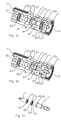
- Figure 1 a is a partial cross-section isometric view of an exemplary embodiment of the invention, demonstrating mating ends with concentric circular folds of equal depth.
- Figure 1b is another partial cross-section isometric view of figure 1a with a portion of the inner conductor, dielectric spacer and an insulator having a 90 degree cut-away.
- Figure 1c is an exploded isometric view of the inner conductor mating ends and dielectric spacer of figure 1a .
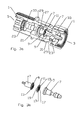
- Figure 2a is a partial cross-section isometric view of an exemplary embodiment of the invention with a portion of the inner conductor, dielectric spacer and an insulator having a 90 degree cut-away, demonstrating mating ends with a concentric circular fold.
- Figure 2b is an exploded isometric view of the inner conductor mating ends and dielectric spacer of figure 2a .
- Figure 3a is a partial cross-section isometric view of an exemplary embodiment of the invention with a portion of the inner conductor, dielectric spacer and an insulator having a 90 degree cut-away, demonstrating mating ends with concentric polygonal folds.
- Figure 3b is an exploded isometric view of the inner conductor mating ends and dielectric spacer of figure 3a .
- Figure 4a is a partial cross-section isometric view of an exemplary embodiment of the invention with a portion of the inner conductor, dielectric spacer and an insulator having a 90 degree cut-away, demonstrating mating ends with radial folds and a conical aspect.
- Figure 4b is an exploded isometric view of the inner conductor mating ends and dielectric spacer of figure 4a .
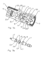
- Figure 5a is a partial cross-section isometric view of an exemplary embodiment of the invention with a portion of the inner conductor, dielectric spacer and an insulator having a 90 degree cut-away, demonstrating mating ends with concentric circular folds in a stepped configuration and a conical aspect.
- Figure 5b is an exploded isometric view of the inner conductor mating ends and dielectric spacer of figure 5a .
- Figure 6a is a partial cross-section isometric view of an exemplary embodiment of the invention with a portion of the inner conductor, dielectric spacer and an insulator having a 90 degree cut-away, demonstrating mating ends with concentric circular folds of unequal depths.
- Figure 6b is an exploded isometric view of the inner conductor mating ends and dielectric spacer of figure 6a .
- an in-line capacitor assembly is shown in figures 1a-6b , for demonstration purposes, the in-line capacitor assembly is demonstrated as a surge suppressor for in-line connection via standardized male and female connection interfaces 1 at first and second ends of the housing 5, 3.
- the in-line capacitor assembly may easily be alternatively configured with additional and or alternative elements for a wide range of different purposes, such as DC-block, DC-bias, bandpass and or interference filtering or the like with any desired standardized or proprietary connection interface(s), including a coaxial cable direct connection interface.
- the inner conductor is provided in two inner conductor segments 7 with mating ends 9 separated by a dielectric spacer 11.
- the inventor has recognized that improvements to the capacitance value and power handling capacity of the in-line capacitor may be realized by increasing the surface area of the mating ends 9.
- the surface area may be increased with a reduced corresponding increase in the required overall length and or diameter of the resulting assembly, by forming the mating surface 15 with folds 13.
- the mating surface 15 folds 13 may be formed as protrusions, corrugations, steps and or ridges. As shown for example in figures 1a-c , folds 13 in the form of corrugations may be formed in concentric circles, the corrugations having peaks and valleys of common depth such that the corrugation peaks of the dielectric spacer 11 front 17 and back 19 are each aligned in generally planar surfaces that are parallel to one another.
- the mating surfaces 15 may also be formed coaxial and or normal with respect to a longitudinal axis of the inner conductor segments 7.
- the diameter of the mating surface 15, number of folds 13 and the depth of each fold 13 may each be adjusted to arrive at the desired surface area.
- figures 1 a-c demonstrate a plurality of concentric circular corrugations
- figures 2a-b demonstrate a single concentric corrugation and a peripheral lip of the corrugation depth.
- the reduced outer diameter of the mating surface 15 enabled by the mating surface 15 folds 13 enables, for an equivalent surface area, the surrounding outer conductor and or housing 21 to be formed with a smaller diameter, for example equal or close to that of the interconnecting coaxial cable, minimizing the introduction of impedance discontinuities to the assembly.
- the outer periphery of the mating surface 15, and thereby the dielectric spacer 11 may be formed as a circle to reduce the generation of impedance discontinuities with respect to a circular inner conductor.
- the mating surface 15 folds 13 also provide a significant improvement over a planar mating surface in that the mating surface 15 folds 13 provide a lateral movement interlock between the inner conductor mating surfaces, reducing the necessary dimensions of supporting structures such as insulators 23 between the inner conductor and the enclosing outer conductor or housing 21.
- a rotational interlock function may also be incorporated into the folds 13 by forming one or more of the folds 13 as a rotational key, for example as a polygon or the like as shown in figures 3a-b . Although a hexagon is demonstrated, any number of sides may be applied.
- Another form of rotational interlock, as shown by figures 4a-b is folds 13 formed radially.
- a rotational interlock may be formed as any protrusion, ridge, fold or other surface feature that prevents rotation between the mating surfaces 15.
- Figures 4a-b also demonstrate a generally conical section mating surface 15.
- Figures 5a-b demonstrate another form of a generally conical section mating surface 15 wherein concentric folds are formed as steps rather than between planar surfaces as shown in figures 1 a-3b .
- a generally conical mating surface increases the lateral movement interlock between the mating surfaces 15.
- mating surfaces are demonstrated by figures 6a-b .
- the mating surface 15 has concentric folds 13 of varying depths.
- folds 13 may be formed to provide a range of different surface areas and interlocking features.
- concentric fold mating surface 15 configurations may be easily manufactured via conventional metal machining and or turning equipment, other non-concentric and non-radial mating surface fold configurations may also be applied, such as a protrusion, grid or honeycomb pattern.
- alternatives to conventional single axis metal machining methods such as metal injection molding and or thixotropic metal molding may be cost effectively applied.
- Prior cylindrical and or parallel plate mating surface in-line capacitors typically applied a plastic or polymer such as mylar or polytetrafluoroethylene (PTFE) as the dielectric spacer 11 material.
- PTFE polytetrafluoroethylene
- the dielectric spacer 11 is formed out of a ceramic dielectric material.
- the thermal properties of ceramic dielectric improve power handling, allowing a higher maximum operating temperature.
- Another advantageous property of a ceramic dielectric spacer 11 is that the ceramic material is resistant to compression and or thermal deformation. Thereby, the desired gap between the mating surfaces, the selected thickness of the dielectric spacer 11, may be maintained with a higher level of precision. Additionally, ceramic material has a higher voltage breakdown for a given thickness, thus reducing the potential for arc thru failure of the capacitor.
- a ceramic dielectric spacer 11 according to the invention may be formed by molding and or machining the dielectric spacer to mate with the selected mating surface.
- an in-line capacitor assembly is as a surge suppressor via the addition of an surge element 27 here demonstrated as an inductor, or an inductor of specific length with respect to the desired operating frequency also known as a 1 ⁇ 4 wavelength shorting stub, the surge element 27 coupled between one of the inner conductor segments 7 and the outer conductor or housing 21, that is, the enclosure sidewall or other ground connection.
- the inductor is demonstrated as having multiple loops, enabling application of an inductor with sufficient length and or inductance characteristics, but that does not require an overly large corresponding increase in the overall diameter of the enclosing housing 21.
- the surge element 27 may be formed in any of several well known configurations such as inductors in the form of a linear stub, a planar or helical spiral, spiral variant or loop.
- Other alternative surge elements 27 include varistors and or gas discharge tubes. Design considerations and manufacturing methods for inductors are well known in the art and as such are not further detailed herein.
- the enclosing housing 21 of the in-line capacitor assembly is demonstrated as two mating portions 29 with a permanent swaged interconnection 31.
- the housing 21 mating portions 29 may be formed with alternative mating means such as complementary threads of the mating portions 29 or alternatively as a single integral cylindrical outer conductor element.
- Shoulders 33 may be formed in the inner diameter of each mating portion 29 to seat the insulators 23 that retain the inner conductor segments 7 coaxial with the housing 21.
- the shoulders 33 may also be used to initially locate each of the inner conductor segment 7 mating surfaces 15 at the correct spacing to achieve the desired mating surface 15 gap, a secure fit of the mating surfaces 15 on either side of the dielectric spacer 11, when the mating portions 29 are mated together.
- an in-line capacitor according to the invention represents significant improvements over the prior art, the improvements potentially including increased power handling capability, increased capacitance, lateral and or rotational inner conductor interlocking, reduction of impedance discontinuities, reduction of overall assembly materials requirements, reduction of overall assembly weight and reduction of overall assembly dimensions.
Landscapes
- Engineering & Computer Science (AREA)
- Power Engineering (AREA)
- Manufacturing & Machinery (AREA)
- Microelectronics & Electronic Packaging (AREA)
- Chemical & Material Sciences (AREA)
- Ceramic Engineering (AREA)
- Inorganic Chemistry (AREA)
- Coupling Device And Connection With Printed Circuit (AREA)
- Fixed Capacitors And Capacitor Manufacturing Machines (AREA)
- Filters And Equalizers (AREA)
- Details Of Connecting Devices For Male And Female Coupling (AREA)
Abstract
Description
- The invention generally relates to inline capacitors. More particularly, the invention relates to a compact coaxial in-line capacitor assembly.
- Electrical cables, for example the coaxial transmission lines interconnecting transceiver equipment with antenna towers, are equipped with surge suppression equipment to provide an electrical path to ground for diversion of electrical current surges resulting from, for example, static discharge and or lightning strikes.
- In-line surge suppression assemblies typically incorporate a frequency selective shorting element such as an inductive coil or stub between the inner and outer conductors of a coaxial cable. To prevent lower frequency and or direct current from being passed to down line equipment a physical break is inserted in the form of an in-line capacitor. The high frequency capacitive coupling across the capacitor is configured to pass only the desired operating frequencies of the system.
- Prior in-line capacitor assemblies have utilized conventional electronic component packages such as ceramic disc or SMD ceramic chips that are mounted by soldering or adhesive mounting within a cavity of a shielding enclosure. The resulting assemblies have limited power ratings, are fragile, expensive to manufacture and introduce a significant impedance discontinuity to the associated coaxial line. In particular, the adhesives SMD capacitors rely on to maintain their position on the center conductor can soften and shift due to high operating temperatures generated by the RF power passing through the device. Any shift in position can permanently adversely affect the designed capacitance.
- Another prior inline capacitor solution is to form a capacitor of the desired value inline by inserting a dielectric spacer between two mating planar or cylindrical pin into socket mating ends of the inner conductor. The capacitance resulting from these solutions is determined by the dielectric value of the spacer material, the gap distance and surface area of the mating surfaces. The resulting modules make tradeoffs between power handling capability, impedance discontinuity and size. Further, these solutions require significant supporting structure to maintain the alignment of the inner conductor mating surfaces.
- Increases in the number of different simultaneous frequency bands carried by a single coaxial cable, for example for cellular voice and data communications applications, has created demand for compact, inexpensive high power capacity inline capacitors as primary elements of coaxial surge protection and or dc-bias assemblies.
- Competition within the electrical cable, connector and associated accessory industries has focused attention on performance improvements and cost reductions resulting from new materials and manufacturing efficiencies, reduced installation requirements and simplification/overall number of discrete parts reduction.
- Therefore, it is an object of the invention to provide an apparatus that overcomes deficiencies in the prior art.
- The accompanying drawings, which are incorporated in and constitute a part of this specification, illustrate embodiments of the invention and, together with a general description of the invention given above, and the detailed description of the embodiments given below, serve to explain the principles of the invention.
-
Figure 1 a is a partial cross-section isometric view of an exemplary embodiment of the invention, demonstrating mating ends with concentric circular folds of equal depth. -
Figure 1b is another partial cross-section isometric view offigure 1a with a portion of the inner conductor, dielectric spacer and an insulator having a 90 degree cut-away. -
Figure 1c is an exploded isometric view of the inner conductor mating ends and dielectric spacer offigure 1a . -
Figure 2a is a partial cross-section isometric view of an exemplary embodiment of the invention with a portion of the inner conductor, dielectric spacer and an insulator having a 90 degree cut-away, demonstrating mating ends with a concentric circular fold. -
Figure 2b is an exploded isometric view of the inner conductor mating ends and dielectric spacer offigure 2a . -
Figure 3a is a partial cross-section isometric view of an exemplary embodiment of the invention with a portion of the inner conductor, dielectric spacer and an insulator having a 90 degree cut-away, demonstrating mating ends with concentric polygonal folds. -
Figure 3b is an exploded isometric view of the inner conductor mating ends and dielectric spacer offigure 3a . -
Figure 4a is a partial cross-section isometric view of an exemplary embodiment of the invention with a portion of the inner conductor, dielectric spacer and an insulator having a 90 degree cut-away, demonstrating mating ends with radial folds and a conical aspect. -
Figure 4b is an exploded isometric view of the inner conductor mating ends and dielectric spacer offigure 4a . -
Figure 5a is a partial cross-section isometric view of an exemplary embodiment of the invention with a portion of the inner conductor, dielectric spacer and an insulator having a 90 degree cut-away, demonstrating mating ends with concentric circular folds in a stepped configuration and a conical aspect. -
Figure 5b is an exploded isometric view of the inner conductor mating ends and dielectric spacer offigure 5a . -
Figure 6a is a partial cross-section isometric view of an exemplary embodiment of the invention with a portion of the inner conductor, dielectric spacer and an insulator having a 90 degree cut-away, demonstrating mating ends with concentric circular folds of unequal depths. -
Figure 6b is an exploded isometric view of the inner conductor mating ends and dielectric spacer offigure 6a . - Exemplary embodiments of an in-line capacitor assembly are shown in
figures 1a-6b , for demonstration purposes, the in-line capacitor assembly is demonstrated as a surge suppressor for in-line connection via standardized male andfemale connection interfaces 1 at first and second ends of thehousing - The inner conductor is provided in two
inner conductor segments 7 withmating ends 9 separated by adielectric spacer 11. The inventor has recognized that improvements to the capacitance value and power handling capacity of the in-line capacitor may be realized by increasing the surface area of themating ends 9. The surface area may be increased with a reduced corresponding increase in the required overall length and or diameter of the resulting assembly, by forming the mating surface 15 withfolds 13. - The mating surface 15
folds 13 may be formed as protrusions, corrugations, steps and or ridges. As shown for example infigures 1a-c ,folds 13 in the form of corrugations may be formed in concentric circles, the corrugations having peaks and valleys of common depth such that the corrugation peaks of thedielectric spacer 11front 17 andback 19 are each aligned in generally planar surfaces that are parallel to one another. The mating surfaces 15 may also be formed coaxial and or normal with respect to a longitudinal axis of theinner conductor segments 7. - The diameter of the mating surface 15, number of
folds 13 and the depth of eachfold 13 may each be adjusted to arrive at the desired surface area. For example, whilefigures 1 a-c demonstrate a plurality of concentric circular corrugations,figures 2a-b demonstrate a single concentric corrugation and a peripheral lip of the corrugation depth. Compared to the prior planar inline capacitors, the reduced outer diameter of the mating surface 15 enabled by the mating surface 15folds 13 enables, for an equivalent surface area, the surrounding outer conductor and orhousing 21 to be formed with a smaller diameter, for example equal or close to that of the interconnecting coaxial cable, minimizing the introduction of impedance discontinuities to the assembly. Further, the outer periphery of the mating surface 15, and thereby thedielectric spacer 11 may be formed as a circle to reduce the generation of impedance discontinuities with respect to a circular inner conductor. - The mating surface 15
folds 13 also provide a significant improvement over a planar mating surface in that the mating surface 15folds 13 provide a lateral movement interlock between the inner conductor mating surfaces, reducing the necessary dimensions of supporting structures such asinsulators 23 between the inner conductor and the enclosing outer conductor orhousing 21. - A rotational interlock function may also be incorporated into the
folds 13 by forming one or more of thefolds 13 as a rotational key, for example as a polygon or the like as shown infigures 3a-b . Although a hexagon is demonstrated, any number of sides may be applied. Another form of rotational interlock, as shown byfigures 4a-b , isfolds 13 formed radially. One skilled in the art will recognize that a rotational interlock may be formed as any protrusion, ridge, fold or other surface feature that prevents rotation between the mating surfaces 15. -
Figures 4a-b also demonstrate a generally conical section mating surface 15.
Figures 5a-b demonstrate another form of a generally conical section mating surface 15 wherein concentric folds are formed as steps rather than between planar surfaces as shown infigures 1 a-3b . A generally conical mating surface increases the lateral movement interlock between the mating surfaces 15. - Another example of mating surfaces is demonstrated by
figures 6a-b . Here the mating surface 15 hasconcentric folds 13 of varying depths. One skilled in the art will recognize thatfolds 13 may be formed to provide a range of different surface areas and interlocking features. While concentric fold mating surface 15 configurations may be easily manufactured via conventional metal machining and or turning equipment, other non-concentric and non-radial mating surface fold configurations may also be applied, such as a protrusion, grid or honeycomb pattern. For these configurations, alternatives to conventional single axis metal machining methods such as metal injection molding and or thixotropic metal molding may be cost effectively applied. - Prior cylindrical and or parallel plate mating surface in-line capacitors typically applied a plastic or polymer such as mylar or polytetrafluoroethylene (PTFE) as the
dielectric spacer 11 material. Although these materials may be applied in an in-line capacitor according to the invention to minimize cost, the inventor has recognized that a significant increase in power capacity may be achieved if thedielectric spacer 11 is formed out of a ceramic dielectric material. The thermal properties of ceramic dielectric improve power handling, allowing a higher maximum operating temperature. Another advantageous property of a ceramicdielectric spacer 11 is that the ceramic material is resistant to compression and or thermal deformation. Thereby, the desired gap between the mating surfaces, the selected thickness of thedielectric spacer 11, may be maintained with a higher level of precision. Additionally, ceramic material has a higher voltage breakdown for a given thickness, thus reducing the potential for arc thru failure of the capacitor. - A
ceramic dielectric spacer 11 according to the invention may be formed by molding and or machining the dielectric spacer to mate with the selected mating surface. - As shown in
figures 1a-6b , a common use of an in-line capacitor assembly is as a surge suppressor via the addition of ansurge element 27 here demonstrated as an inductor, or an inductor of specific length with respect to the desired operating frequency also known as a ¼ wavelength shorting stub, thesurge element 27 coupled between one of theinner conductor segments 7 and the outer conductor orhousing 21, that is, the enclosure sidewall or other ground connection. The inductor is demonstrated as having multiple loops, enabling application of an inductor with sufficient length and or inductance characteristics, but that does not require an overly large corresponding increase in the overall diameter of the enclosinghousing 21. Alternatively, thesurge element 27 may be formed in any of several well known configurations such as inductors in the form of a linear stub, a planar or helical spiral, spiral variant or loop. Otheralternative surge elements 27 include varistors and or gas discharge tubes. Design considerations and manufacturing methods for inductors are well known in the art and as such are not further detailed herein. - The enclosing
housing 21 of the in-line capacitor assembly is demonstrated as twomating portions 29 with a permanent swagedinterconnection 31. Alternatively, thehousing 21mating portions 29 may be formed with alternative mating means such as complementary threads of themating portions 29 or alternatively as a single integral cylindrical outer conductor element. -
Shoulders 33 may be formed in the inner diameter of eachmating portion 29 to seat theinsulators 23 that retain theinner conductor segments 7 coaxial with thehousing 21. Theshoulders 33 may also be used to initially locate each of theinner conductor segment 7 mating surfaces 15 at the correct spacing to achieve the desired mating surface 15 gap, a secure fit of the mating surfaces 15 on either side of thedielectric spacer 11, when themating portions 29 are mated together. - One skilled in the art will recognize that an in-line capacitor according to the invention represents significant improvements over the prior art, the improvements potentially including increased power handling capability, increased capacitance, lateral and or rotational inner conductor interlocking, reduction of impedance discontinuities, reduction of overall assembly materials requirements, reduction of overall assembly weight and reduction of overall assembly dimensions.
Table of Parts 1 connection interface 3 second end 5 first end 7 inner conductor segment 9 mating end 11 dielectric spacer 13 fold 15 mating surface 17 front 19 back 21 housing 23 insulator 27 surge element 29 mating portion 31 swaged interconnection 33 shoulder - Where in the foregoing description reference has been made to ratios, integers, components or modules having known equivalents then such equivalents are herein incorporated as if individually set forth.
- While the present invention has been illustrated by the description of the embodiments thereof, and while the embodiments have been described in considerable detail, it is not the intention of the applicant to restrict or in any way limit the scope of the appended claims to such detail. Additional advantages and modifications will readily appear to those skilled in the art. Therefore, the invention in its broader aspects is not limited to the specific details, representative apparatus, methods, and illustrative examples shown and described. Accordingly, departures may be made from such details without departure from the spirit or scope of applicant's general inventive concept. Further, it is to be appreciated that improvements and/or modifications may be made thereto without departing from the scope or spirit of the present invention as defined by the following claims.
Claims (23)
- An in-line capacitor, comprising:a pair of inner conductor segments, each of the inner conductor segments having a mating surface; anda dielectric spacer positioned between the mating surfaces;each of the mating surfaces having corresponding folds formed thereon.
- The in-line capacitor of claim, wherein the mating surfaces are coaxial with the inner conductor segments.
- The in-line capacitor of claim 1, wherein the folds create a lateral interlock between the mating surfaces.
- The in-line capacitor of claim 3, wherein the folds are concentric circles.
- The in-line capacitor of claim 1, wherein the folds create a rotational interlock between the mating surfaces.
- The in-line capacitor of claim 5, wherein the folds are radial.
- The in-line capacitor of claim 5, wherein the folds are concentric polygons.
- The in-line capacitor of claim 1, wherein the dielectric spacer is a ceramic material.
- The in-line capacitor of claim 1, wherein the dielectric spacer has folds corresponding to each of the mating surfaces, a gap between the mating surfaces generally equal to a thickness of the dielectric spacer.
- The in-line capacitor of claim 1, wherein the folds are concentric about a center of the mating surface.
- The in-line capacitor of claim 1, wherein the dielectric spacer has corresponding folds of equal depth, a front and a back of the dielectric spacer each aligned with a pair of generally planar surfaces, one generally planar surface passing through a peak dimension of the folds and the other generally planar surface passing through a valley dimension of the folds, the generally planar surfaces parallel to one another.
- The in-line capacitor of claim 11, wherein the dielectric spacer has corresponding folds whereby the dielectric spacer has a generally conical section.
- The in-line capacitor of claim 11, wherein the inner conductor segments are each supported by an insulator coaxial within a cylindrical bore of a surrounding housing.
- The in-line capacitor of claim 11, further including an inductor coupled between one of the inner conductor segments and the housing.
- The in-line capacitor of claim 9, further including a coaxial connection interface at each of a first and a second end of the housing.
- A method for manufacturing an in-line capacitor, comprising the steps of:forming a pair of inner conductor segments, each of the inner conductor segments having a mating surface; andpositioning a dielectric spacer between the mating surfaces;each of the mating surfaces having corresponding folds formed thereon.
- The method of claim 16, further including the step of forming the dielectric spacer from a ceramic material.
- The method of claim 16, further including the step of forming a cylindrical housing and inserting the pair of inner conductor segments and dielectric spacer within the housing.
- The method of claim 16, further including the step of coupling a surge element between one of the inner conductor segments and the housing.
- The method of claim 16, wherein the housing has two portions, the two portions joined together via swaging of one end upon another.
- An in-line capacitor, comprising:a pair of inner conductor segments, each of the inner conductor segments having a mating surface; anda ceramic dielectric spacer positioned between the mating surfaces;each of the mating surfaces having corresponding folds formed thereon; the inner conductor segments and dielectric spacer surrounded coaxially by a housing having coaxial connection interfaces at a first end and at a second end.
- The in-line capacitor of claim 21 further including a surge element coupled between one of the inner conductor segments and the housing.
- The in-line capacitor of claim 21, wherein the folds form a lateral movement interlock between the mating surfaces.
Applications Claiming Priority (1)
| Application Number | Priority Date | Filing Date | Title |
|---|---|---|---|
| US11/624,157 US8174132B2 (en) | 2007-01-17 | 2007-01-17 | Folded surface capacitor in-line assembly |
Publications (2)
| Publication Number | Publication Date |
|---|---|
| EP1947661A1 true EP1947661A1 (en) | 2008-07-23 |
| EP1947661B1 EP1947661B1 (en) | 2010-03-03 |
Family
ID=39149326
Family Applications (1)
| Application Number | Title | Priority Date | Filing Date |
|---|---|---|---|
| EP08000560A Not-in-force EP1947661B1 (en) | 2007-01-17 | 2008-01-14 | In-line capacitor assembly with folded electrode surfaces |
Country Status (9)
| Country | Link |
|---|---|
| US (1) | US8174132B2 (en) |
| EP (1) | EP1947661B1 (en) |
| JP (1) | JP2008199002A (en) |
| CN (1) | CN101261897A (en) |
| AT (1) | ATE459967T1 (en) |
| BR (1) | BRPI0801846A2 (en) |
| CA (1) | CA2617020A1 (en) |
| DE (1) | DE602008000420D1 (en) |
| MX (1) | MX2008000720A (en) |
Cited By (4)
| Publication number | Priority date | Publication date | Assignee | Title |
|---|---|---|---|---|
| WO2012071085A1 (en) * | 2010-11-22 | 2012-05-31 | Andrew Llc | Method and apparatus for radial ultrasonic welding interconnected coaxial connector |
| WO2014046899A1 (en) * | 2012-09-19 | 2014-03-27 | Corning Cable Systems Llc | Integrated surge protection for remote radio head power cable assemblies |
| US11437767B2 (en) | 2010-11-22 | 2022-09-06 | Commscope Technologies Llc | Connector and coaxial cable with molecular bond interconnection |
| US11462843B2 (en) | 2010-11-22 | 2022-10-04 | Commscope Technologies Llc | Ultrasonic weld interconnection coaxial connector and interconnection with coaxial cable |
Families Citing this family (43)
| Publication number | Priority date | Publication date | Assignee | Title |
|---|---|---|---|---|
| US20060183509A1 (en) * | 2005-02-16 | 2006-08-17 | Shuyong Shao | DC power source for an accessory of a portable communication device |
| US7623332B2 (en) * | 2008-01-31 | 2009-11-24 | Commscope, Inc. Of North Carolina | Low bypass fine arrestor |
| US20110003507A1 (en) * | 2008-08-14 | 2011-01-06 | Andrew Llc | Multi-shot Connector Assembly and Method of Manufacture |
| US7607942B1 (en) * | 2008-08-14 | 2009-10-27 | Andrew Llc | Multi-shot coaxial connector and method of manufacture |
| EP2523267A4 (en) * | 2010-01-05 | 2014-12-24 | Mitsubishi Electric Corp | CONNECTORS |
| US8976500B2 (en) * | 2010-05-26 | 2015-03-10 | Transtector Systems, Inc. | DC block RF coaxial devices |
| US8894439B2 (en) | 2010-11-22 | 2014-11-25 | Andrew Llc | Capacitivly coupled flat conductor connector |
| US9768574B2 (en) | 2010-11-22 | 2017-09-19 | Commscope Technologies Llc | Cylindrical surface spin weld apparatus |
| US8876549B2 (en) | 2010-11-22 | 2014-11-04 | Andrew Llc | Capacitively coupled flat conductor connector |
| US9761959B2 (en) | 2010-11-22 | 2017-09-12 | Commscope Technologies Llc | Ultrasonic weld coaxial connector |
| US8622768B2 (en) | 2010-11-22 | 2014-01-07 | Andrew Llc | Connector with capacitively coupled connector interface |
| US8826525B2 (en) | 2010-11-22 | 2014-09-09 | Andrew Llc | Laser weld coaxial connector and interconnection method |
| US8622762B2 (en) | 2010-11-22 | 2014-01-07 | Andrew Llc | Blind mate capacitively coupled connector |
| US8963015B2 (en) * | 2011-01-18 | 2015-02-24 | Fisher Controls International Llc | Capacitor coupled cable shield feedthrough |
| EP2549604A1 (en) * | 2011-07-19 | 2013-01-23 | ABB Technology AG | Conductor arrangement for reducing impact of very fast transients |
| US20130100571A1 (en) * | 2011-10-19 | 2013-04-25 | John Mezzalingua Associates, Inc. | Fully isolated coaxial surge protector |
| WO2013071204A1 (en) * | 2011-11-11 | 2013-05-16 | Andrew Llc | Connector with capacitively coupled connector interface |
| WO2013120101A1 (en) | 2012-02-10 | 2013-08-15 | Transtector Systems, Inc. | Reduced let through voltage transient protection or suppression circuit |
| US9048662B2 (en) | 2012-03-19 | 2015-06-02 | Transtector Systems, Inc. | DC power surge protector |
| US9190837B2 (en) | 2012-05-03 | 2015-11-17 | Transtector Systems, Inc. | Rigid flex electromagnetic pulse protection device |
| US9124093B2 (en) | 2012-09-21 | 2015-09-01 | Transtector Systems, Inc. | Rail surge voltage protector with fail disconnect |
| US9425548B2 (en) * | 2012-11-09 | 2016-08-23 | Commscope Technologies Llc | Resilient coaxial connector interface and method of manufacture |
| US8888528B2 (en) * | 2012-11-09 | 2014-11-18 | Andrew Llc | Dual connector interface for capacitive or conductive coupling |
| US8801460B2 (en) | 2012-11-09 | 2014-08-12 | Andrew Llc | RF shielded capacitively coupled connector |
| US8747152B2 (en) | 2012-11-09 | 2014-06-10 | Andrew Llc | RF isolated capacitively coupled connector |
| US9048527B2 (en) * | 2012-11-09 | 2015-06-02 | Commscope Technologies Llc | Coaxial connector with capacitively coupled connector interface and method of manufacture |
| US8858262B2 (en) * | 2012-12-04 | 2014-10-14 | Genesis Technology Usa, Inc. | F-connector with integrated surge protection |
| JP6144580B2 (en) * | 2013-09-04 | 2017-06-07 | Necソリューションイノベータ株式会社 | Cultivation support device, cultivation support method, and program |
| US20150118897A1 (en) * | 2013-10-24 | 2015-04-30 | Andrew Llc | Coaxial cable and connector with capacitive coupling |
| EP3061162B1 (en) * | 2013-10-24 | 2019-09-04 | CommScope Technologies LLC | Coaxial cable and connector with capacitive coupling |
| US9608343B2 (en) | 2013-10-24 | 2017-03-28 | Commscope Technologies Llc | Coaxial cable and connector with capacitive coupling |
| WO2016010885A1 (en) | 2014-07-15 | 2016-01-21 | Commscope Technologies Llc | Coaxial cable and connector with tuned capacitive coupling |
| US9666958B2 (en) | 2014-12-08 | 2017-05-30 | Commscope Technologies Llc | Capacitively coupled connector junctions having parallel signal paths and related connectors and methods |
| US10129993B2 (en) | 2015-06-09 | 2018-11-13 | Transtector Systems, Inc. | Sealed enclosure for protecting electronics |
| US10356928B2 (en) | 2015-07-24 | 2019-07-16 | Transtector Systems, Inc. | Modular protection cabinet with flexible backplane |
| US9924609B2 (en) | 2015-07-24 | 2018-03-20 | Transtector Systems, Inc. | Modular protection cabinet with flexible backplane |
| US10588236B2 (en) | 2015-07-24 | 2020-03-10 | Transtector Systems, Inc. | Modular protection cabinet with flexible backplane |
| WO2017023676A1 (en) | 2015-08-06 | 2017-02-09 | Commscope Technologies Llc | Dielectric spacer for coaxial cable and connector |
| WO2017075286A1 (en) | 2015-10-27 | 2017-05-04 | Transtector Systems, Inc. | Radio frequency surge protector with matched piston-cylinder cavity shape |
| US9991697B1 (en) | 2016-12-06 | 2018-06-05 | Transtector Systems, Inc. | Fail open or fail short surge protector |
| FR3061813B1 (en) * | 2017-01-06 | 2021-09-10 | Citel | INTEGRATED OVERVOLTAGE PROTECTION COMPONENT, ESPECIALLY FOR A COAXIAL CABLE SYSTEM |
| TWM590813U (en) * | 2019-06-14 | 2020-02-11 | 光紅建聖股份有限公司 | Circuit device |
| DE102022201723A1 (en) * | 2022-02-18 | 2023-08-24 | Franz Binder GmbH & Co Elektrische Bauelemente Kommanditgesellschaft | Electrical connector, contact insert and method for manufacturing an electrical connector |
Citations (3)
| Publication number | Priority date | Publication date | Assignee | Title |
|---|---|---|---|---|
| DE4238328A1 (en) * | 1992-11-13 | 1994-05-19 | Bosch Gmbh Robert | Capacitive separator for HF coaxial cable link - provides galvanic isolation of cable outer and inner conductors by capacitors and ferrite-loaded section of semi-rigid cable |
| US6496353B1 (en) | 2002-01-30 | 2002-12-17 | Anritsu Company | Capacitive structure for use with coaxial transmission cables |
| JP2005085721A (en) * | 2003-09-11 | 2005-03-31 | Honda Tsushin Kogyo Co Ltd | Coaxial connector |
Family Cites Families (43)
| Publication number | Priority date | Publication date | Assignee | Title |
|---|---|---|---|---|
| US2516529A (en) | 1946-03-04 | 1950-07-25 | Richard C Raymond | Capacitive connection for coaxial lines |
| US3617607A (en) | 1970-07-10 | 1971-11-02 | Us Air Force | Electromagnetic interference shield isolator |
| US3711794A (en) | 1971-10-21 | 1973-01-16 | Gen Electric | Surge suppression transmission means |
| JPS5353906Y2 (en) | 1974-03-28 | 1978-12-23 | ||
| US4187481A (en) * | 1977-12-23 | 1980-02-05 | Bunker Ramo Corporation | EMI Filter connector having RF suppression characteristics |
| US4161763A (en) * | 1978-03-27 | 1979-07-17 | General Electric Company | Compact voltage surge arrester device |
| US4229714A (en) | 1978-12-15 | 1980-10-21 | Rca Corporation | RF Connector assembly with provision for low frequency isolation and RFI reduction |
| US4399419A (en) | 1980-03-20 | 1983-08-16 | Zenith Radio Corporation | Line isolation and interference shielding for a shielded conductor system |
| US4370630A (en) | 1981-05-18 | 1983-01-25 | Zenith Radio Corporation | Isolating connector |
| US4415949A (en) * | 1981-08-24 | 1983-11-15 | Murata Corporation Of America | Air trimmer capacitor |
| US4554608A (en) | 1982-11-15 | 1985-11-19 | Block Roger R | Connector for electromagnetic impulse suppression |
| US4586008A (en) | 1983-11-09 | 1986-04-29 | Michael Raleigh | Fast passive coaxial integrator |
| JPS60137424U (en) | 1984-02-22 | 1985-09-11 | 株式会社村田製作所 | Capacitor with discharge gap |
| DE3508030A1 (en) * | 1985-02-07 | 1986-08-07 | BBC Aktiengesellschaft Brown, Boveri & Cie., Baden, Aargau | Process for producing a surge arrestor using an active resistor core made from a voltage-dependent resistance material based on ZnO, and surge arrestor manufactured according to the process |
| GB8621429D0 (en) | 1986-09-05 | 1987-01-14 | Raychem Pontoise Sa | Circuit protection device |
| US5097315A (en) | 1989-10-05 | 1992-03-17 | Sumitomo Electric Industries, Ltd. | Integrated capacitor disposed over damaged crystal area |
| US5053910A (en) | 1989-10-16 | 1991-10-01 | Perma Power Electronics, Inc. | Surge suppressor for coaxial transmission line |
| US5122921A (en) | 1990-04-26 | 1992-06-16 | Industrial Communication Engineers, Ltd. | Device for electromagnetic static and voltage suppression |
| US5018047A (en) * | 1990-07-20 | 1991-05-21 | American Technical Ceramics Corporation | Adjustable multilayer capacitor |
| JP2722873B2 (en) | 1991-07-29 | 1998-03-09 | 日本電気株式会社 | Semiconductor device and manufacturing method thereof |
| US5278720A (en) | 1991-09-20 | 1994-01-11 | Atlantic Scientific Corp. | Printed circuit-mounted surge suppressor matched to characteristic impedance of high frequency transmission line |
| US5215478A (en) | 1992-05-29 | 1993-06-01 | Amphenol Corporation | Spark gap device |
| US5278525A (en) | 1992-06-11 | 1994-01-11 | John Mezzalingua Assoc. Inc. | Electrical filter with multiple filter sections |
| US5327111A (en) | 1992-09-16 | 1994-07-05 | Westinghouse Electric Corp. | Motion insensitive phase compensated coaxial connector |
| US5304506A (en) | 1993-03-10 | 1994-04-19 | Micron Semiconductor, Inc. | On chip decoupling capacitor |
| US5500629A (en) | 1993-09-10 | 1996-03-19 | Meyer Dennis R | Noise suppressor |
| US5414588A (en) * | 1993-09-20 | 1995-05-09 | The Regents Of The University Of California | High performance capacitors using nano-structure multilayer materials fabrication |
| FR2726118B1 (en) | 1994-10-19 | 1996-12-06 | Girard Francois | SURGE PROTECTION DEVICE |
| US5589707A (en) | 1994-11-07 | 1996-12-31 | International Business Machines Corporation | Multi-surfaced capacitor for storing more charge per horizontal chip area |
| US5745328A (en) | 1997-03-03 | 1998-04-28 | Watkins-Johnson Company | Electromagnetic impulse suppression curcuit |
| US5790361A (en) | 1997-03-31 | 1998-08-04 | The Whitaker Corporation | Coaxial surge protector with impedance matching |
| DE19717802B4 (en) | 1997-04-26 | 2009-09-17 | Dehn + Söhne GmbH + Co KG | radio link |
| US5844766A (en) | 1997-09-09 | 1998-12-01 | Forem S.R.L. | Lightning supression system for tower mounted antenna systems |
| US6061223A (en) | 1997-10-14 | 2000-05-09 | Polyphaser Corporation | Surge suppressor device |
| US6411492B1 (en) * | 2000-05-24 | 2002-06-25 | Conexant Systems, Inc. | Structure and method for fabrication of an improved capacitor |
| CN1255908C (en) | 2000-10-25 | 2006-05-10 | 灏讯有限公司 | Anti-interference filter and lightning current bypass device |
| US6751081B1 (en) | 2000-11-14 | 2004-06-15 | Corning Gilbert Inc. | Surge protected coaxial termination |
| US6683773B2 (en) | 2000-11-30 | 2004-01-27 | John Mezzalingua Associates, Inc. | High voltage surge protection element for use with CATV coaxial cable connectors |
| US6785110B2 (en) | 2001-10-12 | 2004-08-31 | Polyphaser Corporation | Rf surge protection device |
| KR100471164B1 (en) * | 2002-03-26 | 2005-03-09 | 삼성전자주식회사 | Semiconductor device having metal-insulator-metal capacitor and fabrication method thereof |
| SG105003A1 (en) * | 2002-04-15 | 2004-07-30 | Andrew Corp | Surge lightning protection device |
| US6798310B2 (en) | 2003-01-07 | 2004-09-28 | Agilent Technologies, Inc. | Coaxial DC block |
| US7094104B1 (en) * | 2005-05-04 | 2006-08-22 | Andrew Corporation | In-line coaxial circuit assembly |
-
2007
- 2007-01-17 US US11/624,157 patent/US8174132B2/en active Active
-
2008
- 2008-01-07 CA CA002617020A patent/CA2617020A1/en not_active Abandoned
- 2008-01-14 AT AT08000560T patent/ATE459967T1/en not_active IP Right Cessation
- 2008-01-14 DE DE602008000420T patent/DE602008000420D1/en active Active
- 2008-01-14 EP EP08000560A patent/EP1947661B1/en not_active Not-in-force
- 2008-01-15 MX MX2008000720A patent/MX2008000720A/en not_active Application Discontinuation
- 2008-01-17 CN CNA2008100095523A patent/CN101261897A/en active Pending
- 2008-01-17 JP JP2008008477A patent/JP2008199002A/en not_active Withdrawn
- 2008-01-17 BR BRPI0801846-4A patent/BRPI0801846A2/en not_active IP Right Cessation
Patent Citations (3)
| Publication number | Priority date | Publication date | Assignee | Title |
|---|---|---|---|---|
| DE4238328A1 (en) * | 1992-11-13 | 1994-05-19 | Bosch Gmbh Robert | Capacitive separator for HF coaxial cable link - provides galvanic isolation of cable outer and inner conductors by capacitors and ferrite-loaded section of semi-rigid cable |
| US6496353B1 (en) | 2002-01-30 | 2002-12-17 | Anritsu Company | Capacitive structure for use with coaxial transmission cables |
| JP2005085721A (en) * | 2003-09-11 | 2005-03-31 | Honda Tsushin Kogyo Co Ltd | Coaxial connector |
Cited By (11)
| Publication number | Priority date | Publication date | Assignee | Title |
|---|---|---|---|---|
| WO2012071085A1 (en) * | 2010-11-22 | 2012-05-31 | Andrew Llc | Method and apparatus for radial ultrasonic welding interconnected coaxial connector |
| US9728926B2 (en) | 2010-11-22 | 2017-08-08 | Commscope Technologies Llc | Method and apparatus for radial ultrasonic welding interconnected coaxial connector |
| US10355436B2 (en) | 2010-11-22 | 2019-07-16 | Commscope Technologies Llc | Method and apparatus for radial ultrasonic welding interconnected coaxial connector |
| US11437767B2 (en) | 2010-11-22 | 2022-09-06 | Commscope Technologies Llc | Connector and coaxial cable with molecular bond interconnection |
| US11437766B2 (en) | 2010-11-22 | 2022-09-06 | Commscope Technologies Llc | Connector and coaxial cable with molecular bond interconnection |
| US11462843B2 (en) | 2010-11-22 | 2022-10-04 | Commscope Technologies Llc | Ultrasonic weld interconnection coaxial connector and interconnection with coaxial cable |
| US11735874B2 (en) | 2010-11-22 | 2023-08-22 | Commscope Technologies Llc | Connector and coaxial cable with molecular bond interconnection |
| US11757212B2 (en) | 2010-11-22 | 2023-09-12 | Commscope Technologies Llc | Ultrasonic weld interconnection coaxial connector and interconnection with coaxial cable |
| US12100925B2 (en) | 2010-11-22 | 2024-09-24 | Outdoor Wireless Networks LLC | Ultrasonic weld interconnection coaxial connector and interconnection with coaxial cable |
| US12113317B2 (en) | 2010-11-22 | 2024-10-08 | Outdoor Wireless Networks LLC | Connector and coaxial cable with molecular bond interconnection |
| WO2014046899A1 (en) * | 2012-09-19 | 2014-03-27 | Corning Cable Systems Llc | Integrated surge protection for remote radio head power cable assemblies |
Also Published As
| Publication number | Publication date |
|---|---|
| US8174132B2 (en) | 2012-05-08 |
| DE602008000420D1 (en) | 2010-06-02 |
| BRPI0801846A2 (en) | 2008-12-16 |
| CA2617020A1 (en) | 2008-07-17 |
| CN101261897A (en) | 2008-09-10 |
| US20080170346A1 (en) | 2008-07-17 |
| MX2008000720A (en) | 2009-02-23 |
| JP2008199002A (en) | 2008-08-28 |
| ATE459967T1 (en) | 2010-03-15 |
| EP1947661B1 (en) | 2010-03-03 |
Similar Documents
| Publication | Publication Date | Title |
|---|---|---|
| US8174132B2 (en) | Folded surface capacitor in-line assembly | |
| US7609502B2 (en) | Protective device | |
| US6754060B2 (en) | Protective device | |
| EP2088652B1 (en) | Low bypass fine arrestor | |
| EP0978157B1 (en) | Wide-band electromagnetic-pulse conductor | |
| US7092230B2 (en) | Interference filter and lightning conductor device | |
| US20070053130A1 (en) | Offset Planar Coil Coaxial Surge Suppressor | |
| CN1182299A (en) | Combination coaxial surge arrestor/power extractor | |
| KR100569637B1 (en) | Surge Protection Filters and Lightning Rod Devices | |
| EP1780840A2 (en) | Tuned coil coaxial surge suppressor | |
| US20190348804A1 (en) | Integrated component for protecting against overvoltages, in particular for a coaxial-cable system | |
| EP3780018A1 (en) | Filter cable | |
| US7483251B2 (en) | Multiple planar inductive loop surge suppressor | |
| EP2120282A1 (en) | Coaxial impedance matching adapter and method of manufacture | |
| CN216488434U (en) | Low-pass filtering structure and filter | |
| CA2560787A1 (en) | Multiple planar inductor coaxial surge arrestor | |
| CN114243237A (en) | Low-pass filtering structure and filter | |
| US20240322504A1 (en) | Connector with embedded filter | |
| CN118117394A (en) | RF connectors and electronic devices | |
| US20080049368A1 (en) | Overvoltage protection for a coaxial connector | |
| TWM590811U (en) | Signal protection device and cable connector | |
| JP2020036098A (en) | Power conversion device |
Legal Events
| Date | Code | Title | Description |
|---|---|---|---|
| PUAI | Public reference made under article 153(3) epc to a published international application that has entered the european phase |
Free format text: ORIGINAL CODE: 0009012 |
|
| AK | Designated contracting states |
Kind code of ref document: A1 Designated state(s): AT BE BG CH CY CZ DE DK EE ES FI FR GB GR HR HU IE IS IT LI LT LU LV MC MT NL NO PL PT RO SE SI SK TR |
|
| AX | Request for extension of the european patent |
Extension state: AL BA MK RS |
|
| 17P | Request for examination filed |
Effective date: 20081112 |
|
| 17Q | First examination report despatched |
Effective date: 20081219 |
|
| AKX | Designation fees paid |
Designated state(s): AT BE BG CH CY CZ DE DK EE ES FI FR GB GR HR HU IE IS IT LI LT LU LV MC MT NL NO PL PT RO SE SI SK TR |
|
| GRAP | Despatch of communication of intention to grant a patent |
Free format text: ORIGINAL CODE: EPIDOSNIGR1 |
|
| GRAS | Grant fee paid |
Free format text: ORIGINAL CODE: EPIDOSNIGR3 |
|
| GRAA | (expected) grant |
Free format text: ORIGINAL CODE: 0009210 |
|
| AK | Designated contracting states |
Kind code of ref document: B1 Designated state(s): AT BE BG CH CY CZ DE DK EE ES FI FR GB GR HR HU IE IS IT LI LT LU LV MC MT NL NO PL PT RO SE SI SK TR |
|
| REG | Reference to a national code |
Ref country code: GB Ref legal event code: FG4D |
|
| REG | Reference to a national code |
Ref country code: CH Ref legal event code: EP |
|
| PUAC | Information related to the publication of a b1 document modified or deleted |
Free format text: ORIGINAL CODE: 0009299EPPU |
|
| REG | Reference to a national code |
Ref country code: IE Ref legal event code: FG4D |
|
| GRAA | (expected) grant |
Free format text: ORIGINAL CODE: 0009210 |
|
| REG | Reference to a national code |
Ref country code: CH Ref legal event code: PK Free format text: BERICHTIGUNG (ENGL.) |
|
| REF | Corresponds to: |
Ref document number: 602008000420 Country of ref document: DE Date of ref document: 20100204 Kind code of ref document: P |
|
| DB1 | Publication of patent cancelled | ||
| AK | Designated contracting states |
Kind code of ref document: B1 Designated state(s): AT BE BG CH CY CZ DE DK EE ES FI FR GB GR HR HU IE IS IT LI LT LU LV MC MT NL NO PL PT RO SE SI SK TR |
|
| REG | Reference to a national code |
Ref country code: GB Ref legal event code: FG4D |
|
| REG | Reference to a national code |
Ref country code: CH Ref legal event code: EP Ref country code: CH Ref legal event code: PK Free format text: DIE ERTEILUNG VOM 23.12.2009 WURDE VOM EPA WIDERRUFEN. |
|
| PG25 | Lapsed in a contracting state [announced via postgrant information from national office to epo] |
Ref country code: NO Free format text: LAPSE BECAUSE OF FAILURE TO SUBMIT A TRANSLATION OF THE DESCRIPTION OR TO PAY THE FEE WITHIN THE PRESCRIBED TIME-LIMIT Effective date: 20100323 |
|
| REF | Corresponds to: |
Ref document number: 602008000420 Country of ref document: DE Date of ref document: 20100602 Kind code of ref document: P |
|
| REG | Reference to a national code |
Ref country code: NL Ref legal event code: VDEP Effective date: 20100303 |
|
| PG25 | Lapsed in a contracting state [announced via postgrant information from national office to epo] |
Ref country code: BG Free format text: LAPSE BECAUSE OF FAILURE TO SUBMIT A TRANSLATION OF THE DESCRIPTION OR TO PAY THE FEE WITHIN THE PRESCRIBED TIME-LIMIT Effective date: 20100323 Ref country code: LT Free format text: LAPSE BECAUSE OF FAILURE TO SUBMIT A TRANSLATION OF THE DESCRIPTION OR TO PAY THE FEE WITHIN THE PRESCRIBED TIME-LIMIT Effective date: 20100303 Ref country code: IS Free format text: LAPSE BECAUSE OF FAILURE TO SUBMIT A TRANSLATION OF THE DESCRIPTION OR TO PAY THE FEE WITHIN THE PRESCRIBED TIME-LIMIT Effective date: 20100423 Ref country code: ES Free format text: LAPSE BECAUSE OF FAILURE TO SUBMIT A TRANSLATION OF THE DESCRIPTION OR TO PAY THE FEE WITHIN THE PRESCRIBED TIME-LIMIT Effective date: 20100403 |
|
| LTIE | Lt: invalidation of european patent or patent extension |
Effective date: 20100303 |
|
| PG25 | Lapsed in a contracting state [announced via postgrant information from national office to epo] |
Ref country code: PL Free format text: LAPSE BECAUSE OF FAILURE TO SUBMIT A TRANSLATION OF THE DESCRIPTION OR TO PAY THE FEE WITHIN THE PRESCRIBED TIME-LIMIT Effective date: 20100303 Ref country code: LV Free format text: LAPSE BECAUSE OF FAILURE TO SUBMIT A TRANSLATION OF THE DESCRIPTION OR TO PAY THE FEE WITHIN THE PRESCRIBED TIME-LIMIT Effective date: 20100303 Ref country code: AT Free format text: LAPSE BECAUSE OF FAILURE TO SUBMIT A TRANSLATION OF THE DESCRIPTION OR TO PAY THE FEE WITHIN THE PRESCRIBED TIME-LIMIT Effective date: 20100303 Ref country code: SI Free format text: LAPSE BECAUSE OF FAILURE TO SUBMIT A TRANSLATION OF THE DESCRIPTION OR TO PAY THE FEE WITHIN THE PRESCRIBED TIME-LIMIT Effective date: 20100303 |
|
| PG25 | Lapsed in a contracting state [announced via postgrant information from national office to epo] |
Ref country code: NL Free format text: LAPSE BECAUSE OF FAILURE TO SUBMIT A TRANSLATION OF THE DESCRIPTION OR TO PAY THE FEE WITHIN THE PRESCRIBED TIME-LIMIT Effective date: 20100303 Ref country code: GR Free format text: LAPSE BECAUSE OF FAILURE TO SUBMIT A TRANSLATION OF THE DESCRIPTION OR TO PAY THE FEE WITHIN THE PRESCRIBED TIME-LIMIT Effective date: 20100324 Ref country code: EE Free format text: LAPSE BECAUSE OF FAILURE TO SUBMIT A TRANSLATION OF THE DESCRIPTION OR TO PAY THE FEE WITHIN THE PRESCRIBED TIME-LIMIT Effective date: 20100303 Ref country code: CY Free format text: LAPSE BECAUSE OF FAILURE TO SUBMIT A TRANSLATION OF THE DESCRIPTION OR TO PAY THE FEE WITHIN THE PRESCRIBED TIME-LIMIT Effective date: 20100303 |
|
| PG25 | Lapsed in a contracting state [announced via postgrant information from national office to epo] |
Ref country code: CZ Free format text: LAPSE BECAUSE OF FAILURE TO SUBMIT A TRANSLATION OF THE DESCRIPTION OR TO PAY THE FEE WITHIN THE PRESCRIBED TIME-LIMIT Effective date: 20100303 |
|
| PLBE | No opposition filed within time limit |
Free format text: ORIGINAL CODE: 0009261 |
|
| STAA | Information on the status of an ep patent application or granted ep patent |
Free format text: STATUS: NO OPPOSITION FILED WITHIN TIME LIMIT |
|
| PG25 | Lapsed in a contracting state [announced via postgrant information from national office to epo] |
Ref country code: DK Free format text: LAPSE BECAUSE OF FAILURE TO SUBMIT A TRANSLATION OF THE DESCRIPTION OR TO PAY THE FEE WITHIN THE PRESCRIBED TIME-LIMIT Effective date: 20100303 |
|
| 26N | No opposition filed |
Effective date: 20101206 |
|
| PG25 | Lapsed in a contracting state [announced via postgrant information from national office to epo] |
Ref country code: IT Free format text: LAPSE BECAUSE OF FAILURE TO SUBMIT A TRANSLATION OF THE DESCRIPTION OR TO PAY THE FEE WITHIN THE PRESCRIBED TIME-LIMIT Effective date: 20100303 |
|
| REG | Reference to a national code |
Ref country code: IE Ref legal event code: MM4A |
|
| PG25 | Lapsed in a contracting state [announced via postgrant information from national office to epo] |
Ref country code: MT Free format text: LAPSE BECAUSE OF FAILURE TO SUBMIT A TRANSLATION OF THE DESCRIPTION OR TO PAY THE FEE WITHIN THE PRESCRIBED TIME-LIMIT Effective date: 20100303 |
|
| PG25 | Lapsed in a contracting state [announced via postgrant information from national office to epo] |
Ref country code: IE Free format text: LAPSE BECAUSE OF NON-PAYMENT OF DUE FEES Effective date: 20110114 |
|
| REG | Reference to a national code |
Ref country code: CH Ref legal event code: PL |
|
| REG | Reference to a national code |
Ref country code: FR Ref legal event code: ST Effective date: 20120817 |
|
| GBPC | Gb: european patent ceased through non-payment of renewal fee |
Effective date: 20120114 |
|
| REG | Reference to a national code |
Ref country code: FR Ref legal event code: D3 Effective date: 20120919 |
|
| PG25 | Lapsed in a contracting state [announced via postgrant information from national office to epo] |
Ref country code: CH Free format text: LAPSE BECAUSE OF NON-PAYMENT OF DUE FEES Effective date: 20120131 Ref country code: LI Free format text: LAPSE BECAUSE OF NON-PAYMENT OF DUE FEES Effective date: 20120131 Ref country code: GB Free format text: LAPSE BECAUSE OF NON-PAYMENT OF DUE FEES Effective date: 20120114 |
|
| PG25 | Lapsed in a contracting state [announced via postgrant information from national office to epo] |
Ref country code: HR Free format text: LAPSE BECAUSE OF FAILURE TO SUBMIT A TRANSLATION OF THE DESCRIPTION OR TO PAY THE FEE WITHIN THE PRESCRIBED TIME-LIMIT Effective date: 20100303 |
|
| PG25 | Lapsed in a contracting state [announced via postgrant information from national office to epo] |
Ref country code: FR Free format text: LAPSE BECAUSE OF NON-PAYMENT OF DUE FEES Effective date: 20110131 |
|
| PGFP | Annual fee paid to national office [announced via postgrant information from national office to epo] |
Ref country code: DE Payment date: 20130129 Year of fee payment: 6 Ref country code: FR Payment date: 20130211 Year of fee payment: 6 |
|
| PG25 | Lapsed in a contracting state [announced via postgrant information from national office to epo] |
Ref country code: LU Free format text: LAPSE BECAUSE OF NON-PAYMENT OF DUE FEES Effective date: 20100303 Ref country code: SK Free format text: LAPSE BECAUSE OF FAILURE TO SUBMIT A TRANSLATION OF THE DESCRIPTION OR TO PAY THE FEE WITHIN THE PRESCRIBED TIME-LIMIT Effective date: 20110114 |
|
| PG25 | Lapsed in a contracting state [announced via postgrant information from national office to epo] |
Ref country code: FI Free format text: LAPSE BECAUSE OF FAILURE TO SUBMIT A TRANSLATION OF THE DESCRIPTION OR TO PAY THE FEE WITHIN THE PRESCRIBED TIME-LIMIT Effective date: 20100303 Ref country code: MC Free format text: LAPSE BECAUSE OF NON-PAYMENT OF DUE FEES Effective date: 20110131 |
|
| PG25 | Lapsed in a contracting state [announced via postgrant information from national office to epo] |
Ref country code: PT Free format text: LAPSE BECAUSE OF NON-PAYMENT OF DUE FEES Effective date: 20100303 Ref country code: SE Free format text: LAPSE BECAUSE OF FAILURE TO SUBMIT A TRANSLATION OF THE DESCRIPTION OR TO PAY THE FEE WITHIN THE PRESCRIBED TIME-LIMIT Effective date: 20100303 |
|
| PG25 | Lapsed in a contracting state [announced via postgrant information from national office to epo] |
Ref country code: TR Free format text: LAPSE BECAUSE OF FAILURE TO SUBMIT A TRANSLATION OF THE DESCRIPTION OR TO PAY THE FEE WITHIN THE PRESCRIBED TIME-LIMIT Effective date: 20100303 |
|
| PG25 | Lapsed in a contracting state [announced via postgrant information from national office to epo] |
Ref country code: HU Free format text: LAPSE BECAUSE OF FAILURE TO SUBMIT A TRANSLATION OF THE DESCRIPTION OR TO PAY THE FEE WITHIN THE PRESCRIBED TIME-LIMIT Effective date: 20100303 |
|
| PG25 | Lapsed in a contracting state [announced via postgrant information from national office to epo] |
Ref country code: RO Free format text: LAPSE BECAUSE OF FAILURE TO SUBMIT A TRANSLATION OF THE DESCRIPTION OR TO PAY THE FEE WITHIN THE PRESCRIBED TIME-LIMIT Effective date: 20100303 |
|
| REG | Reference to a national code |
Ref country code: DE Ref legal event code: R119 Ref document number: 602008000420 Country of ref document: DE |
|
| PG25 | Lapsed in a contracting state [announced via postgrant information from national office to epo] |
Ref country code: DE Free format text: LAPSE BECAUSE OF NON-PAYMENT OF DUE FEES Effective date: 20140801 |
|
| REG | Reference to a national code |
Ref country code: FR Ref legal event code: ST Effective date: 20140930 |
|
| REG | Reference to a national code |
Ref country code: DE Ref legal event code: R119 Ref document number: 602008000420 Country of ref document: DE Effective date: 20140801 |
|
| PG25 | Lapsed in a contracting state [announced via postgrant information from national office to epo] |
Ref country code: FR Free format text: LAPSE BECAUSE OF NON-PAYMENT OF DUE FEES Effective date: 20140131 |
|
| PG25 | Lapsed in a contracting state [announced via postgrant information from national office to epo] |
Ref country code: BE Free format text: LAPSE BECAUSE OF NON-PAYMENT OF DUE FEES Effective date: 20100303 |