EP1947652A1 - Phase-change memory device with error correction capability - Google Patents
Phase-change memory device with error correction capability Download PDFInfo
- Publication number
- EP1947652A1 EP1947652A1 EP07425569A EP07425569A EP1947652A1 EP 1947652 A1 EP1947652 A1 EP 1947652A1 EP 07425569 A EP07425569 A EP 07425569A EP 07425569 A EP07425569 A EP 07425569A EP 1947652 A1 EP1947652 A1 EP 1947652A1
- Authority
- EP
- European Patent Office
- Prior art keywords
- parity
- data
- pcm cells
- ebb
- read
- Prior art date
- Legal status (The legal status is an assumption and is not a legal conclusion. Google has not performed a legal analysis and makes no representation as to the accuracy of the status listed.)
- Withdrawn
Links
Images


Classifications
-
- B—PERFORMING OPERATIONS; TRANSPORTING
- B01—PHYSICAL OR CHEMICAL PROCESSES OR APPARATUS IN GENERAL
- B01F—MIXING, e.g. DISSOLVING, EMULSIFYING OR DISPERSING
- B01F27/00—Mixers with rotary stirring devices in fixed receptacles; Kneaders
- B01F27/60—Mixers with rotary stirring devices in fixed receptacles; Kneaders with stirrers rotating about a horizontal or inclined axis
- B01F27/70—Mixers with rotary stirring devices in fixed receptacles; Kneaders with stirrers rotating about a horizontal or inclined axis with paddles, blades or arms
-
- B—PERFORMING OPERATIONS; TRANSPORTING
- B01—PHYSICAL OR CHEMICAL PROCESSES OR APPARATUS IN GENERAL
- B01F—MIXING, e.g. DISSOLVING, EMULSIFYING OR DISPERSING
- B01F27/00—Mixers with rotary stirring devices in fixed receptacles; Kneaders
- B01F27/05—Stirrers
- B01F27/11—Stirrers characterised by the configuration of the stirrers
- B01F27/112—Stirrers characterised by the configuration of the stirrers with arms, paddles, vanes or blades
- B01F27/1121—Stirrers characterised by the configuration of the stirrers with arms, paddles, vanes or blades pin-shaped
-
- B—PERFORMING OPERATIONS; TRANSPORTING
- B01—PHYSICAL OR CHEMICAL PROCESSES OR APPARATUS IN GENERAL
- B01F—MIXING, e.g. DISSOLVING, EMULSIFYING OR DISPERSING
- B01F27/00—Mixers with rotary stirring devices in fixed receptacles; Kneaders
- B01F27/05—Stirrers
- B01F27/11—Stirrers characterised by the configuration of the stirrers
- B01F27/114—Helically shaped stirrers, i.e. stirrers comprising a helically shaped band or helically shaped band sections
- B01F27/1144—Helically shaped stirrers, i.e. stirrers comprising a helically shaped band or helically shaped band sections with a plurality of blades following a helical path on a shaft or a blade support
-
- B—PERFORMING OPERATIONS; TRANSPORTING
- B01—PHYSICAL OR CHEMICAL PROCESSES OR APPARATUS IN GENERAL
- B01F—MIXING, e.g. DISSOLVING, EMULSIFYING OR DISPERSING
- B01F33/00—Other mixers; Mixing plants; Combinations of mixers
- B01F33/70—Mixers specially adapted for working at sub- or super-atmospheric pressure, e.g. combined with de-foaming
-
- G—PHYSICS
- G06—COMPUTING OR CALCULATING; COUNTING
- G06F—ELECTRIC DIGITAL DATA PROCESSING
- G06F11/00—Error detection; Error correction; Monitoring
- G06F11/07—Responding to the occurrence of a fault, e.g. fault tolerance
- G06F11/08—Error detection or correction by redundancy in data representation, e.g. by using checking codes
- G06F11/10—Adding special bits or symbols to the coded information, e.g. parity check, casting out 9's or 11's
- G06F11/1008—Adding special bits or symbols to the coded information, e.g. parity check, casting out 9's or 11's in individual solid state devices
- G06F11/1068—Adding special bits or symbols to the coded information, e.g. parity check, casting out 9's or 11's in individual solid state devices in sector programmable memories, e.g. flash disk
-
- G—PHYSICS
- G11—INFORMATION STORAGE
- G11C—STATIC STORES
- G11C13/00—Digital stores characterised by the use of storage elements not covered by groups G11C11/00, G11C23/00, or G11C25/00
- G11C13/02—Digital stores characterised by the use of storage elements not covered by groups G11C11/00, G11C23/00, or G11C25/00 using elements whose operation depends upon chemical change
-
- B—PERFORMING OPERATIONS; TRANSPORTING
- B01—PHYSICAL OR CHEMICAL PROCESSES OR APPARATUS IN GENERAL
- B01F—MIXING, e.g. DISSOLVING, EMULSIFYING OR DISPERSING
- B01F35/00—Accessories for mixers; Auxiliary operations or auxiliary devices; Parts or details of general application
- B01F35/71—Feed mechanisms
- B01F35/715—Feeding the components in several steps, e.g. successive steps
Definitions
- the present invention relates to a phase-change memory device with error correction capability.
- phase-change memory arrays use a class of materials which have the property of changing between two phases having distinct electrical characteristics.
- these materials may change from an amorphous phase, which is disorderly, to a crystalline or polycrystalline phase, which is orderly, and the two phases are associated to considerably different values of resistivity.
- alloys of elements of group VI of the periodic table such as Te or Se
- chalcogenides or chalcogenic materials can advantageously be used in phase-change cells.
- the chalcogenide that currently offers the most promise is formed by a Ge, Sb and Te alloy (Ge2Sb2Te5) and is widely used for storing information in overwritable disks.
- the resistivity varies by two or more orders of magnitude when the material passes from the amorphous phase (more resistive) to the crystalline phase (more conductive) and vice versa.
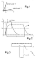
- the characteristics of the chalcogenides in the two phases are shown in Figure 1 .
- Vr read voltage
- Phase change may be obtained by locally increasing the temperature, as shown in Figure 2 . Below 150°C both phases are stable. Above 200°C (nucleation starting temperature Tx), there takes place fast nucleation of the crystallites, and, if the material is kept at the crystallization temperature for a sufficient length of time (time t2), it changes its phase and becomes crystalline. To bring the chalcogenide back into the amorphous state, it is necessary to raise the temperature above the melting temperature Tm (approximately 600°C) and then to cool the chalcogenide off rapidly (time t1).
- Tx melting starting temperature
- phase-change storage element 1 which operates according to the principles described above is shown in Figure 3 and comprises a resistive element 2 (heater) and a programmable element 3.
- the programmable element 3 is made with a chalcogenide and is normally in the crystalline state in order to enable a good flow of current.
- One part of the programmable element 3 is in direct contact with the resistive element 2 and forms a phase-change portion 4.
- phase-change portion 4 If an electric current having an appropriate value is caused to flow through the resistive element 2, it is possible to heat the phase-change portion 4 selectively up to the crystallization temperature or to the melting temperature and to cause phase change.
- the state of the chalcogenic material can be measured by applying a sufficiently small voltage, such as not to cause a sensible heating, and then reading the current flowing. Since the current is proportional to the conductivity of the chalcogenide, it is possible to discriminate wherein state the chalcogenide is.
- the chalcogenide can be electrically switched between different intermediate states, thus affording the possibility of obtaining a multilevel memory.
- phase-change storage element 1 can be considered as a resistor which conducts a different current according to its phase.
- a phase-change storage element is defined as “set” when, once appropriately biased, it conducts a detectable current (this condition may be associated to a logic condition "1”), and as “reset” when, in the same biasing conditions, it does not conduct current or conducts a much lower current than a cell that is set (logic condition "0").
- phase-change storage elements have already been proposed in memory arrays formed by a plurality of memory cells arranged in rows and columns.
- each memory cell comprises a phase-change storage element of the type described above and a selection element (such as an MOS transistor or a diode), coupled to the phase-change storage element.
- read and program errors may occur, on account of a number of events that anyway affect array currents and read/program circuits either temporarily or permanently (such as noise, temperature gradients, external electromagnetic fields, local damages and the like).
- the object of the invention is to provide a phase-change memory device that allows to overcome the limitations described.
- phase-change memory device is provided, as claimed in claim 1.
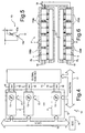
- a phase-change memory device 10 comprises an array 12 of data PCM cells 13, arranged in rows and columns, and is provided with a global row decoder circuit 14 and an error correction module 15.
- Data PCM cells 13 are organized in a plurality of partitions P, that are structurally identical to one another. Partitions P are connected to the global row decoder circuit 14 by respective sets of global word lines 16, one of which is selectively addressed by the global row decoder circuit 14. A group of respective local word lines (not illustrated in figure 4 ) is associated to each global word line 16. Read/program circuits and column decoding circuits are included in each partition P and are not shown in figure 4 , for simplicity.
- An address bus 17 provides the global row decoder circuit 14 and partitions P with addresses of data PCM cells 13 to be read or programmed during read and program operations, respectively.
- a data bus 18 is coupled to the partitions P to collect read data from data PCM cells 13 and to provide data to be stored in data PCM cells 13 during read and program operations, respectively.
- Data stored in the array 12 are encoded according to a known Error Correction Code and therefore include parity bits, as explained later on.
- Data retrieved from the array 12 are sent to the error correction module 15 over the data bus 18.
- the error correction module 15 is configured to restore one error in a page of read data (one bit out of 128 in the embodiment herein described, as will be seen).
- Figure 5 illustrates one exemplar data PCM cell 13 of the array 12. All data PCM cells 13 are identical and include a phase-change memory element 13a and a selector 13b coupled in series thereto.
- the phase-change memory element 13a includes a portion of a phase-change material and is therefore suitable for storing data in form of respective resistance levels associated to different phases of the phase-change material, as above explained.
- the phase-change memory element 13a is illustrated as resistor having variable resistance level.
- the selectors 13b are PNP bipolar transistors controlled to allow currents flow through selected memory elements 13a during read and program operations.
- each partition P comprises two planes PL and a number M of tiles T (M/2 tiles T in each plane PL).
- the number M of tiles T in each partition P is 16.
- Tiles T of each plane PL are aligned along a row direction and are grouped in pairs, to form M/2 elementary building blocks EBB of the array 12 in each partition P.
- Tiles T of the same elementary building block EBB also belong to the same plane PL.
- Tiles T of different planes PL are aligned in pairs along a column direction, perpendicular to the row direction.
- Tiles T of the same partition P share a set of global word lines 16.
- Read/program stages 20 are associated to cells of each partition P.
- Figure 7 shows a pair of adjacent tiles T, that form an elementary building block EBB of the array 12 and may be replicated to form partitions P as required by design specifications.
- Figure 8 shows a single tile T.
- a group of respective local word lines 23 is associated to each global word line 16.
- Tiles T further comprise respective sets of parity PCM cells 25, for storing parity bits associated to data stored in corresponding data PCM cells 13.
- Parity PCM cells 25 have the same structure as data PCM cells 13 and are arranged in parity sections PS, one in each tile T.
- Each parity PCM cells 25 is connected to a respective local word line 23 and to a respective parity bit line 26 ( figure 7 ).
- One local row decoder circuit 27 and one column decoder circuit 28 are associated to each tile T, for selectively connecting one local word line 23 to the respective global word line 16 and for selectively connecting groups of data bit lines 24 and one parity bit line 26 to the respective read/program stages 20, that comprise respective data read/program circuits 20a and parity read/program circuits 20b.
- Tiles T are therefore logically divided into K groups IO and one data bit line 24 in each group IO may be selected for read/program operations by a respective data decoding section 28a the column decoder circuit 28 (e.g. the I-th data bit line 24 in each group IO).
- groups IO are accompanied by a progressive number 0, 1, ..., K-1, in parenthesis.
- an additional parity read/program circuit 20b is shared by the two tiles T forming the same elementary building block EBB and is used for reading and programming the parity PCM cells 25 of the parity sections PS. Since each of the parity has half as many bit lines as groups IO, a single shared parity read/program circuit 20b, identical to data read/program circuits 20a, may be used to read and program parity PCM cells 25 in two adjacent tiles T and a single parity decoding section 28b of the column decoder circuit may be used to address parity bit lines 26 to be connected to the parity read/program circuit 20b. Parity decoding sections 28b are moreover identical to data decoding section 28a.
- phase-change memory device 10 is readable by memory pages of KxM bits from one partition P, where K is the number of data read/program circuits 20a associated to each tile T and M is the number of tiles T in each partition P.
- one parity PCM cell 25 every two tiles T may be addressed and read, so that M/2 parity bits may be associated to each memory page. Hence, correction of one bit in each memory page is available and most reading and programming errors may be corrected.
- Data PCM cells 13 and parity PCM cells 25 may be read simultaneously, thereby providing low access time without appreciably increasing reading noise. It is known that word line leakage is a source of noise and depends on the number of cells that are simultaneously selected on a single local word line 23. In the phase-change memory device 10, only one additional parity PCM cell 25 is selected on an addressed local word line 23. Thus, noise caused by word line leakage is not significantly modified.
- parity sections PS are distributed between all the tiles T of each partition PS, namely the two tiles T of each elementary building block EBB share circuitry required to store one parity bit (parity PCM cells 25, parity bit lines 26 and one additional parity read/program circuit 20b).
- M/2 different tiles are involved in programming as many parity PCM cells 25 and programming may be carried out in a single step.
- Sharing one parity read/program circuit 20b between two parity sections of two tiles T in the same elementary building block EBB provides design simplicity, flexibility and small device size.
- the elementary building blocks EBB may be replicated without any substantial electrical, topological or physical variations (except possibly symmetry: by way of example, elementary building blocks EBB in different planes PL of the same partition P may be specular with respect to one another; however, electrical structure, number and types of components and internal electric connections are unchanged).
- all read/program circuits 20a, 20b are identical, as well as data decoding sections 28a and parity decoding sections 28b of the column decoder circuit 28. Thus, implementing error correction capability does not entail design of special components.
- parity read/program circuits 20b and parity decoding sections 28b of the column decoder circuit 28 are shared between tiles T of the same elementary block EBB so as to be fully exploited. Device area is therefore minimized, in relation to improved error correction capability.
- System 100 may be used in devices such as, for example, a personal digital assistant (PDA), a laptop or portable computer, possibly with wireless capability, a cellphone, a messaging device, a digital music player, a digital camera, or other devices that may be adapted to process, store, transmit or receive information and require permanent storage capability.
- PDA personal digital assistant
- laptop or portable computer possibly with wireless capability
- cellphone a cellphone
- messaging device a digital music player
- digital camera a digital camera
- other devices may be adapted to process, store, transmit or receive information and require permanent storage capability.
- System 100 may include a controller 110, an input/output (I/O) device 120 (e.g. a keyboard, display), the phase-change memory device 10, a wireless interface 140, and a RAM memory 160, coupled to each other via a bus 150.
- I/O input/output
- a battery 180 may be used to supply power to the system 100 in one embodiment. It should be noted that the scope of the present invention is not limited to embodiments having necessarily any or all of above listed components.
- Controller 110 may comprise, for example, one or more microprocessors, digital signal processors, microcontrollers, or the like.
- the I/O device 120 may be used to generate a message.
- the system 100 may use the wireless interface 140 to transmit and receive messages to and from a wireless communication network with a radio frequency (RF) signal.
- RF radio frequency
- Examples of the wireless interface 140 may include an antenna, or a wireless transceiver, such as a dipole antenna, although the scope of the present invention is not limited in this respect.
- the I/O device 120 may deliver a voltage reflecting what is stored as either a digital output (if digital information was stored), or as analog information (if analog information was stored).
Landscapes
- Chemical & Material Sciences (AREA)
- Chemical Kinetics & Catalysis (AREA)
- Engineering & Computer Science (AREA)
- Theoretical Computer Science (AREA)
- Quality & Reliability (AREA)
- Physics & Mathematics (AREA)
- General Engineering & Computer Science (AREA)
- General Physics & Mathematics (AREA)
- Semiconductor Memories (AREA)
- Techniques For Improving Reliability Of Storages (AREA)
- Detection And Correction Of Errors (AREA)
Abstract
A phase-change memory device includes a plurality of data PCM cells (13), for storing data bits; data decoding circuits (14, 27, 28a), for selectively addressing sets of data PCM cells (13); and data read/program circuits (20a), for reading and programming the selected data PCM cells (13). The device further includes a plurality of parity PCM cells (25), for storing parity bits associated to data bits stored in the data PCM cells (13); parity decoding circuits (14, 27, 28b), for selectively addressing sets of parity PCM cells (25); and parity read/program circuits (20b), for reading and programming the selected parity PCM cells (25).
Description
- The present invention relates to a phase-change memory device with error correction capability.
- As is known, phase-change memory arrays use a class of materials which have the property of changing between two phases having distinct electrical characteristics. For example, these materials may change from an amorphous phase, which is disorderly, to a crystalline or polycrystalline phase, which is orderly, and the two phases are associated to considerably different values of resistivity.
- At present, alloys of elements of group VI of the periodic table, such as Te or Se, referred to as chalcogenides or chalcogenic materials, can advantageously be used in phase-change cells. The chalcogenide that currently offers the most promise is formed by a Ge, Sb and Te alloy (Ge2Sb2Te5) and is widely used for storing information in overwritable disks.
- In chalcogenides, the resistivity varies by two or more orders of magnitude when the material passes from the amorphous phase (more resistive) to the crystalline phase (more conductive) and vice versa. The characteristics of the chalcogenides in the two phases are shown in
Figure 1 . As may be noted, at a given read voltage, here designated by Vr, there is a variation in resistance of more than 10. - Phase change may be obtained by locally increasing the temperature, as shown in
Figure 2 . Below 150°C both phases are stable. Above 200°C (nucleation starting temperature Tx), there takes place fast nucleation of the crystallites, and, if the material is kept at the crystallization temperature for a sufficient length of time (time t2), it changes its phase and becomes crystalline. To bring the chalcogenide back into the amorphous state, it is necessary to raise the temperature above the melting temperature Tm (approximately 600°C) and then to cool the chalcogenide off rapidly (time t1). - From the electrical standpoint, it is possible to reach both critical temperatures, namely the crystallization temperature and the melting point, by causing a current to flow through a resistive element which heats the chalcogenic material by Joule effect.
- The basic structure of a phase-
change storage element 1 which operates according to the principles described above is shown inFigure 3 and comprises a resistive element 2 (heater) and aprogrammable element 3. Theprogrammable element 3 is made with a chalcogenide and is normally in the crystalline state in order to enable a good flow of current. One part of theprogrammable element 3 is in direct contact with theresistive element 2 and forms a phase-change portion 4. - If an electric current having an appropriate value is caused to flow through the
resistive element 2, it is possible to heat the phase-change portion 4 selectively up to the crystallization temperature or to the melting temperature and to cause phase change. - The state of the chalcogenic material can be measured by applying a sufficiently small voltage, such as not to cause a sensible heating, and then reading the current flowing. Since the current is proportional to the conductivity of the chalcogenide, it is possible to discriminate wherein state the chalcogenide is.
- Of course, the chalcogenide can be electrically switched between different intermediate states, thus affording the possibility of obtaining a multilevel memory.
- In practice, a phase-
change storage element 1 can be considered as a resistor which conducts a different current according to its phase. In particular, the following convention is adopted: a phase-change storage element is defined as "set" when, once appropriately biased, it conducts a detectable current (this condition may be associated to a logic condition "1"), and as "reset" when, in the same biasing conditions, it does not conduct current or conducts a much lower current than a cell that is set (logic condition "0"). - The use of phase-change storage elements has already been proposed in memory arrays formed by a plurality of memory cells arranged in rows and columns. In order to prevent the memory cells from being affected by noise caused by adjacent memory cells, generally each memory cell comprises a phase-change storage element of the type described above and a selection element (such as an MOS transistor or a diode), coupled to the phase-change storage element.
- Nevertheless, read and program errors may occur, on account of a number of events that anyway affect array currents and read/program circuits either temporarily or permanently (such as noise, temperature gradients, external electromagnetic fields, local damages and the like).
- It would be therefore advisable to implement measures to improve reliability of read and program operations of phase change memory arrays and to reduce errors. Such measures should also comply with general requirements, that are widely felt in the field of microelectronic industry. In particular requirements to minimize device dimensions and power consumption and to simplify array design and layout should be satisfied.
- The object of the invention is to provide a phase-change memory device that allows to overcome the limitations described.
- According to the present invention, a phase-change memory device is provided, as claimed in
claim 1. - For the understanding of the present invention, a preferred embodiment thereof will be now described, purely as non-limitative example, with reference to the enclosed drawings, wherein:
-
figure 1 shows the current-versus-voltage characteristic of a phase-change material; -
figure 2 shows the temperature-versus-current plot of a phase-change material; -
figure 3 shows the basic structure of a phase-change storage element; -
figure 4 shows a simplified block diagram of a phase-change memory device according to the present invention; -
figure 5 is an electric diagram of a phase-change memory cell incorporated in the phase-change memory device offigure 4 ; -
figure 6 is a more detailed block diagram of a portion of the phase-change memory device offigure 4 ; -
figure 7 is a more detailed block diagram of a particular offigure 6 ; -
figure 8 is a more detailed block diagram of a particular offigure 7 ; and -
figure 9 is a system depiction of one embodiment of the present invention. - With reference to
figure 4 , a phase-change memory device 10 comprises anarray 12 ofdata PCM cells 13, arranged in rows and columns, and is provided with a globalrow decoder circuit 14 and anerror correction module 15.Data PCM cells 13 are organized in a plurality of partitions P, that are structurally identical to one another. Partitions P are connected to the globalrow decoder circuit 14 by respective sets ofglobal word lines 16, one of which is selectively addressed by the globalrow decoder circuit 14. A group of respective local word lines (not illustrated infigure 4 ) is associated to eachglobal word line 16. Read/program circuits and column decoding circuits are included in each partition P and are not shown infigure 4 , for simplicity. - An
address bus 17 provides the globalrow decoder circuit 14 and partitions P with addresses ofdata PCM cells 13 to be read or programmed during read and program operations, respectively. Adata bus 18 is coupled to the partitions P to collect read data fromdata PCM cells 13 and to provide data to be stored indata PCM cells 13 during read and program operations, respectively. - Data stored in the
array 12 are encoded according to a known Error Correction Code and therefore include parity bits, as explained later on. Data retrieved from thearray 12 are sent to theerror correction module 15 over thedata bus 18. Theerror correction module 15 is configured to restore one error in a page of read data (one bit out of 128 in the embodiment herein described, as will be seen). -
Figure 5 illustrates one exemplardata PCM cell 13 of thearray 12. Alldata PCM cells 13 are identical and include a phase-change memory element 13a and aselector 13b coupled in series thereto. The phase-change memory element 13a includes a portion of a phase-change material and is therefore suitable for storing data in form of respective resistance levels associated to different phases of the phase-change material, as above explained. Infigure 5 , the phase-change memory element 13a is illustrated as resistor having variable resistance level. In the embodiment herein described, theselectors 13b are PNP bipolar transistors controlled to allow currents flow through selectedmemory elements 13a during read and program operations. - As shown in
Figure 6 ,data PCM cells 13 of each partition P are further organized in planes PL and in tiles T. More precisely, each partition P comprises two planes PL and a number M of tiles T (M/2 tiles T in each plane PL). In the embodiment herein described, the number M of tiles T in each partition P is 16. Tiles T of each plane PL are aligned along a row direction and are grouped in pairs, to form M/2 elementary building blocks EBB of thearray 12 in each partition P. Tiles T of the same elementary building block EBB also belong to the same plane PL. Tiles T of different planes PL are aligned in pairs along a column direction, perpendicular to the row direction. - Tiles T of the same partition P share a set of
global word lines 16. - Read/
program stages 20 are associated to cells of each partition P. - The structure of tiles T will be now illustrated in detail with reference to
figures 7 and8 .Figure 7 shows a pair of adjacent tiles T, that form an elementary building block EBB of thearray 12 and may be replicated to form partitions P as required by design specifications.Figure 8 shows a single tile T. - Each tile T (
figure 8 ) includes NxNdata PCM cells 13, Nlocal word lines 23 and N (local) data bit lines 24 (N = 1024, in the example herein described). A group of respective local word lines 23 is associated to eachglobal word line 16. Tiles T further comprise respective sets of parity PCM cells 25, for storing parity bits associated to data stored in correspondingdata PCM cells 13. Parity PCM cells 25 have the same structure asdata PCM cells 13 and are arranged in parity sections PS, one in each tile T. Each parity PCM cells 25 is connected to a respectivelocal word line 23 and to a respective parity bit line 26 (figure 7 ). - One local
row decoder circuit 27 and onecolumn decoder circuit 28 are associated to each tile T, for selectively connecting onelocal word line 23 to the respectiveglobal word line 16 and for selectively connecting groups of data bitlines 24 and oneparity bit line 26 to the respective read/program stages 20, that comprise respective data read/program circuits 20a and parity read/program circuits 20b. - More precisely, K data read/
program circuits 20a are dedicated to each tile T, and L = 1024/K respective adjacent data bitlines 24 are associated to each data read/program circuit 20a (K = 8 and L = 128 in the embodiment herein described, see alsofigure 8 ). Tiles T are therefore logically divided into K groups IO and onedata bit line 24 in each group IO may be selected for read/program operations by a respectivedata decoding section 28a the column decoder circuit 28 (e.g. the I-th data bitline 24 in each group IO). Infigure 8 , groups IO are accompanied by aprogressive number data PCM cells 13 in each tile T may be simultaneously read, thus leading to an output page of KxM bit read in a single read operation (in the embodiment described, MxK = 128). Due to technological limitations, however, normally only one cell in each tile T is selected for program operation, because higher currents are required. - Each parity section PS also comprises respective (L/2)xN parity PCM cells 25 (64x1024 in the present embodiment) and L/2 parity bit lines 26 (L/2 = 64). Hence, in each parity section PS there are half as many cells and bit lines as in each group IO. Parity bit lines 26 are adjacent to one another and the parity section PS is adjacent to one external group IO of the respective tile T. Moreover, parity sections PS are arranged between the
data PCM cells 13 of the two tiles T in the same elementary building block EBB. - As shown in
figure 7 , an additional parity read/program circuit 20b is shared by the two tiles T forming the same elementary building block EBB and is used for reading and programming the parity PCM cells 25 of the parity sections PS. Since each of the parity has half as many bit lines as groups IO, a single shared parity read/program circuit 20b, identical to data read/program circuits 20a, may be used to read and program parity PCM cells 25 in two adjacent tiles T and a singleparity decoding section 28b of the column decoder circuit may be used to addressparity bit lines 26 to be connected to the parity read/program circuit 20b.Parity decoding sections 28b are moreover identical todata decoding section 28a. - As already mentioned, the phase-
change memory device 10 is readable by memory pages of KxM bits from one partition P, where K is the number of data read/program circuits 20a associated to each tile T and M is the number of tiles T in each partition P. In the embodiment described, in particular, KxM = 128, since K = 8 and M = 16. - In addition, one parity PCM cell 25 every two tiles T may be addressed and read, so that M/2 parity bits may be associated to each memory page. Hence, correction of one bit in each memory page is available and most reading and programming errors may be corrected.
-
Data PCM cells 13 and parity PCM cells 25 may be read simultaneously, thereby providing low access time without appreciably increasing reading noise. It is known that word line leakage is a source of noise and depends on the number of cells that are simultaneously selected on a singlelocal word line 23. In the phase-change memory device 10, only one additional parity PCM cell 25 is selected on an addressedlocal word line 23. Thus, noise caused by word line leakage is not significantly modified. - Also program operation is very fast, because up to M/2 (i.e. eight) parity bits may be simultaneously written in corresponding parity PCM cells 25 of a single partition P. The maximum number of cells of a single tile T that may be simultaneously programmed is normally limited to one by power consumption. In fact, comparatively high currents are required to cause phase transitions and increasing the number of simultaneously programmed cells may lead to damages. However, parity sections PS are distributed between all the tiles T of each partition PS, namely the two tiles T of each elementary building block EBB share circuitry required to store one parity bit (parity PCM cells 25,
parity bit lines 26 and one additional parity read/program circuit 20b). Thus, M/2 different tiles are involved in programming as many parity PCM cells 25 and programming may be carried out in a single step. - Sharing one parity read/
program circuit 20b between two parity sections of two tiles T in the same elementary building block EBB provides design simplicity, flexibility and small device size. On the one side, in fact, the elementary building blocks EBB may be replicated without any substantial electrical, topological or physical variations (except possibly symmetry: by way of example, elementary building blocks EBB in different planes PL of the same partition P may be specular with respect to one another; however, electrical structure, number and types of components and internal electric connections are unchanged). Moreover, all read/program circuits data decoding sections 28a andparity decoding sections 28b of thecolumn decoder circuit 28. Thus, implementing error correction capability does not entail design of special components. On the other side, parity read/program circuits 20b andparity decoding sections 28b of thecolumn decoder circuit 28 are shared between tiles T of the same elementary block EBB so as to be fully exploited. Device area is therefore minimized, in relation to improved error correction capability. - In
Figure 9 , a portion of asystem 100 in accordance with an embodiment of the present invention is illustrated.System 100 may be used in devices such as, for example, a personal digital assistant (PDA), a laptop or portable computer, possibly with wireless capability, a cellphone, a messaging device, a digital music player, a digital camera, or other devices that may be adapted to process, store, transmit or receive information and require permanent storage capability. -
System 100 may include acontroller 110, an input/output (I/O) device 120 (e.g. a keyboard, display), the phase-change memory device 10, awireless interface 140, and aRAM memory 160, coupled to each other via abus 150. Abattery 180 may be used to supply power to thesystem 100 in one embodiment. It should be noted that the scope of the present invention is not limited to embodiments having necessarily any or all of above listed components. -
Controller 110 may comprise, for example, one or more microprocessors, digital signal processors, microcontrollers, or the like. - The I/
O device 120 may be used to generate a message. Thesystem 100 may use thewireless interface 140 to transmit and receive messages to and from a wireless communication network with a radio frequency (RF) signal. Examples of thewireless interface 140 may include an antenna, or a wireless transceiver, such as a dipole antenna, although the scope of the present invention is not limited in this respect. Also, the I/O device 120 may deliver a voltage reflecting what is stored as either a digital output (if digital information was stored), or as analog information (if analog information was stored). - Finally, it is clear that numerous modifications and variations may be made to the device described and illustrated herein, all falling within the scope of the invention, as defined in the attached claims. In particular, the number of tiles T in each partition P, the number of
data reading circuits 20a associated to each tile T and the number of data bitlines 26 in each group IO may change with respect to those described above.
Claims (12)
- A phase-change memory device comprising:a plurality of data PCM cells (13), for storing data bits;data decoding circuits (14, 27, 28a), for selectively addressing sets of data PCM cells (13); anddata read/program circuits (20a), for reading and programming the selected data PCM cells (13);characterized in that it comprises:a plurality of parity PCM cells (25), for storing parity bits associated to data bits stored in the data PCM cells (13);parity decoding circuits (14, 27, 28b), for selectively addressing sets of parity PCM cells (25); andparity read/program circuits (20b), for reading and programming the selected parity PCM cells (25).
- A device according to claim 1, wherein the data PCM cells (13) and the parity PCM cells (25) are organized in a plurality of tiles (T) and each tile (T) includes:a plurality of local word lines (23);a plurality of data bit lines (24), with data PCM cells (13) connected thereto; anda plurality of parity bit lines (26), with parity PCM cells (25) connected thereto.
- A device according to claim 2, wherein the tiles (T) are further organized in a plurality of elementary building blocks (EBB) and each elementary building blocks (EBB) comprises two respective adjacent tiles (T).
- A device according to claim 3, wherein elementary building blocks (EBB) comprise one respective of the parity read/program circuits (20b) each, wherein the parity read/program circuits (20b) are associated to parity bit lines (25) of both tiles (T) of the respective elementary building block (EBB), and wherein the parity decoding circuits (14, 27, 28b) are configured to address parity bit lines (25) of both tiles (T) of each elementary building block (EBB) and to connect selected parity bit lines (25) to the respective parity read/program circuit (20b).
- A device according to claim 3 or 4, wherein all the elementary building blocks (EBB) have identical electrical structure.
- A device according to any one of claims 3 to 5, wherein the elementary building blocks (EBB) further include a predetermined number (K) of data read/program circuits (20a) for each tile (T) of the elementary building blocks (EBB) and each data read/program circuit (20a) is associated to a respective group (IO) of data bit lines (24) of the respective tile (T).
- A device according to claim 6, wherein parity bit lines (26) associated to each tile (T) are half as many as the data bit lines in each group (IO).
- A device according to any one of claims 3 to 7, wherein the elementary building blocks (EBB) further include respective local word line decoding portions (27) of the data decoding circuits (14, 17, 28a) and of the parity decoding circuits (14, 17, 28b).
- A device according to any one of claims 3 to 8, wherein parity PCM cells (25) of each elementary building block (EBB) are arranged between the data PCM cells (13) of the two tiles (T) in the respective elementary building block (EBB).
- A device according to any one of claims 3 to 9, wherein the elementary building blocks (EBB) are further organized in a plurality of partitions (P).
- A device according to any one of the foregoing claims, comprising an error correction module (15).
- A system (100) comprising:a processing unit (110);an interface (140) coupled to the processing unit (110); anda phase-change memory device (10) according to any one of the foregoing claims, coupled to the processing unit (110).
Priority Applications (2)
| Application Number | Priority Date | Filing Date | Title |
|---|---|---|---|
| EP07425569A EP1947652A1 (en) | 2007-09-13 | 2007-09-13 | Phase-change memory device with error correction capability |
| US12/209,967 US7869269B2 (en) | 2007-09-13 | 2008-09-12 | Phase-change memory device with error correction capability |
Applications Claiming Priority (1)
| Application Number | Priority Date | Filing Date | Title |
|---|---|---|---|
| EP07425569A EP1947652A1 (en) | 2007-09-13 | 2007-09-13 | Phase-change memory device with error correction capability |
Publications (2)
| Publication Number | Publication Date |
|---|---|
| EP1947652A1 true EP1947652A1 (en) | 2008-07-23 |
| EP1947652A8 EP1947652A8 (en) | 2009-01-07 |
Family
ID=40262105
Family Applications (1)
| Application Number | Title | Priority Date | Filing Date |
|---|---|---|---|
| EP07425569A Withdrawn EP1947652A1 (en) | 2007-09-13 | 2007-09-13 | Phase-change memory device with error correction capability |
Country Status (2)
| Country | Link |
|---|---|
| US (1) | US7869269B2 (en) |
| EP (1) | EP1947652A1 (en) |
Cited By (2)
| Publication number | Priority date | Publication date | Assignee | Title |
|---|---|---|---|---|
| CN103861505A (en) * | 2014-02-28 | 2014-06-18 | 苏州邦立达新材料有限公司 | Phase change constant-temperature batching device |
| US8964447B2 (en) | 2008-08-13 | 2015-02-24 | Kabushiki Kaisha Toshiba | Nonvolatile semiconductor memory device |
Families Citing this family (9)
| Publication number | Priority date | Publication date | Assignee | Title |
|---|---|---|---|---|
| US8331857B2 (en) * | 2009-05-13 | 2012-12-11 | Micron Technology, Inc. | Wireless interface to program phase-change memories |
| TWI576408B (en) | 2010-08-24 | 2017-04-01 | 精工愛普生股份有限公司 | Film forming ink, film forming method, liquid droplet discharging device, manufacturing method of light emitting element, light emitting element, light emitting device, and electronic device |
| KR101868920B1 (en) | 2011-06-09 | 2018-06-19 | 삼성전자주식회사 | Resistive memory device and therefor method of sensing margin trimming |
| EP2737483A4 (en) * | 2011-07-27 | 2015-05-06 | Hewlett Packard Development Co | Efficient data-storage devices that include memory elements characterized by potentially large switching latencies |
| US9405614B2 (en) | 2011-07-27 | 2016-08-02 | Hewlett Packard Enterprise Development Lp | Method and system for reducing write-buffer capacities within memristor-based data-storage devices |
| US8688954B2 (en) | 2011-08-26 | 2014-04-01 | Microsoft Corporation | Remapping inoperable memory blocks using pointers |
| US8954824B2 (en) * | 2012-02-28 | 2015-02-10 | Micron Technology, Inc. | Error detection or correction of stored signals after one or more heat events in one or more memory devices |
| US9286160B2 (en) | 2014-02-07 | 2016-03-15 | Stmicroelectronics S.R.L. | System and method for phase change memory with erase flag cells |
| CN117711466A (en) * | 2022-07-21 | 2024-03-15 | 长江存储科技有限责任公司 | Memory, operation method thereof and memory system |
Citations (2)
| Publication number | Priority date | Publication date | Assignee | Title |
|---|---|---|---|---|
| US20050055621A1 (en) * | 2003-09-10 | 2005-03-10 | Adelmann Todd Christopher | Magnetic memory with error correction coding |
| EP1708202A2 (en) * | 2005-03-24 | 2006-10-04 | Samsung Electronics Co., Ltd. | Pram device |
Family Cites Families (2)
| Publication number | Priority date | Publication date | Assignee | Title |
|---|---|---|---|---|
| JP4418153B2 (en) * | 2002-12-27 | 2010-02-17 | 株式会社ルネサステクノロジ | Semiconductor device |
| KR100605576B1 (en) * | 2003-12-29 | 2006-07-28 | 주식회사 하이닉스반도체 | Semiconductor memory device capable of maintaining a constant data access timing |
-
2007
- 2007-09-13 EP EP07425569A patent/EP1947652A1/en not_active Withdrawn
-
2008
- 2008-09-12 US US12/209,967 patent/US7869269B2/en active Active
Patent Citations (2)
| Publication number | Priority date | Publication date | Assignee | Title |
|---|---|---|---|---|
| US20050055621A1 (en) * | 2003-09-10 | 2005-03-10 | Adelmann Todd Christopher | Magnetic memory with error correction coding |
| EP1708202A2 (en) * | 2005-03-24 | 2006-10-04 | Samsung Electronics Co., Ltd. | Pram device |
Cited By (7)
| Publication number | Priority date | Publication date | Assignee | Title |
|---|---|---|---|---|
| US8964447B2 (en) | 2008-08-13 | 2015-02-24 | Kabushiki Kaisha Toshiba | Nonvolatile semiconductor memory device |
| US9299426B2 (en) | 2008-08-13 | 2016-03-29 | Kabushiki Kaisha Toshiba | Nonvolatile semiconductor memory device |
| US9543011B2 (en) | 2008-08-13 | 2017-01-10 | Kabushiki Kaisha Toshiba | Nonvolatile semiconductor memory device |
| US9812195B2 (en) | 2008-08-13 | 2017-11-07 | Toshiba Memory Corporation | Nonvolatile semiconductor memory device |
| US10242735B2 (en) | 2008-08-13 | 2019-03-26 | Toshiba Memory Corporation | Nonvolatile semiconductor memory device |
| US11100985B2 (en) | 2008-08-13 | 2021-08-24 | Toshiba Memory Corporation | Nonvolatile semiconductor memory device |
| CN103861505A (en) * | 2014-02-28 | 2014-06-18 | 苏州邦立达新材料有限公司 | Phase change constant-temperature batching device |
Also Published As
| Publication number | Publication date |
|---|---|
| US20090109738A1 (en) | 2009-04-30 |
| EP1947652A8 (en) | 2009-01-07 |
| US7869269B2 (en) | 2011-01-11 |
Similar Documents
| Publication | Publication Date | Title |
|---|---|---|
| US7869269B2 (en) | Phase-change memory device with error correction capability | |
| US9064565B2 (en) | Phase change memory device | |
| EP3509065B1 (en) | A device for switching between different reading modes of a non-volatile memory and method for reading a non-volatile memory | |
| JP2010157316A (en) | Non-volatile memory with ovonic threshold switch | |
| US10593400B2 (en) | Row decoding architecture for a phase-change non-volatile memory device and corresponding row decoding method | |
| US7518934B2 (en) | Phase change memory with program/verify function | |
| US11049561B2 (en) | Method for programming a phase-change memory device of differential type, memory device, and electronic system | |
| US11328768B2 (en) | Phase change memory device, system including the memory device, and method for operating the memory device | |
| US11355191B2 (en) | Method for programming a phase-change memory device of differential type, phase-change memory device, and electronic system | |
| US8934291B2 (en) | Interleaved array architecture |
Legal Events
| Date | Code | Title | Description |
|---|---|---|---|
| PUAI | Public reference made under article 153(3) epc to a published international application that has entered the european phase |
Free format text: ORIGINAL CODE: 0009012 |
|
| AK | Designated contracting states |
Kind code of ref document: A1 Designated state(s): AT BE BG CH CY CZ DE DK EE ES FI FR GB GR HU IE IS IT LI LT LU LV MC MT NL PL PT RO SE SI SK TR |
|
| AX | Request for extension of the european patent |
Extension state: AL BA HR MK RS |
|
| AKX | Designation fees paid | ||
| REG | Reference to a national code |
Ref country code: DE Ref legal event code: 8566 |
|
| STAA | Information on the status of an ep patent application or granted ep patent |
Free format text: STATUS: THE APPLICATION IS DEEMED TO BE WITHDRAWN |
|
| 18D | Application deemed to be withdrawn |
Effective date: 20090124 |