EP1947498A1 - Cofocal microscope - Google Patents
Cofocal microscope Download PDFInfo
- Publication number
- EP1947498A1 EP1947498A1 EP06811846A EP06811846A EP1947498A1 EP 1947498 A1 EP1947498 A1 EP 1947498A1 EP 06811846 A EP06811846 A EP 06811846A EP 06811846 A EP06811846 A EP 06811846A EP 1947498 A1 EP1947498 A1 EP 1947498A1
- Authority
- EP
- European Patent Office
- Prior art keywords
- line
- specific line
- pixel signal
- pixel
- microscope apparatus
- Prior art date
- Legal status (The legal status is an assumption and is not a legal conclusion. Google has not performed a legal analysis and makes no representation as to the accuracy of the status listed.)
- Withdrawn
Links
Images


Classifications
-
- G—PHYSICS
- G02—OPTICS
- G02B—OPTICAL ELEMENTS, SYSTEMS OR APPARATUS
- G02B21/00—Microscopes
- G02B21/0004—Microscopes specially adapted for specific applications
- G02B21/002—Scanning microscopes
- G02B21/0024—Confocal scanning microscopes (CSOMs) or confocal "macroscopes"; Accessories which are not restricted to use with CSOMs, e.g. sample holders
- G02B21/0036—Scanning details, e.g. scanning stages
- G02B21/0048—Scanning details, e.g. scanning stages scanning mirrors, e.g. rotating or galvanomirrors, MEMS mirrors
-
- G—PHYSICS
- G02—OPTICS
- G02B—OPTICAL ELEMENTS, SYSTEMS OR APPARATUS
- G02B21/00—Microscopes
- G02B21/0004—Microscopes specially adapted for specific applications
- G02B21/002—Scanning microscopes
- G02B21/0024—Confocal scanning microscopes (CSOMs) or confocal "macroscopes"; Accessories which are not restricted to use with CSOMs, e.g. sample holders
- G02B21/008—Details of detection or image processing, including general computer control
Definitions
- the present invention relates to a confocal microscope apparatus which detects an image of a specimen line by line.
- a linescanning confocal microscope apparatus illuminates a sample by illuminating light collected in a line shape and detects light generated in an illuminated area on the sample by a light detector such as a one-dimensional CCD (Patent Document 1 or the like).
- a light detector such as a one-dimensional CCD
- Patent Document 1 Japanese Unexamined Patent Application Publication No. 2000-275027
- an object of the present invention is to provide a confocal microscope apparatus capable of obtaining a high confocal effect while detecting an image of a specimen line by line.
- a confocal microscope apparatus of the present invention includes: an illuminating optical system which illuminates a line-shaped area on a specimen plane in a specimen by collected light; an image-forming optical system which forms an image of light emitted from the specimen plane; a two-dimensional light detector which is placed at a conjugate plane of the specimen plane; a scanning unit which moves the line-shaped area on the specimen plane; and a correcting unit which corrects a pixel signal of a specific line on the two-dimensional light detector having a confocal relation with the line-shaped area based on a pixel signal of a peripheral line of the specific line.
- the correcting unit correct a jth pixel signal S (0j) of the specific line L 0 at least based on (j ⁇ 1)th pixel signals S (1,j+1) , S (1,j-1) of a line L 1 shifted by one line from the specific line L 0 .
- the correcting unit may correct the jth pixel signal S (0j) of the specific line L 0 based on (j ⁇ k)th pixel signals S (k,j+k) , S (k,j-k) of a line L k shifted by k lines from the specific line L 0 by a following equation.
- S 0 ⁇ j S 0 ⁇ j - S 1 , j + 1 + S 1 , j - 1 - S 2 , j + 2 + S 2 , j - 2 - ( S 3 , j + 3 + S 3 , j - 3 ) ...
- the correcting unit may correct a jth pixel signal S (0j) of the specific line L 0 at least based on (j ⁇ 1)th pixel signals S (1,j+1) , S (-1,j+1) , S( 1,j-1 ), S (-1,j-1) of two lines L 1 , L 1 shifted by plus or minus one line from the specific line L 0 .
- the correcting unit may correct the jth pixel signal S (0j) of the specific line L 0 based on (j ⁇ k)th pixel signals S (k,j+k) , S (-k,j+k) , S (k,j-k) , S (-k,j-k) of lines L k , L k shifted by plus or minus k lines from the specific line L 0 by a following equation.
- a confocal microscope apparatus capable of obtaining a high confocal effect while detecting an image of a specimen line by line is realized.
- Fig. 1 is an overall configuration diagram of this microscope apparatus. As shown in Fig. 1 , in this microscope apparatus, a laser light source 1, a cylindrical lens 3, a beam splitter 4, a lens 5, a scanner 6, an objective lens 7, a sample (such as an organism sample) 8, a two-dimensional CCD 10, a computer 11, a monitor 12, and so on are placed.
- a laser light source 1 a cylindrical lens 3, a beam splitter 4, a lens 5, a scanner 6, an objective lens 7, a sample (such as an organism sample) 8, a two-dimensional CCD 10, a computer 11, a monitor 12, and so on are placed.
- Laser light 2 emitted from the laser light source 1 is collected in a line shape by the cylindrical lens 3. After passing through the beam splitter 4, the laser light 2 is converted into parallel light by the lens 5, reflected by a scanning mirror 6a in the scanner 6, and collected in a line-shaped area (illuminated area) E on the sample 8 via the objective lens 7. Light generated in the illuminated area E returns to the beam splitter 4 via the objective lens 7, the scanning mirror 6a, and the lens 5. This light is reflected by the beam splitter 4 and forms an image of the illuminated area E at a specific line L 0 on an imaging plane 10a of the two-dimensional CCD 10. The two-dimensional CCD 10 detects a brightness distribution of the imaging plane 10a to generate brightness distribution data and sends it to the computer 11.
- the scanner 6 can change a placement angle of the scanning mirror 6a and moves the illuminated area E on the sample 8 in a short side direction (scanning direction) DS thereof.
- a short side direction scanning direction
- the laser light source 1, the scanner 6, the two-dimensional CCD 10, and so on are controlled by the computer 11.
- the computer 11 performs control processing of controlling the two-dimensional CCD 10 to acquire the brightness distribution data while controlling the scanner 6 to scan the sample 8 in the illuminated area E (details of which will be described later).
- the computer 11 performs arithmetical processing of processing the acquired brightness distribution data to generate a two-dimensional image of the sample 8 (details of which will be described later). Furthermore, the computer 11 also performs conversion processing to display this image on the monitor 12, and the like.
- Fig. 2 is a diagram showing a state in which the sample 8 is illuminated in a magnified form. Illuminating light is collected on a specimen plane 8a in the sample 8 and has spreads in an upper layer and a lower layer of the specimen plane 8a. Hence, hereinafter, the illuminated area E on the specimen plane 8a is particularly called an "illuminated line E".
- Fig. 3 schematically depicts a light path from the sample 8 to the imaging plane 10a. In Figs. 3(A), (B) , states in which the light path is seen from angles different by 90° are shown.
- the imaging plane 10a is located at a conjugate plane of the specimen plane 8a, and the specific line L 0 of the imaging plane 10a has a confocal relation with the illuminated line E.
- Light generated at one point on the illuminated line E is collected on the specific line L 0 and forms an image of the point on one pixel of the specific line L 0 .
- images of respective points on the illuminated line E are formed on respective pixels of the specific line L 0 .
- FIG. 4 is a schematic diagram of the imaging plane 10a viewed from the front.
- the specific line L 0 is located near the center of the imaging plane 10a.
- the specific line L 0 and part of peripheral lines of the specific line are shown in a magnified form.
- a line shifted by i lines from the specific line L 0 is called a "line L 1 ".
- Fig. 5 Shown on the left side of Fig. 5 is a schematic diagram of a section of part of the sample 8, and shown on the right side thereof is a schematic diagram of the imaging plane 10a.
- a light axis direction is represented by the symbol Z
- line directions of the illuminated line E and the specific line L 0 are represented by the symbol DL.
- points A 01 in an upper layer and a lower layer of the point A 00 form a blurred image A 01 ' with the same point as the image Aoo' as its center and cause crosstalk to pixels within its formation range.
- points A 02 in an upper layer and a lower layer of the points A 01 form a more blurred image A 02 ' with the same point as the image Aoo' as its center and cause crosstalk to pixels within its formation range.
- points A 01 , A 02 , ... in an upper layer and a lower layer of the point Aoo form blurred images A 01 , A 02 ', ... with the same point as the image A 00 ' as their center and cause crosstalk to pixels in their formation ranges.
- the more blurred the image the smaller the crosstalk quantity given to one pixel becomes.
- the same goes for a different point on the illuminated line E and points in the upper layer and the lower layer (see Figs. 5(B), (C) ).
- Figs. 5(B), (C) as in Fig. 5(A) , the same subscripts are given to points A in the sample 8 and the images A' on the imaging plane 10a which correspond to each other.
- FIG. 6 attention is paid to some pixel P (0,0) on the specific line L 0 , and only images which affect the pixel P (0,0) are shown.
- P (i,j) is a jth pixel of a line L i .
- the image Aoo' is an image to be detected by the pixel P (0,0) and an image generating a signal component with respect to the pixel P (0,0) .
- the other images A 11 ', A 22 ', A -11 ',A -22 ', ... generate crosstalk components with respect to the pixel P (0,0) .
- the crosstalk quantity given to the pixel P (0,0) by the image A 11 ' is regarded as appearing in a pixel signal of a pixel P (1,1) or a pixel P (-1,1) arranged in an oblique direction with respect to the pixel P (0,0) .
- the crosstalk quantities of the pixels P (1,1) , P (-1,1) received from the image A 11 ' are each the same as that of the pixel P (0,0) .
- the pixels P (1,1) , P (-1,1) exist on lines off the specific line L 0 , and hence have no signal component.
- the crosstalk quantity given to the pixel P (0,0) by the image A- 11 ' is regarded as appearing in a pixel signal of a pixel P (1,1) or a pixel P (-1,-1 ).
- the crosstalk quantity applied to the pixel P (0,0) by the image A 22 ' is regarded as appearing in a pixel signal from a pixel P (2,2) or a pixel P (-2,2) .
- the crosstalk quantity given to the pixel P (0,0) by the image A -22 ' is regarded as appearing in a pixel signal of a pixel P (2,-2) or a pixel P (-2,-2) . Accordingly, pixel signals S (1,1) , S (-1,1) , S (1,-1) S (-1,-1) , S (2,2) , S (-2,2) , S( 2,-2 ), S (-2,-2) , ...
- pixels P (1,1) , P (-1,1) , P (1,-1) P (-1,1) , P (2,2) , P (-2,2) , P (2,-2) , P (-2,-2) , ... represent crosstalk components contained in a pixel signal S (0,0) of the pixel P (0,0) .
- the P (1,1) and the P (-1,1) , the pixel P (1,-1) and the pixel P (-1,-1) , and the like have a symmetrical relation with respect to the specific line L 0 , so that in principle, they should output the same pixel signal. If a difference occurs between the two pixel signals, it is due to the influence of noise. Accordingly, a mean value (mean pixel signal) of the two pixel signals more accurately represents the crosstalk component.
- a general pixel P (0,j) on the specific line L 0 and pixels representing crosstalk components contained in a pixel signal S (0,j) of the pixel P (0,j) are shown using a general pixel number "j".
- an average pixel signal of two pixels symmetrical with respect to the specific line L 0 more accurately represents the crosstalk component.
- a pixel on a line closer to the specific line L 0 represents a more dominant crosstalk component with respect to the pixel P (0,j) .
- Fig. 8 is an operational flowchart of the computer 11. Respective steps will be sequentially described.
- the computer 11 synchronously controls the scanner 6 and the two-dimensional CCD shown in Fig. 1 , and while scanning the sample 8 in the illuminated area E, acquires brightness distribution data when the illuminated area E is on respective lines on the sample 8, respectively (step S1).
- N brightness distribution data acquired here are taken as I 1 , I 2 , I 3 , ..., I N in order of acquisition.
- a specific pixel signal string S 0 contained in each of the brightness distribution data I 1 , I 2 , I 3 , ..., I N is a pixel signal string from the above specific line L 0 .
- Information on lines different from one another on the sample 8 is reflected in the pixel signal string S 0 of the brightness distribution data I 1 , the pixel signal string S 0 of the brightness distribution data I 2 , the pixel signal string S 0 of the brightness distribution data I 2 , ..., the pixel signal string S 0 of the brightness distribution data I N .
- the computer 11 refers to the pixel signal string S 0 of the brightness distribution data I 1 and its peripheral pixel signal strings S 1 , S -1 , S 2 , S -2 , ... and corrects the former based on the latter.
- the pixel signal string S i is a pixel signal string of a line L i
- a pixel signal S (l,j) in the pixel signal string S i is a pixel signal of a pixel P (l,j) .
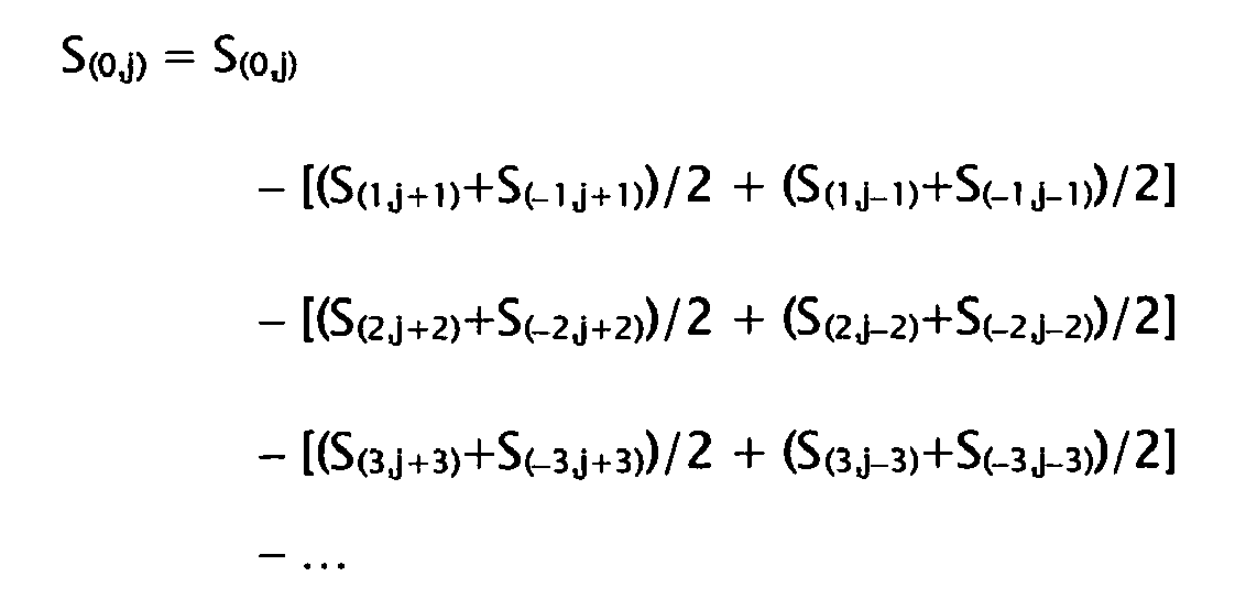
- each pixel signal S (0j) in the pixel signal string S 0 is corrected by the following equation (1).
- S 0 ⁇ j S 0 ⁇ j - S 1 , j + 1 + S - 1 , j + 1 / 2 + ( S 1 , j - 1 + S - 1 , j - 1 / 2 - [ S 2 , j + 2 + S - 2 , j + 2 / 2 + ( S 2 , j - 2 + S - 2 , j - 2 / 2 ]
- each term in square brackets is a correcting term.
- the first correcting term in equation (1) means a correction by four pixels P (1j+1) , P (-1j+1) , P (1j-1 ), P (-1 j-1) on lines L 1 , L 1 shifted by one line from the specific line L 0 (see Fig. 7 ).
- the second correcting term in equation (1) means a correction by four pixels P (2j+2) , P (-2j+2) , P (2j-2 ), P (-2j-2 ) on lines L 2 , L 2 shifted by two lines from the specific line L 0 (see Fig. 7 ).
- the kth correcting term in equation (1) means a correction by four pixels P (k,j+k) , P (-k,j+k) , P (k,j-k) , P (-k,j-k) on lines L k , L k shifted by k lines from the specific line L 0 .
- the first correcting term the most dominant crosstalk components in the pixel signal S (0j) are removed
- the second correcting term the second most dominant crosstalk components in the pixel signal S (0j) are removed
- the kth correcting term the kth most dominant crosstalk components in the pixel signal S (0,j) are removed.
- (S (k,j+k) +S (-k,j+k) /2 in the kth correcting term represents a mean pixel signal of two pixels P (k,j+k) , P (-k,j+k) ) symmetrical with respect to the specific line L 0 . Therefore, according to respective correcting terms in equation (1), various crosstalk components can be removed with high accuracy, respectively.
- the number of correcting terms in equation (1) may be set to a small number such as two or one. This is because the larger kth correcting term (that is, the line more distant from the specific line L 0 ) has a weaker correcting effect.
- the number of correcting terms can be kept low, the number of pixel signal strings to be referred to by the computer 11 in step S2 and arithmetical loading of the computer 11 can be reduced.
- the larger kth correcting term that is, the line more distant from the specific line L 0
- the correcting accuracy may inversely deteriorate. Therefore, it is desirable to select an optimum value as the number of correcting terms by prior experiment, simulation, and so on.
- the computer 11 corrects a pixel signal string S 0 of the brightness distribution data I 2 based on its peripheral pixel signal strings S 1 , S_1, S 2 , S_ 2 , .... Similarly, the computer 11 also corrects pixel signal strings S 0 of the brightness data I 3 , I 4 , I 5 , I 6 , ..., I N .
- the corrected pixel signal string S 0 obtained from the bright data I 1 is replaced with S 10
- the corrected pixel signal string S 0 obtained from the bright data I 2 with S 20 , ..., and the corrected pixel signal string S 0 obtained from the bright data I N with S N0 .
- the computer 11 arranges and combines the corrected pixel signal strings S 10 , S 20 , S 30 , ... S N0 in this order to create one image data I.
- This image data I represents a two-dimensional image of the sample 8.
- this microscope apparatus is a linescanning confocal microscope apparatus, and hence the crosstalk regarding the scanning direction DS does not occur, but the crosstalk regarding the line direction DL occurs.
- a two-dimensional brightness distribution containing not only the specific line L 0 corresponding to the illuminated line E and but also peripheral lines of the specific line is detected, and the former pixel signal is corrected based on the latter pixel signals.
- the crosstalk regarding the line direction DL is suppressed by this correction. Accordingly, this microscope apparatus can obtain a high confocal effect although it is the linescanning one.
- the computer 11 of this microscope apparatus uses the mean pixel signal of two pixels symmetrical with respect to the specific line L 0 in the correction (see equation (1)), so that its correcting accuracy can be increased.
- equation (2) may be used instead of equation (1).
- the first correcting term in equation (2) means a correction by two pixels P (1j+1) , P (1j-1) on L 1 shifted by one line from the specific line L 0 (see Fig. 7 ).
- the second correcting term in equation (2) means a correction by two pixels P (2j+2) , P (2j-2) on the line L 2 shifted by two lines from the specific line L 0 (see Fig. 7 ).
- the kth correcting term in equation (2) means a correction by two pixels P (k,j+k) , P (k,j-k) on the line L k shifted by k lines from the specific line L 0 .
- equation (2) the number of lines used for a correction corresponds to half of that in equation (1).
- arithmetic to calculate the mean pixel signal is not included, so that the speed of correcting arithmetic can be increased.
- the number of correcting terms may be set to a small number such as two or one. This is because the larger kth correcting term (that is, the line more distant from the specific line L 0 ) has a weaker correcting effect. If the number of correcting terms can be kept low, the number of pixel signal strings to be referred to by the computer 11 in step S2 and arithmetical loading of the computer 11 can be reduced.
- the size of the imaging plane 10a when the number of lines used for the correction is small, the size of the imaging plane 10a of the two-dimensional CCD may be correspondingly reduced.
- equation (1) when equation (1) is used as a correcting equation and the number of its correcting terms is two, only four lines are used for the correction, and therefore, the imaging plane 10a has only to have five lines of the specific line L 0 and lines L 1 , L 1 , L 2 , L 2 .
- equation (2) when equation (2) is used as the correcting equation and the number of its correcting terms is two, only two lines are used for the correction, and therefore, the imaging plane 10a has only to have three lines of the specific line L 0 and lines L 1 , L 2 .
- the two-dimensional CCD is used as a two-dimensional light detector, but a different type of two-dimensional light detector may be used as long as it can detect a brightness distribution formed simultaneously in the specific line and peripheral lines of the specific line.
- this microscope apparatus applies the present invention to the linescanning confocal microscope, but even in the case of a spotscanning confocal microscope, the application of the present invention becomes effective as the case may be. It is a case where spotscanning is speeded up and an image of a sample is detected line by line by a charge storage light detector such as a CCD.
- the charge storage light detector detects the time integral of light intensity incident within a finite time period, and hence, even lights incident on different positions on the CCD at different timings cause crosstalk to each other's signals when their incident timings fall within the charge storage period of the CCD.
- the application of the present invention can suppress this crosstalk.
- fluorescence may be observed.
- place a filter as necessary in an appropriate position around the dichroic mirror.
- part or all of processing by the computer 11 of this microscope apparatus may be executed by a circuit instead of the computer 11. The use of the circuit makes it possible to shorten the time until a confocal image is displayed.
Landscapes
- Physics & Mathematics (AREA)
- Chemical & Material Sciences (AREA)
- Analytical Chemistry (AREA)
- General Physics & Mathematics (AREA)
- Optics & Photonics (AREA)
- Engineering & Computer Science (AREA)
- Computer Vision & Pattern Recognition (AREA)
- General Engineering & Computer Science (AREA)
- Microscoopes, Condenser (AREA)
Abstract
Description
- The present invention relates to a confocal microscope apparatus which detects an image of a specimen line by line.
- Generally, a linescanning confocal microscope apparatus illuminates a sample by illuminating light collected in a line shape and detects light generated in an illuminated area on the sample by a light detector such as a one-dimensional CCD (
Patent Document 1 or the like). To acquire a two-dimensional image, it is only required to repeat detection while scanning the sample in the illuminated area. If the detection is performed line by line as just described, the time until two-dimensional image information is acquired can be made shorter than an ordinary confocal microscope apparatus which performs detection point by point. Patent Document 1: Japanese Unexamined Patent Application Publication No.2000-275027 - However, in a linescanning confocal microscope apparatus, crosstalk regarding a short side direction of an illuminated area is suppressed, but crosstalk regarding a longitudinal direction thereof is not suppressed, so that in observation of a sample distributed in the longitudinal direction, a confocal effect (sectioning resolution in a light axis direction and contrast in a planar direction) cannot be obtained.
Hence, an object of the present invention is to provide a confocal microscope apparatus capable of obtaining a high confocal effect while detecting an image of a specimen line by line. - A confocal microscope apparatus of the present invention includes: an illuminating optical system which illuminates a line-shaped area on a specimen plane in a specimen by collected light; an image-forming optical system which forms an image of light emitted from the specimen plane; a two-dimensional light detector which is placed at a conjugate plane of the specimen plane; a scanning unit which moves the line-shaped area on the specimen plane; and a correcting unit which corrects a pixel signal of a specific line on the two-dimensional light detector having a confocal relation with the line-shaped area based on a pixel signal of a peripheral line of the specific line.
- Incidentally, it is desirable that in the peripheral line, at least a line adjacent to the specific line be included.
Further, it is recommended that the correcting unit correct a jth pixel signal S(0j) of the specific line L0 at least based on (j±1)th pixel signals S(1,j+1), S(1,j-1) of a line L1 shifted by one line from the specific line L0. - Furthermore, the correcting unit may correct the jth pixel signal S(0j) of the specific line L0 based on (j±k)th pixel signals S(k,j+k), S(k,j-k) of a line Lk shifted by k lines from the specific line L0 by a following equation.

- Further, the correcting unit may correct a jth pixel signal S(0j) of the specific line L0 at least based on (j±1)th pixel signals S(1,j+1), S(-1,j+1), S(1,j-1), S(-1,j-1) of two lines L1, L1 shifted by plus or minus one line from the specific line L0.
Furthermore, the correcting unit may correct the jth pixel signal S(0j) of the specific line L0 based on (j±k)th pixel signals S(k,j+k), S(-k,j+k), S(k,j-k), S(-k,j-k) of lines Lk, Lk shifted by plus or minus k lines from the specific line L0 by a following equation. -
- According to the present invention, a confocal microscope apparatus capable of obtaining a high confocal effect while detecting an image of a specimen line by line is realized.
-
-
Fig. 1 is an overall configuration diagram of the present microscope apparatus; -
Fig. 2 is a diagram showing a state in which asample 8 is illuminated in a magnified form; -
Fig. 3 schematically depicts a light path from thesample 8 to animaging plane 10a; -
Fig. 4 is a schematic diagram of theimaging plane 10a viewed from the front; -
Fig. 5 is a diagram explaining crosstalk occurring among pixels in a specific line L0; -
Fig. 6 is a diagram showing images which affect some pixel P(0,0) on the specific line L0; -
Fig. 7 is a diagram showing a general pixel P(0j) on the specific line L0 and pixels representing crosstalk components of its pixel signal; and -
Fig. 8 is an operational flowchart of acomputer 11. - An embodiment of the present invention will be described below with reference to the drawings. This embodiment is an embodiment of a confocal microscope apparatus.
First, the overall configuration of this microscope apparatus will be described.
Fig. 1 is an overall configuration diagram of this microscope apparatus. As shown inFig. 1 , in this microscope apparatus, alaser light source 1, acylindrical lens 3, a beam splitter 4, alens 5, ascanner 6, anobjective lens 7, a sample (such as an organism sample) 8, a two-dimensional CCD 10, acomputer 11, amonitor 12, and so on are placed. -
Laser light 2 emitted from thelaser light source 1 is collected in a line shape by thecylindrical lens 3. After passing through the beam splitter 4, thelaser light 2 is converted into parallel light by thelens 5, reflected by ascanning mirror 6a in thescanner 6, and collected in a line-shaped area (illuminated area) E on thesample 8 via theobjective lens 7.
Light generated in the illuminated area E returns to the beam splitter 4 via theobjective lens 7, thescanning mirror 6a, and thelens 5. This light is reflected by the beam splitter 4 and forms an image of the illuminated area E at a specific line L0 on animaging plane 10a of the two-dimensional CCD 10. The two-dimensional CCD 10 detects a brightness distribution of theimaging plane 10a to generate brightness distribution data and sends it to thecomputer 11. - Incidentally, the
scanner 6 can change a placement angle of thescanning mirror 6a and moves the illuminated area E on thesample 8 in a short side direction (scanning direction) DS thereof. When the illuminated area E moves on thesample 8 as just described, an image of a different line on thesample 8 is projected on the specific line L0 of the two-dimensional CCD 10.
Further, thelaser light source 1, thescanner 6, the two-dimensional CCD 10, and so on are controlled by thecomputer 11. For example, thecomputer 11 performs control processing of controlling the two-dimensional CCD 10 to acquire the brightness distribution data while controlling thescanner 6 to scan thesample 8 in the illuminated area E (details of which will be described later). Further, thecomputer 11 performs arithmetical processing of processing the acquired brightness distribution data to generate a two-dimensional image of the sample 8 (details of which will be described later). Furthermore, thecomputer 11 also performs conversion processing to display this image on themonitor 12, and the like. -
Fig. 2 is a diagram showing a state in which thesample 8 is illuminated in a magnified form. Illuminating light is collected on aspecimen plane 8a in thesample 8 and has spreads in an upper layer and a lower layer of thespecimen plane 8a. Hence, hereinafter, the illuminated area E on thespecimen plane 8a is particularly called an "illuminated line E".
Fig. 3 schematically depicts a light path from thesample 8 to theimaging plane 10a. InFigs. 3(A), (B) , states in which the light path is seen from angles different by 90° are shown. - As shown in
Figs. 3(A), (B) , theimaging plane 10a is located at a conjugate plane of thespecimen plane 8a, and the specific line L0 of theimaging plane 10a has a confocal relation with the illuminated line E. Light generated at one point on the illuminated line E is collected on the specific line L0 and forms an image of the point on one pixel of the specific line L0. Namely, images of respective points on the illuminated line E are formed on respective pixels of the specific line L0. - However, in actuality, light (flare) is generated also in lines E' in an upper layer and a lower layer of the illuminated line E. Flare generated at one point on the line E' is collected before or behind the specific line L0, so that an blurred image of the point is formed on plural pixels of the specific line L0. Namely, on the respective pixels of the specific line L0, blurred images of respective points on the line E' are overlappingly formed.
As a result, in each pixel of the specific line L0, crosstalk regarding a scanning direction DS does not occur, but crosstalk regarding a line direction DL occurs. - Next, the crosstalk regarding the line direction DL will be described in detail.
Fig. 4 is a schematic diagram of theimaging plane 10a viewed from the front. As shown inFig. 4 , the specific line L0 is located near the center of theimaging plane 10a. In the lower part ofFig. 4 , the specific line L0 and part of peripheral lines of the specific line are shown in a magnified form. Hereinafter, as shown inFig. 4 , a line shifted by i lines from the specific line L0 is called a "line L1". - Shown on the left side of
Fig. 5 is a schematic diagram of a section of part of thesample 8, and shown on the right side thereof is a schematic diagram of theimaging plane 10a. InFig. 5 , a light axis direction is represented by the symbol Z, and line directions of the illuminated line E and the specific line L0 are represented by the symbol DL.
When some point Aoo on the illuminated line E forms an image Aoo' on a minute circular area on the specific line L0 of theimaging plane 10a as shown inFig. 5(A) , points A01 in an upper layer and a lower layer of the point A00 form a blurred image A01' with the same point as the image Aoo' as its center and cause crosstalk to pixels within its formation range. Further, points A02 in an upper layer and a lower layer of the points A01 form a more blurred image A02' with the same point as the image Aoo' as its center and cause crosstalk to pixels within its formation range. - Namely, points A01, A02, ... in an upper layer and a lower layer of the point Aoo form blurred images A01, A02', ... with the same point as the image A00' as their center and cause crosstalk to pixels in their formation ranges. Incidentally, the more blurred the image, the smaller the crosstalk quantity given to one pixel becomes.
The same goes for a different point on the illuminated line E and points in the upper layer and the lower layer (seeFigs. 5(B), (C) ). InFigs. 5(B), (C) , as inFig. 5(A) , the same subscripts are given to points A in thesample 8 and the images A' on theimaging plane 10a which correspond to each other. - Next, crosstalk components occurring in a pixel signal of the specific line L0 will be described.
InFig. 6 , attention is paid to some pixel P(0,0) on the specific line L0, and only images which affect the pixel P(0,0) are shown. Incidentally, P(i,j) is a jth pixel of a line Li.
As shown inFig. 6 , the image A00' formed on the pixel P(0,0) and images A11', A-11', A22', A-22', ... each of which has its center at a position (mark X) shifted from the pixel P(0,0) in the line direction DL and blurred by its shift quantity affect the pixel P(0,0). - Among them, the image Aoo' is an image to be detected by the pixel P(0,0) and an image generating a signal component with respect to the pixel P(0,0). The other images A11', A22', A-11',A-22', ... generate crosstalk components with respect to the pixel P(0,0).
Here, the crosstalk quantity given to the pixel P(0,0) by the image A11' is regarded as appearing in a pixel signal of a pixel P(1,1) or a pixel P(-1,1) arranged in an oblique direction with respect to the pixel P(0,0). - This is because, firstly, the crosstalk quantities of the pixels P(1,1), P(-1,1) received from the image A11' are each the same as that of the pixel P(0,0). Secondly, the pixels P(1,1), P(-1,1) exist on lines off the specific line L0, and hence have no signal component.
By thinking in the same way, the crosstalk quantity given to the pixel P(0,0) by the image A-11' is regarded as appearing in a pixel signal of a pixel P(1,1) or a pixel P(-1,-1). - Further, the crosstalk quantity applied to the pixel P(0,0) by the image A22' is regarded as appearing in a pixel signal from a pixel P(2,2) or a pixel P(-2,2).
Furthermore, the crosstalk quantity given to the pixel P(0,0) by the image A-22' is regarded as appearing in a pixel signal of a pixel P(2,-2) or a pixel P(-2,-2).
Accordingly, pixel signals S(1,1), S(-1,1), S(1,-1) S(-1,-1), S(2,2), S(-2,2), S(2,-2), S(-2,-2), ... of the pixels P(1,1), P(-1,1), P(1,-1) P(-1,1), P(2,2), P(-2,2), P(2,-2), P(-2,-2), ... represent crosstalk components contained in a pixel signal S(0,0) of the pixel P(0,0). - Incidentally, the P(1,1) and the P(-1,1), the pixel P(1,-1) and the pixel P(-1,-1), and the like have a symmetrical relation with respect to the specific line L0, so that in principle, they should output the same pixel signal. If a difference occurs between the two pixel signals, it is due to the influence of noise. Accordingly, a mean value (mean pixel signal) of the two pixel signals more accurately represents the crosstalk component.
Further, the larger the blur quantity of one image A', the smaller the crosstalk quantity given to one pixel by this image A' becomes, so that out of the pixels P(1,1), P(-1,1), P(1,-1) P(-1,-1), P(2,2), P(-2,2), P(2,-2), P(-2,-2), ..., a pixel on a line closer to the specific line L0 represents a more dominant crosstalk component with respect to the pixel P(0,0). - Moreover, the above description applies to each of pixels on the specific line L0. In
Fig. 7 , a general pixel P(0,j) on the specific line L0 and pixels representing crosstalk components contained in a pixel signal S(0,j) of the pixel P(0,j) are shown using a general pixel number "j". Out of these pixels, an average pixel signal of two pixels symmetrical with respect to the specific line L0 more accurately represents the crosstalk component. Further, a pixel on a line closer to the specific line L0 represents a more dominant crosstalk component with respect to the pixel P(0,j). - Next, based on the above, the operation of the
computer 11 of this microscope apparatus will be described in detail.
Fig. 8 is an operational flowchart of thecomputer 11. Respective steps will be sequentially described. - The
computer 11 synchronously controls thescanner 6 and the two-dimensional CCD shown inFig. 1 , and while scanning thesample 8 in the illuminated area E, acquires brightness distribution data when the illuminated area E is on respective lines on thesample 8, respectively (step S1). N brightness distribution data acquired here are taken as I1, I2, I3, ..., IN in order of acquisition. - A specific pixel signal string S0 contained in each of the brightness distribution data I1, I2, I3, ..., IN is a pixel signal string from the above specific line L0. Information on lines different from one another on the
sample 8 is reflected in the pixel signal string S0 of the brightness distribution data I1, the pixel signal string S0 of the brightness distribution data I2, the pixel signal string S0 of the brightness distribution data I2, ..., the pixel signal string S0 of the brightness distribution data IN. - The
computer 11 refers to the pixel signal string S0 of the brightness distribution data I1 and its peripheral pixel signal strings S1, S-1, S2, S-2, ... and corrects the former based on the latter. Incidentally, the pixel signal string Si is a pixel signal string of a line Li, and a pixel signal S(l,j) in the pixel signal string Si is a pixel signal of a pixel P(l,j). - In this correction, each pixel signal S(0j) in the pixel signal string S0 is corrected by the following equation (1).

- The first correcting term in equation (1) means a correction by four pixels P(1j+1), P(-1j+1), P(1j-1), P(-1 j-1) on lines L1, L1 shifted by one line from the specific line L0 (see
Fig. 7 ).
The second correcting term in equation (1) means a correction by four pixels P(2j+2), P(-2j+2), P(2j-2), P(-2j-2) on lines L2, L2 shifted by two lines from the specific line L0 (seeFig. 7 ). - Similarly, the kth correcting term in equation (1) means a correction by four pixels P(k,j+k), P(-k,j+k), P(k,j-k), P(-k,j-k) on lines Lk, Lk shifted by k lines from the specific line L0.
Hence, according to the first correcting term, the most dominant crosstalk components in the pixel signal S(0j) are removed, according to the second correcting term, the second most dominant crosstalk components in the pixel signal S(0j) are removed, and according to the kth correcting term, the kth most dominant crosstalk components in the pixel signal S(0,j) are removed. - Further, (S(k,j+k)+S(-k,j+k)/2 in the kth correcting term represents a mean pixel signal of two pixels P(k,j+k), P(-k,j+k)) symmetrical with respect to the specific line L0. Therefore, according to respective correcting terms in equation (1), various crosstalk components can be removed with high accuracy, respectively.
Incidentally, the number of correcting terms in equation (1) may be set to a small number such as two or one. This is because the larger kth correcting term (that is, the line more distant from the specific line L0) has a weaker correcting effect. If the number of correcting terms can be kept low, the number of pixel signal strings to be referred to by thecomputer 11 in step S2 and arithmetical loading of thecomputer 11 can be reduced. On the other hand, it is possible in principle to increase the correcting accuracy as the number of correcting terms is increased, but in actuality, the larger kth correcting term (that is, the line more distant from the specific line L0) has worse S/N, and hence if the number of correcting terms is too many, the correcting accuracy may inversely deteriorate. Therefore, it is desirable to select an optimum value as the number of correcting terms by prior experiment, simulation, and so on. - Similarly, the
computer 11 corrects a pixel signal string S0 of the brightness distribution data I2 based on its peripheral pixel signal strings S1, S_1, S2, S_2, .... Similarly, thecomputer 11 also corrects pixel signal strings S0 of the brightness data I3, I4, I5, I6, ..., IN. Incidentally, in this step described above, the corrected pixel signal string S0 obtained from the bright data I1 is replaced with S10, the corrected pixel signal string S0 obtained from the bright data I2 with S20, ..., and the corrected pixel signal string S0 obtained from the bright data IN with SN0. - The
computer 11 arranges and combines the corrected pixel signal strings S10, S20, S30, ... SN0 in this order to create one image data I. This image data I represents a two-dimensional image of thesample 8.
As described above, this microscope apparatus is a linescanning confocal microscope apparatus, and hence the crosstalk regarding the scanning direction DS does not occur, but the crosstalk regarding the line direction DL occurs. However, in this microscope apparatus, a two-dimensional brightness distribution containing not only the specific line L0 corresponding to the illuminated line E and but also peripheral lines of the specific line is detected, and the former pixel signal is corrected based on the latter pixel signals. The crosstalk regarding the line direction DL is suppressed by this correction. Accordingly, this microscope apparatus can obtain a high confocal effect although it is the linescanning one. - Besides, the
computer 11 of this microscope apparatus uses the mean pixel signal of two pixels symmetrical with respect to the specific line L0 in the correction (see equation (1)), so that its correcting accuracy can be increased. - Further, in the correction in step S2, equation (2) may be used instead of equation (1).
-

- The first correcting term in equation (2) means a correction by two pixels P(1j+1), P(1j-1) on L1 shifted by one line from the specific line L0 (see
Fig. 7 ).
The second correcting term in equation (2) means a correction by two pixels P(2j+2), P(2j-2) on the line L2 shifted by two lines from the specific line L0 (seeFig. 7 ).
Similarly, the kth correcting term in equation (2) means a correction by two pixels P(k,j+k), P(k,j-k) on the line Lk shifted by k lines from the specific line L0. - Namely, in equation (2), the number of lines used for a correction corresponds to half of that in equation (1). In this equation (2), arithmetic to calculate the mean pixel signal is not included, so that the speed of correcting arithmetic can be increased.
Incidentally, also when equation (2) is used, the number of correcting terms may be set to a small number such as two or one. This is because the larger kth correcting term (that is, the line more distant from the specific line L0) has a weaker correcting effect. If the number of correcting terms can be kept low, the number of pixel signal strings to be referred to by thecomputer 11 in step S2 and arithmetical loading of thecomputer 11 can be reduced. On the other hand, it is possible in principle to increase the accuracy as the number of correcting terms is increased, but in actuality, the larger kth correcting term (that is, the line more distant from the specific line L0) has worse S/N, and hence if the number of correcting terms is too many, the correcting accuracy may inversely deteriorate. Therefore, it is desirable to select an optimum value as the number of correcting terms by prior experiment, simulation, and so on. - Further, in this embodiment, no mention is made of the size of the
imaging plane 10a, but when the number of lines used for the correction is small, the size of theimaging plane 10a of the two-dimensional CCD may be correspondingly reduced.
For example, when equation (1) is used as a correcting equation and the number of its correcting terms is two, only four lines are used for the correction, and therefore, theimaging plane 10a has only to have five lines of the specific line L0 and lines L1, L1, L2, L2. - Furthermore, when equation (2) is used as the correcting equation and the number of its correcting terms is two, only two lines are used for the correction, and therefore, the
imaging plane 10a has only to have three lines of the specific line L0 and lines L1, L2.
Moreover, in this microscope apparatus, the two-dimensional CCD is used as a two-dimensional light detector, but a different type of two-dimensional light detector may be used as long as it can detect a brightness distribution formed simultaneously in the specific line and peripheral lines of the specific line. - Additionally, this microscope apparatus applies the present invention to the linescanning confocal microscope, but even in the case of a spotscanning confocal microscope, the application of the present invention becomes effective as the case may be. It is a case where spotscanning is speeded up and an image of a sample is detected line by line by a charge storage light detector such as a CCD. The charge storage light detector detects the time integral of light intensity incident within a finite time period, and hence, even lights incident on different positions on the CCD at different timings cause crosstalk to each other's signals when their incident timings fall within the charge storage period of the CCD. However, the application of the present invention can suppress this crosstalk.
- Further, using this microscope apparatus, fluorescence may be observed. For reference's sake, in the fluorescence observation, it is only required to place a sample labeled by a fluorescent material as the
sample 8, place a dichroic mirror as the beam splitter 4, and place a filter as necessary in an appropriate position around the dichroic mirror.
Furthermore, part or all of processing by thecomputer 11 of this microscope apparatus may be executed by a circuit instead of thecomputer 11. The use of the circuit makes it possible to shorten the time until a confocal image is displayed.
Claims (7)
- A confocal microscope apparatus, comprising:an illuminating optical system which illuminates a line-shaped area on a specimen plane in a specimen by collected light;an image-forming optical system which forms an image of light emitted from said specimen plane;a two-dimensional light detector which is placed at a conjugate plane of said specimen plane;a scanning unit which moves said line-shaped area on said specimen plane; anda correcting unit which corrects a pixel signal of a specific line on said two-dimensional light detector having a confocal relation with said line-shaped area based on a pixel signal of a peripheral line of the specific line.
- The confocal microscope apparatus according to claim 1, wherein
in said peripheral line, at least a line adjacent to said specific line is included. - The confocal microscope apparatus according to claim 2, wherein
said correcting unit corrects a jth pixel signal S(0,j) of said specific line L0 at least based on (j±1)th pixel signals S(i,j+1), S(1,j-1) of a line L1 shifted by one line from the specific line L0. - The confocal microscope apparatus according to claim 3, wherein
said correcting unit corrects the jth pixel signal S(0j) of said specific line L0 based on (j±k)th pixel signals S(k,j+k), S(k,j-k) of a line Lk shifted by k lines from said specific line L0 by a following equation.
- The confocal microscope apparatus according to claim 1, wherein
in said peripheral line, at least two lines adjacent to both sides of said specific line are included. - The confocal microscope apparatus according to claim 5, wherein
said correcting unit corrects a jth pixel signal S(0,j) of said specific line L0 at least based on (j±1)th pixel signals S(1,J+1), S(-1,j+1), S(1,j-1), S(-1,j-1) of two lines L1, L1 shifted by plus or minus one line from the specific line L0. - The confocal microscope apparatus according to claim 6, wherein
said correcting unit corrects the jth pixel signal S(0,j) of said specific line L0 based on (j±k)th pixel signals S(k,j+k), S(-k,j+k), S(k,j-k), S(-k,j-k) of lines L+k, Lk shifted by plus or minus k lines from said specific line L0 by a following equation.
Applications Claiming Priority (2)
| Application Number | Priority Date | Filing Date | Title |
|---|---|---|---|
| JP2005327343 | 2005-11-11 | ||
| PCT/JP2006/320589 WO2007055082A1 (en) | 2005-11-11 | 2006-10-16 | Cofocal microscope |
Publications (2)
| Publication Number | Publication Date |
|---|---|
| EP1947498A1 true EP1947498A1 (en) | 2008-07-23 |
| EP1947498A4 EP1947498A4 (en) | 2008-11-19 |
Family
ID=38023089
Family Applications (1)
| Application Number | Title | Priority Date | Filing Date |
|---|---|---|---|
| EP06811846A Withdrawn EP1947498A4 (en) | 2005-11-11 | 2006-10-16 | KOFOKALES MICROSCOPE |
Country Status (4)
| Country | Link |
|---|---|
| US (1) | US8189937B2 (en) |
| EP (1) | EP1947498A4 (en) |
| JP (1) | JP4905356B2 (en) |
| WO (1) | WO2007055082A1 (en) |
Cited By (1)
| Publication number | Priority date | Publication date | Assignee | Title |
|---|---|---|---|---|
| EP3180646A4 (en) * | 2014-08-13 | 2018-04-18 | Daniel Summer Gareau | Line-scanning, sample-scanning, multimodal confocal microscope |
Families Citing this family (5)
| Publication number | Priority date | Publication date | Assignee | Title |
|---|---|---|---|---|
| JP5202936B2 (en) * | 2007-12-14 | 2013-06-05 | オリンパス株式会社 | Scanning microscope |
| JP5921155B2 (en) * | 2011-11-15 | 2016-05-24 | キヤノン株式会社 | Image processing apparatus, image processing method, and computer program |
| WO2018190125A1 (en) * | 2017-04-13 | 2018-10-18 | 横河電機株式会社 | Confocal scanner, microscope system, and confocal microscope |
| JP6677238B2 (en) | 2017-04-13 | 2020-04-08 | 横河電機株式会社 | Confocal scanner and confocal microscope |
| US11237370B2 (en) | 2018-04-30 | 2022-02-01 | University Of Central Florida Research Foundation, Inc. | Multiple inclined beam line-scanning imaging apparatus, methods, and applications |
Family Cites Families (14)
| Publication number | Priority date | Publication date | Assignee | Title |
|---|---|---|---|---|
| JPH01268201A (en) | 1988-04-20 | 1989-10-25 | Toshiba Corp | Planar antenna |
| US5510894A (en) * | 1988-12-22 | 1996-04-23 | Renishaw Plc | Spectroscopic apparatus and methods |
| US5715334A (en) * | 1994-03-08 | 1998-02-03 | The University Of Connecticut | Digital pixel-accurate intensity processing method for image information enhancement |
| JP3869521B2 (en) | 1997-03-24 | 2007-01-17 | オリンパス株式会社 | Scanning laser microscope |
| DE19713362A1 (en) * | 1997-03-29 | 1998-10-01 | Zeiss Carl Jena Gmbh | Confocal microscopic arrangement |
| US5974167A (en) * | 1997-06-30 | 1999-10-26 | M.A.Hannarubbercompounding | System and method for measuring and controlling the quality of dispersion of filler particles in rubber compounds |
| US6388809B1 (en) * | 1997-10-29 | 2002-05-14 | Digital Optical Imaging Corporation | Methods and apparatus for improved depth resolution use of out-of-focus information in microscopy |
| JP4662584B2 (en) * | 1998-01-27 | 2011-03-30 | イーストマン コダック カンパニー | Apparatus and method for removing noise per line of image sensor |
| JP2000275027A (en) | 1999-03-23 | 2000-10-06 | Takaoka Electric Mfg Co Ltd | Slit confocal microscope and surface profile measuring device using it |
| DE10029680B4 (en) * | 2000-06-23 | 2016-06-16 | Leica Microsystems Cms Gmbh | The microscope assemblage |
| CA2445044C (en) * | 2001-04-25 | 2011-02-15 | Amnis Corporation | Method and apparatus for correcting crosstalk and spatial resolution for multichannel imaging |
| JP4280614B2 (en) * | 2003-12-09 | 2009-06-17 | Okiセミコンダクタ株式会社 | Noise reduction circuit and method |
| DE102004034993A1 (en) * | 2004-07-16 | 2006-02-02 | Carl Zeiss Jena Gmbh | Scanning microscope with linear scanning and use |
| US7551799B2 (en) * | 2005-05-13 | 2009-06-23 | Seiko Epson Corporation | Apparatus and method for image noise reduction |
-
2006
- 2006-10-16 US US11/912,830 patent/US8189937B2/en active Active
- 2006-10-16 EP EP06811846A patent/EP1947498A4/en not_active Withdrawn
- 2006-10-16 JP JP2007544077A patent/JP4905356B2/en active Active
- 2006-10-16 WO PCT/JP2006/320589 patent/WO2007055082A1/en not_active Ceased
Cited By (2)
| Publication number | Priority date | Publication date | Assignee | Title |
|---|---|---|---|---|
| EP3180646A4 (en) * | 2014-08-13 | 2018-04-18 | Daniel Summer Gareau | Line-scanning, sample-scanning, multimodal confocal microscope |
| AU2015301585B2 (en) * | 2014-08-13 | 2021-01-07 | Daniel Summer Gareau | Line-scanning, sample-scanning, multimodal confocal microscope |
Also Published As
| Publication number | Publication date |
|---|---|
| WO2007055082A1 (en) | 2007-05-18 |
| JPWO2007055082A1 (en) | 2009-04-30 |
| EP1947498A4 (en) | 2008-11-19 |
| US20090034062A1 (en) | 2009-02-05 |
| US8189937B2 (en) | 2012-05-29 |
| JP4905356B2 (en) | 2012-03-28 |
Similar Documents
| Publication | Publication Date | Title |
|---|---|---|
| EP2136233B1 (en) | Microscope device | |
| US9383563B2 (en) | Confocal image generation apparatus | |
| JP6448996B2 (en) | Microscope system | |
| CN102449527B (en) | Image processing device, image processing method and microscope | |
| US20120075455A1 (en) | Imaging method and microscope device | |
| WO2012096153A1 (en) | Microscope system | |
| CN114442298A (en) | Apparatus and method for capturing image data | |
| JP2010020151A (en) | Observation apparatus | |
| EP2828700A1 (en) | Multi-color confocal microscope and imaging methods | |
| CN121596531A (en) | Microscope, method for determining field inhomogeneity in a field of view of a microscope, and microscopy method | |
| JP2002098901A (en) | Scanning laser microscope | |
| US8189937B2 (en) | Line-scanning confocal microscope apparatus | |
| CN117930497A (en) | Method and apparatus for light field microscopy | |
| US8254019B2 (en) | Confocal microscope apparatus | |
| EP1906224B1 (en) | Confocal Microscope Apparatus | |
| JP4883936B2 (en) | Image processing method and apparatus for scanning cytometer | |
| JPH11231223A (en) | Scanning optical microscope | |
| EP2157466A1 (en) | Confocal microscope device | |
| US7864413B2 (en) | Examination apparatus with multiple image acquisition devices | |
| GB2434651A (en) | A method and apparatus for aligning or superposing microscope images | |
| WO2023189393A1 (en) | Biological sample observation system, information processing device, and image generation method | |
| JP2008051772A (en) | Fluorescence image acquisition device and fluorescence image acquisition method | |
| JP2018116197A (en) | Microscope system, lamination image generation program, and lamination image generation method | |
| CN114363481A (en) | Microscope with device for detecting displacement of sample relative to objective lens and detection method thereof | |
| EP4660683A1 (en) | Image acquisition device and image acquisition method |
Legal Events
| Date | Code | Title | Description |
|---|---|---|---|
| PUAI | Public reference made under article 153(3) epc to a published international application that has entered the european phase |
Free format text: ORIGINAL CODE: 0009012 |
|
| 17P | Request for examination filed |
Effective date: 20071026 |
|
| AK | Designated contracting states |
Kind code of ref document: A1 Designated state(s): AT BE BG CH CY CZ DE DK EE ES FI FR GB GR HU IE IS IT LI LT LU LV MC NL PL PT RO SE SI SK TR |
|
| A4 | Supplementary search report drawn up and despatched |
Effective date: 20081021 |
|
| 17Q | First examination report despatched |
Effective date: 20090213 |
|
| RAP1 | Party data changed (applicant data changed or rights of an application transferred) |
Owner name: NIKON CORPORATION |
|
| DAX | Request for extension of the european patent (deleted) | ||
| RAP1 | Party data changed (applicant data changed or rights of an application transferred) |
Owner name: NIKON CORPORATION |
|
| STAA | Information on the status of an ep patent application or granted ep patent |
Free format text: STATUS: EXAMINATION IS IN PROGRESS |
|
| STAA | Information on the status of an ep patent application or granted ep patent |
Free format text: STATUS: THE APPLICATION IS DEEMED TO BE WITHDRAWN |
|
| 18D | Application deemed to be withdrawn |
Effective date: 20201110 |