EP1946440B1 - A transconductance stage arrangement - Google Patents
A transconductance stage arrangement Download PDFInfo
- Publication number
- EP1946440B1 EP1946440B1 EP05794514A EP05794514A EP1946440B1 EP 1946440 B1 EP1946440 B1 EP 1946440B1 EP 05794514 A EP05794514 A EP 05794514A EP 05794514 A EP05794514 A EP 05794514A EP 1946440 B1 EP1946440 B1 EP 1946440B1
- Authority
- EP
- European Patent Office
- Prior art keywords
- transistor
- transconductance stage
- transistors
- arrangement according
- stage arrangement
- Prior art date
- Legal status (The legal status is an assumption and is not a legal conclusion. Google has not performed a legal analysis and makes no representation as to the accuracy of the status listed.)
- Expired - Lifetime
Links
Images


Classifications
-
- H—ELECTRICITY
- H03—ELECTRONIC CIRCUITRY
- H03F—AMPLIFIERS
- H03F3/00—Amplifiers with only discharge tubes or only semiconductor devices as amplifying elements
- H03F3/45—Differential amplifiers
- H03F3/45071—Differential amplifiers with semiconductor devices only
- H03F3/45076—Differential amplifiers with semiconductor devices only characterised by the way of implementation of the active amplifying circuit in the differential amplifier
- H03F3/4508—Differential amplifiers with semiconductor devices only characterised by the way of implementation of the active amplifying circuit in the differential amplifier using bipolar transistors as the active amplifying circuit
-
- H—ELECTRICITY
- H03—ELECTRONIC CIRCUITRY
- H03F—AMPLIFIERS
- H03F1/00—Details of amplifiers with only discharge tubes, only semiconductor devices or only unspecified devices as amplifying elements
- H03F1/32—Modifications of amplifiers to reduce non-linear distortion
- H03F1/3211—Modifications of amplifiers to reduce non-linear distortion in differential amplifiers
-
- H—ELECTRICITY
- H03—ELECTRONIC CIRCUITRY
- H03F—AMPLIFIERS
- H03F2200/00—Indexing scheme relating to amplifiers
- H03F2200/216—A coil being added in the input circuit, e.g. base, gate, of an amplifier stage
-
- H—ELECTRICITY
- H03—ELECTRONIC CIRCUITRY
- H03F—AMPLIFIERS
- H03F2200/00—Indexing scheme relating to amplifiers
- H03F2200/219—Follower transistors are added at the input of the amplifier, e.g. source or emitter followers
-
- H—ELECTRICITY
- H03—ELECTRONIC CIRCUITRY
- H03F—AMPLIFIERS
- H03F2203/00—Indexing scheme relating to amplifiers with only discharge tubes or only semiconductor devices as amplifying elements covered by H03F3/00
- H03F2203/45—Indexing scheme relating to differential amplifiers
- H03F2203/45288—Differential amplifier with circuit arrangements to enhance the transconductance
-
- H—ELECTRICITY
- H03—ELECTRONIC CIRCUITRY
- H03F—AMPLIFIERS
- H03F2203/00—Indexing scheme relating to amplifiers with only discharge tubes or only semiconductor devices as amplifying elements covered by H03F3/00
- H03F2203/45—Indexing scheme relating to differential amplifiers
- H03F2203/45291—Indexing scheme relating to differential amplifiers the active amplifying circuit [AAC] comprising balancing means
Definitions
- the present invention relates to a voltage-to-current transconductance stage arrangement comprising a single-ended input, an emitter-coupled pair of transistors comprising a first and a second transistor, whereby the emitter of a third transistor is connected to the collector of said first transistor, and a differential output.
- the invention also relates to a mixer and an amplifier comprising a transconductance stage arrangement.
- linearity In many different kinds of circuits it is a requirement that the linearity is high. Examples of such arrangements or components are receivers and radio transmitters in wireless communication systems. Often the linearity of such arrangements is determined to a large extent, or mainly, by the linearity of amplifiers and mixers used in the system. Important for the linearity of such amplifiers or mixers, is the voltage-to-current transconductance stage which actually to a large extent constitutes the limiting factor as far as the linearity is concerned.
- Balanced circuits are often advantageous for several reasons compared to single-ended circuits. For example they are capable of cancelling the RF (Radio Frequency) signal at the output of a mixer used for frequency down-conversion.
- RF Radio Frequency
- a single-ended input to differential output stage is needed.
- Such a stage can be provided in different ways. For instance, it is known to use a single-ended input to differential output passive balun (balanced-unbalanced circuit) before the transconductance stage.
- a passive balun consisting of inductors and capacitors however requires a large chip area and normally introduces losses, which is clearly disadvantageous.
- a transconductance stage of this kind can be made very compact and may also provide a gain in voltage-to-current conversion.
- emitter degeneration techniques are often used.
- An example of such an arrangement 10 02 is illustrated in Fig. 2 wherein resistors R e1 , R e2 are introduced at the emitter side of the respective transistors Q 01 , Q 02 .
- Linearity can also be enhanced by implementing the multi-tanh principle as described in " The multi-tanh principle: a tutorial overview", IEEE J. Solid-State Circuits, Vol. 33, no. 1, Jan. 1998 by Barrie Gilbert .
- Parallel connected sets of differential pairs (EPC) of transistors are then used.
- Such transconductance cells or stages are known as the multi-tanh principle based cells, the main idea being that the individually non-linear (hyperbolic tangent, tanh) transconductance functions may be separated along the input-voltage axis in order to achieve a more linear overall function.
- the simplest one is the so-called “doublet", but other, for example the "triplet” are also known.
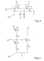
- FIG. 3 illustrates a simplified implementation of a multi-tanh doublet 10 03 .
- a so-called multi-tanh doublet is shown which comprises two emitter-coupled pairs acting in parallel.
- the (physical) sizes of transistors Q 01 and Q 04 are typically several times different from the sizes of Q 02 and Q 03 which is the other emitter-coupled pair.
- the linearity can be increased, there will be a decrease of gain in transconductance compared with an EPC and, addition thereto, the actual linearity improvement is limited due to the fundamental weakness of the emitter-coupled pair.
- the reason that the linearity is limited for emitter-coupled pairs is that the incremental tranconductance g m of the transistors in the emitter-coupled pair decreases considerably with increasing input voltage applied across the bases of the transistors.
- mixers and amplifiers based on an ECP transconductance stage are often considered insufficient as far as the fulfillment of linearity requirements are concerned for many applications.
- the micromixer A highly linear variant of the Gilbert Mixer using a bisymmetric class-AB input stage
- IEEE Journal of Solid-State Circuits, Vol. 32, no. 9, Sept. 1997, by Barrie Gilbert a solution to the problem referred to above is suggested.
- a simplified circuit diagram of the transconductance stage used in a so-called micromixer is schematically illustrated in Fig. 4 .
- the output currents I+ and I- for a given input signal Vin should be equal in amplitude and opposite in phase.
- the resistors R 01 , R 02 and R 03 are used to increase the input impedance since, the input impedance of Q 02 and Q 03 normally is quite low.
- V be (Q 02 ) + V be (Q 03 ) V b - I DC (R 03 + R 02 ) decreases, V b being the biasing voltage at the base of Q 03 . It has here been assumed that the DC currents I DC through Q 02 and Q 03 are equal and the emitter resistors of the transistors are included in R 02 and R 03 .
- a voltage-to-current transconductance stage arrangement as initially referred to which has a good or high linearity.
- a transconductance stage with a function of single-input to differential-output balun is needed which is compact and which does not consume a large chip area and still is highly linear. Even more particularly an arrangement is needed which has a high linearity without there being any losses in transconductivity.
- a transconductance stage is needed which is not limited due to for example ECP weakness as discussed above or particularly, which is such that the linearity and the transconductivity can be kept also with an increased input voltage.
- a transconductance stage is needed which tolerates high input signals (high input voltages) and which have a large dynamical range.
- transconductance stages are needed which are cheap and easy to fabricate and which are not complex.
- Most particularly transconductance stages are needed which can be used to provide amplifiers and mixers and other components with a high linearity.
- a transconductance stage is needed which can be used in components for wireless communication systems, even more particularly receivers and transmitters of a radio requiring a high linearity.
- amplifiers, mixers, particularly receivers and transmitters are needed which are highly linear.
- a voltage-to-current transconductance stage arrangement as initially referred to is provided which further comprises a common collector transistor comprising a fourth transistor connected to the base of said second transistor.
- the base of the fourth transistor is connected to the emitter of the third transistor (and the collector of the first transistor) and the emitter of the fourth transistor is connected to the base of the second transistor.
- a fifth transistor is connected to the base of said third transistor.
- the sizes of said fourth or fourth and fifth transistor(s) respectively considerably exceed(s) the sizes of said second and third transistors.
- the emitter size of said fourth or fourth and fifth transistor respectively considerably exceed the emitter size of said second and third transistors.
- the emittor sizes of the fourth or fourth and fifth transistor respectively is about, or up to, N x the emitter size of the second and/or third transistor, wherein N is approximately 10.
- the emitter size of said fourth and/or fifth transistor respectively is more than N x the emitter size of said second and/or third transistor respectively, wherein N > 10, e.g. up to about 20. (N may of course also be smaller than 10, but normally not smaller than 4-5.)
- the collector current of said fourth or fourth and fifth transistors is/are the base biasing currents of said second and third transistors respectively. Even more particularly the fourth or fourth and fifth transistors is/are biased in an "off-state", so that the collector currents are extremely small.
- the base-emitter voltage of said fourth a fourth and fifth transistors respectively is adapted to decrease rapidly, such that the corresponding DC-voltage components of the base-emitter voltages of said second and third transistors increase or do not change, hence providing a good linearity also at large RF input power.
- resistors or inductors are provided at or connected to the emitters of said first and/or second and third transistors in order to further increase the input impedance of said transistors.
- said fourth or fourth and fifth transistors is/are arranged to increase the input impedance of said first and/or second and third transistors to the desired level such that no further or no resistors are needed to increase the input impedance of said first, second and third transistors.
- a load inductor is arranged to load the collector of, particularly, the fourth transistor.
- a load inductor may also (or alternatively) be provided to load the collector of said fifth transistor, if included.
- the base-collector (BC) junction capacitor and the load inductor form a tunable series resonator.
- the input signal i.e. the input voltage
- the tunable series resonator as discussed above is adapted to be tuned such that resonance will occur at twice the input frequency, i.e. at 2 x ⁇ 0 , such that the second harmonic of the input signal will be shorted to ground at the input, in order to further increase the linearity by reducing the third order intermodulation due to the interaction between the component of 2 x ⁇ 0 and the fundamental one.
- the transistors are bipolar transistors. More particularly the transconductance stage is implemented in SiGe or GaAs. It should be clear that also other materials can be used and it does not have to be bipolar transistors but FET or CMOS etc may also be possible. Particularly the arrangement comprises an integrated circuit (IC) .
- IC integrated circuit
- a mixer comprising a transconductance stage as discussed above is also provided.
- An amplifier may also be provided comprising a transconductance stage in agreement with any one of the embodiments discussed above.
- a transconductance stage as discussed above is used in one or more components in a wireless communication system in order to provide for a high linearity for example in receivers and transmitters. Also other implementations are of course possible.
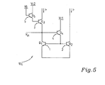
- two common collector transistors Q 4 4, Q 5 5 are provided or connected to the bases of Q 2 and Q 3 2, 3 substantially corresponding to Q 02 and Q 03 of Fig. 4 .
- transistor Q 4 4, but also transistor Q 5 5 plays a very important role in improving the linearity of the transconductance stage.
- the DC component of the base emitter voltage of Q 2 2 increases as the input power increases or keeps out of change, which is completely different from the arrangement shown in Fig. 4 .
- the transconductance stage is capable to tolerate larger input signals and its dynamic range will be extended to a large extend.
- the size of Q 4 4 and Q 5 5 respectively considerably exceeds the size of Q 2 2 and Q 3 3.
- the size here means the physical size i.e. the emitter width multiplying the length.
- the ratio of the emitter sizes may for example be as large as 10:1. It should be clear that this of course merely is one example and the ratio can be smaller as well as considerably larger as well for example down to 4:1 up to 20:1 or even more. This is to avoid that the AC voltage at input mainly is supplied to the base-emitter ports of Q 4 4 and Q 5 5. It should be noted that the AC voltage at input is split between the base-emitter port of Q 2 2 and Q 4 4, or Q 3 3 and Q 5 5.
- Q 4 4 and Q 5 5 are biased, in an off state such that their quiescent collector current will be extremely small since these currents form the base bias currents of Q 2 2 and Q 3 3.
- the base-emitter voltage of Q 4 and Q 5 will decrease rapidly as the input power increases. This in turn will produce an increase in the corresponding DC voltages of Q 2 2 and Q 3 3.
- the linearity of the transconductance stage will be improved, particularly at large RF input powers.
- the input impedance is increased by adding Q 4 4 and Q 5 5 hence reducing or even eliminating the need of resistors R 01 , R 02 , R 03 as used in the Micromixer of Fig. 4 to boost the input impedance. In the embodiment of Fig. 5 such resistors are eliminated.
- transistor Q 4 is provided as in Fig. 5 , i.e. transistor Q 5 5 is not included.
- transistor Q 5 5 is not included.
- the features correspond to the once discussed with refrence to Fig. 5 .
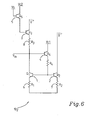
- Fig. 6 shows another embodiment, similar to Fig. 5 , with an arrangement 10 2 in which resistors R 1 , R 2 , R 3 , R 4 are provided in order to still further increase the input impedance though they need not have to be used as they do in the Micromixer shown in Fig. 4 .
- resistors R 1 , R 2 , R 3 , R 4 are provided in order to still further increase the input impedance though they need not have to be used as they do in the Micromixer shown in Fig. 4 .
- resistors R 1 -R 4 can be replaced by inductors.
- Fig. 7 shows an arrangement 10 3 in which an inductor L 1 is used as a collector load to Q 4 .
- This inductor L 1 and the base collector junction capacitance of Q 4 4 will form a series resonator that can be tuned such that the resonance occurs at 2 x ⁇ 0 , wherein ⁇ 0 denotes the frequency of the input signal. This means that the second harmonic of the input signal will be shorted to ground at the input further increasing the linearity.
- transistor Q 5 5 is shown in Fig. 7 , it should be clear that the inclusion of transistor Q 5 5 relates to a particularly advantageous embodiment, the main thing being that transistor Q 4 4 is included.
- transistors are implemented as bipolar transistors, in a most advantageous implementation.
- MOSFETs or other MOS devices or similar.
- Most appropriate seem to be SiGe HBT and GaAs HBT implementations.
Landscapes
- Engineering & Computer Science (AREA)
- Power Engineering (AREA)
- Physics & Mathematics (AREA)
- Nonlinear Science (AREA)
- Amplifiers (AREA)
- Semiconductor Lasers (AREA)
- Ultra Sonic Daignosis Equipment (AREA)
- Control Of Motors That Do Not Use Commutators (AREA)
Abstract
Description
- The present invention relates to a voltage-to-current transconductance stage arrangement comprising a single-ended input, an emitter-coupled pair of transistors comprising a first and a second transistor, whereby the emitter of a third transistor is connected to the collector of said first transistor, and a differential output. The invention also relates to a mixer and an amplifier comprising a transconductance stage arrangement.
- In many different kinds of circuits it is a requirement that the linearity is high. Examples of such arrangements or components are receivers and radio transmitters in wireless communication systems. Often the linearity of such arrangements is determined to a large extent, or mainly, by the linearity of amplifiers and mixers used in the system. Important for the linearity of such amplifiers or mixers, is the voltage-to-current transconductance stage which actually to a large extent constitutes the limiting factor as far as the linearity is concerned.
- Balanced circuits are often advantageous for several reasons compared to single-ended circuits. For example they are capable of cancelling the RF (Radio Frequency) signal at the output of a mixer used for frequency down-conversion. In order to be able to build a balanced circuit, often a single-ended input to differential output stage is needed. Such a stage can be provided in different ways. For instance, it is known to use a single-ended input to differential output passive balun (balanced-unbalanced circuit) before the transconductance stage. A passive balun consisting of inductors and capacitors however requires a large chip area and normally introduces losses, which is clearly disadvantageous.
- It is also known to use an active circuit acting as a balun and a transconductance stage simultaneously, comprising an emitter-coupled-pair (ECP). Such a single-to-differential emitter-coupled pair 1001 is shown in
Fig. 1 . A transconductance stage of this kind can be made very compact and may also provide a gain in voltage-to-current conversion. - In order to improve the linearity of the ECP transconductance stage, emitter degeneration techniques are often used. An example of such an arrangement 1002 is illustrated in
Fig. 2 wherein resistors Re1, Re2 are introduced at the emitter side of the respective transistors Q01, Q02. - Linearity can also be enhanced by implementing the multi-tanh principle as described in "The multi-tanh principle: a tutorial overview", IEEE J. Solid-State Circuits, Vol. 33, no. 1, Jan. 1998 by Barrie Gilbert. Parallel connected sets of differential pairs (EPC) of transistors are then used. Such transconductance cells or stages are known as the multi-tanh principle based cells, the main idea being that the individually non-linear (hyperbolic tangent, tanh) transconductance functions may be separated along the input-voltage axis in order to achieve a more linear overall function. The simplest one is the so-called "doublet", but other, for example the "triplet" are also known.
Fig. 3 illustrates a simplified implementation of a multi-tanh doublet 1003. InFig. 3 a so-called multi-tanh doublet is shown which comprises two emitter-coupled pairs acting in parallel. The (physical) sizes of transistors Q01 and Q04 are typically several times different from the sizes of Q02 and Q03 which is the other emitter-coupled pair. However, even if the linearity can be increased, there will be a decrease of gain in transconductance compared with an EPC and, addition thereto, the actual linearity improvement is limited due to the fundamental weakness of the emitter-coupled pair. The reason that the linearity is limited for emitter-coupled pairs is that the incremental tranconductance gm of the transistors in the emitter-coupled pair decreases considerably with increasing input voltage applied across the bases of the transistors. - Therefor mixers and amplifiers based on an ECP transconductance stage are often considered insufficient as far as the fulfillment of linearity requirements are concerned for many applications.
- In "The micromixer: A highly linear variant of the Gilbert Mixer using a bisymmetric class-AB input stage", IEEE Journal of Solid-State Circuits, Vol. 32, no. 9, Sept. 1997, by Barrie Gilbert a solution to the problem referred to above is suggested. A simplified circuit diagram of the transconductance stage used in a so-called micromixer is schematically illustrated in
Fig. 4 . The output currents I+ and I- for a given input signal Vin should be equal in amplitude and opposite in phase. The resistors R01, R02 and R03 are used to increase the input impedance since, the input impedance of Q02 and Q03 normally is quite low. However, even if the linearity can be improved as compared to ECP implementations, it is a problem with micromixer transconductances that the linearity deteriorates or goes down rapidly as the input RF power increases further. This is due to the fact that the DC component of a base-emitter voltage of Q02 and Q03, Vbe, decreases as the input RF power increases. This gives rise to gain compression and causes signal distortions. The reason for the decrease of Vbe can be explained as follow: When the input power increases, DC currents IDc through the emitters of Q02 and Q03 increase. Thus the DC voltage Vbe (Q02) + Vbe (Q03) = Vb - IDC (R03 + R02) decreases, Vb being the biasing voltage at the base of Q03. It has here been assumed that the DC currents IDC through Q02 and Q03 are equal and the emitter resistors of the transistors are included in R02 and R03. - Other related art is taught in
US5095284 ,US5182477 ,US5767662 ,US5497123 ,US4956615 ,US4049977 ,US5548248 , and in the IEEE article 'High-Frequency Nonlinearity Analysis of Common Emitter and Differential-Pair Transconductance Stages', by K. L. Fong and R. G. Meyer, Journal of Solid-state Circuits, vol. 33, no. 4, April 1998. - Hence, there are today still no transconductances with a satisfactory linearity for several important applications, for example in wireless communication systems, but also for other applications.
- What is needed is therefore a voltage-to-current transconductance stage arrangement as initially referred to which has a good or high linearity. Particularly a transconductance stage with a function of single-input to differential-output balun is needed which is compact and which does not consume a large chip area and still is highly linear. Even more particularly an arrangement is needed which has a high linearity without there being any losses in transconductivity. Particularly a transconductance stage is needed which is not limited due to for example ECP weakness as discussed above or particularly, which is such that the linearity and the transconductivity can be kept also with an increased input voltage. Particularly a transconductance stage is needed which tolerates high input signals (high input voltages) and which have a large dynamical range. Most particularly transconductance stages are needed which are cheap and easy to fabricate and which are not complex. Most particularly transconductance stages are needed which can be used to provide amplifiers and mixers and other components with a high linearity. Particularly a transconductance stage is needed which can be used in components for wireless communication systems, even more particularly receivers and transmitters of a radio requiring a high linearity. Moreover amplifiers, mixers, particularly receivers and transmitters are needed which are highly linear.
- Therefore a voltage-to-current transconductance stage arrangement as initially referred to is provided which further comprises a common collector transistor comprising a fourth transistor connected to the base of said second transistor. Particularly the base of the fourth transistor is connected to the emitter of the third transistor (and the collector of the first transistor) and the emitter of the fourth transistor is connected to the base of the second transistor. In a particularly advantageous embodiment a fifth transistor is connected to the base of said third transistor. Preferably the sizes of said fourth or fourth and fifth transistor(s) respectively considerably exceed(s) the sizes of said second and third transistors. Particularly the emitter size of said fourth or fourth and fifth transistor respectively considerably exceed the emitter size of said second and third transistors. Particularly the emittor sizes of the fourth or fourth and fifth transistor respectively is about, or up to, N x the emitter size of the second and/or third transistor, wherein N is approximately 10.
- Even more particularly the emitter size of said fourth and/or fifth transistor respectively is more than N x the emitter size of said second and/or third transistor respectively, wherein N > 10, e.g. up to about 20. (N may of course also be smaller than 10, but normally not smaller than 4-5.)
- In a particular embodiment the collector current of said fourth or fourth and fifth transistors is/are the base biasing currents of said second and third transistors respectively. Even more particularly the fourth or fourth and fifth transistors is/are biased in an "off-state", so that the collector currents are extremely small.
- Particularly, for an increasing input power, the base-emitter voltage of said fourth a fourth and fifth transistors respectively is adapted to decrease rapidly, such that the corresponding DC-voltage components of the base-emitter voltages of said second and third transistors increase or do not change, hence providing a good linearity also at large RF input power.
- In one embodiment resistors or inductors are provided at or connected to the emitters of said first and/or second and third transistors in order to further increase the input impedance of said transistors. Even more advantageously said fourth or fourth and fifth transistors is/are arranged to increase the input impedance of said first and/or second and third transistors to the desired level such that no further or no resistors are needed to increase the input impedance of said first, second and third transistors.
- In one particular implementation a load inductor is arranged to load the collector of, particularly, the fourth transistor. A load inductor may also (or alternatively) be provided to load the collector of said fifth transistor, if included.
- In one implementation the base-collector (BC) junction capacitor and the load inductor (that optionally may be provided as discussed above) form a tunable series resonator. Particularly the input signal, i.e. the input voltage, has a frequency w0 and the tunable series resonator as discussed above is adapted to be tuned such that resonance will occur at twice the input frequency, i.e. at 2 x ω0, such that the second harmonic of the input signal will be shorted to ground at the input, in order to further increase the linearity by reducing the third order intermodulation due to the interaction between the component of 2 x ω0 and the fundamental one.
- In particular implementations the transistors are bipolar transistors. More particularly the transconductance stage is implemented in SiGe or GaAs. It should be clear that also other materials can be used and it does not have to be bipolar transistors but FET or CMOS etc may also be possible. Particularly the arrangement comprises an integrated circuit (IC) .
- Therefore, in order to solve the problems referred to earlier, a mixer comprising a transconductance stage as discussed above is also provided. An amplifier may also be provided comprising a transconductance stage in agreement with any one of the embodiments discussed above. Most particularly a transconductance stage as discussed above is used in one or more components in a wireless communication system in order to provide for a high linearity for example in receivers and transmitters. Also other implementations are of course possible.
- The invention will in the following be further described, in a non-limiting manner, and with reference with the accompanying drawings, in which:
- Fig. 1
- shows a known active circuit acting as a single-to- diffenerential balun and transconductance stage at the same time and comprising an emitter-coupled pair,
- Fig. 2
- shows an ECP transconductance stage as in
Fig. 1 but with resistors for emitter degeneration, - Fig. 3
- shows another known transconductance stage comprising ECPs, the so-called multi-tahn doublet,
- Fig. 4
- shows the known transconductance stage used in a Micromixer,
- Fig. 5
- shows a transconductance stage according to a first embodiment of the present invention,
- Fig. 6
- shows a slightly modified embodiment of the transconductance stage of
Fig. 5 , and - Fig. 7
- shows another embodiment of the present invention with a collector loading inductor.
-
-
Fig. 1 very schematically illustrates an emitter-coupled pair (ECP) arrangement 1001 for an active circuit acting as a balun and a transconductance stage simultaneously with two emitter-coupled transistors Q01, Q02. -
Fig. 2 schematically illustrates a similar ECP transconductance stage 1002 but with resistors Re1, Re2 connected to the respective emitters for emitter degeneration purposes, which is a known measure to increase the linearity of an arrangement as inFig. 1 . -
Fig. 3 shows a known multi-tanh doublet 1003. It also discloses another method for improving linearity. The sizes of Q01 and Q04 typically differ several times from the sizes of Q02 and Q03. However, all the emitter-coupled pairs are not satisfactory as far as linearity requirements are concerned for various applications, particularly due to the transconductance of the transistors decreasing considerably with an increasing input voltage applied across the bases of the transistors. -
Fig. 4 schematically shows a known so called micromixer 1004 according to one implementation, or more specifically the transconductance stage used in a micromixer. The output currents I+ and I- for a given input signal Vin are equal in amplitude and opposite in phase. The resistors R01, R02, R03, as also discussed above, are used to increase the input impedance. The linearity, however, goes down rapidly as the input RF power increases due to the fact that the DC component of the base emitter voltage of Q02 and Q03, i.e. VBE decreases with an increasing input power. As discussed above when the input power increases, the DC currents through the emitters of Q02 and Q03 increase and the DC voltage VBE (Q02) + VBE (Q03) = Vb - IDC (R03 + R02) decreases, Vb being the biasing voltage at the Q03 base. -
Fig. 5 shows an arrangement according to the present invention wherein the problems with among others decreased linearity or deteriorated linearity at increasing input of power are reduced or overcome. InFig. 5 a single ended input-to differential output transconductance stage 101 is illustrated. - According to this embodiment of the invention two common
collector transistors Q 4 4,Q 5 5 are provided or connected to the bases of Q2 andQ Fig. 4 . Particularlytransistor Q 4 4, but alsotransistor Q 5 5 plays a very important role in improving the linearity of the transconductance stage. Actually, instead of decreasing, the DC component of the base emitter voltage of Q2 2 (Vbe) increases as the input power increases or keeps out of change, which is completely different from the arrangement shown inFig. 4 . As a result thereof, the transconductance stage is capable to tolerate larger input signals and its dynamic range will be extended to a large extend. - According to the invention the size of
Q 4 4 andQ 5 5 respectively considerably exceeds the size ofQ 2 2 andQ 3 3. The size here means the physical size i.e. the emitter width multiplying the length. The ratio of the emitter sizes may for example be as large as 10:1. It should be clear that this of course merely is one example and the ratio can be smaller as well as considerably larger as well for example down to 4:1 up to 20:1 or even more. This is to avoid that the AC voltage at input mainly is supplied to the base-emitter ports ofQ 4 4 andQ 5 5. It should be noted that the AC voltage at input is split between the base-emitter port ofQ 2 2 andQ 4 4, orQ 3 3 andQ 5 5. -
Advantageously Q 4 4 andQ 5 5 are biased, in an off state such that their quiescent collector current will be extremely small since these currents form the base bias currents ofQ 2 2 andQ 3 3. According to the invention the base-emitter voltage of Q4 and Q5 will decrease rapidly as the input power increases. This in turn will produce an increase in the corresponding DC voltages ofQ 2 2 andQ 3 3. Hence, with a circuit configuration according to the present invention, the linearity of the transconductance stage will be improved, particularly at large RF input powers. Moreover, the input impedance is increased by addingQ 4 4 andQ 5 5 hence reducing or even eliminating the need of resistors R01, R02, R03 as used in the Micromixer ofFig. 4 to boost the input impedance. In the embodiment ofFig. 5 such resistors are eliminated. - In another embodiment (not shown) only
transistor Q 4 is provided as inFig. 5 , i.e.transistor Q 5 5 is not included. In every other aspect of such an embodiment, the features correspond to the once discussed with refrence toFig. 5 . -
Fig. 6 shows another embodiment, similar toFig. 5 , with an arrangement 102 in which resistors R1, R2, R3, R4 are provided in order to still further increase the input impedance though they need not have to be used as they do in the Micromixer shown inFig. 4 . This also applies to an embodiment as discussed above in which onlytransistor Q 4 4 is provided. It should be noted that all or same of the resistors R1-R4 can be replaced by inductors. -
Fig. 7 shows an arrangement 103 in which an inductor L1 is used as a collector load to Q4. This inductor L1 and the base collector junction capacitance ofQ 4 4 will form a series resonator that can be tuned such that the resonance occurs at 2 x ω0, wherein ω0 denotes the frequency of the input signal. This means that the second harmonic of the input signal will be shorted to ground at the input further increasing the linearity. Althoughtransistor Q 5 5 is shown inFig. 7 , it should be clear that the inclusion oftransistor Q 5 5 relates to a particularly advantageous embodiment, the main thing being thattransistor Q 4 4 is included. - Particularly the transistors are implemented as bipolar transistors, in a most advantageous implementation. In an alternative implementation they are implemented as MOSFETs, or other MOS devices or similar. Most appropriate seem to be SiGe HBT and GaAs HBT implementations.
- The implementation of an arrangement in IC design is straightforward and does not require any unusual measure or procedures. From the IC design point of view, the addition of transistor Q4 or the two transistors, Q4, Q5 and possible one or more inductors e.g. in order to load Q4 and/or Q5, will not add to the complexity of the circuit or affect it in any substantial way, except for improving linearity. The noise figure might increase slightly.
- It should be clear that although a part of the circuit consisting of transistors Q1, Q2 is in a form similar to a current mirror with a so called β helper Q4, it should also be clear that they play fundamentally different roles and Q4 according to present invention is an integrated part of the active transconductance stage. The input RF signal applies to Q4. In contrast, in the current mirror construction the corresponding counterpart to Q4 serves the purpose of DC biasing in order to stabilize the mirror current and it is entirely isolated from the input RF signal.
- It should be clear that the invention can be varied in a number of ways within the scope of the appended claims and it is in no way limited to the explicitly discussed and illustrated embodiments but different materials and different sizes can be used and additional loads such as inductors and resistors etc can be added in order to provide for specific properties although they are not necessary for the concept of the invention.
Claims (22)
- A voltage-to-current transconductance stage arrangement comprising a single-ended input, an emitter-coupled pair of transistors (1,2), comprising a first transistor (1) and a second transistor (2), the emitter of a third transistor (3), being connected to the collector of said first transistor (1), and a differential output,
characterized in
that it further comprises a common-collector transistor comprising a fourth transistor (4) connected to the base of said second transistor (2) and in that the size of said fourth (4) considerably exceeds the sizes of said second and third transistors. - A transconductance stage arrangement according to claim 1, characterized in
the the fourth transistor (4) further is connected to the emitter of the third transistor (3) and preferably to the collector of the first transistor (1). - A transconductance stage arrangement according to claim 1 or 2,
characterized in
that a fifth transistor (5) connected to the base of said third transistor (3). - A transconductance stage arrangement according to any one of claims 1-3,
characterized in
that the emitter size of said fourth (4) or fourth and fifth (5) transistor respectively considerably exceeds the emitter size of said second and third transistors (2,3). - A transconductance stage arrangement according to claim 4, characterized in
that the emitter size of said fourth or fourth and fifth transistor (4,5) respectively is about, or up to, N x the emitter size of the second and/or third transistor (2,3), N ≈ 10. - A transconductance stage arrangement according to claim 4, characterized in
that the emitter size of said fourth (4) or fourth and fifth transistor (4,5) respectively is more than N x the emitter size of said second and/or third transistor (2,3) respectively, N > 10. - A transconductance stage arrangement according to any one of claims 1-6,
characterized in
that the collector currents of said fourth (4) or fourth and fifth transistors (4,5) are the base biasing currents of said second and third transistors (2,3) respectively. - A transconductance stage arrangement according to claim 7, characterized in
that the collector currents of said fourth (4) or fourth and fifth transistors (4,5) are adapted to be biased in an off-state of the respective transistor in such way that they are extremely small. - A transconductance stage arrangement according to claim 6 or 7,
characterized in
that second biasing means (5) are provided for biasing the collector currents of said fourth (4) and/or fifth transistors (4,5) in such a manner that said collector currents forming the base biasing currents of said second and third transistors get extremely small. - A transconductance stage arrangement according to any one of the preceding claims,
characterized in
that for an increasing input power, the base-emitter voltage of said fourth (4) or fourth and fifth transistors (4,5) respectively is adapted to decrease rapidly such that the corresponding DC-voltage components of the base-emitter voltages of said second and third transistors (2,3) increase, hence providing a good linearity also at large RF input power. - A transconductance stage arrangement according to any one of the preceding claims,
characterized in
that said fourth (4) or fourth and fifth transistors (4,5) is/are arranged to increase the input impedance of said first and/or second and/or third transistors (1,2,3) to a desired level. - A transconductance stage arrangement according to claim 11, characterized in
that resistors (6,7,8) or inductors are provided at or connected to the emitters of said first and/or second and/or third transistors (1,2,3) in order to further increase the input impedance of said transistors. - A transconductance stage arrangement according to any one of the preceding claims,
characterized in
that a load inductor (5) is arranged to load the collector of the fourth transistor (4). - A transconductance stage arrangement according to claim 12, characterized in
that the fourth transistor (4) comprises a base-collector junction capacitor and in that said capacitor and the load inductor (4) form a tunable series resonator. - A transconductance stage arrangement according to claim 14, characterized in
that the input signal has a frequency ω0, and in that the tunable series resonator is adapted to be tuned such that resonance will occur at twice the input frequency, i.e. at 2ω0 such that the second harmonic of the input signal will be shorted to ground at input. - A transconductance stage arrangement according to any one of the preceding claims,
characterized in
that the transistors (1,2,3,4,5) are bipolar transistors. - A transconductance stage arrangement according to any one of the preceding claims,
characterized in
that it is implemented in SiGe or GaAS. - A transconductance stage arrangement according to any one of the preceding claims,
characterized in
that it comprises an integrated circuit (IC). - A transconductance stage arrangement according to any one of claims 1-18,
characterized in
that said fourth transistor or said fourth and fifth transistors (4,5) is/are in off-state. - A mixer comprising a transconductance stage arrangement according to any one of claims 1-19.
- An amplifier comprising a transconductance stage arrangement according to any one of claims 1-19.
- Use of a transconductance stage arrangement according to any one of claims 1-17 in a component in a wireless communication system.
Applications Claiming Priority (1)
| Application Number | Priority Date | Filing Date | Title |
|---|---|---|---|
| PCT/SE2005/001564 WO2007046732A1 (en) | 2005-10-20 | 2005-10-20 | A transconductance stage arrangement |
Publications (2)
| Publication Number | Publication Date |
|---|---|
| EP1946440A1 EP1946440A1 (en) | 2008-07-23 |
| EP1946440B1 true EP1946440B1 (en) | 2011-04-20 |
Family
ID=37962745
Family Applications (1)
| Application Number | Title | Priority Date | Filing Date |
|---|---|---|---|
| EP05794514A Expired - Lifetime EP1946440B1 (en) | 2005-10-20 | 2005-10-20 | A transconductance stage arrangement |
Country Status (7)
| Country | Link |
|---|---|
| US (1) | US7626461B2 (en) |
| EP (1) | EP1946440B1 (en) |
| JP (1) | JP5065280B2 (en) |
| CN (1) | CN101297477B (en) |
| AT (1) | ATE506745T1 (en) |
| DE (1) | DE602005027624D1 (en) |
| WO (1) | WO2007046732A1 (en) |
Families Citing this family (6)
| Publication number | Priority date | Publication date | Assignee | Title |
|---|---|---|---|---|
| EP1997223A1 (en) * | 2006-03-09 | 2008-12-03 | Nxp B.V. | Amplification stage |
| US7894780B2 (en) * | 2006-12-06 | 2011-02-22 | Broadcom Corporation | Method and system for a linearized transmitter including a power amplifier |
| JP2009201048A (en) * | 2008-02-25 | 2009-09-03 | Nippon Telegr & Teleph Corp <Ntt> | Flip-flop circuit and semiconductor device |
| US8306494B2 (en) * | 2008-08-14 | 2012-11-06 | Broadcom Corporation | Method and system for a single-ended input low noise amplifier with differential output |
| CN102638227A (en) * | 2012-04-23 | 2012-08-15 | 中国科学院微电子研究所 | Ultra-wideband mixer circuit with on-chip active balun |
| CN103580619B (en) * | 2012-08-08 | 2018-03-23 | 中兴通讯股份有限公司 | A kind of power amplifier device and linear regulator |
Family Cites Families (23)
| Publication number | Priority date | Publication date | Assignee | Title |
|---|---|---|---|---|
| JPS5862908A (en) * | 1981-10-08 | 1983-04-14 | Nippon Telegr & Teleph Corp <Ntt> | Voltage current converting circuit |
| JPS59181807A (en) * | 1983-03-31 | 1984-10-16 | Toshiba Corp | Transistor amplifier |
| JPS59221014A (en) * | 1983-05-30 | 1984-12-12 | Sony Corp | Voltage/current converting circuit |
| US4574233A (en) * | 1984-03-30 | 1986-03-04 | Tektronix, Inc. | High impedance current source |
| JPS61164309A (en) * | 1985-01-17 | 1986-07-25 | Matsushita Electric Ind Co Ltd | signal conversion circuit |
| JPH0636484B2 (en) * | 1988-09-08 | 1994-05-11 | 日本電気株式会社 | Current-voltage conversion circuit |
| US5182477A (en) * | 1990-03-22 | 1993-01-26 | Silicon Systems, Inc. | Bipolar tunable transconductance element |
| US5095284A (en) * | 1990-09-10 | 1992-03-10 | Synaptics, Incorporated | Subthreshold CMOS amplifier with wide input voltage range |
| JP3153569B2 (en) * | 1991-04-15 | 2001-04-09 | パイオニア株式会社 | Voltage-current converter |
| JPH0514072A (en) * | 1991-07-08 | 1993-01-22 | Fujitsu Ltd | Semiconductor device |
| US5497123A (en) * | 1994-12-23 | 1996-03-05 | Motorola, Inc. | Amplifier circuit having high linearity for cancelling third order harmonic distortion |
| JP2669389B2 (en) * | 1995-03-24 | 1997-10-27 | 日本電気株式会社 | Voltage-current converter |
| CN1155183A (en) * | 1995-11-28 | 1997-07-23 | 汤姆森消费电子有限公司 | Low-power transconductance drive amplifier |
| GB2321149B (en) * | 1997-01-11 | 2001-04-04 | Plessey Semiconductors Ltd | Low voltage double balanced mixer |
| JPH10247846A (en) * | 1997-03-04 | 1998-09-14 | Sony Corp | Input circuit |
| US5929710A (en) * | 1997-03-20 | 1999-07-27 | National Semiconductor Corporation | Cascode single-ended to differential converter |
| US5999804A (en) * | 1997-03-20 | 1999-12-07 | National Semiconductor Corporation | Low noise quadrature mixer circuit |
| SE515138C2 (en) * | 1999-10-29 | 2001-06-18 | Ericsson Telefon Ab L M | transconductor |
| JP2002305429A (en) * | 2001-04-05 | 2002-10-18 | Fujitsu Ltd | Conversion circuit |
| JP2002368547A (en) * | 2001-06-11 | 2002-12-20 | Hitachi Kokusai Electric Inc | Distortion improvement circuit |
| US6819184B2 (en) * | 2002-11-06 | 2004-11-16 | Cree Microwave, Inc. | RF transistor amplifier linearity using suppressed third order transconductance |
| JP2005176331A (en) * | 2003-11-21 | 2005-06-30 | Matsushita Electric Ind Co Ltd | Amplifier and transmitter and communication device using the same |
| US7671686B2 (en) * | 2007-10-24 | 2010-03-02 | Industrial Technology Research Institute | Low noise amplifier |
-
2005
- 2005-10-20 AT AT05794514T patent/ATE506745T1/en not_active IP Right Cessation
- 2005-10-20 WO PCT/SE2005/001564 patent/WO2007046732A1/en not_active Ceased
- 2005-10-20 DE DE602005027624T patent/DE602005027624D1/en not_active Expired - Lifetime
- 2005-10-20 JP JP2008536537A patent/JP5065280B2/en not_active Expired - Fee Related
- 2005-10-20 US US12/090,710 patent/US7626461B2/en not_active Expired - Fee Related
- 2005-10-20 EP EP05794514A patent/EP1946440B1/en not_active Expired - Lifetime
- 2005-10-20 CN CN2005800518861A patent/CN101297477B/en not_active Expired - Fee Related
Also Published As
| Publication number | Publication date |
|---|---|
| CN101297477A (en) | 2008-10-29 |
| DE602005027624D1 (en) | 2011-06-01 |
| CN101297477B (en) | 2011-02-02 |
| EP1946440A1 (en) | 2008-07-23 |
| JP2009513059A (en) | 2009-03-26 |
| ATE506745T1 (en) | 2011-05-15 |
| US20080265992A1 (en) | 2008-10-30 |
| US7626461B2 (en) | 2009-12-01 |
| WO2007046732A1 (en) | 2007-04-26 |
| JP5065280B2 (en) | 2012-10-31 |
Similar Documents
| Publication | Publication Date | Title |
|---|---|---|
| US6229395B1 (en) | Differential transconductance amplifier | |
| US8554162B2 (en) | High efficiency power amplifier | |
| US8279003B2 (en) | Differential RF amplifier | |
| US8577322B1 (en) | Signal mixer having a single-ended input and a differential output | |
| US7602227B2 (en) | Differential amplifier circuit and mixer circuit having improved linearity | |
| KR100867549B1 (en) | Resonant Active Balun | |
| US10014835B1 (en) | Frequency enhanced active transistor | |
| US7626461B2 (en) | Transconductance stage arrangement | |
| EP1039629B1 (en) | An amplifier circuit arrangement | |
| US7242236B2 (en) | Mixer circuit with phase-shifted radio frequency signal | |
| JP4567831B2 (en) | Voltage-current converter | |
| US6538501B2 (en) | Radio frequency amplifier and tuner | |
| US6535062B1 (en) | Low noise, low distortion, complementary IF amplifier | |
| KR100351419B1 (en) | A low-voltage balun circuit | |
| US7342432B2 (en) | Mixer circuit having improved linearity and noise figure | |
| US7345548B2 (en) | Radiofrequency amplifier device, in particular for cellular mobile telephone | |
| Bowers et al. | Recent developments in bipolar operational amplifiers | |
| US20250096749A1 (en) | Power amplifier circuit | |
| KR20080059231A (en) | Interconducting end device | |
| JP2004357091A (en) | Mixer circuit | |
| Centurelli et al. | A novel dual-output CCII-based single-ended to differential converter | |
| WO2026014313A1 (en) | Bias circuit and amplifier | |
| US20090295454A1 (en) | Low voltage mixer circuit | |
| CN119318112A (en) | Circuit for connecting the two outputs of a differential amplifier to the input of a single-ended amplifier | |
| KR20100027758A (en) | Mixer using current mirroring |
Legal Events
| Date | Code | Title | Description |
|---|---|---|---|
| PUAI | Public reference made under article 153(3) epc to a published international application that has entered the european phase |
Free format text: ORIGINAL CODE: 0009012 |
|
| 17P | Request for examination filed |
Effective date: 20080430 |
|
| AK | Designated contracting states |
Kind code of ref document: A1 Designated state(s): AT BE BG CH CY CZ DE DK EE ES FI FR GB GR HU IE IS IT LI LT LU LV MC NL PL PT RO SE SI SK TR |
|
| GRAP | Despatch of communication of intention to grant a patent |
Free format text: ORIGINAL CODE: EPIDOSNIGR1 |
|
| DAX | Request for extension of the european patent (deleted) | ||
| GRAS | Grant fee paid |
Free format text: ORIGINAL CODE: EPIDOSNIGR3 |
|
| GRAA | (expected) grant |
Free format text: ORIGINAL CODE: 0009210 |
|
| AK | Designated contracting states |
Kind code of ref document: B1 Designated state(s): AT BE BG CH CY CZ DE DK EE ES FI FR GB GR HU IE IS IT LI LT LU LV MC NL PL PT RO SE SI SK TR |
|
| REG | Reference to a national code |
Ref country code: GB Ref legal event code: FG4D |
|
| REG | Reference to a national code |
Ref country code: CH Ref legal event code: EP |
|
| REG | Reference to a national code |
Ref country code: IE Ref legal event code: FG4D |
|
| REF | Corresponds to: |
Ref document number: 602005027624 Country of ref document: DE Date of ref document: 20110601 Kind code of ref document: P |
|
| REG | Reference to a national code |
Ref country code: DE Ref legal event code: R096 Ref document number: 602005027624 Country of ref document: DE Effective date: 20110601 |
|
| REG | Reference to a national code |
Ref country code: NL Ref legal event code: T3 |
|
| LTIE | Lt: invalidation of european patent or patent extension |
Effective date: 20110420 |
|
| PG25 | Lapsed in a contracting state [announced via postgrant information from national office to epo] |
Ref country code: PT Free format text: LAPSE BECAUSE OF FAILURE TO SUBMIT A TRANSLATION OF THE DESCRIPTION OR TO PAY THE FEE WITHIN THE PRESCRIBED TIME-LIMIT Effective date: 20110822 Ref country code: LT Free format text: LAPSE BECAUSE OF FAILURE TO SUBMIT A TRANSLATION OF THE DESCRIPTION OR TO PAY THE FEE WITHIN THE PRESCRIBED TIME-LIMIT Effective date: 20110420 Ref country code: SE Free format text: LAPSE BECAUSE OF FAILURE TO SUBMIT A TRANSLATION OF THE DESCRIPTION OR TO PAY THE FEE WITHIN THE PRESCRIBED TIME-LIMIT Effective date: 20110420 |
|
| PG25 | Lapsed in a contracting state [announced via postgrant information from national office to epo] |
Ref country code: SI Free format text: LAPSE BECAUSE OF FAILURE TO SUBMIT A TRANSLATION OF THE DESCRIPTION OR TO PAY THE FEE WITHIN THE PRESCRIBED TIME-LIMIT Effective date: 20110420 Ref country code: BE Free format text: LAPSE BECAUSE OF FAILURE TO SUBMIT A TRANSLATION OF THE DESCRIPTION OR TO PAY THE FEE WITHIN THE PRESCRIBED TIME-LIMIT Effective date: 20110420 Ref country code: ES Free format text: LAPSE BECAUSE OF FAILURE TO SUBMIT A TRANSLATION OF THE DESCRIPTION OR TO PAY THE FEE WITHIN THE PRESCRIBED TIME-LIMIT Effective date: 20110731 Ref country code: LV Free format text: LAPSE BECAUSE OF FAILURE TO SUBMIT A TRANSLATION OF THE DESCRIPTION OR TO PAY THE FEE WITHIN THE PRESCRIBED TIME-LIMIT Effective date: 20110420 Ref country code: GR Free format text: LAPSE BECAUSE OF FAILURE TO SUBMIT A TRANSLATION OF THE DESCRIPTION OR TO PAY THE FEE WITHIN THE PRESCRIBED TIME-LIMIT Effective date: 20110721 Ref country code: AT Free format text: LAPSE BECAUSE OF FAILURE TO SUBMIT A TRANSLATION OF THE DESCRIPTION OR TO PAY THE FEE WITHIN THE PRESCRIBED TIME-LIMIT Effective date: 20110420 Ref country code: FI Free format text: LAPSE BECAUSE OF FAILURE TO SUBMIT A TRANSLATION OF THE DESCRIPTION OR TO PAY THE FEE WITHIN THE PRESCRIBED TIME-LIMIT Effective date: 20110420 Ref country code: CY Free format text: LAPSE BECAUSE OF FAILURE TO SUBMIT A TRANSLATION OF THE DESCRIPTION OR TO PAY THE FEE WITHIN THE PRESCRIBED TIME-LIMIT Effective date: 20110420 Ref country code: IS Free format text: LAPSE BECAUSE OF FAILURE TO SUBMIT A TRANSLATION OF THE DESCRIPTION OR TO PAY THE FEE WITHIN THE PRESCRIBED TIME-LIMIT Effective date: 20110820 |
|
| PG25 | Lapsed in a contracting state [announced via postgrant information from national office to epo] |
Ref country code: CZ Free format text: LAPSE BECAUSE OF FAILURE TO SUBMIT A TRANSLATION OF THE DESCRIPTION OR TO PAY THE FEE WITHIN THE PRESCRIBED TIME-LIMIT Effective date: 20110420 Ref country code: EE Free format text: LAPSE BECAUSE OF FAILURE TO SUBMIT A TRANSLATION OF THE DESCRIPTION OR TO PAY THE FEE WITHIN THE PRESCRIBED TIME-LIMIT Effective date: 20110420 |
|
| PLBE | No opposition filed within time limit |
Free format text: ORIGINAL CODE: 0009261 |
|
| STAA | Information on the status of an ep patent application or granted ep patent |
Free format text: STATUS: NO OPPOSITION FILED WITHIN TIME LIMIT |
|
| PG25 | Lapsed in a contracting state [announced via postgrant information from national office to epo] |
Ref country code: SK Free format text: LAPSE BECAUSE OF FAILURE TO SUBMIT A TRANSLATION OF THE DESCRIPTION OR TO PAY THE FEE WITHIN THE PRESCRIBED TIME-LIMIT Effective date: 20110420 Ref country code: RO Free format text: LAPSE BECAUSE OF FAILURE TO SUBMIT A TRANSLATION OF THE DESCRIPTION OR TO PAY THE FEE WITHIN THE PRESCRIBED TIME-LIMIT Effective date: 20110420 Ref country code: DK Free format text: LAPSE BECAUSE OF FAILURE TO SUBMIT A TRANSLATION OF THE DESCRIPTION OR TO PAY THE FEE WITHIN THE PRESCRIBED TIME-LIMIT Effective date: 20110420 Ref country code: PL Free format text: LAPSE BECAUSE OF FAILURE TO SUBMIT A TRANSLATION OF THE DESCRIPTION OR TO PAY THE FEE WITHIN THE PRESCRIBED TIME-LIMIT Effective date: 20110420 |
|
| 26N | No opposition filed |
Effective date: 20120123 |
|
| REG | Reference to a national code |
Ref country code: DE Ref legal event code: R097 Ref document number: 602005027624 Country of ref document: DE Effective date: 20120123 |
|
| PG25 | Lapsed in a contracting state [announced via postgrant information from national office to epo] |
Ref country code: IT Free format text: LAPSE BECAUSE OF FAILURE TO SUBMIT A TRANSLATION OF THE DESCRIPTION OR TO PAY THE FEE WITHIN THE PRESCRIBED TIME-LIMIT Effective date: 20110420 Ref country code: MC Free format text: LAPSE BECAUSE OF NON-PAYMENT OF DUE FEES Effective date: 20111031 |
|
| REG | Reference to a national code |
Ref country code: CH Ref legal event code: PL |
|
| REG | Reference to a national code |
Ref country code: FR Ref legal event code: ST Effective date: 20120629 |
|
| PG25 | Lapsed in a contracting state [announced via postgrant information from national office to epo] |
Ref country code: CH Free format text: LAPSE BECAUSE OF NON-PAYMENT OF DUE FEES Effective date: 20111031 Ref country code: LI Free format text: LAPSE BECAUSE OF NON-PAYMENT OF DUE FEES Effective date: 20111031 |
|
| REG | Reference to a national code |
Ref country code: IE Ref legal event code: MM4A |
|
| PG25 | Lapsed in a contracting state [announced via postgrant information from national office to epo] |
Ref country code: FR Free format text: LAPSE BECAUSE OF NON-PAYMENT OF DUE FEES Effective date: 20111102 |
|
| PG25 | Lapsed in a contracting state [announced via postgrant information from national office to epo] |
Ref country code: IE Free format text: LAPSE BECAUSE OF NON-PAYMENT OF DUE FEES Effective date: 20111020 |
|
| PG25 | Lapsed in a contracting state [announced via postgrant information from national office to epo] |
Ref country code: LU Free format text: LAPSE BECAUSE OF NON-PAYMENT OF DUE FEES Effective date: 20111020 |
|
| PG25 | Lapsed in a contracting state [announced via postgrant information from national office to epo] |
Ref country code: BG Free format text: LAPSE BECAUSE OF FAILURE TO SUBMIT A TRANSLATION OF THE DESCRIPTION OR TO PAY THE FEE WITHIN THE PRESCRIBED TIME-LIMIT Effective date: 20110720 |
|
| PG25 | Lapsed in a contracting state [announced via postgrant information from national office to epo] |
Ref country code: TR Free format text: LAPSE BECAUSE OF FAILURE TO SUBMIT A TRANSLATION OF THE DESCRIPTION OR TO PAY THE FEE WITHIN THE PRESCRIBED TIME-LIMIT Effective date: 20110420 |
|
| PG25 | Lapsed in a contracting state [announced via postgrant information from national office to epo] |
Ref country code: HU Free format text: LAPSE BECAUSE OF FAILURE TO SUBMIT A TRANSLATION OF THE DESCRIPTION OR TO PAY THE FEE WITHIN THE PRESCRIBED TIME-LIMIT Effective date: 20110420 |
|
| REG | Reference to a national code |
Ref country code: DE Ref legal event code: R082 Ref document number: 602005027624 Country of ref document: DE Representative=s name: GRUENECKER, KINKELDEY, STOCKMAIR & SCHWANHAEUS, DE |
|
| REG | Reference to a national code |
Ref country code: DE Ref legal event code: R082 Ref document number: 602005027624 Country of ref document: DE Representative=s name: GRUENECKER, KINKELDEY, STOCKMAIR & SCHWANHAEUS, DE Effective date: 20150119 Ref country code: DE Ref legal event code: R081 Ref document number: 602005027624 Country of ref document: DE Owner name: OPTIS CELLULAR TECHNOLOGY, LLC (N. D. GES. D. , US Free format text: FORMER OWNER: TELEFONAKTIEBOLAGET LM ERICSSON (PUBL), STOCKHOLM, SE Effective date: 20150119 Ref country code: DE Ref legal event code: R082 Ref document number: 602005027624 Country of ref document: DE Representative=s name: GRUENECKER PATENT- UND RECHTSANWAELTE PARTG MB, DE Effective date: 20150119 |
|
| REG | Reference to a national code |
Ref country code: NL Ref legal event code: SD Effective date: 20150630 |
|
| PGFP | Annual fee paid to national office [announced via postgrant information from national office to epo] |
Ref country code: GB Payment date: 20160928 Year of fee payment: 12 Ref country code: NL Payment date: 20160923 Year of fee payment: 12 |
|
| REG | Reference to a national code |
Ref country code: GB Ref legal event code: 732E Free format text: REGISTERED BETWEEN 20161020 AND 20161026 |
|
| PGFP | Annual fee paid to national office [announced via postgrant information from national office to epo] |
Ref country code: DE Payment date: 20160922 Year of fee payment: 12 |
|
| REG | Reference to a national code |
Ref country code: DE Ref legal event code: R119 Ref document number: 602005027624 Country of ref document: DE |
|
| REG | Reference to a national code |
Ref country code: NL Ref legal event code: MM Effective date: 20171101 |
|
| GBPC | Gb: european patent ceased through non-payment of renewal fee |
Effective date: 20171020 |
|
| PG25 | Lapsed in a contracting state [announced via postgrant information from national office to epo] |
Ref country code: DE Free format text: LAPSE BECAUSE OF NON-PAYMENT OF DUE FEES Effective date: 20180501 Ref country code: GB Free format text: LAPSE BECAUSE OF NON-PAYMENT OF DUE FEES Effective date: 20171020 Ref country code: NL Free format text: LAPSE BECAUSE OF NON-PAYMENT OF DUE FEES Effective date: 20171101 |