EP1944647A1 - Liquid crystal display apparatus and lighting unit - Google Patents
Liquid crystal display apparatus and lighting unit Download PDFInfo
- Publication number
- EP1944647A1 EP1944647A1 EP08000177A EP08000177A EP1944647A1 EP 1944647 A1 EP1944647 A1 EP 1944647A1 EP 08000177 A EP08000177 A EP 08000177A EP 08000177 A EP08000177 A EP 08000177A EP 1944647 A1 EP1944647 A1 EP 1944647A1
- Authority
- EP
- European Patent Office
- Prior art keywords
- cold cathode
- inverter substrate
- reflector panel
- terminals
- inverter
- Prior art date
- Legal status (The legal status is an assumption and is not a legal conclusion. Google has not performed a legal analysis and makes no representation as to the accuracy of the status listed.)
- Granted
Links
- 239000004973 liquid crystal related substance Substances 0.000 title claims description 13
- 239000000758 substrate Substances 0.000 claims abstract description 102
- 229910000679 solder Inorganic materials 0.000 claims abstract description 20
- 238000004804 winding Methods 0.000 claims description 13
- 230000005611 electricity Effects 0.000 claims description 9
- 238000012986 modification Methods 0.000 description 6
- 230000004048 modification Effects 0.000 description 6
- 238000005476 soldering Methods 0.000 description 4
- RYGMFSIKBFXOCR-UHFFFAOYSA-N Copper Chemical compound [Cu] RYGMFSIKBFXOCR-UHFFFAOYSA-N 0.000 description 3
- 229910052802 copper Inorganic materials 0.000 description 3
- 239000010949 copper Substances 0.000 description 3
- 238000009792 diffusion process Methods 0.000 description 3
- 238000005516 engineering process Methods 0.000 description 1
- 238000003780 insertion Methods 0.000 description 1
- 230000037431 insertion Effects 0.000 description 1
- 238000000034 method Methods 0.000 description 1
- 230000010355 oscillation Effects 0.000 description 1
- 230000000149 penetrating effect Effects 0.000 description 1
Images



Classifications
-
- G—PHYSICS
- G02—OPTICS
- G02F—OPTICAL DEVICES OR ARRANGEMENTS FOR THE CONTROL OF LIGHT BY MODIFICATION OF THE OPTICAL PROPERTIES OF THE MEDIA OF THE ELEMENTS INVOLVED THEREIN; NON-LINEAR OPTICS; FREQUENCY-CHANGING OF LIGHT; OPTICAL LOGIC ELEMENTS; OPTICAL ANALOGUE/DIGITAL CONVERTERS
- G02F1/00—Devices or arrangements for the control of the intensity, colour, phase, polarisation or direction of light arriving from an independent light source, e.g. switching, gating or modulating; Non-linear optics
- G02F1/01—Devices or arrangements for the control of the intensity, colour, phase, polarisation or direction of light arriving from an independent light source, e.g. switching, gating or modulating; Non-linear optics for the control of the intensity, phase, polarisation or colour
- G02F1/13—Devices or arrangements for the control of the intensity, colour, phase, polarisation or direction of light arriving from an independent light source, e.g. switching, gating or modulating; Non-linear optics for the control of the intensity, phase, polarisation or colour based on liquid crystals, e.g. single liquid crystal display cells
- G02F1/133—Constructional arrangements; Operation of liquid crystal cells; Circuit arrangements
- G02F1/1333—Constructional arrangements; Manufacturing methods
- G02F1/1335—Structural association of cells with optical devices, e.g. polarisers or reflectors
- G02F1/1336—Illuminating devices
- G02F1/133602—Direct backlight
- G02F1/133604—Direct backlight with lamps
-
- G—PHYSICS
- G02—OPTICS
- G02F—OPTICAL DEVICES OR ARRANGEMENTS FOR THE CONTROL OF LIGHT BY MODIFICATION OF THE OPTICAL PROPERTIES OF THE MEDIA OF THE ELEMENTS INVOLVED THEREIN; NON-LINEAR OPTICS; FREQUENCY-CHANGING OF LIGHT; OPTICAL LOGIC ELEMENTS; OPTICAL ANALOGUE/DIGITAL CONVERTERS
- G02F1/00—Devices or arrangements for the control of the intensity, colour, phase, polarisation or direction of light arriving from an independent light source, e.g. switching, gating or modulating; Non-linear optics
- G02F1/01—Devices or arrangements for the control of the intensity, colour, phase, polarisation or direction of light arriving from an independent light source, e.g. switching, gating or modulating; Non-linear optics for the control of the intensity, phase, polarisation or colour
- G02F1/13—Devices or arrangements for the control of the intensity, colour, phase, polarisation or direction of light arriving from an independent light source, e.g. switching, gating or modulating; Non-linear optics for the control of the intensity, phase, polarisation or colour based on liquid crystals, e.g. single liquid crystal display cells
- G02F1/133—Constructional arrangements; Operation of liquid crystal cells; Circuit arrangements
- G02F1/1333—Constructional arrangements; Manufacturing methods
- G02F1/1335—Structural association of cells with optical devices, e.g. polarisers or reflectors
- G02F1/1336—Illuminating devices
- G02F1/133602—Direct backlight
- G02F1/133612—Electrical details
Definitions
- the present invention relates to a liquid crystal display apparatus and a lighting unit and, more particularly, to a liquid crystal display apparatus and a lighting unit, in which a plurality of substantially U-shaped cold cathode tubes to which electricity is supplied by an inverter substrate are held parallel relative to a reflector panel.
- the above-mentioned lighting unit is of a type in which one of terminals of the straight cold cathode tube is connected to a small-sized common wiring substrate to which the terminal of the cold cathode tube is to be connected, and is not of a type in which the terminal of the cold cathode tube is connected directly to an inverter substrate.
- a wire for causing the inverter substrate to be connected to the common wiring substrate is required, so that there is a problem that a leakage current is produced in the wire.
- the common wiring substrate is satisfied by only providing a common wiring, so that the common wiring substrate may be made thinner.
- the inverter substrate is provided with an inverter circuit, so that the inverter substrate may not be made thinner.
- One aspect of the present invention is directed to a lighting unit which comprises: a reflector panel; a plurality of substantially U-shaped cold cathode tubes held parallel relative to the reflector panel, the substantially U-shaped cold cathode tubes being provided at both ends thereof with terminals; an inverter substrate for supplying electricity to the substantially U-shaped cold cathode tubes, the inverter substrate being provided with an electrical supply pattern for supplying the electricity to the cold cathode tubes; cold cathode tube holder for causing the cold cathode tubes to be held parallel relative to the reflector panel in such a manner that the terminals of the cold cathode tubes are arranged in a row along one side of the reflector panel; and substrate holder for causing the inverter substrate to be held vertically relative to the reflector panel in such a manner that a lower side of the inverter substrate reaches a position at which the terminals are lined up in the reflector panel.
- the inverter substrate has a plurality of notches for receiving the terminals, the notches being upwardly cut deep into the lower side of the inverter substrate so as to be disposed along the lower side of the inverter substrate, and solders provided for making electrical connections between the terminals and the electrical supply pattern in the notches.
- Fig. 1 shows a lighting unit according to an embodiment of the present invention, as viewed from an oblique direction.
- the lighting unit 10 generally includes a reflector panel 11, an inverter substrate 12, three cold cathode tubes 13, and a diffusion plate 14.
- the reflector panel 11 is formed in a shape of a substantially box having a thin thickness and opened upward.
- An inner surface of the reflector panel 11 has a high reflectance.
- the diffusion panel 14 is mounted on the reflector panel 11 so as to put the lid on the reflector plate 11.
- a liquid crystal panel (not shown in drawings) is mounted from the outside of the diffusion plate 14, whereby a liquid crystal display apparatus is formed.
- Fig. 2 shows the reflector panel 11, as viewed from the oblique direction.
- the reflector panel 11 is provided with a plurality of cold cathode tube holder 11a which are each projected upward in a substantially Y-shape therefrom.
- a pair of rails 11b of substantially U-shapes in cross-section (substrate holder) which are protrusively provided so as to extend vertically. These rails face inward relative to each other.
- Fig. 3 shows the reflector panel 11, in a condition where the cold cathode tubes 13 are set with respect to the reflector panel 11, as viewed from the oblique direction.
- the cold cathode tubes 13 are parallel relative to one another and the orientation of the cold cathode tubes 13 is arranged such that terminals 13a provided at both ends of the cold cathode tubes 13 are located on the side, to which the rails 11b are provided, of the reflector panel 11.
- the cold cathode tube holder 11a are provided at positions that allow some of the cold cathode tube holder 11a to support portions of the cold cathode tubes 13, which are adjacent the terminals thereof, from a downward direction, and at positions that allow some of the cold cathode tubes holder 11a to support bent portions of the cold cathode tubes 13 from the downward direction.
- the respective cold cathode tube holder 11a are formed so as to have the same height, so that the respective cold cathode tubes 13 are held parallel to a bottom surface of the reflector panel 11.
- the respective terminals 13a are arranged in a row on the side, to which the rails 11b are provided, of the reflector panel 11, and are brought to a condition of being lifted up to a predetermined height from the bottom surface of the reflector plate 11.
- the inverter substrate 12 which is formed in a rectangle-shape as shown in Fig. 1 , is interposed at short sides thereof between the rails 11b, from an outward direction. More particularly, the inverter substrate 12 is inserted between the rails 11b in such a manner that a lower side of the inverter substrate 12 reaches the bottom surface of the reflector panel 11 by causing the short sides of the inverter substrate 12 to be slid downward along the rails 11b. Thus, the inverter substrate 12 is held vertically relative to the reflector panel 11. On a parts-mounted surface of the inverter substrate 12, substantially rectangle-shaped inverter transformers 12a are mounted.
- the inverter transformers 12a are provided so as to positionally correspond to the cold cathode tubes 13, and provided with primary side windings and secondary side windings (not shown). Inputting to the primary side windings oscillation pulses generated by a oscillating circuit (not shown) which is provided at the inverter substrate 12 makes it possible to obtain AC which can be outputted to the respective cold cathode tubes 13 from the secondary side windings.
- the inverter substrate 12 is inserted between the rails 11b with the parts-mounted surface thereof facing inwardly of the reflector panel 11 and with an opposite pattern surface thereof facing outwardly of the reflector panel 11.
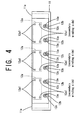
- Fig. 4 shows the inverter substrate 12 in a state of being inserted between the rails 11b, as viewed from the side of the pattern surface.
- through-lead-wires 12a1 of the inverter transformers 12a penetrate to the pattern surface of the inverter substrate 12.
- through-terminals which are arranged adjacent the lower side of the inverter substrate 12 are connected to the secondary side windings.
- through-terminals on the primary side and through-terminals on the secondary side are provided at the opposite sides of a rectangle-shaped body of the inverter transformer.
- the mounting direction of the inverter transformers 12a is determined in such a manner that the through-lead-wires 12a1 on the secondary side are arranged at the same height and lined up along the lower side of the inverter substrate 12.
- the above-mentioned structure allows lengths of wires connected between the cold cathode tubes 13 and the secondary sides of the inverter transformers 12a to be reduced and can prevent a leakage current.
- the inverter substrate 12 can be compactly formed in a thickness direction of the lighting unit 10 and the lighting unit 10 can be made thinner.
- the lighting unit 10 is used as a backlight of a liquid crystal television, the liquid crystal television can be made thinner.
- the inverter transformers 12a are of a back-mounted-type in this embodiment, surface-mounted-type inverter transformers 12a may be mounted on the pattern surface.
- the inverter substrate 12 is formed at the lower side thereof with six notches 12b having shapes upwardly cut deep.
- the notches 12b are each cut in a substantially U-shape in such a manner that a topmost part thereof is made curved.
- Solder pads 12c in which copper patterns are exposed to the outside are formed around the notches 12b.
- the respective solder pads 12c are electrically connected to the secondary side through-lead-wires 12a1 through the copper patterns (not shown) covered with permanent resists.
- the copper patterns which make the connection between the respective solder pads 12c and the secondary side through-lead-wires 12a1 correspond to an electrical supply pattern in this invention.
- the inverter substrate 12 When the inverter substrate 12 is slid downward along the rails 11b until the lower side of the inverter substrate 12 reaches the bottom surface of the reflector panel 11, the respective terminals 13a of the cold cathode tubes 13 are received into corresponding notches 12b and then abutted against the curved topmost parts of the notches 12b.
- the topmost parts are each formed in an upwardly protruding and curved line, so that even if the respective terminals 13a are shifted, they can be guided into the topmost parts of the notches 12b. Moreover, even if the terminals 13a are lifted up, they can be pressed down by the inverter substrate 12 which is slid from the upward direction.
- solder pads 12c are subjected to soldering.
- Fig. 5 shows solders 12d which are formed at the solder pads 12c.
- the solders 12d are formed so as to extend over the terminals 13a penetrating the topmost parts of the notches 12b, and the solder pads 12c, so that the terminals 13a and the solder pads 12c are electrically connected to each other.
- solders 12d are formed at all the solder pads 12c.
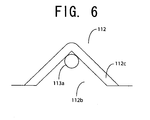
- Fig. 6 shows a part of a modification of the inverter substrate.
- an inverter substrate 112 according to the modification is formed at a lower side thereof with notches 112b (only one notch 112b is shown in Fig. 6 ).
- the notches 112b are each formed in a substantially triangle-shape. Even if the notches 112b are each formed in such a shape, the guiding of terminals 113a into crests of the notches 112b can be carried out while causing the terminals 113a to be slid along slopes of the notches 113a.
- the plurality of substantially U-shaped cold cathode tubes are held parallel relative to the reflector panel and the inverter substrate supplies electricity to the cold cathode tubes.
- the cold cathode tube holder causes the cold cathode tubes to be held parallel relative to the reflector panel in such a manner that the terminals provided at the both ends of the cold cathode tubes are arranged in a row along the one side of the reflector panel.
- the substrate holder causes the inverter substrate to be held vertically relative to the reflector panel in such a manner that the lower side of the inverter substrate reaches the position at which the terminals are lined up in the reflector panel.
- the plurality of notches which are upwardly cut deep into the lower side of the inverter substrate are provided.
- the terminals of the cold cathode tubes are inserted in the notches.
- the solders making the electrical connection between the terminals of the cold cathode tubes and the electrical supply pattern formed on the inverter substrate for supplying electricity to the cold cathode tubes.
- the substrate holder comprises the pair of substantially U-shaped rails interposingly hold the both sides of the rectangle-shaped inverter substrate therebetween from the outward direction.
- the rectangle-shaped inverter substrate is interposedly held from the outward direction by the pair of rails of substantially U-shapes in cross-section.
- the inverter substrate can be stably held.
- the electrical supply pattern is electrically connected to the secondary winding sides of the inverter transformers provided at the inverter substrate, and the inverter transformers are mounted on the inverter substrate in such a direction that the terminals on the secondary winding sides are arranged along the lower side of the inverter substrate.
- the electrical supply pattern is electrically connected to the secondary winding sides of the inverter transformers provided at the inverter substrate, so that AC electricity on the secondary sides is supplied to the cold cathode tubes.
- the inverter transformers are mounted on the inverter substrate in such a direction that the terminals on the secondary winding sides are arranged along the lower side of the inverter substrate.
- a liquid crystal display comprising: a reflector panel; a plurality of substantially U-shaped cold cathode tubes held parallel relative to the reflector panel; an inverter substrate formed in a substantially rectangular shape for supplying electricity to the cold cathode tubes; inverter transformers mounted on the inverter substrate in such a direction that lead wires from secondary winding sides are arranged along the lower side of the inverter substrate; cold cathode tube holders for holding the cold cathode tubes parallel relative to the reflector panel in such a manner that terminals of the cold cathode tubes are arranged in a row along one side of the reflector panel; a substrate holder for holding the inverter substrate to be vertically relative to the reflector panel in such a manner that a lower side of the inverter substrate reaches a positions where the terminals are arranged in a row, the substrate holder comprising a
- the inverter substrate has a plurality of notches for receiving the first terminals and solders.
- the notches are upwardly cut deep into the lower side of the inverter substrate so as to be disposed along the lower side of the inverter substrate, and the solders are for making electrical connections between the second terminals on the secondary winding sides and the electrical supply pattern in the notches.
- the labels such as left, right, front, back, top, bottom, forward, reverse, clockwise, counter clockwise, up, down, or other similar terms such as upper, lower, aft, fore, vertical, horizontal, proximal, distal, etc. have been used for convenience purposes only and are not intended to imply any particular fixed direction or orientation. Instead, they are used to reflect relative locations and/or directions/orientations between various portions of an object.
Landscapes
- Physics & Mathematics (AREA)
- Nonlinear Science (AREA)
- Mathematical Physics (AREA)
- Chemical & Material Sciences (AREA)
- Crystallography & Structural Chemistry (AREA)
- General Physics & Mathematics (AREA)
- Optics & Photonics (AREA)
- Liquid Crystal (AREA)
- Planar Illumination Modules (AREA)
- Arrangement Of Elements, Cooling, Sealing, Or The Like Of Lighting Devices (AREA)
- Fastening Of Light Sources Or Lamp Holders (AREA)
- Non-Portable Lighting Devices Or Systems Thereof (AREA)
Abstract
Description
- The present invention relates to a liquid crystal display apparatus and a lighting unit and, more particularly, to a liquid crystal display apparatus and a lighting unit, in which a plurality of substantially U-shaped cold cathode tubes to which electricity is supplied by an inverter substrate are held parallel relative to a reflector panel.
- An
Japanese Patent Application Laid-Open No. 2002-324592 - The above-mentioned lighting unit is of a type in which one of terminals of the straight cold cathode tube is connected to a small-sized common wiring substrate to which the terminal of the cold cathode tube is to be connected, and is not of a type in which the terminal of the cold cathode tube is connected directly to an inverter substrate. A wire for causing the inverter substrate to be connected to the common wiring substrate is required, so that there is a problem that a leakage current is produced in the wire. The common wiring substrate is satisfied by only providing a common wiring, so that the common wiring substrate may be made thinner. However, the inverter substrate is provided with an inverter circuit, so that the inverter substrate may not be made thinner. Therefore, it is necessary to contrive to stably hold the inverter substrate and contrive to prevent a thickness of the lighting unit from increasing. Moreover, in a case where the above-mentioned technology is applied to a U-shaped cold cathode tube, there is a problem that, when one of terminals provided at both ends of the U-shaped cold cathode tube is subjected to soldering, the other of the terminals rises up from the common wiring substrate and is hard to be subjected to the soldering.
- One aspect of the present invention is directed to a lighting unit which comprises: a reflector panel; a plurality of substantially U-shaped cold cathode tubes held parallel relative to the reflector panel, the substantially U-shaped cold cathode tubes being provided at both ends thereof with terminals; an inverter substrate for supplying electricity to the substantially U-shaped cold cathode tubes, the inverter substrate being provided with an electrical supply pattern for supplying the electricity to the cold cathode tubes; cold cathode tube holder for causing the cold cathode tubes to be held parallel relative to the reflector panel in such a manner that the terminals of the cold cathode tubes are arranged in a row along one side of the reflector panel; and substrate holder for causing the inverter substrate to be held vertically relative to the reflector panel in such a manner that a lower side of the inverter substrate reaches a position at which the terminals are lined up in the reflector panel.
In this lighting unit, the inverter substrate has a plurality of notches for receiving the terminals, the notches being upwardly cut deep into the lower side of the inverter substrate so as to be disposed along the lower side of the inverter substrate, and solders provided for making electrical connections between the terminals and the electrical supply pattern in the notches. - These and other features, aspects, and advantages of the invention will be apparent to those skilled in the art from the following detailed description of preferred non-limiting exemplary embodiments, taken together with the drawings and the claims that follow.
- It is to be understood that the drawings are to be used for the purposes of exemplary illustration only and not as a definition of the limits of the invention. Throughout the disclosure, the word "exemplary" is used exclusively to mean "serving as an example, instance, or illustration." Any embodiment described as "exemplary" is not necessarily to be construed as preferred or advantageous over other embodiments.
Referring to the drawings in which like reference character(s) present corresponding parts throughout: -
-
Fig. 1 is an exemplary exploded perspective view of a lighting unit (liquid crystal display apparatus); -
Fig. 2 is an exemplary perspective view of a reflector panel; -
Fig. 3 is an exemplary perspective view of the reflector panel, in which cold cathode tubes are set with respect to the reflector panel; -
Fig. 4 is an exemplary rear view of an inverter substrate; -
Fig. 5 is an exemplary perspective view of solders which are provided at the inverter substrate; and -
Fig. 6 is an exemplary rear view of a modification of the inverter substrate ofFig. 5 . - The detailed description set forth below in connection with the appended drawings is intended as a description of presently preferred embodiments of the invention and is not intended to represent the only forms in which the present invention may be constructed and/or utilized.
- Embodiments of this invention will be discussed hereinafter in the following order.
- A. First embodiment;
- B. Modification; and
- C. Summary.
-
Fig. 1 shows a lighting unit according to an embodiment of the present invention, as viewed from an oblique direction. In the example shown in the same Figure, thelighting unit 10 generally includes areflector panel 11, aninverter substrate 12, threecold cathode tubes 13, and adiffusion plate 14. Thereflector panel 11 is formed in a shape of a substantially box having a thin thickness and opened upward. An inner surface of thereflector panel 11 has a high reflectance. Thediffusion panel 14 is mounted on thereflector panel 11 so as to put the lid on thereflector plate 11. Moreover, a liquid crystal panel (not shown in drawings) is mounted from the outside of thediffusion plate 14, whereby a liquid crystal display apparatus is formed. -
Fig. 2 shows thereflector panel 11, as viewed from the oblique direction. In the example shown in the same Figure, thereflector panel 11 is provided with a plurality of coldcathode tube holder 11a which are each projected upward in a substantially Y-shape therefrom. At one side of thereflector panel 11, there are provided a pair ofrails 11b of substantially U-shapes in cross-section (substrate holder) which are protrusively provided so as to extend vertically. These rails face inward relative to each other. -
Fig. 3 shows thereflector panel 11, in a condition where thecold cathode tubes 13 are set with respect to thereflector panel 11, as viewed from the oblique direction. In the example shown in the same Figure, thecold cathode tubes 13 are parallel relative to one another and the orientation of thecold cathode tubes 13 is arranged such thatterminals 13a provided at both ends of thecold cathode tubes 13 are located on the side, to which therails 11b are provided, of thereflector panel 11. The coldcathode tube holder 11a are provided at positions that allow some of the coldcathode tube holder 11a to support portions of thecold cathode tubes 13, which are adjacent the terminals thereof, from a downward direction, and at positions that allow some of the coldcathode tubes holder 11a to support bent portions of thecold cathode tubes 13 from the downward direction. - The respective cold
cathode tube holder 11a are formed so as to have the same height, so that the respectivecold cathode tubes 13 are held parallel to a bottom surface of thereflector panel 11. When thecold cathode tubes 13 are held by the coldcathode tube holder 11a, therespective terminals 13a are arranged in a row on the side, to which therails 11b are provided, of thereflector panel 11, and are brought to a condition of being lifted up to a predetermined height from the bottom surface of thereflector plate 11. - The
inverter substrate 12, which is formed in a rectangle-shape as shown inFig. 1 , is interposed at short sides thereof between therails 11b, from an outward direction. More particularly, theinverter substrate 12 is inserted between therails 11b in such a manner that a lower side of theinverter substrate 12 reaches the bottom surface of thereflector panel 11 by causing the short sides of theinverter substrate 12 to be slid downward along therails 11b. Thus, theinverter substrate 12 is held vertically relative to thereflector panel 11. On a parts-mounted surface of theinverter substrate 12, substantially rectangle-shaped inverter transformers 12a are mounted. - The
inverter transformers 12a are provided so as to positionally correspond to thecold cathode tubes 13, and provided with primary side windings and secondary side windings (not shown). Inputting to the primary side windings oscillation pulses generated by a oscillating circuit (not shown) which is provided at theinverter substrate 12 makes it possible to obtain AC which can be outputted to the respectivecold cathode tubes 13 from the secondary side windings. Theinverter substrate 12 is inserted between therails 11b with the parts-mounted surface thereof facing inwardly of thereflector panel 11 and with an opposite pattern surface thereof facing outwardly of thereflector panel 11. -
Fig. 4 shows theinverter substrate 12 in a state of being inserted between therails 11b, as viewed from the side of the pattern surface. In the example shown in the same Figure, through-lead-wires 12a1 of theinverter transformers 12a penetrate to the pattern surface of theinverter substrate 12. Among the through-terminals, through-terminals which are arranged adjacent the lower side of theinverter substrate 12 are connected to the secondary side windings. Generally, in each of theinverter transformers 12a, through-terminals on the primary side and through-terminals on the secondary side are provided at the opposite sides of a rectangle-shaped body of the inverter transformer. In the illustrated embodiment, the mounting direction of theinverter transformers 12a is determined in such a manner that the through-lead-wires 12a1 on the secondary side are arranged at the same height and lined up along the lower side of theinverter substrate 12. - The above-mentioned structure allows lengths of wires connected between the
cold cathode tubes 13 and the secondary sides of theinverter transformers 12a to be reduced and can prevent a leakage current. Moreover, theinverter substrate 12 can be compactly formed in a thickness direction of thelighting unit 10 and thelighting unit 10 can be made thinner. When thelighting unit 10 is used as a backlight of a liquid crystal television, the liquid crystal television can be made thinner. Incidentally, while theinverter transformers 12a are of a back-mounted-type in this embodiment, surface-mounted-type inverter transformers 12a may be mounted on the pattern surface. - The
inverter substrate 12 is formed at the lower side thereof with sixnotches 12b having shapes upwardly cut deep. Thenotches 12b are each cut in a substantially U-shape in such a manner that a topmost part thereof is made curved.Solder pads 12c in which copper patterns are exposed to the outside are formed around thenotches 12b. Therespective solder pads 12c are electrically connected to the secondary side through-lead-wires 12a1 through the copper patterns (not shown) covered with permanent resists. The copper patterns which make the connection between therespective solder pads 12c and the secondary side through-lead-wires 12a1 correspond to an electrical supply pattern in this invention. - When the
inverter substrate 12 is slid downward along therails 11b until the lower side of theinverter substrate 12 reaches the bottom surface of thereflector panel 11, therespective terminals 13a of thecold cathode tubes 13 are received intocorresponding notches 12b and then abutted against the curved topmost parts of thenotches 12b. The topmost parts are each formed in an upwardly protruding and curved line, so that even if therespective terminals 13a are shifted, they can be guided into the topmost parts of thenotches 12b. Moreover, even if theterminals 13a are lifted up, they can be pressed down by theinverter substrate 12 which is slid from the upward direction. Even if the substantially U-shapedcold cathode tubes 13 are inclined, theterminals 13a provided at the both ends of the cold cathode tubes are simultaneously pressed down at the same height, the inclination of thecold cathode tubes 13 in a width direction thereof can be cancelled. - After the insertion of the
inverter substrate 12 is completed in the above-mentioned manner, thesolder pads 12c are subjected to soldering.Fig. 5 showssolders 12d which are formed at thesolder pads 12c. In the example shown in the same Figure, thesolders 12d are formed so as to extend over theterminals 13a penetrating the topmost parts of thenotches 12b, and thesolder pads 12c, so that theterminals 13a and thesolder pads 12c are electrically connected to each other.Such solders 12d are formed at all thesolder pads 12c. Thus, electrical connection is made between thecold cathode tubes 13 and theinverter substrate 12, and theinverter substrate 12 is firmly fixed to thereflector panel 11. -
Fig. 6 shows a part of a modification of the inverter substrate. Like the above-mentioned embodiment, aninverter substrate 112 according to the modification is formed at a lower side thereof withnotches 112b (only onenotch 112b is shown inFig. 6 ). In this modification, thenotches 112b are each formed in a substantially triangle-shape. Even if thenotches 112b are each formed in such a shape, the guiding ofterminals 113a into crests of thenotches 112b can be carried out while causing theterminals 113a to be slid along slopes of thenotches 113a. - As discussed above, in the lighting unit according to the present invention, the plurality of substantially U-shaped cold cathode tubes are held parallel relative to the reflector panel and the inverter substrate supplies electricity to the cold cathode tubes. The cold cathode tube holder causes the cold cathode tubes to be held parallel relative to the reflector panel in such a manner that the terminals provided at the both ends of the cold cathode tubes are arranged in a row along the one side of the reflector panel. The substrate holder causes the inverter substrate to be held vertically relative to the reflector panel in such a manner that the lower side of the inverter substrate reaches the position at which the terminals are lined up in the reflector panel. At the lower side of the inverter substrate which reaches the position at which the terminals are lined up in the reflector panel, the plurality of notches which are upwardly cut deep into the lower side of the inverter substrate are provided. The terminals of the cold cathode tubes are inserted in the notches. In the notches, there are provided the solders making the electrical connection between the terminals of the cold cathode tubes and the electrical supply pattern formed on the inverter substrate for supplying electricity to the cold cathode tubes. By constructing as discussed above, it is possible to provide a liquid crystal display apparatus and a lighting unit, in which leakage current between the inverter substrate and the cold cathode tubes is reduced.
- Moreover, according to the embodiment of the present invention, the substrate holder comprises the pair of substantially U-shaped rails interposingly hold the both sides of the rectangle-shaped inverter substrate therebetween from the outward direction. The rectangle-shaped inverter substrate is interposedly held from the outward direction by the pair of rails of substantially U-shapes in cross-section. Thus, the inverter substrate can be stably held.
- Moreover, according to the embodiment of the present invention, the electrical supply pattern is electrically connected to the secondary winding sides of the inverter transformers provided at the inverter substrate, and the inverter transformers are mounted on the inverter substrate in such a direction that the terminals on the secondary winding sides are arranged along the lower side of the inverter substrate. The electrical supply pattern is electrically connected to the secondary winding sides of the inverter transformers provided at the inverter substrate, so that AC electricity on the secondary sides is supplied to the cold cathode tubes. As discussed above, the inverter transformers are mounted on the inverter substrate in such a direction that the terminals on the secondary winding sides are arranged along the lower side of the inverter substrate. Such a structure makes it possible to reduce the wiring length of the electrical supply pattern and make the lighting unit thinner.
- The present invention may be embodied as a liquid crystal display apparatus which employs the above-mentioned structure. As the embodiment, there is provided with A liquid crystal display comprising: a reflector panel; a plurality of substantially U-shaped cold cathode tubes held parallel relative to the reflector panel; an inverter substrate formed in a substantially rectangular shape for supplying electricity to the cold cathode tubes;
inverter transformers mounted on the inverter substrate in such a direction that lead wires from secondary winding sides are arranged along the lower side of the inverter substrate; cold cathode tube holders for holding the cold cathode tubes parallel relative to the reflector panel in such a manner that terminals of the cold cathode tubes are arranged in a row along one side of the reflector panel; a substrate holder for holding the inverter substrate to be vertically relative to the reflector panel in such a manner that a lower side of the inverter substrate reaches a positions where the terminals are arranged in a row, the substrate holder comprising a pair of substantially U-shaped rails interposingly holding opposite sides of the inverter substrate; a plurality of notches upwardly cut deep from the lower side of the inverter substrate so as to receive the terminals; and
solders provided for making electrical connections between the terminals and electrical supply patterns formed in the notches.
The inverter substrate has a plurality of notches for receiving the first terminals and solders. The notches are upwardly cut deep into the lower side of the inverter substrate so as to be disposed along the lower side of the inverter substrate, and the solders are for making electrical connections between the second terminals on the secondary winding sides and the electrical supply pattern in the notches. Such a structure makes it possible to provide a liquid crystal display apparatus and lighting unit in which leakage current between the inverter substrate and the cold cathode tubes is reduced. - Although the invention has been described in considerable detail in language specific to structural features or method acts, it is to be understood that the invention defined in the appended claims is not necessarily limited to the specific features or acts described. Rather, the specific features and acts are disclosed as preferred forms of implementing the claimed invention. Therefore, while exemplary illustrative embodiments of the invention have been described, numerous variations and alternative embodiments will occur to those skilled in the art. Such variations and alternate embodiments are contemplated, and can be made without departing from the spirit and scope of the invention.
- It is to be understood that the phraseology and terminology employed herein, as well as the abstract, are for the purpose of description and should not be regarded as limiting.
- It should further be noted that throughout the entire disclosure, the labels such as left, right, front, back, top, bottom, forward, reverse, clockwise, counter clockwise, up, down, or other similar terms such as upper, lower, aft, fore, vertical, horizontal, proximal, distal, etc. have been used for convenience purposes only and are not intended to imply any particular fixed direction or orientation. Instead, they are used to reflect relative locations and/or directions/orientations between various portions of an object.
- In addition, reference to "first," "second," "third," and etc. members throughout the disclosure (and in particular, claims) is not used to show a serial or numerical limitation but instead is used to distinguish or identify the various members of the group.
Claims (4)
- A lighting unit having a reflector panel, a plurality of substantially U-shaped cold cathode tubes held parallel relative to the reflector panel and an inverter substrate for supplying electricity to the cold cathode tubes characterized in that the lighting unit comprising:cold cathode tube holders for holding the cold cathode tubes parallel relative to the reflector panel with terminals of the cold cathode tubes arranged in a row along one side of the reflector panel;a substrate holder for holding the inverter substrate to be vertically relative to the reflector panel with a lower side of the inverter substrate reaching a position where the terminals are arranged in a row;a plurality of notches upwardly cut deep from the lower side of the inverter substrate so as to receive the terminals; andsolders provided for making electrical connections between the terminals and electrical supply patterns formed in the notches.
- A lighting unit as set forth claim 1, characterized in that:the inverter substrate is formed in a rectangle-shape, and the substrate holder comprises a pair of rails having substantially U-shapes in cross-section and interposingly holding opposite sides of the rectangle-shaped inverter substrate.
- A lighting unit as set forth claim 1 or 2, characterized in that:the inverter substrate is provided with inverter transformers, the inverter transformers is provided with lead wires from secondary winding sides are arranged along the lower side of the inverter substrate, and the electrical supply pattern is electrically connected to the lead wires.
- A liquid crystal display having a reflector panel, a plurality of substantially U-shaped cold cathode tubes held parallel relative to the reflector panel and an inverter substrate formed in a substantially rectangular shape for supplying electricity to the cold cathode tubes characterized in that the lighting unit comprising:inverter transformers mounted on the inverter substrate with lead wires from secondary winding sides arranged along the lower side of the inverter substrate;cold cathode tube holders for holding the cold cathode tubes parallel relative to the reflector panel with terminals of the cold cathode tubes arranged in a row along one side of the reflector panel;a substrate holder for holding the inverter substrate to be vertically relative to the reflector panel with a lower side of the inverter substrate reaching a position where the terminals are arranged in a row, the substrate holder comprising a pair of substantially U-shaped rails interposingly holding opposite sides of the inverter substrate;a plurality of notches upwardly cut deep from the lower side of the inverter substrate so as to receive the terminals; andsolders provided for making electrical connections between the terminals and electrical supply patterns formed in the notches.
Applications Claiming Priority (1)
| Application Number | Priority Date | Filing Date | Title |
|---|---|---|---|
| JP2007001611A JP4288523B2 (en) | 2007-01-09 | 2007-01-09 | Liquid crystal display device and lighting unit |
Publications (2)
| Publication Number | Publication Date |
|---|---|
| EP1944647A1 true EP1944647A1 (en) | 2008-07-16 |
| EP1944647B1 EP1944647B1 (en) | 2009-08-05 |
Family
ID=39204597
Family Applications (1)
| Application Number | Title | Priority Date | Filing Date |
|---|---|---|---|
| EP08000177A Not-in-force EP1944647B1 (en) | 2007-01-09 | 2008-01-07 | Liquid crystal display apparatus and lighting unit |
Country Status (4)
| Country | Link |
|---|---|
| US (1) | US7748885B2 (en) |
| EP (1) | EP1944647B1 (en) |
| JP (1) | JP4288523B2 (en) |
| DE (1) | DE602008000064D1 (en) |
Families Citing this family (5)
| Publication number | Priority date | Publication date | Assignee | Title |
|---|---|---|---|---|
| US8064005B2 (en) * | 2008-07-31 | 2011-11-22 | Samsung Electronics Co., Ltd. | Light supplying unit and display device using the same |
| JP5355325B2 (en) * | 2009-09-17 | 2013-11-27 | パナソニック液晶ディスプレイ株式会社 | Liquid crystal display |
| US20120218478A1 (en) * | 2009-11-06 | 2012-08-30 | Sharp Kabushiki Kaisha | Lighting device, display device and television receiver |
| US20140347599A1 (en) * | 2013-05-24 | 2014-11-27 | Hon Hai Precision Industry Co., Ltd. | Backlight module and liquid crystal display device |
| US9949051B2 (en) * | 2015-06-04 | 2018-04-17 | Starkey Laboratories, Inc. | Embedded and printed acoustic port |
Citations (4)
| Publication number | Priority date | Publication date | Assignee | Title |
|---|---|---|---|---|
| JP2002324592A (en) | 2001-04-26 | 2002-11-08 | Stanley Electric Co Ltd | Connection structure of electrode wire of cold cathode tube for surface light source |
| US20040027049A1 (en) * | 2002-08-09 | 2004-02-12 | Hea-Chun Lee | Lamp assembly, light supplying apparatus and liquid crystal display device using the same |
| US20060092633A1 (en) * | 2004-11-04 | 2006-05-04 | Lg. Philips Lcd Co., Ltd. | Back light unit |
| US20060221607A1 (en) * | 2005-04-01 | 2006-10-05 | Innolux Display Corp. | Backlight assembly for liquid crystal display |
Family Cites Families (5)
| Publication number | Priority date | Publication date | Assignee | Title |
|---|---|---|---|---|
| JP2564565Y2 (en) | 1991-06-25 | 1998-03-09 | 日本電気エンジニアリング株式会社 | Fluorescent tube holding device |
| JP2001076529A (en) | 1999-09-01 | 2001-03-23 | Sharp Corp | Backlight power supply unit and backlight unit for liquid crystal display device using the same |
| KR100442297B1 (en) * | 2002-06-14 | 2004-07-30 | 엘지.필립스 엘시디 주식회사 | Back light |
| US7686498B2 (en) * | 2004-12-28 | 2010-03-30 | Sharp Kabushiki Kaisha | Support structure for a light source, a backlight unit for a display device having the support structure, and a display device |
| JP4552089B2 (en) * | 2005-09-09 | 2010-09-29 | ミネベア株式会社 | Backlight device and liquid crystal display device |
-
2007
- 2007-01-09 JP JP2007001611A patent/JP4288523B2/en not_active Expired - Fee Related
-
2008
- 2008-01-07 US US12/006,914 patent/US7748885B2/en not_active Expired - Fee Related
- 2008-01-07 DE DE602008000064T patent/DE602008000064D1/en active Active
- 2008-01-07 EP EP08000177A patent/EP1944647B1/en not_active Not-in-force
Patent Citations (4)
| Publication number | Priority date | Publication date | Assignee | Title |
|---|---|---|---|---|
| JP2002324592A (en) | 2001-04-26 | 2002-11-08 | Stanley Electric Co Ltd | Connection structure of electrode wire of cold cathode tube for surface light source |
| US20040027049A1 (en) * | 2002-08-09 | 2004-02-12 | Hea-Chun Lee | Lamp assembly, light supplying apparatus and liquid crystal display device using the same |
| US20060092633A1 (en) * | 2004-11-04 | 2006-05-04 | Lg. Philips Lcd Co., Ltd. | Back light unit |
| US20060221607A1 (en) * | 2005-04-01 | 2006-10-05 | Innolux Display Corp. | Backlight assembly for liquid crystal display |
Also Published As
| Publication number | Publication date |
|---|---|
| JP4288523B2 (en) | 2009-07-01 |
| DE602008000064D1 (en) | 2009-09-17 |
| US7748885B2 (en) | 2010-07-06 |
| US20080165305A1 (en) | 2008-07-10 |
| EP1944647B1 (en) | 2009-08-05 |
| JP2008170548A (en) | 2008-07-24 |
Similar Documents
| Publication | Publication Date | Title |
|---|---|---|
| US20060279957A1 (en) | Lamp, lamp holder, power supply module, backlight assembly having the power supply module and display device having the power supply module | |
| US7116204B2 (en) | Leakage transformer | |
| CN101051142B (en) | Backlight assembly and liquid crystal display thereof | |
| EP1944647B1 (en) | Liquid crystal display apparatus and lighting unit | |
| EP1912094A1 (en) | Backlight assembly and display apparatus having the same | |
| EP1884822A1 (en) | Side mold for backlight assembly, backlight assembly, assembly method thereof, and liquid crystal display | |
| TW200814470A (en) | Lamp socket, backlight assembly having the same and display device having the same | |
| JP2008117772A (en) | Lamp socket and backlight assembly having the same | |
| KR100794082B1 (en) | High Voltage Base and Socket Connectors | |
| JP2000150054A (en) | Joint connector | |
| JP2010282856A (en) | LCD module | |
| CN100463299C (en) | Connector and liquid crystal display device using the same | |
| JP2003185995A (en) | Liquid crystal display | |
| EP2149814B1 (en) | Light supplying unit and display device using the same | |
| JP2005253173A (en) | Production process of electric connection box | |
| JP2001176581A (en) | Terminal, connection structure of fluorescent electrode rod-shaped electrode and conducting core wire, surface light source device and image display device | |
| CN100589292C (en) | Connector device and backlight assembly using the same | |
| JP2003338342A (en) | Printed wiring board connector | |
| JP2007036036A (en) | Terminal box for solar cell module | |
| JP2004302048A (en) | Liquid crystal display device | |
| JP2001244015A (en) | Joint connector | |
| JP2005236206A (en) | Solar cell module and terminal box | |
| JP2002324592A (en) | Connection structure of electrode wire of cold cathode tube for surface light source | |
| JPH08202276A (en) | Liquid crystal display | |
| JP2596741Y2 (en) | Battery terminal spring mounting device |
Legal Events
| Date | Code | Title | Description |
|---|---|---|---|
| PUAI | Public reference made under article 153(3) epc to a published international application that has entered the european phase |
Free format text: ORIGINAL CODE: 0009012 |
|
| AK | Designated contracting states |
Kind code of ref document: A1 Designated state(s): AT BE BG CH CY CZ DE DK EE ES FI FR GB GR HR HU IE IS IT LI LT LU LV MC MT NL NO PL PT RO SE SI SK TR |
|
| AX | Request for extension of the european patent |
Extension state: AL BA MK RS |
|
| 17P | Request for examination filed |
Effective date: 20080808 |
|
| 17Q | First examination report despatched |
Effective date: 20080912 |
|
| GRAP | Despatch of communication of intention to grant a patent |
Free format text: ORIGINAL CODE: EPIDOSNIGR1 |
|
| AKX | Designation fees paid |
Designated state(s): DE FR GB |
|
| GRAS | Grant fee paid |
Free format text: ORIGINAL CODE: EPIDOSNIGR3 |
|
| GRAA | (expected) grant |
Free format text: ORIGINAL CODE: 0009210 |
|
| AK | Designated contracting states |
Kind code of ref document: B1 Designated state(s): DE FR GB |
|
| REG | Reference to a national code |
Ref country code: GB Ref legal event code: FG4D |
|
| REF | Corresponds to: |
Ref document number: 602008000064 Country of ref document: DE Date of ref document: 20090917 Kind code of ref document: P |
|
| PLBE | No opposition filed within time limit |
Free format text: ORIGINAL CODE: 0009261 |
|
| STAA | Information on the status of an ep patent application or granted ep patent |
Free format text: STATUS: NO OPPOSITION FILED WITHIN TIME LIMIT |
|
| 26N | No opposition filed |
Effective date: 20100507 |
|
| REG | Reference to a national code |
Ref country code: FR Ref legal event code: PLFP Year of fee payment: 9 |
|
| PGFP | Annual fee paid to national office [announced via postgrant information from national office to epo] |
Ref country code: FR Payment date: 20151208 Year of fee payment: 9 |
|
| PGFP | Annual fee paid to national office [announced via postgrant information from national office to epo] |
Ref country code: DE Payment date: 20151229 Year of fee payment: 9 |
|
| PGFP | Annual fee paid to national office [announced via postgrant information from national office to epo] |
Ref country code: GB Payment date: 20160106 Year of fee payment: 9 |
|
| REG | Reference to a national code |
Ref country code: DE Ref legal event code: R119 Ref document number: 602008000064 Country of ref document: DE |
|
| GBPC | Gb: european patent ceased through non-payment of renewal fee |
Effective date: 20170107 |
|
| REG | Reference to a national code |
Ref country code: FR Ref legal event code: ST Effective date: 20170929 |
|
| PG25 | Lapsed in a contracting state [announced via postgrant information from national office to epo] |
Ref country code: FR Free format text: LAPSE BECAUSE OF NON-PAYMENT OF DUE FEES Effective date: 20170131 |
|
| PG25 | Lapsed in a contracting state [announced via postgrant information from national office to epo] |
Ref country code: DE Free format text: LAPSE BECAUSE OF NON-PAYMENT OF DUE FEES Effective date: 20170801 Ref country code: GB Free format text: LAPSE BECAUSE OF NON-PAYMENT OF DUE FEES Effective date: 20170107 |