EP1944266A1 - MEMS Packaging with reduced mechanical strain - Google Patents
MEMS Packaging with reduced mechanical strain Download PDFInfo
- Publication number
- EP1944266A1 EP1944266A1 EP08100173A EP08100173A EP1944266A1 EP 1944266 A1 EP1944266 A1 EP 1944266A1 EP 08100173 A EP08100173 A EP 08100173A EP 08100173 A EP08100173 A EP 08100173A EP 1944266 A1 EP1944266 A1 EP 1944266A1
- Authority
- EP
- European Patent Office
- Prior art keywords
- pillars
- die
- micro
- package
- electromechanical
- Prior art date
- Legal status (The legal status is an assumption and is not a legal conclusion. Google has not performed a legal analysis and makes no representation as to the accuracy of the status listed.)
- Withdrawn
Links
Images



Classifications
-
- B—PERFORMING OPERATIONS; TRANSPORTING
- B81—MICROSTRUCTURAL TECHNOLOGY
- B81B—MICROSTRUCTURAL DEVICES OR SYSTEMS, e.g. MICROMECHANICAL DEVICES
- B81B7/00—Microstructural systems ; Auxiliary parts of microstructural devices or systems
- B81B7/0032—Packages or encapsulation
- B81B7/0045—Packages or encapsulation for reducing stress inside of the package structure
- B81B7/0048—Packages or encapsulation for reducing stress inside of the package structure between the MEMS die and the substrate
Definitions
- the present invention is directed to an improved design for Micro Electro-Mechanical Systems (MEMS) packages. More specifically, the present invention is directed to improvements in how a MEMS die is attached to a package.
- MEMS Micro Electro-Mechanical Systems
- a MEMS die or die assembly which is attached to a package such as a lead frame, substrate or header, will experience mechanical stresses/strains due to a mismatch in the thermal expansion of the materials. These stresses can damage the die or indeed the package to which the die is attached and degrade the MEMS's performance. These stresses/strains will cause very sensitive and precise connections between the MEMS die and the package to become misaligned, thereby creating error signals and various types of malfunctions.
- dies have been introduced where the dies themselves form the support structure.
- These die supports are patterned or etched on one side of the main die using standard photolithography and wet or dry etching methods to form one or more pillars or pedestals.
- These smaller contact surfaces act as stress relief members by their ability to deform and thereby cause reduced stresses into the active part of the MEMS device.
- the present invention provides a micro-electromechanical device comprising:
- the present invention provides a method of minimizing the strain transferred from a package to a MEMS die.
- the first step of this method comprises selecting the minimum contact area (bond area), given the substrate material, die material and bond material and the bonding process in accordance with die shear (strength) test criteria. Such criteria can be found in standards like Mil-Std-883 Method 2019.
- Die Shear Testing is the process of determining the strength of adhesion of a semiconductor die to the package's die attach substrate (such as the die pad of a lead frame or the cavity of a hermetic package), by subjecting the die to a stress that's parallel to the plane of the die attach substrate, resulting in a shearing stress between the die-die attach material interface and the die attach material-substrate interface.
- the package's die attach substrate such as the die pad of a lead frame or the cavity of a hermetic package
- the general purpose of die shear testing is to assess the over-all quality of the die attach process, including the integrity of the materials and the capabilities of the processes used in mounting the die (and other elements, if any) to the package substrate.
- Mil-Std-883 Method 2019 is the most widely-used industry standard for performing this test.
- a typical die shear tester consists of: 1) a mechanism that applies the correct load to the die with an accuracy of +/- 5% of full scale or 50 g (the greater of these tolerances); 2) a die contact tool which makes the actual contact with the full length of the die edge to apply the force uniformly from one end of the edge to the other; 3) provisions to ensure that the die contact tool is perpendicular to the die attach plane; 4) provisions to ensure that the fixture holding the die may be rotated with respect to the contact tool so that the die edge and contact tool may always be aligned in parallel to each other; and 5) a binocular microscope (10X min magnification) and lighting system to facilitate the observation of the die and contact tool while the test is being performed.
- the force applied to the die during die shear testing must be sufficient to shear the die from its mounting or twice the lower specification limit for the die shear strength (whichever occurs first).
- the direction of the applied force must be perpendicular to the die edge and parallel to the die attach or substrate plane. After the initial contact has been made and the application of force starts, the relative position of the tool must not change vertically (i.e. It must be prevented from contacting either the die attach material or the substrate).
- Failures from die shear testing include: 1) failure to meet the specified die shear strength requirements; 2) a separation that occurs at less than 1.25X the minimum die shear strength and evidence of less than 50% adhesion of the die attach material; and 3) a separation that occurs at less than 2X the minimum die shear strength and evidence of less than 10% adhesion of the die attach material.
- the mode of separation must also be classified into and recorded as any of the following: 1) shearing of the die itself with silicon remaining; 2) separation of the die from the die attach material; and 3) separation of both the die and die attach material from the package substrate.
- the second step in the method comprises selecting the minimum applicable feature size for the footprint given the bonding process, the bond material and the bondline thickness.
- the minimum dimension to be supported of the bondline through the bonding process may be assumed to be 10x the bondline (i.e. 100 micrometers).
- the actual footprint (area of the pillars) must obviously support the die in the bonding material (non cured) and not push the material away, thereby not leaving any bondline thickness.
- the reason for establishing the minimum dimension (in one direction) is to position the most compliant direction of the pillar in the direction of maximum strain.
- the minimum cross section A x B is given by the needed strength of the bonding technology used (gluing, anodic bonding, eutectic seal or similar). Therefore, optimum stress relief is by addressing the direction with the "worst" elongate mismatch and minimizing the thickness of the stand in this direction according to what is practically possible given the device and the manufacturing processes. Also, the height (H) of the stand should always be maximized according to what is practically possible given the device and the manufacturing processes.
- the third step in the method comprises establishing the full geometrical shape for the pillars given the material and the shaping (manufacturing) process.
- the fourth step of the method comprises calculating the position of orientation.
- the eaxmple problem of thermal expansion will be solved.
- Both the materials used for packages and the materials used for MEMS dies are subject to thermal expansion.
- Thermal expansion can be precisely modelled by selecting a point at the centre of a surface and assuming that the expansion of that surface extends radially from that point.
- a package 10 has an origin 30 and a MEMS die 20 has an origin 40.
- CTE Coefficient of Thermal Expansion
- ⁇ T the change in temperature
- r is the distance of a point from the origin.
- a MEMS die 20 will not be made of the same material as the package 10 to which it is attached.
- the MEMS die 20 and the package 10 will have different CTEs and will therefore be prone to varying degrees of thermal expansion. This creates a problem in that, because the MEMS die 20 is attached to the package 10, this difference in radial deformation will create a strain transferred by the pillars to the MEMS die 20 to the package 10.
- ⁇ 10 is the CTE of the package 10
- ⁇ 20 is the CTE of the MEMS die 20.
- a problem which has been appreciated by the applicant is that, because of the anisotropic crystalline nature of the materials often used for the pillars, although the shearing forces acting on the pillars are all radial, these same radial forces will create tangential strains in the pillars, thereby applying tangential forces to the MEMS die 20.
- each pillar has the same shape and is orientated in the same way with respect to the origin.
- the calculations will be further simplified in that, because of the fact that the pillars are of identical shape and identical orientation with respect to the origin, the material properties of and the forces acting on each pillar can be expressed similarly using a distinct coordinate system for each pillar (i.e. x 1 , y 1 ; x 2 , y 2 and x 3 , y 3 ).
- the force exerted by each pillar will have a radial component and a tangential component.
- the radial components will be k xi r xi and the tangential components will be k yxi r xi .
- the final step in the method of the present invention is to calculate the appropriate minimum height (H) for the pillars according to the maximum allowed stress in relation to the die performance. For example, if a certain function has a calculated known sensitivity to stress in the die, using the pillar solution, this stress may be reduced by the compliance of the pillars. The capacity for the pillars to absorb stress will be inversely proportional to H 3 .
Landscapes
- Engineering & Computer Science (AREA)
- Microelectronics & Electronic Packaging (AREA)
- Computer Hardware Design (AREA)
- Micromachines (AREA)
Abstract
Description
- The present invention is directed to an improved design for Micro Electro-Mechanical Systems (MEMS) packages. More specifically, the present invention is directed to improvements in how a MEMS die is attached to a package.
- A MEMS die or die assembly which is attached to a package such as a lead frame, substrate or header, will experience mechanical stresses/strains due to a mismatch in the thermal expansion of the materials. These stresses can damage the die or indeed the package to which the die is attached and degrade the MEMS's performance. These stresses/strains will cause very sensitive and precise connections between the MEMS die and the package to become misaligned, thereby creating error signals and various types of malfunctions.
- To remedy this problem, long and thick support structures such as thick support dies or long glass tubes have been developed. Unfortunately, these solutions require that the packages themselves be much larger and that the resulting wafer be considerably thicker.
- Recently, dies have been introduced where the dies themselves form the support structure. These die supports are patterned or etched on one side of the main die using standard photolithography and wet or dry etching methods to form one or more pillars or pedestals. These smaller contact surfaces act as stress relief members by their ability to deform and thereby cause reduced stresses into the active part of the MEMS device.
- Thus, what is needed is a MEMS design which comprises support pillars that, under the strain of deformation of a package, will minimise the strain which is transferred to the MEMS die.
- In order to solve the problems associated with the designs of the prior art, the present invention provides a micro-electromechanical device comprising:
- a micro-electromechanical die;
- a package; and
- three pillars attaching the micro-electromechanical die to the package, wherein:
- at least one of the shape, position and orientation of the pillars is such that any strain transferred from the package to the die by deformation of the package is minimised.
- With the arrangement of the present invention it is possible to instruct a MEMS device which has a minimal amount of stress and/or strain applied to the actual device both during manufacture and during operation yet which is still simple and cost effective to manufacture.
- An example of the present invention will now be described with reference to the accompanying drawings in which:
-
Figure 1 represents a flow chart of the method of the present invention; -
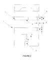
Figure 2 represents a side and bottom view of the pillar arrangement in accordance with one embodiment of the present invention; -
Figure 3 represents the radial expansion model of a die and a package; -
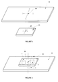
Figure 4 represents a 3-dimensional view of a pillar arrangement in accordance with the present invention; -
Figure 5 represents a planar view of the spacial arrangement of pillars in accordance with the present invention; and -
Figure 6 represents a planar view of radial an tangential forces induced in pillars in accordance with the present invention. - In reference to
Figure 1 , the present invention provides a method of minimizing the strain transferred from a package to a MEMS die. The first step of this method comprises selecting the minimum contact area (bond area), given the substrate material, die material and bond material and the bonding process in accordance with die shear (strength) test criteria. Such criteria can be found in standards like Mil-Std-883 Method 2019. - Die Shear Testing is the process of determining the strength of adhesion of a semiconductor die to the package's die attach substrate (such as the die pad of a lead frame or the cavity of a hermetic package), by subjecting the die to a stress that's parallel to the plane of the die attach substrate, resulting in a shearing stress between the die-die attach material interface and the die attach material-substrate interface.
- The general purpose of die shear testing is to assess the over-all quality of the die attach process, including the integrity of the materials and the capabilities of the processes used in mounting the die (and other elements, if any) to the package substrate. Mil-Std-883 Method 2019 is the most widely-used industry standard for performing this test.
- A typical die shear tester consists of: 1) a mechanism that applies the correct load to the die with an accuracy of +/- 5% of full scale or 50 g (the greater of these tolerances); 2) a die contact tool which makes the actual contact with the full length of the die edge to apply the force uniformly from one end of the edge to the other; 3) provisions to ensure that the die contact tool is perpendicular to the die attach plane; 4) provisions to ensure that the fixture holding the die may be rotated with respect to the contact tool so that the die edge and contact tool may always be aligned in parallel to each other; and 5) a binocular microscope (10X min magnification) and lighting system to facilitate the observation of the die and contact tool while the test is being performed.
- The force applied to the die during die shear testing must be sufficient to shear the die from its mounting or twice the lower specification limit for the die shear strength (whichever occurs first). The direction of the applied force must be perpendicular to the die edge and parallel to the die attach or substrate plane. After the initial contact has been made and the application of force starts, the relative position of the tool must not change vertically (i.e. It must be prevented from contacting either the die attach material or the substrate).
- Failures from die shear testing include: 1) failure to meet the specified die shear strength requirements; 2) a separation that occurs at less than 1.25X the minimum die shear strength and evidence of less than 50% adhesion of the die attach material; and 3) a separation that occurs at less than 2X the minimum die shear strength and evidence of less than 10% adhesion of the die attach material.
- The mode of separation must also be classified into and recorded as any of the following: 1) shearing of the die itself with silicon remaining; 2) separation of the die from the die attach material; and 3) separation of both the die and die attach material from the package substrate.
- The second step in the method comprises selecting the minimum applicable feature size for the footprint given the bonding process, the bond material and the bondline thickness.
- For example, if the minimum bondline thicknesses are decided to be typically 10 micrometers, the minimum dimension to be supported of the bondline through the bonding process may be assumed to be 10x the bondline (i.e. 100 micrometers). The actual footprint (area of the pillars) must obviously support the die in the bonding material (non cured) and not push the material away, thereby not leaving any bondline thickness. The reason for establishing the minimum dimension (in one direction) is to position the most compliant direction of the pillar in the direction of maximum strain.
- In reference to
Figure 2 , stress in the die, due to thermal or other effects causing mismatch in physical dimensions of the die in comparison to the substrate on which the die is mounted, will be proportional to the stiffness of the stands. According to general textbook formulas for stress & strain, the stiffness (k) in the stands will be:a) in case mismatch along X direction; k = constant x (B x A3 / H3) b) in case mismatch along Y direction; k = constant x (A x B3 / H3) - Typically, the minimum cross section A x B is given by the needed strength of the bonding technology used (gluing, anodic bonding, eutectic seal or similar). Therefore, optimum stress relief is by addressing the direction with the "worst" elongate mismatch and minimizing the thickness of the stand in this direction according to what is practically possible given the device and the manufacturing processes. Also, the height (H) of the stand should always be maximized according to what is practically possible given the device and the manufacturing processes.
- The third step in the method comprises establishing the full geometrical shape for the pillars given the material and the shaping (manufacturing) process. The fourth step of the method comprises calculating the position of orientation.
- In a first example of the fourth step of the present invention, the eaxmple problem of thermal expansion will be solved. Both the materials used for packages and the materials used for MEMS dies are subject to thermal expansion. Thermal expansion can be precisely modelled by selecting a point at the centre of a surface and assuming that the expansion of that surface extends radially from that point.
- With reference to
Figure 3 , apackage 10 has anorigin 30 and aMEMS die 20 has anorigin 40. The radial displacement (Δx) of a point around the origin of either thepackage 10 or theMEMS die 20 can be approximated by:
where α is the Coefficient of Thermal Expansion (CTE), ΔT is the change in temperature and r is the distance of a point from the origin. Thus, a point which is farther away from the origin will undergo a larger displacement than a point which is nearer to the origin. - In the majority of cases, a
MEMS die 20 will not be made of the same material as thepackage 10 to which it is attached. Thus, typically, the MEMS die 20 and thepackage 10 will have different CTEs and will therefore be prone to varying degrees of thermal expansion. This creates a problem in that, because theMEMS die 20 is attached to thepackage 10, this difference in radial deformation will create a strain transferred by the pillars to theMEMS die 20 to thepackage 10. - The relative radial deformation of the
package 10 with respect to theMEMS die 20 can be approximated by:
where r is the distance from the origine, α10 is the CTE of thepackage 10, α20 is the CTE of theMEMS die 20. Thus, relative deformation between theMEMS die 20 and thepackage 10 will create stress in the pillars in a radial direction. The applicant has appreciated that the pillars should be located as close to the origin as the stability of the die allows. - A problem which has been appreciated by the applicant is that, because of the anisotropic crystalline nature of the materials often used for the pillars, although the shearing forces acting on the pillars are all radial, these same radial forces will create tangential strains in the pillars, thereby applying tangential forces to the MEMS die 20.
- Now, with reference to
Figure 4 , the applicant has also appreciated that the minimum number of pillars which will be needed to support a two dimensional surface is three (1; 2; 3). More than three pillars would unnecessarily complicate the method for balancing the forces acting upon the pillars. Also, in order to further simplify the calculations, for this example each pillar has the same shape and is orientated in the same way with respect to the origin. The calculations will be further simplified in that, because of the fact that the pillars are of identical shape and identical orientation with respect to the origin, the material properties of and the forces acting on each pillar can be expressed similarly using a distinct coordinate system for each pillar (i.e. x1, y1; x2, y2 and x3, y3). - Thus, the spring constant of any one of the pillars in the three pillar design of the present invention can be approximated by:

where i is the pillar number (i.e. 1 to 3), kx is the spring constant in the x direction, ky is the spring constant in the y direction, kxy, is the spring constant in the x direction in relation to a force applied in the y direction and finally, kyx is the spring constant in the y direction in relation to a force applied in the x direction. - Now, using Hookes Law, it can be shown that the forces created in the pillars in response to a relative deformation of the MEMS die 20 with respect to the
package 10 will be as follows:
or
- However, since we assume that the deformation of the material is purely radial, ry, the tangential displacement, will be 0. Thus, the product of these two matrices becomes:

- As shown in
Figure 5 , the force exerted by each pillar will have a radial component and a tangential component. The radial components will be kxi rxi and the tangential components will be kyxi rxi. - The summation of forces gives:

and
where, equations 9 represents the summation of forces in the y3 direction andequation 10 represents the summation of forces in the x3 direction. By combiningequations 9 and 10 and replacing Δx by α·Δt· r, it can be shown that the summation of forces should be equal to:

- Now, again with reference to
Figure 6 and equation 6, the sum of the tangential forces created by the three pillars will give rise to a moment:
- As has been explained above, the tangential forces created in the pillars will be responsible for any rotational displacement of the MEMS die 20 with respect to the
package 10. The moment relating the a tangential force in a pillar can be expressed as follows:
by combiningequations 12 and 13, the sum of the moments can be expressed as follows:
- If the sum of the moments relating to the tangential forces are equal to 0, there will be no rotational displacement of the MEMS die 20 with respect to the
package 10. In order to completely eliminate the rotational movement of the MEMS die 20 relative to thepackage 10, the following equation must be true:
Thus, the material used in fabrication of pillars for MEMS dies 20 can be taken advantage of by positioning the pillars in order to satisfy the following equations:

and
- By satisfying equations 17, 18 and 19, one can position and orient the pillars such that the strain transferred from the package to the die is minimised.
- The final step in the method of the present invention is to calculate the appropriate minimum height (H) for the pillars according to the maximum allowed stress in relation to the die performance. For example, if a certain function has a calculated known sensitivity to stress in the die, using the pillar solution, this stress may be reduced by the compliance of the pillars. The capacity for the pillars to absorb stress will be inversely proportional to H3.
Claims (7)
- A micro-electromechanical device comprising:a micro-electromechanical die (20);a package (10); andthree pillars (1; 2; 3) attaching the micro-electromechanical die to the package, wherein:at least one of the shape, position and orientation of the pillars is such that any strain transferred from the package to the die by deformation of the package is minimised.
- The micro-electromechanical device of claim 1, wherein the pillars are bonded to the package and the shape of the pillars is determined based on the minimum contact area needed, given the package, the micro-electromechanical die and bond materials and the bonding process in accordance with die shear test criteria, as given in specific standards, such as Mil-Std-883 Method 2019.
- The micro-electromechanical device of any of the preceding claims, wherein the shape of the pillars is also determined based on the minimum applicable feature size, given the bonding process, the bond material and the bondline thickness.
- The micro-electromechanical device of any of the preceding claims, wherein the pillars are formed on the die using chemical etching or mechanical abrasion.
- The micro-electromechanical device of any of claims 1 to 3, wherein the pillars are formed on the substrate using patterned electroplating, moulded pillars or mechanical stamping.
- The micro-electromechanical device of any of claims 1 to 3, wherein the pillars are prefabricated and bonded onto the die.
- The micro-electromechanical device according to any of the preceding claims, wherein,
the three pillars are arranged around a point on a surface of the mico-electromechanical die (20);
rx1, rx2 and rx3 are the lengths of first, second and third axes extending from the first, second and third pillars (1; 2; 3) respectively to the point;
kx1, kx2 and kx3 are the spring constants in the radial direction of the point of the first, second and third pillars (1; 2; 3) respectively;
kyx1, kyx2 and kyx3 are the relationships between a deformation of the first, second and third pillars (1; 2; 3) respectively in a direction which is both normal to the radial direction of the central point and parallel to a plane formed by the surface of the micro-electromechanical die (20) and a force applied to the first, second and third pillars (1; 2; 3) respectively in radial direction of the point;
φ 1 and φ2 are the angles separating the first and second axes respectively from the third axis; and
the position of the three pillars satisfy the following equations:

and
Priority Applications (1)
| Application Number | Priority Date | Filing Date | Title |
|---|---|---|---|
| EP08100173A EP1944266A1 (en) | 2007-01-10 | 2008-01-08 | MEMS Packaging with reduced mechanical strain |
Applications Claiming Priority (2)
| Application Number | Priority Date | Filing Date | Title |
|---|---|---|---|
| EP07100340 | 2007-01-10 | ||
| EP08100173A EP1944266A1 (en) | 2007-01-10 | 2008-01-08 | MEMS Packaging with reduced mechanical strain |
Publications (1)
| Publication Number | Publication Date |
|---|---|
| EP1944266A1 true EP1944266A1 (en) | 2008-07-16 |
Family
ID=39521591
Family Applications (1)
| Application Number | Title | Priority Date | Filing Date |
|---|---|---|---|
| EP08100173A Withdrawn EP1944266A1 (en) | 2007-01-10 | 2008-01-08 | MEMS Packaging with reduced mechanical strain |
Country Status (1)
| Country | Link |
|---|---|
| EP (1) | EP1944266A1 (en) |
Cited By (2)
| Publication number | Priority date | Publication date | Assignee | Title |
|---|---|---|---|---|
| US8257119B2 (en) | 2008-12-19 | 2012-09-04 | Honeywell International | Systems and methods for affixing a silicon device to a support structure |
| EP2434297A4 (en) * | 2009-05-21 | 2012-11-14 | Panasonic Corp | STRUCTURE HAVING A CHIP MOUNTED THEREON AND MODULE COMPRISING THE STRUCTURE |
Citations (2)
| Publication number | Priority date | Publication date | Assignee | Title |
|---|---|---|---|---|
| GB2253739A (en) * | 1991-03-09 | 1992-09-16 | Bosch Gmbh Robert | Mounting technique for micromechanical sensors |
| WO2006019761A2 (en) * | 2004-07-13 | 2006-02-23 | The Charles Stark Draper Laboratory, Inc. | Mems device and interposer and method for integrating mems device and interposer |
-
2008
- 2008-01-08 EP EP08100173A patent/EP1944266A1/en not_active Withdrawn
Patent Citations (2)
| Publication number | Priority date | Publication date | Assignee | Title |
|---|---|---|---|---|
| GB2253739A (en) * | 1991-03-09 | 1992-09-16 | Bosch Gmbh Robert | Mounting technique for micromechanical sensors |
| WO2006019761A2 (en) * | 2004-07-13 | 2006-02-23 | The Charles Stark Draper Laboratory, Inc. | Mems device and interposer and method for integrating mems device and interposer |
Cited By (2)
| Publication number | Priority date | Publication date | Assignee | Title |
|---|---|---|---|---|
| US8257119B2 (en) | 2008-12-19 | 2012-09-04 | Honeywell International | Systems and methods for affixing a silicon device to a support structure |
| EP2434297A4 (en) * | 2009-05-21 | 2012-11-14 | Panasonic Corp | STRUCTURE HAVING A CHIP MOUNTED THEREON AND MODULE COMPRISING THE STRUCTURE |
Similar Documents
| Publication | Publication Date | Title |
|---|---|---|
| JP5638598B2 (en) | Vertically integrated MEMS acceleration transducer | |
| CN102782324B (en) | Manufacture method and the deformation film Micropump of at least one deformation film Micropump | |
| JP5248221B2 (en) | Force sensor and assembly method thereof | |
| US10801904B2 (en) | Sensor chip, flexure element, and force sensor device | |
| US9528824B2 (en) | Tactile probing system | |
| US6060336A (en) | Micro-electro mechanical device made from mono-crystalline silicon and method of manufacture therefore | |
| EP3364165B1 (en) | Piezoresistive sensor with spring flexures for stress isolation | |
| US6606913B1 (en) | Micromachined strain sensor | |
| US20180313866A1 (en) | Force sensor | |
| EP2785521B1 (en) | Method for producing structured optical components | |
| CN102640285A (en) | MEMS with moving elements integrated into leadframe-based packages | |
| JP2011524084A (en) | How to initiate molecular bonding | |
| AU2010332782B2 (en) | Method for plugging a hole and a plugged hole | |
| US20090007668A1 (en) | Multi-axis capacitive transducer and manufacturing method for producing it | |
| EP3128333B1 (en) | Acceleration sensor | |
| US8785292B2 (en) | Anodic bonding method and method of producing acceleration sensor | |
| EP1944266A1 (en) | MEMS Packaging with reduced mechanical strain | |
| US20080164546A1 (en) | Design of MEMS Packaging | |
| US20180072569A1 (en) | Method and system of strain gauge fabrication | |
| CN115077772A (en) | Sensor chip and force sensor device | |
| CN114715833B (en) | MEMS device for preventing vertical gap adhesion and manufacturing method thereof | |
| Hata et al. | An SOI tactile sensor with a quad seesaw electrode for 3-axis complete differential detection | |
| Que et al. | A micromachined strain sensor with differential capacitive readout | |
| KR20150023507A (en) | Method for producing composite structure with metal/metal bonding | |
| JP6820101B2 (en) | Torque detector |
Legal Events
| Date | Code | Title | Description |
|---|---|---|---|
| PUAI | Public reference made under article 153(3) epc to a published international application that has entered the european phase |
Free format text: ORIGINAL CODE: 0009012 |
|
| AK | Designated contracting states |
Kind code of ref document: A1 Designated state(s): AT BE BG CH CY CZ DE DK EE ES FI FR GB GR HR HU IE IS IT LI LT LU LV MC MT NL NO PL PT RO SE SI SK TR |
|
| AX | Request for extension of the european patent |
Extension state: AL BA MK RS |
|
| 17P | Request for examination filed |
Effective date: 20090105 |
|
| 17Q | First examination report despatched |
Effective date: 20090211 |
|
| AKX | Designation fees paid |
Designated state(s): DE |
|
| RAP1 | Party data changed (applicant data changed or rights of an application transferred) |
Owner name: INFINEON TECHNOLOGIES AG |
|
| STAA | Information on the status of an ep patent application or granted ep patent |
Free format text: STATUS: THE APPLICATION IS DEEMED TO BE WITHDRAWN |
|
| 18D | Application deemed to be withdrawn |
Effective date: 20140108 |