EP1942520A2 - Porous silicon and method of preparing the same - Google Patents
Porous silicon and method of preparing the same Download PDFInfo
- Publication number
- EP1942520A2 EP1942520A2 EP20070123736 EP07123736A EP1942520A2 EP 1942520 A2 EP1942520 A2 EP 1942520A2 EP 20070123736 EP20070123736 EP 20070123736 EP 07123736 A EP07123736 A EP 07123736A EP 1942520 A2 EP1942520 A2 EP 1942520A2
- Authority
- EP
- European Patent Office
- Prior art keywords
- silicon
- pore
- impurity
- present
- pores
- Prior art date
- Legal status (The legal status is an assumption and is not a legal conclusion. Google has not performed a legal analysis and makes no representation as to the accuracy of the status listed.)
- Withdrawn
Links
Images



Classifications
-
- C—CHEMISTRY; METALLURGY
- C25—ELECTROLYTIC OR ELECTROPHORETIC PROCESSES; APPARATUS THEREFOR
- C25D—PROCESSES FOR THE ELECTROLYTIC OR ELECTROPHORETIC PRODUCTION OF COATINGS; ELECTROFORMING; APPARATUS THEREFOR
- C25D11/00—Electrolytic coating by surface reaction, i.e. forming conversion layers
- C25D11/02—Anodisation
- C25D11/32—Anodisation of semiconducting materials
-
- H—ELECTRICITY
- H10—SEMICONDUCTOR DEVICES; ELECTRIC SOLID-STATE DEVICES NOT OTHERWISE PROVIDED FOR
- H10P—GENERIC PROCESSES OR APPARATUS FOR THE MANUFACTURE OR TREATMENT OF DEVICES COVERED BY CLASS H10
- H10P14/00—Formation of materials, e.g. in the shape of layers or pillars
- H10P14/20—Formation of materials, e.g. in the shape of layers or pillars of semiconductor materials
-
- H—ELECTRICITY
- H10—SEMICONDUCTOR DEVICES; ELECTRIC SOLID-STATE DEVICES NOT OTHERWISE PROVIDED FOR
- H10P—GENERIC PROCESSES OR APPARATUS FOR THE MANUFACTURE OR TREATMENT OF DEVICES COVERED BY CLASS H10
- H10P50/00—Etching of wafers, substrates or parts of devices
- H10P50/60—Wet etching
- H10P50/61—Electrolytic etching
- H10P50/613—Electrolytic etching of Group IV materials
-
- H—ELECTRICITY
- H10—SEMICONDUCTOR DEVICES; ELECTRIC SOLID-STATE DEVICES NOT OTHERWISE PROVIDED FOR
- H10P—GENERIC PROCESSES OR APPARATUS FOR THE MANUFACTURE OR TREATMENT OF DEVICES COVERED BY CLASS H10
- H10P90/00—Preparation of wafers not covered by a single main group of this subclass, e.g. wafer reinforcement
- H10P90/12—Preparing bulk and homogeneous wafers
- H10P90/15—Preparing bulk and homogeneous wafers by making porous regions on the surface
-
- H—ELECTRICITY
- H10—SEMICONDUCTOR DEVICES; ELECTRIC SOLID-STATE DEVICES NOT OTHERWISE PROVIDED FOR
- H10H—INORGANIC LIGHT-EMITTING SEMICONDUCTOR DEVICES HAVING POTENTIAL BARRIERS
- H10H20/00—Individual inorganic light-emitting semiconductor devices having potential barriers, e.g. light-emitting diodes [LED]
- H10H20/80—Constructional details
- H10H20/81—Bodies
- H10H20/822—Materials of the light-emitting regions
- H10H20/826—Materials of the light-emitting regions comprising only Group IV materials
- H10H20/8264—Materials of the light-emitting regions comprising only Group IV materials comprising polycrystalline, amorphous or porous Group IV materials
-
- Y—GENERAL TAGGING OF NEW TECHNOLOGICAL DEVELOPMENTS; GENERAL TAGGING OF CROSS-SECTIONAL TECHNOLOGIES SPANNING OVER SEVERAL SECTIONS OF THE IPC; TECHNICAL SUBJECTS COVERED BY FORMER USPC CROSS-REFERENCE ART COLLECTIONS [XRACs] AND DIGESTS
- Y10—TECHNICAL SUBJECTS COVERED BY FORMER USPC
- Y10T—TECHNICAL SUBJECTS COVERED BY FORMER US CLASSIFICATION
- Y10T428/00—Stock material or miscellaneous articles
- Y10T428/24—Structurally defined web or sheet [e.g., overall dimension, etc.]
- Y10T428/24942—Structurally defined web or sheet [e.g., overall dimension, etc.] including components having same physical characteristic in differing degree
-
- Y—GENERAL TAGGING OF NEW TECHNOLOGICAL DEVELOPMENTS; GENERAL TAGGING OF CROSS-SECTIONAL TECHNOLOGIES SPANNING OVER SEVERAL SECTIONS OF THE IPC; TECHNICAL SUBJECTS COVERED BY FORMER USPC CROSS-REFERENCE ART COLLECTIONS [XRACs] AND DIGESTS
- Y10—TECHNICAL SUBJECTS COVERED BY FORMER USPC
- Y10T—TECHNICAL SUBJECTS COVERED BY FORMER US CLASSIFICATION
- Y10T428/00—Stock material or miscellaneous articles
- Y10T428/249921—Web or sheet containing structurally defined element or component
- Y10T428/249953—Composite having voids in a component [e.g., porous, cellular, etc.]
-
- Y—GENERAL TAGGING OF NEW TECHNOLOGICAL DEVELOPMENTS; GENERAL TAGGING OF CROSS-SECTIONAL TECHNOLOGIES SPANNING OVER SEVERAL SECTIONS OF THE IPC; TECHNICAL SUBJECTS COVERED BY FORMER USPC CROSS-REFERENCE ART COLLECTIONS [XRACs] AND DIGESTS
- Y10—TECHNICAL SUBJECTS COVERED BY FORMER USPC
- Y10T—TECHNICAL SUBJECTS COVERED BY FORMER US CLASSIFICATION
- Y10T428/00—Stock material or miscellaneous articles
- Y10T428/249921—Web or sheet containing structurally defined element or component
- Y10T428/249953—Composite having voids in a component [e.g., porous, cellular, etc.]
- Y10T428/24996—With internal element bridging layers, nonplanar interface between layers, or intermediate layer of commingled adjacent foam layers
-
- Y—GENERAL TAGGING OF NEW TECHNOLOGICAL DEVELOPMENTS; GENERAL TAGGING OF CROSS-SECTIONAL TECHNOLOGIES SPANNING OVER SEVERAL SECTIONS OF THE IPC; TECHNICAL SUBJECTS COVERED BY FORMER USPC CROSS-REFERENCE ART COLLECTIONS [XRACs] AND DIGESTS
- Y10—TECHNICAL SUBJECTS COVERED BY FORMER USPC
- Y10T—TECHNICAL SUBJECTS COVERED BY FORMER US CLASSIFICATION
- Y10T428/00—Stock material or miscellaneous articles
- Y10T428/249921—Web or sheet containing structurally defined element or component
- Y10T428/249953—Composite having voids in a component [e.g., porous, cellular, etc.]
- Y10T428/249967—Inorganic matrix in void-containing component
- Y10T428/249969—Of silicon-containing material [e.g., glass, etc.]
Definitions
- the present invention relates to a porous silicon having a step and a method of preparing the same and, more particularly, to a vertical-alignment type porous silicon and a method of preparing the same which includes performing diffusion or ion implantation in respects to a silicon and forming pores having steps by using anodizing.
- a porous silicon has a peculiar structure and an excellent volume ratio and surface area. For this reason, preparation of the porous silicon and development of novel technology using the same come into the spotlight.
- Korean Patent No. 0392152 discloses a method of preparing a porous semiconductor material which is subjected to liquid dipping and crystalline at a part or at an entire part thereof. The method further includes drying the porous semiconductor material by using a supercritical drying process.
- Korean Unexamined Patent Application Publication No. 10-1998-032008 discloses a porous silicon, a surface of which is coated with a polymer to be very stable in the atmosphere, and a method of preparing the same.
- the porous silicon may be prepared by electrochemically anodizing a single crystal silicon while the single crystal silicon is dipped in a hydrofluoric acid (HF) solution. Accordingly, the main factor in the preparation of the porous silicon is electric resistance and a current density of the silicon. However, in practice, various variables other than the electric resistance and the current density affect a pore size and structure of the porous silicon. With respect to this, the mechanism regarding affection of the variables on formation of pores is not known.
- the size of the pore which is formed during the preparation of the porous silicon is experimentally obtained for the most case. Accordingly, there are problems in that the porous silicon which is formed by using a known method has frequently an undesired pore shape and an alignment state is poor.
- the unnecessary processes cause a waste of resources and energy, and enable unnecessary layers to be formed in addition to the desired porous layer.
- an object of the present invention is to provide a vertical-alignment type porous silicon and a method of preparing the same which includes implanting an impurity on a silicon, dipping the silicon in an electrolyte solution, and performing anodizing to change electric resistance of the silicon, so that a diameter of each of pores is controlled or pores having different diameters depending on a thickness direction of the silicon are aligned.
- An aspect of the present invention provides a vertical-alignment type porous silicon including a first pore which is formed in an upper side of the silicon, a second pore which is formed in a lower side of the first pore and has a diameter that is larger or smaller than a diameter of the first pore, a third pore which is formed in a lower side of the second pore and has a diameter that is identical or similar to the diameter of the first pore, and one or more pore parts which includes the first pore, the second pore, and the third pore.
- Another aspect of the present invention provides a method of preparing a vertical-alignment type porous silicon.
- the method includes (i) implanting an impurity on a silicon, (ii) anodizing the silicon into which the impurity is implanted by using an electrolyte solution to form pores in the silicon, and (iii) drying the silicon in which the pores are formed.
- the first pore according to the present invention is formed in the upper part of the silicon.
- the first pore is formed through the upper side of the silicon, and may have any shape. It is preferable that the first pore have a hexagonal prism shape or a cylinder shape.
- the second pore according to the present invention is formed in the middle part of the silicon.
- the second pore is formed through the lower side of the first pore and has a diameter that is larger or smaller than that of the first pore.
- the second pore may have any shape. It is preferable that the second pore have a hexagonal prism shape or a cylinder shape.
- the third pore according to the present invention is formed in the lower part of the silicon.
- the third pore is formed through the lower side of the second pore and has a diameter that is identical or similar to that of the first pore.
- the third pore may have any shape. It is preferable that the third pore have a hexagonal prism shape or a cylinder shape.
- the pore part which includes the first, the second, and the third pores has a surface area that is larger than that of a known vertical-alignment type porous silicon. Since different electronic materials, for example, platinum or Nafion, which are implanted into the pore part can be implanted into the different pores, it is easy to form interfaces of the implanted electronic materials.
- a resistance gradient is formed in the silicon according to the type of impurity which is implanted into the silicon, and the diameter of the pore is controlled in respects to the thickness direction of the silicon according to the resistance gradient. Accordingly, the large pores are formed at an end of the silicon at which a high resistance layer is formed, and the small pores are formed at another end of the silicon at which a low resistance layer is formed.
- the electrolyte solution according to the present invention functions to enable a current to easily flow through the silicon into which the impurity is implanted, so that the silicon is anodized. Any electrolyte solution may be used as long as the electrolyte solution has the above-mentioned function.
- the electrolyte solution may contain fluorine or a hydrofluoric acid.
- the solution which contains fluorine may be a solution containing ammonium fluoride, and the solution which contains the hydrofluoric acid may be a solution containing only the hydrofluoric acid or the hydrofluoric acid and dimethylformamide.
- a method of preparing a vertical-alignment type porous silicon having the above-mentioned configuration according to the present invention includes (i) implanting an impurity on a silicon, (ii) anodizing the silicon into which the impurity is implanted by using an electrolyte solution to form pores in the silicon, and (iii) drying the silicon in which the pores are formed.
- the impurity is implanted into the silicon. If the impurity is implanted into the silicon, a concentration gradient of the impurity is formed according to the thickness direction of the silicon. In connection with this, the implantation of the impurity may be performed by using ion implantation or diffusion.
- the implantation of the impurity is performed at normal temperature by using the ion implantation, and at a temperature in the range of 900 to 1200°C by using the diffusion.
- the concentration of the impurity is lowest at the middle part of the silicon and increases as moving toward the surface of the silicon, for example, the upper or lower part of the silicon.
- the concentration of the impurity is lowest at the surface of the silicon, for example, the upper or lower part of the silicon, and increases as moving toward the middle part of the silicon. Therefore, if the diffusion is used, the resistance gradient is formed so that the resistance is highest at the middle part of the silicon and decreases as moving toward the surface. If the ion implantation is used, the resistance gradient is formed so that the resistance is lowest at the middle part of the silicon and increases as moving toward the surface of the silicon.
- any element of Group III and Group V of the periodic table of elements may be used as the ionized atom which is used to perform the ion implantation.
- a boron (B) atom it is preferable to use a boron (B) atom.
- any impurity may be used as long as the impurity can form a resistance gradient on the silicon by using the diffusion.
- the silicon includes about three different layers according to the thickness direction of the silicon. If the diffusion is performed, the high resistance layer is formed at the middle part of the silicon, and if the ion implantation is performed, the high resistance layer is formed at the surface part of the silicon. In connection with this, the electric resistance layer is confirmed by observing electric resistance while an apparent boundary layer is not observed.
- a silicon etching step may be performed to remove the oxide film from the surface of the silicon before step i where the impurity is implanted into the silicon is performed.
- the electric resistance of the silicon from which the oxide film is removed during the etching step depends on the type of silicon, and is constant through the silicon as long as an additional special process is not performed.
- step ii the silicon into which the impurity is implanted during step i is anodized by using the electrolyte solution to form the pores in the silicon.
- a current is applied to the electrolyte solution to anodize the silicon.
- the pores are formed.
- the current density may be in the range of 0.1 to 50 mA/cm 2 .
- the electrolyte solution may be a solution containing fluorine or a hydrofluoric acid.
- the solution which contains the hydrofluoric acid may be a solution containing only the hydrofluoric acid or 10 to 90 % by weight of the hydrofluoric acid and 10 to 90 % by weight of dimethylformamide (DMF). It is preferable to use a solution which contains 20 % by weight of the hydrofluoric acid and 80 % by weight of dimethylformamide.
- the solution containing the hydrofluoric acid may further contain acetonitrile if necessary.
- the diameter of the pore which is formed by using the anodizing may depend on the upper part, the middle part, and the lower part of the silicon.
- the electric resistance values of the upper part and the lower part of the silicon are identical or similar to each other, the diameters of the pores which are formed in the upper part and the lower part of the silicon are identical or similar to each other.
- step iii the silicon in which the pores are formed during step ii where the silicon is anodized is dried.
- the silicon is dried at a temperature in the range of 0 to 50°C for 30 to 60 min.
- a washing step of washing the silicon by using water or alcohol may be further performed between the step for anodizing the silicon and the step for drying the silicon in order to remove the residual solvent from the silicon, if necessary.
- the silicon may have an improved surface area as compared to a known porous silicon and it is easy to form boundary layers of contact materials.
- the silicon can have a function required in improved electronic devices. Due to a surface difference and a difference in porosity which are caused by a difference in diameter of the pores according to the thickness direction, the silicon can be usefully applied to fuel cells and improve a sensing ability of a sensor.
- the silicon is applied to a mold for manufacturing nanowires, it is possible to manufacture nanowires having a double structure. If the pore of the porous silicon has a double structure, since optical properties depend on the thickness, displaying abilities of light emitting devices and light emitting diodes can be improved.
- the vertical-alignment type porous silicon according to the present invention may be used in light emitting devices, diodes, high-performance sensors, thin film electrodes, integrated circuits, fuel cells and the like.
- platinum is provided in the pores formed in the middle part of the silicon and Nafion is implanted in the upper part and the lower part of the silicon to manufacture a fuel cell, thus, the better effect is ensured as compared to a known silicon substrate or porous silicon.
- porous silicon of the present invention According to the vertical-alignment type porous silicon of the present invention and a method of preparing the same, compounds of element of Group IV or aluminum may be used instead of silicon to produce a porous electronic material having pore parts if necessary.
- Fig. 2 is a sectional view of a single crystal silicon from which an oxide film is removed according to the present invention
- Fig. 3A is a sectional view of an impurity concentration gradient of the single crystal silicon according to the present invention after diffusion
- Fig. 3B is a sectional view of an impurity concentration gradient of the single crystal silicon according to the present invention after ion implantation
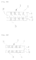
- Fig. 4A is a sectional view of an electric resistance gradient of the single crystal silicon according to the present invention after diffusion
- Fig. 4B is a sectional view of an electric resistance gradient of the single crystal silicon according to the present invention after ion implantation
- FIG. 5A is a sectional view of an electric resistance layer of the single crystal silicon according to the present invention, which depends on a thickness, after diffusion
- Fig. 5B is a sectional view of an electric resistance layer of the single crystal silicon according to the present invention, which depends on a thickness, after ion implantation
- Fig. 6A is a sectional view illustrating formation of pores in a surface part of silicon according to the present invention after diffusion due to anodizing
- Fig. 6B is a sectional view illustrating formation of pores in the surface part of silicon according to the present invention after ion implantation due to anodizing
- Fig. 7A is a sectional view illustrating formation of pores in a middle part of silicon according to the present invention after diffusion due to anodizing
- Fig. 7B is a sectional view illustrating formation of pores in the middle part of silicon according to the present invention after ion implantation due to anodizing.
- the vertical-alignment type porous silicon according to the present invention includes a first pore 11 which is formed in an upper side of the silicon, a second pore 12 which is formed in a lower side of the first pore 11 and has a diameter that is larger or smaller than a diameter of the first pore 11, a third pore 13 which is formed in a lower side of the second pore 12 and has a diameter that is identical or similar to the diameter of the first pore 11, and one or more pore parts 11, 12, and 13 which includes the first pore 11, the second pore 12, and the third pore 13.
- the typical single crystal silicon 2 has the surface on which an oxide film 4 is formed. Since the oxide film 4 may obstruct anodizing of the silicon 2, as shown in Fig. 2 , the oxide film 4 may be removed by using the etching process before the porous silicon 2 according to the present invention is prepared.
- the concentration gradient is formed so that the concentration of the impurity is lowest at the middle part 8 of the silicon and increases as moving toward the surface parts 6 and 10 of the silicon, for example, the upper part 6 and the lower part 10 of the silicon.
- the concentration gradient is formed so that the concentration of the impurity is highest at the middle part 8 of the silicon and decreases as moving toward the surface parts 6 and 10 of the silicon.
- a horizontal direction of Figs. 3A and 3B means the concentration of the impurity and increases as moving toward the right.
- a vertical direction means the thickness of the silicon 2.
- the resistance gradient is formed so that the resistance is highest at the middle part 8 of the silicon and decreases as moving toward the surface parts 6 and 10 of the silicon.
- the resistance gradient is formed so that the resistance is lowest at the middle part 8 of the silicon and increases as moving toward the surface parts 6 and 10 of the silicon.
- the ion implantation means that ionized atoms are accelerated by using energy of tens to hundreds kV to be forcibly implanted into the silicon 2 so that the composition, the combination state, and the crystal structure of the material at the surface of the silicon 2 are changed to improve hardness, wear resistance, corrosion resistance, and fatigue resistance.
- the diffusion means a process in which a material moves from a high concentration region to a low concentration region due to random movement of molecules.
- the silicon 2 is heated at about 1000°C and exposed to gas, thus performing the diffusion.
- the gas may contain any element of Group III or Group V of the periodic table of elements.
- the gas containing boron is used.
- the silicon 2 Due to the above-mentioned resistance gradient, the silicon 2 has three different layers, for example, the upper part 6 of the silicon, the middle part 8 of the silicon, and the lower part 10 of the silicon, according to the thickness direction of the silicon. If the silicon 2 is obtained by using the diffusion, as shown in Fig. 5A , the high resistance layer 14 is formed at the middle part 8 of the silicon, and if the silicon 2 is obtained by using the ion implantation, as shown in Fig. 5B , the high resistance layer 14 is formed at the surface parts 6 and 10 of the silicon.
- the silicon 2 into which the impurity is implanted by using the diffusion is dipped in the solution which contains fluorine or a hydrofluoric acid, for example, the solution which contains 20 % by weight of the hydrofluoric acid (HF) and 80 % by weight of dimethylformamide (DMF), to perform the anodizing, as shown in Figs. 6A and 7A , the first pore 11 and the third pore 13 are formed at the surface parts 6 and 10 of the silicon at which the electric resistance value is low, and the second pore 12 that is larger than the pores 11 and 13 formed in the surface parts 6 and 10 of the silicon is then formed at the middle part 8 of the silicon at which the electric resistance value is high.
- the solution which contains fluorine or a hydrofluoric acid for example, the solution which contains 20 % by weight of the hydrofluoric acid (HF) and 80 % by weight of dimethylformamide (DMF)
- the silicon 2 into which the impurity is implanted by using the ion implantation is dipped in the solution which contains fluorine or the hydrofluoric acid to perform the anodizing, as shown in Figs. 6B and 7B , the first pore 11 and the third pore 13 are formed at the surface parts 6 and 10 of the silicon at which the electric resistance value is high, and the second pore 12 that is smaller than the pores 11 and 13 formed in the surface parts 6 and 10 of the silicon is then formed at the middle part 8 of the silicon at which the electric resistance value is low.
- step parts 16, 16', 18, and 18' are formed between the first pore 11 and the third pore 13, and the second pore 12.
- the step parts 16, 16', 18, and 18' include first step parts 16 and 16' which are vertically symmetrical in the same pore based on a transversal axis direction of the silicon, and second step parts 18 and 18' which are horizontally symmetrical in respects to the first step parts 16 and 16' in the same pore based on a longitudinal axis direction of the silicon.
- a pore part having a double structure is formed in a silicon.
- the silicon having an improved surface area can be obtained as compared to a known porous silicon, and since different electronic materials can be implanted into different pores, it is easy to form interfaces of the implanted electronic materials.
Landscapes
- Chemical & Material Sciences (AREA)
- Engineering & Computer Science (AREA)
- Chemical Kinetics & Catalysis (AREA)
- Electrochemistry (AREA)
- Materials Engineering (AREA)
- Metallurgy (AREA)
- Organic Chemistry (AREA)
- Pressure Sensors (AREA)
- Weting (AREA)
- Porous Artificial Stone Or Porous Ceramic Products (AREA)
- Silicon Compounds (AREA)
Abstract
Description
- The present invention relates to a porous silicon having a step and a method of preparing the same and, more particularly, to a vertical-alignment type porous silicon and a method of preparing the same which includes performing diffusion or ion implantation in respects to a silicon and forming pores having steps by using anodizing.
- A porous silicon has a peculiar structure and an excellent volume ratio and surface area. For this reason, preparation of the porous silicon and development of novel technology using the same come into the spotlight.
- Furthermore, in recent years, light emitting devices, diodes, high performance sensors, thin film electrodes, integrated circuits, and fuel cells have been developed and studied by using the porous silicon in several spaces. In views of studies of characteristics of the porous silicon, the above-mentioned studies relate to a method of using physical properties of the porous silicon, a method of using a surface area, and a method of using electric properties.
- For example,
Korean Patent No. 0392152 - In addition,
Korean Unexamined Patent Application Publication No. 10-1998-032008 - The porous silicon may be prepared by electrochemically anodizing a single crystal silicon while the single crystal silicon is dipped in a hydrofluoric acid (HF) solution. Accordingly, the main factor in the preparation of the porous silicon is electric resistance and a current density of the silicon. However, in practice, various variables other than the electric resistance and the current density affect a pore size and structure of the porous silicon. With respect to this, the mechanism regarding affection of the variables on formation of pores is not known.
- Therefore, the size of the pore which is formed during the preparation of the porous silicon is experimentally obtained for the most case. Accordingly, there are problems in that the porous silicon which is formed by using a known method has frequently an undesired pore shape and an alignment state is poor.
- Additionally, there is a problem in that unnecessary processes such as epitaxial growth or a sealing process are added during the preparation and application of the porous silicon.
- The unnecessary processes cause a waste of resources and energy, and enable unnecessary layers to be formed in addition to the desired porous layer.
- The present invention has been made keeping in mind the above disadvantages occurring in the related arts, an object of the present invention is to provide a vertical-alignment type porous silicon and a method of preparing the same which includes implanting an impurity on a silicon, dipping the silicon in an electrolyte solution, and performing anodizing to change electric resistance of the silicon, so that a diameter of each of pores is controlled or pores having different diameters depending on a thickness direction of the silicon are aligned.
-
-
Fig. 1 is a sectional view of a known single crystal silicon on which an oxide film is formed; -
Fig. 2 is a sectional view of a single crystal silicon from which an oxide film is removed according to the present invention; -
Fig. 3A is a sectional view of an impurity concentration gradient of the single crystal silicon according to the present invention after diffusion; -
Fig. 3B is a sectional view of an impurity concentration gradient of the single crystal silicon according to the present invention after ion implantation; -
Fig. 4A is a sectional view of an electric resistance gradient of the single crystal silicon according to the present invention after diffusion; -
Fig. 4B is a sectional view of an electric resistance gradient of the single crystal silicon according to the present invention after ion implantation; -
Fig. 5A is a sectional view of an electric resistance layer of the single crystal silicon according to the present invention, which depends on a thickness, after diffusion; -
Fig. 5B is a sectional view of an electric resistance layer of the single crystal silicon according to the present invention, which depends on a thickness, after ion implantation; -
Fig. 6A is a sectional view illustrating formation of pores in a surface part of silicon according to the present invention after diffusion due to anodizing; -
Fig. 6B is a sectional view illustrating formation of pores in the surface part of silicon according to the present invention after ion implantation due to anodizing; -
Fig. 7A is a sectional view illustrating formation of pores in a middle part of silicon according to the present invention after diffusion due to anodizing; and -
Fig. 7B is a sectional view illustrating formation of pores in the middle part of silicon according to the present invention after ion implantation due to anodizing. - An aspect of the present invention provides a vertical-alignment type porous silicon including a first pore which is formed in an upper side of the silicon, a second pore which is formed in a lower side of the first pore and has a diameter that is larger or smaller than a diameter of the first pore, a third pore which is formed in a lower side of the second pore and has a diameter that is identical or similar to the diameter of the first pore, and one or more pore parts which includes the first pore, the second pore, and the third pore.
- Another aspect of the present invention provides a method of preparing a vertical-alignment type porous silicon. The method includes (i) implanting an impurity on a silicon, (ii) anodizing the silicon into which the impurity is implanted by using an electrolyte solution to form pores in the silicon, and (iii) drying the silicon in which the pores are formed.
- The first pore according to the present invention is formed in the upper part of the silicon. The first pore is formed through the upper side of the silicon, and may have any shape. It is preferable that the first pore have a hexagonal prism shape or a cylinder shape.
- The second pore according to the present invention is formed in the middle part of the silicon. The second pore is formed through the lower side of the first pore and has a diameter that is larger or smaller than that of the first pore. The second pore may have any shape. It is preferable that the second pore have a hexagonal prism shape or a cylinder shape.
- The third pore according to the present invention is formed in the lower part of the silicon. The third pore is formed through the lower side of the second pore and has a diameter that is identical or similar to that of the first pore. The third pore may have any shape. It is preferable that the third pore have a hexagonal prism shape or a cylinder shape.
- The pore part which includes the first, the second, and the third pores has a surface area that is larger than that of a known vertical-alignment type porous silicon. Since different electronic materials, for example, platinum or Nafion, which are implanted into the pore part can be implanted into the different pores, it is easy to form interfaces of the implanted electronic materials.
- A resistance gradient is formed in the silicon according to the type of impurity which is implanted into the silicon, and the diameter of the pore is controlled in respects to the thickness direction of the silicon according to the resistance gradient. Accordingly, the large pores are formed at an end of the silicon at which a high resistance layer is formed, and the small pores are formed at another end of the silicon at which a low resistance layer is formed.
- The electrolyte solution according to the present invention functions to enable a current to easily flow through the silicon into which the impurity is implanted, so that the silicon is anodized. Any electrolyte solution may be used as long as the electrolyte solution has the above-mentioned function.
- In connection with this, the electrolyte solution may contain fluorine or a hydrofluoric acid.
- The solution which contains fluorine may be a solution containing ammonium fluoride, and the solution which contains the hydrofluoric acid may be a solution containing only the hydrofluoric acid or the hydrofluoric acid and dimethylformamide.
- A method of preparing a vertical-alignment type porous silicon having the above-mentioned configuration according to the present invention includes (i) implanting an impurity on a silicon, (ii) anodizing the silicon into which the impurity is implanted by using an electrolyte solution to form pores in the silicon, and (iii) drying the silicon in which the pores are formed.
- In step i according to the present invention, the impurity is implanted into the silicon. If the impurity is implanted into the silicon, a concentration gradient of the impurity is formed according to the thickness direction of the silicon. In connection with this, the implantation of the impurity may be performed by using ion implantation or diffusion.
- The implantation of the impurity is performed at normal temperature by using the ion implantation, and at a temperature in the range of 900 to 1200°C by using the diffusion.
- In the case of when the impurity is implanted by using the diffusion, the concentration of the impurity is lowest at the middle part of the silicon and increases as moving toward the surface of the silicon, for example, the upper or lower part of the silicon. In the case of when the impurity is implanted by using the ion implantation, the concentration of the impurity is lowest at the surface of the silicon, for example, the upper or lower part of the silicon, and increases as moving toward the middle part of the silicon. Therefore, if the diffusion is used, the resistance gradient is formed so that the resistance is highest at the middle part of the silicon and decreases as moving toward the surface. If the ion implantation is used, the resistance gradient is formed so that the resistance is lowest at the middle part of the silicon and increases as moving toward the surface of the silicon.
- In connection with this, any element of Group III and Group V of the periodic table of elements may be used as the ionized atom which is used to perform the ion implantation. However, it is preferable to use a boron (B) atom.
- In respects to the impurity which is used when the impurity is implanted by using the diffusion, any impurity may be used as long as the impurity can form a resistance gradient on the silicon by using the diffusion. However, it is preferable to use boron or gas containing a Group III or Group V element including boron.
- Due to the above-mentioned resistance gradient, the silicon includes about three different layers according to the thickness direction of the silicon. If the diffusion is performed, the high resistance layer is formed at the middle part of the silicon, and if the ion implantation is performed, the high resistance layer is formed at the surface part of the silicon. In connection with this, the electric resistance layer is confirmed by observing electric resistance while an apparent boundary layer is not observed.
- Meanwhile, since a typical single crystal silicon which is used as the silicon has a surface on which an oxide film is formed, a silicon etching step may be performed to remove the oxide film from the surface of the silicon before step i where the impurity is implanted into the silicon is performed.
- The electric resistance of the silicon from which the oxide film is removed during the etching step depends on the type of silicon, and is constant through the silicon as long as an additional special process is not performed.
- In step ii according to the present invention, the silicon into which the impurity is implanted during step i is anodized by using the electrolyte solution to form the pores in the silicon. A current is applied to the electrolyte solution to anodize the silicon. As a result, the pores are formed. In connection with this, the current density may be in the range of 0.1 to 50 mA/cm2.
- In connection with this, the electrolyte solution may be a solution containing fluorine or a hydrofluoric acid.
- The solution which contains the hydrofluoric acid may be a solution containing only the hydrofluoric acid or 10 to 90 % by weight of the hydrofluoric acid and 10 to 90 % by weight of dimethylformamide (DMF). It is preferable to use a solution which contains 20 % by weight of the hydrofluoric acid and 80 % by weight of dimethylformamide. The solution containing the hydrofluoric acid may further contain acetonitrile if necessary.
- Since the silicon has different resistance values according to the upper part, the middle part, and the lower part thereof, the diameter of the pore which is formed by using the anodizing may depend on the upper part, the middle part, and the lower part of the silicon.
- However, since the electric resistance values of the upper part and the lower part of the silicon are identical or similar to each other, the diameters of the pores which are formed in the upper part and the lower part of the silicon are identical or similar to each other.
- In step iii according to the present invention, the silicon in which the pores are formed during step ii where the silicon is anodized is dried. The silicon is dried at a temperature in the range of 0 to 50°C for 30 to 60 min.
- A washing step of washing the silicon by using water or alcohol may be further performed between the step for anodizing the silicon and the step for drying the silicon in order to remove the residual solvent from the silicon, if necessary.
- In the vertical-alignment type porous silicon which is produced by using the above-mentioned method, since the pores having the different diameters are formed in the silicon to form the pore part having a double structure, the silicon may have an improved surface area as compared to a known porous silicon and it is easy to form boundary layers of contact materials.
- Additionally, since stereoscopic electric properties are ensured, the silicon can have a function required in improved electronic devices. Due to a surface difference and a difference in porosity which are caused by a difference in diameter of the pores according to the thickness direction, the silicon can be usefully applied to fuel cells and improve a sensing ability of a sensor.
- Furthermore, in the case of when the silicon is applied to a mold for manufacturing nanowires, it is possible to manufacture nanowires having a double structure. If the pore of the porous silicon has a double structure, since optical properties depend on the thickness, displaying abilities of light emitting devices and light emitting diodes can be improved.
- The vertical-alignment type porous silicon according to the present invention may be used in light emitting devices, diodes, high-performance sensors, thin film electrodes, integrated circuits, fuel cells and the like.
- In the vertical-alignment type porous silicon according to an aspect of the present invention, platinum (Pt) is provided in the pores formed in the middle part of the silicon and Nafion is implanted in the upper part and the lower part of the silicon to manufacture a fuel cell, thus, the better effect is ensured as compared to a known silicon substrate or porous silicon.
- According to the vertical-alignment type porous silicon of the present invention and a method of preparing the same, compounds of element of Group IV or aluminum may be used instead of silicon to produce a porous electronic material having pore parts if necessary.
- Hereinafter, the present invention will be described in detail with reference to the accompanying drawings. However, the following description is set forth to illustrate, but are not to be construed to limit the present invention.
-
Fig. 2 is a sectional view of a single crystal silicon from which an oxide film is removed according to the present invention,Fig. 3A is a sectional view of an impurity concentration gradient of the single crystal silicon according to the present invention after diffusion,Fig. 3B is a sectional view of an impurity concentration gradient of the single crystal silicon according to the present invention after ion implantation,Fig. 4A is a sectional view of an electric resistance gradient of the single crystal silicon according to the present invention after diffusion,Fig. 4B is a sectional view of an electric resistance gradient of the single crystal silicon according to the present invention after ion implantation,Fig. 5A is a sectional view of an electric resistance layer of the single crystal silicon according to the present invention, which depends on a thickness, after diffusion,Fig. 5B is a sectional view of an electric resistance layer of the single crystal silicon according to the present invention, which depends on a thickness, after ion implantation,Fig. 6A is a sectional view illustrating formation of pores in a surface part of silicon according to the present invention after diffusion due to anodizing,Fig. 6B is a sectional view illustrating formation of pores in the surface part of silicon according to the present invention after ion implantation due to anodizing,Fig. 7A is a sectional view illustrating formation of pores in a middle part of silicon according to the present invention after diffusion due to anodizing, andFig. 7B is a sectional view illustrating formation of pores in the middle part of silicon according to the present invention after ion implantation due to anodizing. - As shown in
Figs. 2 to 7 , the vertical-alignment type porous silicon according to the present invention includes a first pore 11 which is formed in an upper side of the silicon, asecond pore 12 which is formed in a lower side of the first pore 11 and has a diameter that is larger or smaller than a diameter of the first pore 11, athird pore 13 which is formed in a lower side of thesecond pore 12 and has a diameter that is identical or similar to the diameter of the first pore 11, and one ormore pore parts second pore 12, and thethird pore 13. - As shown in
Fig. 1 , the typicalsingle crystal silicon 2 has the surface on which an oxide film 4 is formed. Since the oxide film 4 may obstruct anodizing of thesilicon 2, as shown inFig. 2 , the oxide film 4 may be removed by using the etching process before theporous silicon 2 according to the present invention is prepared. - In respects to the
silicon 2 according to the present invention, in the case of when the impurity is implanted by using the diffusion, as shown inFig. 3A , the concentration gradient is formed so that the concentration of the impurity is lowest at themiddle part 8 of the silicon and increases as moving toward thesurface parts upper part 6 and thelower part 10 of the silicon. In the case of when the impurity is implanted by using the ion implantation, as shown inFig. 3B , the concentration gradient is formed so that the concentration of the impurity is highest at themiddle part 8 of the silicon and decreases as moving toward thesurface parts Figs. 3A and 3B means the concentration of the impurity and increases as moving toward the right. A vertical direction means the thickness of thesilicon 2. - Therefore, in the case of the
silicon 2 which is obtained by using the diffusion, as shown inFig. 4A , the resistance gradient is formed so that the resistance is highest at themiddle part 8 of the silicon and decreases as moving toward thesurface parts silicon 2 which is obtained by using the ion implantation, as shown inFig. 4B , the resistance gradient is formed so that the resistance is lowest at themiddle part 8 of the silicon and increases as moving toward thesurface parts - The ion implantation means that ionized atoms are accelerated by using energy of tens to hundreds kV to be forcibly implanted into the
silicon 2 so that the composition, the combination state, and the crystal structure of the material at the surface of thesilicon 2 are changed to improve hardness, wear resistance, corrosion resistance, and fatigue resistance. - In addition, the diffusion means a process in which a material moves from a high concentration region to a low concentration region due to random movement of molecules. In the present invention, the
silicon 2 is heated at about 1000°C and exposed to gas, thus performing the diffusion. - In connection with this, the gas may contain any element of Group III or Group V of the periodic table of elements. Preferably, the gas containing boron is used.
- Due to the above-mentioned resistance gradient, the
silicon 2 has three different layers, for example, theupper part 6 of the silicon, themiddle part 8 of the silicon, and thelower part 10 of the silicon, according to the thickness direction of the silicon. If thesilicon 2 is obtained by using the diffusion, as shown inFig. 5A , thehigh resistance layer 14 is formed at themiddle part 8 of the silicon, and if thesilicon 2 is obtained by using the ion implantation, as shown inFig. 5B , thehigh resistance layer 14 is formed at thesurface parts - When the
silicon 2 into which the impurity is implanted by using the diffusion is dipped in the solution which contains fluorine or a hydrofluoric acid, for example, the solution which contains 20 % by weight of the hydrofluoric acid (HF) and 80 % by weight of dimethylformamide (DMF), to perform the anodizing, as shown inFigs. 6A and7A , the first pore 11 and thethird pore 13 are formed at thesurface parts second pore 12 that is larger than thepores 11 and 13 formed in thesurface parts middle part 8 of the silicon at which the electric resistance value is high. - In addition, when the
silicon 2 into which the impurity is implanted by using the ion implantation is dipped in the solution which contains fluorine or the hydrofluoric acid to perform the anodizing, as shown inFigs. 6B and7B , the first pore 11 and thethird pore 13 are formed at thesurface parts second pore 12 that is smaller than thepores 11 and 13 formed in thesurface parts middle part 8 of the silicon at which the electric resistance value is low. - Since the
pores surface parts middle part 8 of the silicon,step parts third pore 13, and thesecond pore 12. Thestep parts first step parts 16 and 16' which are vertically symmetrical in the same pore based on a transversal axis direction of the silicon, andsecond step parts 18 and 18' which are horizontally symmetrical in respects to thefirst step parts 16 and 16' in the same pore based on a longitudinal axis direction of the silicon. - The present invention has been described in an illustrative manner, and it is to be understood that the terminology used is intended to be in the nature of description rather than of limitation. Many modifications and variations of the present invention are possible in light of the above teachings. Therefore, it is to be understood that within the scope of the appended claims, the invention may be practiced otherwise than as specifically described.
- According to the present invention as described above, a pore part having a double structure is formed in a silicon. Thus, the silicon having an improved surface area can be obtained as compared to a known porous silicon, and since different electronic materials can be implanted into different pores, it is easy to form interfaces of the implanted electronic materials.
Claims (6)
- A vertical-alignment type porous silicon, comprising:a first pore (11) which is formed in an upper side of the silicon (2);a second pore (12) which is formed in a lower side of the first pore (11) and has a diameter that is larger or smaller than a diameter of the first pore (11);a third pore (13) which is formed in a lower side of the second pore (12) and has a diameter that is identical or similar to the diameter of the first pore (11); andone or more pore parts (11, 12, and 13) which includes the first pore (11), the second pore (12), and the third pore (13).
- The vertical-alignment type porous silicon (2) according to claim 1, characterized in that a step part is formed between the first pore (11) and the third pore (13), and the second pore (12).
- A method of preparing a vertical-alignment type porous silicon, comprising:(i) implanting an impurity on a silicon (2);(ii) anodizing the silicon (2) into which the impurity is implanted by using an electrolyte solution to form pores in the silicon (2); and(iii) drying the silicon (2) in which the pores are formed.
- The method of preparing a vertical-alignment type porous silicon according to claim 3, characterized in that the implanting of the impurity is performed by using ion implantation or diffusion.
- The method of preparing a vertical-alignment type porous silicon according to claim 3, characterized in that the electrolyte solution is formed of a solution containing fluorine or a hydrofluoric acid.
- The method of preparing a vertical-alignment type porous silicon according to claim 5, characterized in that the solution containing the hydrofluoric acid contains 10 to 90 % by weight of hydrofluoric acid and 10 to 90 % by weight of dimethylformamide.
Applications Claiming Priority (1)
| Application Number | Priority Date | Filing Date | Title |
|---|---|---|---|
| KR1020070002121A KR100839376B1 (en) | 2007-01-08 | 2007-01-08 | Porous silicon and its manufacturing method |
Publications (2)
| Publication Number | Publication Date |
|---|---|
| EP1942520A2 true EP1942520A2 (en) | 2008-07-09 |
| EP1942520A3 EP1942520A3 (en) | 2009-11-11 |
Family
ID=39156428
Family Applications (1)
| Application Number | Title | Priority Date | Filing Date |
|---|---|---|---|
| EP20070123736 Withdrawn EP1942520A3 (en) | 2007-01-08 | 2007-12-19 | Porous silicon and method of preparing the same |
Country Status (4)
| Country | Link |
|---|---|
| US (1) | US7972687B2 (en) |
| EP (1) | EP1942520A3 (en) |
| JP (1) | JP4637920B2 (en) |
| KR (1) | KR100839376B1 (en) |
Cited By (2)
| Publication number | Priority date | Publication date | Assignee | Title |
|---|---|---|---|---|
| US9647263B2 (en) | 2010-09-03 | 2017-05-09 | Nexeon Limited | Electroactive material |
| US9871248B2 (en) | 2010-09-03 | 2018-01-16 | Nexeon Limited | Porous electroactive material |
Families Citing this family (1)
| Publication number | Priority date | Publication date | Assignee | Title |
|---|---|---|---|---|
| CN102211770B (en) * | 2010-04-12 | 2012-11-28 | 中国科学院过程工程研究所 | Method for preparing porous silicon material by using catalytic reaction of silicon and halogenated hydrocarbon |
Citations (2)
| Publication number | Priority date | Publication date | Assignee | Title |
|---|---|---|---|---|
| KR19980032008A (en) | 1996-10-09 | 1998-07-25 | 손욱 | Porous silicon, a method of manufacturing the same, and an electroluminescent device using the porous silicon |
| KR100392152B1 (en) | 1993-12-06 | 2003-07-23 | 더 쎄크리터리 오브 스테이트 포 디펜스 인 허 브리태닉 매저스티즈 거번먼트 오브 디 유나이티드 킹덤 오브 그레이트 브리튼 앤드 노던 아일랜드 | Methods of producing porous semiconductor materials and porous silicon produced therefrom |
Family Cites Families (10)
| Publication number | Priority date | Publication date | Assignee | Title |
|---|---|---|---|---|
| JP3171903B2 (en) * | 1992-01-30 | 2001-06-04 | キヤノン株式会社 | Semiconductor substrate and manufacturing method thereof |
| EP0733269B1 (en) | 1993-12-06 | 2002-01-16 | QinetiQ Limited | Porous semiconductor material |
| JP3027092B2 (en) * | 1994-07-27 | 2000-03-27 | シャープ株式会社 | Method of forming porous silicon light emitting layer |
| GB2299204A (en) * | 1995-03-20 | 1996-09-25 | Secr Defence | Electroluminescent device |
| CA2233115C (en) * | 1997-03-27 | 2002-03-12 | Canon Kabushiki Kaisha | Semiconductor substrate and method of manufacturing the same |
| EP1063688A1 (en) * | 1999-01-13 | 2000-12-27 | Mitsubishi Denki Kabushiki Kaisha | Method of producing silicon device |
| JP4027218B2 (en) * | 2002-12-13 | 2007-12-26 | キヤノン株式会社 | Filtration membrane manufacturing method |
| EP1679735B1 (en) * | 2003-10-27 | 2010-06-02 | Panasonic Electric Works Co., Ltd. | Infrared light emitting device and gas sensor using same |
| JP2005183845A (en) * | 2003-12-22 | 2005-07-07 | Canon Inc | Member having porous silicon region and method for producing member containing silicon |
| US20060234391A1 (en) * | 2005-02-18 | 2006-10-19 | University Of Rochester | Optical sensor based on resonant porous silicon structures |
-
2007
- 2007-01-08 KR KR1020070002121A patent/KR100839376B1/en not_active Expired - Fee Related
- 2007-12-19 EP EP20070123736 patent/EP1942520A3/en not_active Withdrawn
- 2007-12-29 US US11/967,138 patent/US7972687B2/en active Active
-
2008
- 2008-01-08 JP JP2008001385A patent/JP4637920B2/en not_active Expired - Fee Related
Patent Citations (2)
| Publication number | Priority date | Publication date | Assignee | Title |
|---|---|---|---|---|
| KR100392152B1 (en) | 1993-12-06 | 2003-07-23 | 더 쎄크리터리 오브 스테이트 포 디펜스 인 허 브리태닉 매저스티즈 거번먼트 오브 디 유나이티드 킹덤 오브 그레이트 브리튼 앤드 노던 아일랜드 | Methods of producing porous semiconductor materials and porous silicon produced therefrom |
| KR19980032008A (en) | 1996-10-09 | 1998-07-25 | 손욱 | Porous silicon, a method of manufacturing the same, and an electroluminescent device using the porous silicon |
Cited By (3)
| Publication number | Priority date | Publication date | Assignee | Title |
|---|---|---|---|---|
| US9647263B2 (en) | 2010-09-03 | 2017-05-09 | Nexeon Limited | Electroactive material |
| US9871248B2 (en) | 2010-09-03 | 2018-01-16 | Nexeon Limited | Porous electroactive material |
| US9947920B2 (en) | 2010-09-03 | 2018-04-17 | Nexeon Limited | Electroactive material |
Also Published As
| Publication number | Publication date |
|---|---|
| US20080166538A1 (en) | 2008-07-10 |
| KR100839376B1 (en) | 2008-06-19 |
| JP2008169484A (en) | 2008-07-24 |
| EP1942520A3 (en) | 2009-11-11 |
| JP4637920B2 (en) | 2011-02-23 |
| US7972687B2 (en) | 2011-07-05 |
Similar Documents
| Publication | Publication Date | Title |
|---|---|---|
| Yan et al. | An ultrathin and highly porous silica nanochannel membrane: toward highly efficient salinity energy conversion | |
| Abd-Elnaiem et al. | Parametric study on the anodization of pure aluminum thin film used in fabricating nano-pores template | |
| Abd-Elnaiem et al. | Effect of the anodization parameters on the volume expansion of anodized aluminum films | |
| Zhang et al. | Simulation of anodizing current-time curves and morphology evolution of TiO2 nanotubes anodized in electrolytes with different NH4F concentrations | |
| Zhong et al. | Fabrication and formation mechanism of triple-layered TiO2 nanotubes | |
| CN102874746A (en) | Method capable of improving uniformity of porous silicon film physical micro-structure and optical characteristics | |
| KR20160146391A (en) | Ionic diode membrane comprising tapered nanopore and method for preparing thereof | |
| Harraz et al. | Cylindrical pore arrays in silicon with intermediate nano-sizes: a template for nanofabrication and multilayer applications | |
| Leitgeb et al. | A combination of metal assisted photochemical and photoelectrochemical etching for tailored porosification of 4H SiC substrates | |
| US7972687B2 (en) | Porous silicon and method of preparing the same | |
| Zhao et al. | The formation mechanism of gradient porous Si in a contactless electrochemical process | |
| US20140255682A1 (en) | Nanoengineered superhydrophobic anti-corrosive aluminum surfaces | |
| CN106531626A (en) | Novel method for improving uniformity of porous silicon radial physical microstructure | |
| Hamm et al. | Silicon anodization in HF ethanoic solutions: competition between pore formation and homogeneous dissolution | |
| Zheng et al. | Thick macroporous membranes made of p‐type silicon | |
| Zhao et al. | Synthesis of porous silicon through interfacial reactions and measurement of its electrochemical response using cyclic voltammetry | |
| Abramova et al. | Nanopore formation during electrolytic etching of silicon in hydrofluoric acid solutions | |
| Zahariev et al. | Effect of pore depth on thickening the barrier layer of porous anodic aluminum oxide | |
| Colibaba et al. | Features of nanotemplates manufacturing on the II-VI compound substrates | |
| Burham et al. | Effect of current density on silicon surface in electrochemical etching | |
| Tanaka et al. | In situ measurement of the diameter of nanopores in silicon during anodization in hydrofluoric acid solution | |
| Haldar et al. | Effect of dimethylformamide, current density and resistivity on pore geometry in p-type macroporous silicon | |
| Selvakumar et al. | A parametrical study of porous silicon for volatile organic chemical sensor applications | |
| Gaev et al. | Kinetics of crack formation in porous silicon | |
| Ge et al. | Experimental research on damage and formation limits on porous silicon materials by electrochemical etching method |
Legal Events
| Date | Code | Title | Description |
|---|---|---|---|
| PUAI | Public reference made under article 153(3) epc to a published international application that has entered the european phase |
Free format text: ORIGINAL CODE: 0009012 |
|
| 17P | Request for examination filed |
Effective date: 20071219 |
|
| AK | Designated contracting states |
Kind code of ref document: A2 Designated state(s): AT BE BG CH CY CZ DE DK EE ES FI FR GB GR HU IE IS IT LI LT LU LV MC MT NL PL PT RO SE SI SK TR |
|
| AX | Request for extension of the european patent |
Extension state: AL BA HR MK RS |
|
| PUAL | Search report despatched |
Free format text: ORIGINAL CODE: 0009013 |
|
| AK | Designated contracting states |
Kind code of ref document: A3 Designated state(s): AT BE BG CH CY CZ DE DK EE ES FI FR GB GR HU IE IS IT LI LT LU LV MC MT NL PL PT RO SE SI SK TR |
|
| AX | Request for extension of the european patent |
Extension state: AL BA HR MK RS |
|
| RIN1 | Information on inventor provided before grant (corrected) |
Inventor name: LEE, YOUNG HWAN Inventor name: LIM, SANG WOO |
|
| 17Q | First examination report despatched |
Effective date: 20100127 |
|
| AKX | Designation fees paid |
Designated state(s): DE |
|
| STAA | Information on the status of an ep patent application or granted ep patent |
Free format text: STATUS: THE APPLICATION IS DEEMED TO BE WITHDRAWN |
|
| 18D | Application deemed to be withdrawn |
Effective date: 20140304 |