EP1942516A2 - Plasma display panel and method of manufacturing the same - Google Patents
Plasma display panel and method of manufacturing the same Download PDFInfo
- Publication number
- EP1942516A2 EP1942516A2 EP07255013A EP07255013A EP1942516A2 EP 1942516 A2 EP1942516 A2 EP 1942516A2 EP 07255013 A EP07255013 A EP 07255013A EP 07255013 A EP07255013 A EP 07255013A EP 1942516 A2 EP1942516 A2 EP 1942516A2
- Authority
- EP
- European Patent Office
- Prior art keywords
- electrode
- electrodes
- dielectric
- display panel
- plasma display
- Prior art date
- Legal status (The legal status is an assumption and is not a legal conclusion. Google has not performed a legal analysis and makes no representation as to the accuracy of the status listed.)
- Withdrawn
Links
Images



Classifications
-
- H—ELECTRICITY
- H01—ELECTRIC ELEMENTS
- H01J—ELECTRIC DISCHARGE TUBES OR DISCHARGE LAMPS
- H01J9/00—Apparatus or processes specially adapted for the manufacture, installation, removal, maintenance of electric discharge tubes, discharge lamps, or parts thereof; Recovery of material from discharge tubes or lamps
- H01J9/02—Manufacture of electrodes or electrode systems
-
- H—ELECTRICITY
- H01—ELECTRIC ELEMENTS
- H01J—ELECTRIC DISCHARGE TUBES OR DISCHARGE LAMPS
- H01J11/00—Gas-filled discharge tubes with alternating current induction of the discharge, e.g. alternating current plasma display panels [AC-PDP]; Gas-filled discharge tubes without any main electrode inside the vessel; Gas-filled discharge tubes with at least one main electrode outside the vessel
- H01J11/10—AC-PDPs with at least one main electrode being out of contact with the plasma
- H01J11/12—AC-PDPs with at least one main electrode being out of contact with the plasma with main electrodes provided on both sides of the discharge space
-
- H—ELECTRICITY
- H01—ELECTRIC ELEMENTS
- H01J—ELECTRIC DISCHARGE TUBES OR DISCHARGE LAMPS
- H01J11/00—Gas-filled discharge tubes with alternating current induction of the discharge, e.g. alternating current plasma display panels [AC-PDP]; Gas-filled discharge tubes without any main electrode inside the vessel; Gas-filled discharge tubes with at least one main electrode outside the vessel
- H01J11/20—Constructional details
- H01J11/22—Electrodes, e.g. special shape, material or configuration
-
- H—ELECTRICITY
- H01—ELECTRIC ELEMENTS
- H01J—ELECTRIC DISCHARGE TUBES OR DISCHARGE LAMPS
- H01J11/00—Gas-filled discharge tubes with alternating current induction of the discharge, e.g. alternating current plasma display panels [AC-PDP]; Gas-filled discharge tubes without any main electrode inside the vessel; Gas-filled discharge tubes with at least one main electrode outside the vessel
- H01J11/20—Constructional details
- H01J11/22—Electrodes, e.g. special shape, material or configuration
- H01J11/24—Sustain electrodes or scan electrodes
-
- H—ELECTRICITY
- H01—ELECTRIC ELEMENTS
- H01J—ELECTRIC DISCHARGE TUBES OR DISCHARGE LAMPS
- H01J11/00—Gas-filled discharge tubes with alternating current induction of the discharge, e.g. alternating current plasma display panels [AC-PDP]; Gas-filled discharge tubes without any main electrode inside the vessel; Gas-filled discharge tubes with at least one main electrode outside the vessel
- H01J11/20—Constructional details
- H01J11/34—Vessels, containers or parts thereof, e.g. substrates
-
- H—ELECTRICITY
- H01—ELECTRIC ELEMENTS
- H01J—ELECTRIC DISCHARGE TUBES OR DISCHARGE LAMPS
- H01J11/00—Gas-filled discharge tubes with alternating current induction of the discharge, e.g. alternating current plasma display panels [AC-PDP]; Gas-filled discharge tubes without any main electrode inside the vessel; Gas-filled discharge tubes with at least one main electrode outside the vessel
- H01J11/20—Constructional details
- H01J11/34—Vessels, containers or parts thereof, e.g. substrates
- H01J11/38—Dielectric or insulating layers
-
- H—ELECTRICITY
- H01—ELECTRIC ELEMENTS
- H01J—ELECTRIC DISCHARGE TUBES OR DISCHARGE LAMPS
- H01J11/00—Gas-filled discharge tubes with alternating current induction of the discharge, e.g. alternating current plasma display panels [AC-PDP]; Gas-filled discharge tubes without any main electrode inside the vessel; Gas-filled discharge tubes with at least one main electrode outside the vessel
- H01J11/20—Constructional details
- H01J11/34—Vessels, containers or parts thereof, e.g. substrates
- H01J11/40—Layers for protecting or enhancing the electron emission, e.g. MgO layers
-
- H—ELECTRICITY
- H01—ELECTRIC ELEMENTS
- H01J—ELECTRIC DISCHARGE TUBES OR DISCHARGE LAMPS
- H01J2211/00—Plasma display panels with alternate current induction of the discharge, e.g. AC-PDPs
- H01J2211/20—Constructional details
- H01J2211/22—Electrodes
- H01J2211/24—Sustain electrodes or scan electrodes
- H01J2211/245—Shape, e.g. cross section or pattern
Definitions
- the present invention relates to a plasma display panel and a method of manufacturing the plasma display panel.
- a plasma display panel is a flat panel display device for displaying characters and/or images by allowing a fluorescent material to emit light generated when gas is discharged.
- a plasma display panel As compared with a liquid crystal display (LCD) or a field emission display (FED), a plasma display panel has higher brightness and higher light emitting efficiency, and therefore a plasma display panel has been considered as a display device capable of replacing a cathode ray tube (CRT).
- CTR cathode ray tube
- a plasma display panel can be classified as a direct current (DC) type plasma display panel or an alternating current (AC) type plasma display panel according to the structure of its pixels arranged in the form of a matrix and the type of waves of drive voltages used.
- DC direct current
- AC alternating current
- all electrodes are exposed to a discharge space so that charges can be directly moved between the electrodes.
- AC type plasma display panel one or more electrodes are surrounded by a dielectric so that charges cannot be directly moved between corresponding electrodes.
- a discharge structure of the plasma display panel can be classified into an opposition discharge structure or a surface discharge structure according to the configuration of electrodes for discharging electricity.
- an opposition discharge structure an address discharge for selecting a pixel and a sustain discharge for sustaining the discharge are generated between a scan electrode (the positive pole) and an address electrode (the negative pole).
- an address discharge for selecting a pixel is generated between an address electrode and a scan electrode, which cross each other, and a sustain discharge for sustaining the discharge is generated between the scan electrode and a sustain electrode.
- FIG. 1 is a perspective schematic view of a conventional plasma display panel and FIG. 2 is a cross-sectional schematic view showing a pixel of the plasma display panel of FIG. 1 .
- the plasma display panel of FIGS. 1 and 2 is an electrode surface light emission type.
- a plurality of sustain electrodes 12a and a plurality of scan electrodes 12b covered by a planar dielectric 15 and a planar passivation layer 16 are formed in parallel on an upper substrate 11.
- the sustain electrodes 12a and the scan electrodes 12b include transparent electrodes 13a and 13b formed of indium tin oxide (ITO) and metal electrodes 14a and 14b for increasing conductivity.
- ITO indium tin oxide
- a plurality of address electrodes 22 covered by a dielectric 23 are formed on a lower substrate 21.
- Partition walls 24 are formed on the dielectric 23 between the plurality of address electrodes 22 in parallel to the address electrodes 22 and fluorescent (or phosphorous) layers 25 are formed on both side surfaces of the partition walls 24 and on a surface of the dielectric 23.
- the upper substrate 11 and the lower substrate 21 are adhered to each other so that the sustain electrodes 12a and the address electrodes 22, and the scan electrodes 12b and the address electrodes 22 are perpendicular to each other.
- a gas for forming plasma is sealed in closed discharge spaces 30 formed by the partition walls 24 to constitute a plurality of pixels.
- the transparent electrode, the metal electrode, the dielectric, and the passivation layer are formed by forming individual layers on the upper substrate 11 and the lower substrate 21 and patterning these individual layers. Then, the upper substrate 11 and the lower substrate 21 are assembled. Therefore, the processes for manufacturing the plasma display panel are complex and the manufacturing cost is high due to use of many materials. Further, since the dielectric 15 and the passivation layer 16 are formed on the upper substrate 11 in the discharge spaces 30, the transmission rate of light emitted from the fluorescent layers 25 is reduced, thereby lowering the light emitting efficiency.
- aspects of embodiments of the present invention are directed to a plasma display panel that can simplify its manufacturing process and/or improve its discharge efficiency, and a method of manufacturing the plasma display panel.
- a plasma display panel as set out in Claim 1.
- Preferred features of this aspect are set out in Claims 2 to 9.
- a method of manufacturing a plasma display panel as set out in Claim 10. Preferred features of this aspect are set out in Claim 11 to 17.
- FIG. 1 is a perspective schematic view of a conventional plasma display panel
- FIG. 2 is a cross-sectional schematic view of a portion of the conventional plasma display panel of FIG. 1 ;
- FIG. 3 is a perspective schematic view of a plasma display panel according to an embodiment of the present invention.
- FIG. 4 is a cross-sectional schematic view of a portion of the plasma display panel of FIG. 3 according to an embodiment of the present invention
- FIGS. 5A and 5B are plan schematic views of a sustain electrode and a scan electrode according to an embodiment of the present invention.
- FIGS. 6A, 6B, 6C, and 6D are cross-sectional schematic views for illustrating a method of manufacturing a plasma display panel according to a first embodiment of the present invention.
- FIGS. 7A, 7B, 7C, and 7D are cross-sectional schematic views for illustrating a method of manufacturing a plasma display panel according to a second embodiment of the present invention.
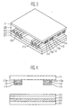
- FIG. 3 is a perspective schematic view of a plasma display panel according to an embodiment of the present invention
- FIG. 4 is a cross-sectional schematic view showing a pixel of the plasma display panel of FIG. 3 .
- a plurality of sustain electrodes 112a and a plurality of scan electrodes 112b are formed in parallel on an upper (or first) substrate 111.
- the sustain electrodes 112a (first electrodes) and the scan electrodes 112b (second electrodes) are surrounded by a dielectric 113.
- the dielectric 113 comprises bridge portions connecting the sustain electrodes 112a (first electrodes) and the scan electrodes 112b (second electrodes).
- a passivation layer 114 is formed on the dielectric 113 surrounding the surfaces of the sustain electrodes 112a and the scan electrodes 112b.
- the dielectric 113 comprises first portions that at least partially surround the sustain electrodes 112a (first electrodes), and second portions that at least partially surround the scan electrodes 112b (second electrodes).
- the passivation layer 114 comprises first portions at least partially surrounding the first portions of the dielectric 113 and second portions at least partially surrounding the second portions of the dielectric 113.
- the combination of the passivation layer 113 surrounding a respective first portion of the dielectric 113 that in turn surrounds a sustain electrode 112a forms a first member that is substantially bar shaped in cross section.
- the combination of a second portion of the passivation layer 114, a second portion of the dielectric 113 surrounding a scan electrode 112b forms a second member that is substantially bar shaped in cross section. In other embodiments, other cross-sectional shapes could be used.
- a plurality of address electrodes 212 are formed on a lower (or second) substrate 211 so as to cross the sustain electrodes 112a and the scan electrodes 112b, and a dielectric 213 is formed on the address electrodes 212.
- Partition walls 214 are formed on the dielectric 213 between the address electrodes 212 in parallel to the address electrodes 212 and fluorescent (or phosphorous) layers 215 are formed on both side surfaces of the partition walls 214 and a surface of the dielectric 213.
- the upper substrate 111 and the lower substrate 211 are adhered to each other so that the sustain electrodes 112a and the address electrodes 212, and the scan electrodes 112b and the address electrodes 212 are perpendicular to each other, thereby forming discharge spaces 220 with the partition walls 214.
- a gas for forming plasma is sealed in the discharge spaces 220 to constitute a plurality of pixels. Inert mixture gases such as He+Xe, Ne+Xe, and He+Xe+Ne can be used as the gas for forming plasma.
- the sustain electrode 112a and the scan electrode 112b are formed of metal sheet(s) 112 such as aluminum sheet(s) of a thickness that may be predetermined and are connected to each other by a bridge 112c of the metal sheet(s) 112.
- the sustain electrode 112a and the scan electrode 112b disposed in parallel at an interval and the bridge 112c connecting the sustain electrode 112a and the scan electrode 112b can be formed by patterning the metal sheet(s) 112 through photographing and etching processes as shown in FIG. 5A .
- the dielectric 113 can be formed to surround the entire surfaces of the sustain electrodes 112a and the scan electrodes 112b or can be formed on remaining surfaces of the sustain electrodes 112a and the scan electrodes 112b except for surfaces opposing the upper substrate 111.
- the dielectric 113 can be formed of an oxide including metal atoms of the sustain electrodes 112a and the scan electrodes 112b. For example, if the metal sheet 112 patterned as shown in FIG. 5A is oxidized to a thickness that may be predetermined, the surfaces of the sustain electrodes 112a and the scan electrodes 112b are oxidized as shown in FIG. 5B and the dielectric 113 including a metal oxide is formed. Then, as shown in FIG.
- the dielectric 113 formed of a metal oxide is formed on the surfaces of the sustain electrode 112a and the scan electrode 112b as shown in FIG. 5B and the bridge is completely changed to an oxide. Therefore, although the sustain electrode 112a and the scan electrode 112b are structurally (or physically) connected to each other by the bridge 112c, the sustain electrode 112a and the scan electrode 112b are electrically insulated (or separated) from each other because the material forming the bridge 112c has been completely changed to an oxide.
- the plasma display panel as described above can be manufactured by the following method.
- FIGS. 6A to 6D are cross-sectional schematic views for illustrating a method of manufacturing the plasma display panel according to a first embodiment of the present invention and FIGS. 5A and 5B will be referred to again.
- the sustain electrode 112a and the scan electrode 112b disposed in parallel at an interval, and the bridge 112c connecting the sustain electrode 112a and the scan electrode 112b are formed by patterning the metal sheet 112.
- the metal sheet 112 is an aluminum sheet of a thickness that may be predetermined.
- FIG. 6A is a cross-sectional view taken along the line A1-A2 of FIG. 5A .
- the sustain electrode 112a, the scan electrode 112b, and the bridge 112c take the form of a sheet and are integrally connected to each other.
- FIGS. 5B and 6B the surfaces of the sustain electrode 112a and the scan electrode 112b are oxidized to a thickness (that may be predetermined) in an oxidation process to form the dielectric 113 including a metal oxide such as Al 2 O 3 . Then, if the oxidation process is performed so as to completely oxidize the bridge 112c, the sustain electrode 112a and the scan electrode 112b are structurally connected to each other but are electrically separated from each other.
- FIG. 6B is a cross-sectional view taken along the line A11-A12 of FIG. 5B .
- the sustain electrode 112a and the scan electrode 112b in the form of a sheet integrally connected by the bridge 112c are bonded to the upper substrate 111 using an adhesive 115.
- the passivation layer 114 is formed on the dielectric 113 using magnesium oxide etc. In one embodiment, the passivation layer 114 is formed on the dielectric 113 and on the sustain and scan electrodes 112a and 112b.
- the sustain electrode 112a and the scan electrode 112b, and the bridge connecting the sustain electrode 112a and the scan electrode 112b are formed by patterning the metal sheet 112. Further, after the dielectric 113 is formed by oxidizing the surfaces of the sustain electrode 112a and the scan electrode 112b connected to each other by the bridge 112c, it is bonded to the upper substrate 111 using an adhesive. In this case, since the dielectric 113 surrounds all the surfaces of the sustain electrode 112a and the scan electrode 112b, the dielectric 113 is interposed between the upper substrate 111 and the sustain electrode 112a and the scan electrode 112b.
- FIGS. 7A to 7D are cross-sectional views for illustrating a plasma display panel formed according to a second preferred embodiment of the present invention.
- a sustain electrode 312a and a scan electrode 312b disposed in parallel at an interval, and a bridge 312c connecting the sustain electrode 312a and the scan electrode 312b are formed by patterning a metal sheet 312.
- the metal sheet 312 is an aluminum sheet of a thickness that may be predetermined.
- the sustain electrode 312a, the scan electrode 312b, and the bridge 312c take the form of a sheet and are integrally connected to each other.
- the sustain electrode 312a and the scan electrode 312b in the form of a sheet integrally connected by the bridge 312c are bonded to an upper substrate 311 using an adhesive 315.
- the surfaces of the sustain electrode 312a and the scan electrode 312b are oxidized to a thickness that may be predetermined in an oxidation process that may be predetermined to form a dielectric 313 including a metal oxide such as Al 2 O 3 . Then, if the oxidation process is performed so as to completely oxidize the bridge 312c, the sustain electrode 312a and the scan electrode 312b are structurally connected to each other but are electrically separated from each other.
- the passivation layer 314 is formed on the dielectric 313 using magnesium oxide (MgO), etc. In one embodiment, the passivation layer 314 is formed on the dielectric 313 and on the sustain and scan electrodes 312a and 312b.
- MgO magnesium oxide
- the scan electrode 312b and the bridge 312c connecting the sustain electrode 312a and the scan electrode 312b are formed by patterning the metal sheet 312, the electrodes are then bonded to the upper substrate 311 using an adhesive. Further, the dielectric 313 including a metal oxide is formed on the surfaces of the sustain electrode 312a and the scan electrode 312b by performing the oxidation process so that the bridge 312c can be completely oxidized.
- the dielectric 313 is formed only on the remaining surfaces of the sustain and scan electrodes 312a and 312b except for surfaces opposing the upper substrate 311, the dielectric is not interposed between the upper substrate 311 and the sustain electrode 312a and the scan electrode 312b.
- an image of a desired gradation is displayed by dividing a unit frame into a plurality of sub-fields and sequentially performing an initialization process, an address process, and a sustain and discharge process in the sub-fields.
- initialization process the address process, and the sustain and discharge process
- drive signals having voltage waves or predetermined voltage waves
- an embodiment of the present invention forms a scan electrode and a sustain electrode connected by a bridge using a metal sheet, in which a dielectric of a metal oxide is formed on the surfaces thereof.
- the scan electrode and the sustain electrode in the form of a sheet are bonded to an upper substrate.
- the discharge voltage Vs can be reduced by increasing the opposing surfaces of the scan electrode and the sustain electrode.
- the light emitting area can be sufficiently increased (or secured) by increasing the distance between the scan electrode and the sustain electrode.
- the transmission rate of light is increased by further exposing a substrate of the discharge space, thereby improving discharge efficiency.
Landscapes
- Engineering & Computer Science (AREA)
- Physics & Mathematics (AREA)
- Plasma & Fusion (AREA)
- Chemical & Material Sciences (AREA)
- Materials Engineering (AREA)
- Manufacturing & Machinery (AREA)
- Gas-Filled Discharge Tubes (AREA)
Abstract
Description
- The present invention relates to a plasma display panel and a method of manufacturing the plasma display panel.
- A plasma display panel (PDP) is a flat panel display device for displaying characters and/or images by allowing a fluorescent material to emit light generated when gas is discharged. As compared with a liquid crystal display (LCD) or a field emission display (FED), a plasma display panel has higher brightness and higher light emitting efficiency, and therefore a plasma display panel has been considered as a display device capable of replacing a cathode ray tube (CRT).
- A plasma display panel can be classified as a direct current (DC) type plasma display panel or an alternating current (AC) type plasma display panel according to the structure of its pixels arranged in the form of a matrix and the type of waves of drive voltages used. In such a DC type plasma display panel, all electrodes are exposed to a discharge space so that charges can be directly moved between the electrodes. In an AC type plasma display panel, one or more electrodes are surrounded by a dielectric so that charges cannot be directly moved between corresponding electrodes.
- Further, a discharge structure of the plasma display panel can be classified into an opposition discharge structure or a surface discharge structure according to the configuration of electrodes for discharging electricity. In an opposition discharge structure, an address discharge for selecting a pixel and a sustain discharge for sustaining the discharge are generated between a scan electrode (the positive pole) and an address electrode (the negative pole). By contrast, in a surface discharge structure, an address discharge for selecting a pixel is generated between an address electrode and a scan electrode, which cross each other, and a sustain discharge for sustaining the discharge is generated between the scan electrode and a sustain electrode.
-
FIG. 1 is a perspective schematic view of a conventional plasma display panel andFIG. 2 is a cross-sectional schematic view showing a pixel of the plasma display panel ofFIG. 1 . The plasma display panel ofFIGS. 1 and 2 is an electrode surface light emission type. - Referring to
FIGS. 1 and 2 , a plurality of sustainelectrodes 12a and a plurality ofscan electrodes 12b covered by a planar dielectric 15 and aplanar passivation layer 16 are formed in parallel on anupper substrate 11. Thesustain electrodes 12a and thescan electrodes 12b includetransparent electrodes metal electrodes - A plurality of
address electrodes 22 covered by a dielectric 23 are formed on alower substrate 21.Partition walls 24 are formed on the dielectric 23 between the plurality ofaddress electrodes 22 in parallel to theaddress electrodes 22 and fluorescent (or phosphorous)layers 25 are formed on both side surfaces of thepartition walls 24 and on a surface of the dielectric 23. - The
upper substrate 11 and thelower substrate 21 are adhered to each other so that thesustain electrodes 12a and theaddress electrodes 22, and thescan electrodes 12b and theaddress electrodes 22 are perpendicular to each other. A gas for forming plasma is sealed in closeddischarge spaces 30 formed by thepartition walls 24 to constitute a plurality of pixels. - As mentioned above, in a conventional plasma display panel, the transparent electrode, the metal electrode, the dielectric, and the passivation layer are formed by forming individual layers on the
upper substrate 11 and thelower substrate 21 and patterning these individual layers. Then, theupper substrate 11 and thelower substrate 21 are assembled. Therefore, the processes for manufacturing the plasma display panel are complex and the manufacturing cost is high due to use of many materials. Further, since the dielectric 15 and thepassivation layer 16 are formed on theupper substrate 11 in thedischarge spaces 30, the transmission rate of light emitted from thefluorescent layers 25 is reduced, thereby lowering the light emitting efficiency. - Aspects of embodiments of the present invention are directed to a plasma display panel that can simplify its manufacturing process and/or improve its discharge efficiency, and a method of manufacturing the plasma display panel.
- According to a first aspect of the present invention there is provided a plasma display panel as set out in Claim 1. Preferred features of this aspect are set out in Claims 2 to 9.
- According to a second aspect of the present invention there is provided a method of manufacturing a plasma display panel as set out in Claim 10. Preferred features of this aspect are set out in
Claim 11 to 17. - The accompanying drawings, together with the specification, illustrate exemplary embodiments of the present invention, and, together with the description, serve to explain the principles of the present invention.
-
FIG. 1 is a perspective schematic view of a conventional plasma display panel; -
FIG. 2 is a cross-sectional schematic view of a portion of the conventional plasma display panel ofFIG. 1 ; -
FIG. 3 is a perspective schematic view of a plasma display panel according to an embodiment of the present invention; -
FIG. 4 is a cross-sectional schematic view of a portion of the plasma display panel ofFIG. 3 according to an embodiment of the present invention; -
FIGS. 5A and 5B are plan schematic views of a sustain electrode and a scan electrode according to an embodiment of the present invention; -
FIGS. 6A, 6B, 6C, and 6D are cross-sectional schematic views for illustrating a method of manufacturing a plasma display panel according to a first embodiment of the present invention; and -
FIGS. 7A, 7B, 7C, and 7D are cross-sectional schematic views for illustrating a method of manufacturing a plasma display panel according to a second embodiment of the present invention. - Hereinafter, exemplary embodiments according to the present invention will be described with reference to the accompanying drawings. Here, when one element is described as being connected to another element, one element may be not only directly connected to another element but instead may be indirectly connected to another element via one or more other elements. Also, in the context of the present application, when an element is referred to as being "on" another element, it can be directly on the another element or be indirectly on the another element with one or more intervening elements interposed therebetween. Further, some of the elements that are not essential to the complete description of the invention have been omitted for clarity. Also, like reference numerals refer to like elements throughout.
-
FIG. 3 is a perspective schematic view of a plasma display panel according to an embodiment of the present invention, andFIG. 4 is a cross-sectional schematic view showing a pixel of the plasma display panel ofFIG. 3 . - Referring to
FIGS. 3 and 4 , a plurality of sustainelectrodes 112a and a plurality ofscan electrodes 112b are formed in parallel on an upper (or first)substrate 111. Thesustain electrodes 112a (first electrodes) and thescan electrodes 112b (second electrodes) are surrounded by a dielectric 113. In some embodiments, the dielectric 113 comprises bridge portions connecting thesustain electrodes 112a (first electrodes) and thescan electrodes 112b (second electrodes). Apassivation layer 114 is formed on the dielectric 113 surrounding the surfaces of thesustain electrodes 112a and thescan electrodes 112b. In other words, the dielectric 113 comprises first portions that at least partially surround thesustain electrodes 112a (first electrodes), and second portions that at least partially surround thescan electrodes 112b (second electrodes). Thepassivation layer 114 comprises first portions at least partially surrounding the first portions of the dielectric 113 and second portions at least partially surrounding the second portions of the dielectric 113. In some embodiments, for eachsustain electrode 112a, the combination of thepassivation layer 113 surrounding a respective first portion of the dielectric 113 that in turn surrounds asustain electrode 112a forms a first member that is substantially bar shaped in cross section. Similarly, in some embodiments, the combination of a second portion of thepassivation layer 114, a second portion of the dielectric 113 surrounding ascan electrode 112b forms a second member that is substantially bar shaped in cross section. In other embodiments, other cross-sectional shapes could be used. - A plurality of
address electrodes 212 are formed on a lower (or second)substrate 211 so as to cross thesustain electrodes 112a and thescan electrodes 112b, and a dielectric 213 is formed on theaddress electrodes 212.Partition walls 214 are formed on the dielectric 213 between theaddress electrodes 212 in parallel to theaddress electrodes 212 and fluorescent (or phosphorous)layers 215 are formed on both side surfaces of thepartition walls 214 and a surface of the dielectric 213. - In one embodiment, the
upper substrate 111 and thelower substrate 211 are adhered to each other so that thesustain electrodes 112a and theaddress electrodes 212, and thescan electrodes 112b and theaddress electrodes 212 are perpendicular to each other, thereby forming discharge spaces 220 with thepartition walls 214. A gas for forming plasma is sealed in the discharge spaces 220 to constitute a plurality of pixels. Inert mixture gases such as He+Xe, Ne+Xe, and He+Xe+Ne can be used as the gas for forming plasma. - As shown in
FIG. 5A , the sustainelectrode 112a and thescan electrode 112b are formed of metal sheet(s) 112 such as aluminum sheet(s) of a thickness that may be predetermined and are connected to each other by abridge 112c of the metal sheet(s) 112. For example, the sustainelectrode 112a and thescan electrode 112b disposed in parallel at an interval and thebridge 112c connecting the sustainelectrode 112a and thescan electrode 112b can be formed by patterning the metal sheet(s) 112 through photographing and etching processes as shown inFIG. 5A . - The dielectric 113 can be formed to surround the entire surfaces of the sustain
electrodes 112a and thescan electrodes 112b or can be formed on remaining surfaces of the sustainelectrodes 112a and thescan electrodes 112b except for surfaces opposing theupper substrate 111. The dielectric 113 can be formed of an oxide including metal atoms of the sustainelectrodes 112a and thescan electrodes 112b. For example, if themetal sheet 112 patterned as shown inFIG. 5A is oxidized to a thickness that may be predetermined, the surfaces of the sustainelectrodes 112a and thescan electrodes 112b are oxidized as shown inFIG. 5B and the dielectric 113 including a metal oxide is formed. Then, as shown inFIG. 5A , if the widths D1 of the sustainelectrode 112a and thescan electrode 112b are larger than the width D2 of thebridge 112c and the oxidation process is performed so as to completely oxidize thebridge 112c, the dielectric 113 formed of a metal oxide is formed on the surfaces of the sustainelectrode 112a and thescan electrode 112b as shown inFIG. 5B and the bridge is completely changed to an oxide. Therefore, although the sustainelectrode 112a and thescan electrode 112b are structurally (or physically) connected to each other by thebridge 112c, the sustainelectrode 112a and thescan electrode 112b are electrically insulated (or separated) from each other because the material forming thebridge 112c has been completely changed to an oxide. - According to an embodiment of the present invention, the plasma display panel as described above can be manufactured by the following method.
-
FIGS. 6A to 6D are cross-sectional schematic views for illustrating a method of manufacturing the plasma display panel according to a first embodiment of the present invention andFIGS. 5A and 5B will be referred to again. - Referring to
FIGS. 5A and6A , the sustainelectrode 112a and thescan electrode 112b disposed in parallel at an interval, and thebridge 112c connecting the sustainelectrode 112a and thescan electrode 112b are formed by patterning themetal sheet 112. In one embodiment, for example, themetal sheet 112 is an aluminum sheet of a thickness that may be predetermined.FIG. 6A is a cross-sectional view taken along the line A1-A2 ofFIG. 5A . The sustainelectrode 112a, thescan electrode 112b, and thebridge 112c take the form of a sheet and are integrally connected to each other. - Referring to
FIGS. 5B and6B , the surfaces of the sustainelectrode 112a and thescan electrode 112b are oxidized to a thickness (that may be predetermined) in an oxidation process to form the dielectric 113 including a metal oxide such as Al2O3. Then, if the oxidation process is performed so as to completely oxidize thebridge 112c, the sustainelectrode 112a and thescan electrode 112b are structurally connected to each other but are electrically separated from each other.FIG. 6B is a cross-sectional view taken along the line A11-A12 ofFIG. 5B . - Referring to
FIG. 6C , the sustainelectrode 112a and thescan electrode 112b in the form of a sheet integrally connected by thebridge 112c are bonded to theupper substrate 111 using an adhesive 115. - Referring to
FIG. 6D , thepassivation layer 114 is formed on the dielectric 113 using magnesium oxide etc. In one embodiment, thepassivation layer 114 is formed on the dielectric 113 and on the sustain and scanelectrodes - As mentioned above, in the first embodiment of the present invention, the sustain
electrode 112a and thescan electrode 112b, and the bridge connecting the sustainelectrode 112a and thescan electrode 112b are formed by patterning themetal sheet 112. Further, after the dielectric 113 is formed by oxidizing the surfaces of the sustainelectrode 112a and thescan electrode 112b connected to each other by thebridge 112c, it is bonded to theupper substrate 111 using an adhesive. In this case, since the dielectric 113 surrounds all the surfaces of the sustainelectrode 112a and thescan electrode 112b, the dielectric 113 is interposed between theupper substrate 111 and the sustainelectrode 112a and thescan electrode 112b. -
FIGS. 7A to 7D are cross-sectional views for illustrating a plasma display panel formed according to a second preferred embodiment of the present invention. - Referring to
FIG. 7A , a sustainelectrode 312a and ascan electrode 312b disposed in parallel at an interval, and abridge 312c connecting the sustainelectrode 312a and thescan electrode 312b are formed by patterning ametal sheet 312. In one embodiment, themetal sheet 312 is an aluminum sheet of a thickness that may be predetermined. The sustainelectrode 312a, thescan electrode 312b, and thebridge 312c take the form of a sheet and are integrally connected to each other. - Referring to
FIG. 7B , the sustainelectrode 312a and thescan electrode 312b in the form of a sheet integrally connected by thebridge 312c are bonded to anupper substrate 311 using an adhesive 315. - Referring to
FIG. 7C , the surfaces of the sustainelectrode 312a and thescan electrode 312b are oxidized to a thickness that may be predetermined in an oxidation process that may be predetermined to form a dielectric 313 including a metal oxide such as Al2O3. Then, if the oxidation process is performed so as to completely oxidize thebridge 312c, the sustainelectrode 312a and thescan electrode 312b are structurally connected to each other but are electrically separated from each other. - Referring to
FIG. 7D , thepassivation layer 314 is formed on the dielectric 313 using magnesium oxide (MgO), etc. In one embodiment, thepassivation layer 314 is formed on the dielectric 313 and on the sustain and scanelectrodes - As mentioned above, in the second embodiment of the present invention, after the sustain
electrode 312a, thescan electrode 312b and thebridge 312c connecting the sustainelectrode 312a and thescan electrode 312b are formed by patterning themetal sheet 312, the electrodes are then bonded to theupper substrate 311 using an adhesive. Further, the dielectric 313 including a metal oxide is formed on the surfaces of the sustainelectrode 312a and thescan electrode 312b by performing the oxidation process so that thebridge 312c can be completely oxidized. In this case, since the dielectric 313 is formed only on the remaining surfaces of the sustain and scanelectrodes upper substrate 311, the dielectric is not interposed between theupper substrate 311 and the sustainelectrode 312a and thescan electrode 312b. - In a plasma display panel according to an embodiment of the present invention, an image of a desired gradation is displayed by dividing a unit frame into a plurality of sub-fields and sequentially performing an initialization process, an address process, and a sustain and discharge process in the sub-fields. In the initialization process, the address process, and the sustain and discharge process, drive signals having voltage waves (or predetermined voltage waves) are applied to the sustain electrode, the scan electrode, and the address electrode.
- As mentioned above, an embodiment of the present invention forms a scan electrode and a sustain electrode connected by a bridge using a metal sheet, in which a dielectric of a metal oxide is formed on the surfaces thereof. Here, the scan electrode and the sustain electrode in the form of a sheet are bonded to an upper substrate.
- According to an embodiment of the present invention, since the number of processes for manufacturing the scan electrode, the sustain electrode, and/or the dielectric is reduced, and the scan electrode and the sustain electrode can be easily assembled; the manufacturing cost can be effectively reduced. Further, in one embodiment, the discharge voltage Vs can be reduced by increasing the opposing surfaces of the scan electrode and the sustain electrode. In addition, the light emitting area can be sufficiently increased (or secured) by increasing the distance between the scan electrode and the sustain electrode. Furthermore, the transmission rate of light is increased by further exposing a substrate of the discharge space, thereby improving discharge efficiency.
- While the present invention has been described in connection with certain exemplary embodiments, it is to be understood that the invention is not limited to the disclosed embodiments, but, on the contrary, is intended to cover various modifications and equivalent arrangements included within the scope of the appended claims, and equivalents thereof.
Claims (17)
- A plasma display panel comprising:a first substrate;a plurality of first electrodes and a plurality of second electrodes, the first and second electrodes being disposed in parallel on the first substrate;a first dielectric comprising first portions at least partially surrounding the first electrodes and second portions at least partially surrounding the second electrodes;a passivation layer comprising first portions at least partially surrounding the first portions of the first dielectric and second portions at least partially surrounding the second portions of the first dielectric;a second substrate facing the first substrate;a plurality of third electrodes on the second substrate and crossing the first electrodes and the second electrodes; anda second dielectric on the third electrodes.
- A plasma display panel according to claim 1, wherein the first dielectric comprises bridge portions connecting the first electrodes and the second electrodes.
- A plasma display panel according to claim 1 or 2, wherein a combination of a first electrode, a respective first portion of the first dielectric that surrounds said first electrode, and a respective first portion of the passivation layer that surrounds said first portion of the first dielectric forms a first member that is substantially bar shaped in cross section.
- A plasma display panel according to any one of claims 1 to 3, wherein a combination of a second electrode, a respective second portion of the first dielectric that surrounds said second electrode, and a respective second portion of the passivation layer that surrounds said second portion of the first dielectric forms a second member that is substantially bar shaped in cross section.
- A plasma display panel according to any one of claims 1 to 4, wherein the first and second electrodes comprise metal and the first dielectric comprises an oxidized substance, the oxidized substance comprising an oxide of the metal of the first electrodes and the second electrodes.
- A plasma display panel according to any one of claim 1 to 5, wherein the first dielectric comprises oxidized portions of the first electrodes and the second electrodes.
- A plasma display panel according to any one of claims 1 to 6, further comprising:an adhesive comprising portions located between the first substrate and the first electrodes and portions located between the first substrate and the second electrodes.
- A plasma display panel according to any one of claims 1 to 7, wherein the first electrodes, the second electrodes, and the first dielectric are formed from a same metal sheet.
- A plasma display panel according to claim 8, wherein the metal sheet comprises aluminum.
- A method of manufacturing a plasma display panel, the method comprising:forming a first electrode, a second electrode, and a bridge connecting the first electrode and the second electrode by patterning a metal sheet;forming a dielectric by oxidizing surfaces of the first electrode and the second electrode to a thickness of the first electrode and the second electrode;bonding the first electrode and the second electrode to a substrate; andforming a passivation layer on the dielectric.
- A method according to claim 10, wherein the metal sheet comprises aluminum.
- A method according to claim 10 or 11, wherein the bridge has a width smaller than that of the first electrode and the second electrode.
- A method according to any one of claims 10 to 12, wherein the forming of the dielectric comprises an oxidation process that completely oxidizes the bridge.
- A method according to any one of claims 10 to 13, wherein the bonding of the first electrode and the second electrode to the substrate comprises using an adhesive to bond the first electrode and the second electrode to the substrate.
- A method according to any one of claims 10 to 14, wherein the forming of the dielectric comprises oxidizing the surfaces of the first electrode and the second electrode to the thickness of the first electrode and the second electrode after the first electrode and the second electrode are bonded to the substrate.
- A method according to any one of claims 10 to 15, wherein the forming of the dielectric comprises oxidizing the surfaces of the first electrode and the second electrode to the thickness of the first electrode and the second electrode before the first electrode and the second electrode are bonded to the substrate.
- A method according to any one of claims 10 to 16, wherein the method comprises forming a plurality of first electrodes and a plurality of second electrodes.
Applications Claiming Priority (1)
| Application Number | Priority Date | Filing Date | Title |
|---|---|---|---|
| KR1020070000366A KR100830326B1 (en) | 2007-01-02 | 2007-01-02 | Plasma Display Panel And Method Of Manufacturing The Same |
Publications (2)
| Publication Number | Publication Date |
|---|---|
| EP1942516A2 true EP1942516A2 (en) | 2008-07-09 |
| EP1942516A3 EP1942516A3 (en) | 2008-08-27 |
Family
ID=39363887
Family Applications (1)
| Application Number | Title | Priority Date | Filing Date |
|---|---|---|---|
| EP07255013A Withdrawn EP1942516A3 (en) | 2007-01-02 | 2007-12-21 | Plasma display panel and method of manufacturing the same |
Country Status (5)
| Country | Link |
|---|---|
| US (1) | US20080158105A1 (en) |
| EP (1) | EP1942516A3 (en) |
| JP (1) | JP2008166242A (en) |
| KR (1) | KR100830326B1 (en) |
| CN (1) | CN101217094A (en) |
Family Cites Families (9)
| Publication number | Priority date | Publication date | Assignee | Title |
|---|---|---|---|---|
| JPH0770289B2 (en) * | 1991-11-29 | 1995-07-31 | 株式会社ティーティーティー | Display discharge tube |
| KR100186540B1 (en) * | 1996-04-25 | 1999-03-20 | 구자홍 | Electrode of pdp and its forming method |
| US6037713A (en) * | 1996-11-25 | 2000-03-14 | Fujitsu Limited | Display panel having compound film covered electrodes |
| JP2001015038A (en) | 1999-06-30 | 2001-01-19 | Fujitsu Ltd | Plasma display panel |
| US6509689B1 (en) * | 2000-05-22 | 2003-01-21 | Plasmion Displays, Llc | Plasma display panel having trench type discharge space and method of fabricating the same |
| JP2002190253A (en) | 2000-12-19 | 2002-07-05 | Gendai Plasma Kk | Ac type plasma display panel having good luminous efficacy |
| US7067979B2 (en) * | 2001-10-02 | 2006-06-27 | Noritake Co., Limited | Gas-discharge display device and its manufacturing method |
| KR100922745B1 (en) * | 2004-04-27 | 2009-10-22 | 삼성에스디아이 주식회사 | Plasma display panel |
| KR100768187B1 (en) * | 2004-10-26 | 2007-10-17 | 삼성에스디아이 주식회사 | Plasma display panel |
-
2007
- 2007-01-02 KR KR1020070000366A patent/KR100830326B1/en not_active Expired - Fee Related
- 2007-02-22 JP JP2007042754A patent/JP2008166242A/en active Pending
- 2007-09-20 US US11/858,833 patent/US20080158105A1/en not_active Abandoned
- 2007-12-21 EP EP07255013A patent/EP1942516A3/en not_active Withdrawn
- 2007-12-28 CN CNA2007103066049A patent/CN101217094A/en active Pending
Also Published As
| Publication number | Publication date |
|---|---|
| EP1942516A3 (en) | 2008-08-27 |
| CN101217094A (en) | 2008-07-09 |
| US20080158105A1 (en) | 2008-07-03 |
| JP2008166242A (en) | 2008-07-17 |
| KR100830326B1 (en) | 2008-05-16 |
Similar Documents
| Publication | Publication Date | Title |
|---|---|---|
| US20020145387A1 (en) | Plasma display panel | |
| US20030042839A1 (en) | AC-type gas discharge display | |
| US6936965B1 (en) | Plasma display panel | |
| US6608447B2 (en) | Plasma display panel and driving method thereof | |
| US6628075B1 (en) | Plasma display panel with first and second inner and outer electrodes | |
| US20060132050A1 (en) | Display device | |
| EP1763052A2 (en) | Plasma Display Panel | |
| US20080158105A1 (en) | Plasma display panel and method of manufacturing the same | |
| CN100543806C (en) | plasma display device | |
| EP1770746A1 (en) | Plasma Display Panel | |
| EP1715502B1 (en) | Plasma Display Panel | |
| US7728522B2 (en) | Plasma display panel | |
| KR100508241B1 (en) | Plasma display panel and method of fabricating the same | |
| JP2004253231A (en) | Plasma display panel | |
| CN100565765C (en) | plasma display panel | |
| US20060192474A1 (en) | Plasma display panel and method for forming the same | |
| JP5064860B2 (en) | Discharge tube array | |
| WO2004077486A1 (en) | Plasma display panel | |
| KR100612512B1 (en) | Plasma display panel including partition wall and driving method of plasma display panel | |
| US20060220517A1 (en) | Display device | |
| KR100830335B1 (en) | Electrode sheet, manufacturing method thereof, and plasma display panel having the same | |
| JP2006120633A (en) | Plasma display panel and its manufacturing method | |
| JPWO2007108119A1 (en) | 3-electrode surface discharge display | |
| KR100874103B1 (en) | Plasma Display Panel And Driving Method thereof | |
| KR100774907B1 (en) | Plasma display panel |
Legal Events
| Date | Code | Title | Description |
|---|---|---|---|
| PUAI | Public reference made under article 153(3) epc to a published international application that has entered the european phase |
Free format text: ORIGINAL CODE: 0009012 |
|
| 17P | Request for examination filed |
Effective date: 20080108 |
|
| AK | Designated contracting states |
Kind code of ref document: A2 Designated state(s): AT BE BG CH CY CZ DE DK EE ES FI FR GB GR HU IE IS IT LI LT LU LV MC MT NL PL PT RO SE SI SK TR |
|
| AX | Request for extension of the european patent |
Extension state: AL BA HR MK RS |
|
| PUAL | Search report despatched |
Free format text: ORIGINAL CODE: 0009013 |
|
| AK | Designated contracting states |
Kind code of ref document: A3 Designated state(s): AT BE BG CH CY CZ DE DK EE ES FI FR GB GR HU IE IS IT LI LT LU LV MC MT NL PL PT RO SE SI SK TR |
|
| AX | Request for extension of the european patent |
Extension state: AL BA HR MK RS |
|
| AKX | Designation fees paid |
Designated state(s): DE FR GB IT PL |
|
| STAA | Information on the status of an ep patent application or granted ep patent |
Free format text: STATUS: THE APPLICATION HAS BEEN WITHDRAWN |
|
| 18W | Application withdrawn |
Effective date: 20091218 |