EP1939941A1 - Switching element - Google Patents
Switching element Download PDFInfo
- Publication number
- EP1939941A1 EP1939941A1 EP06798318A EP06798318A EP1939941A1 EP 1939941 A1 EP1939941 A1 EP 1939941A1 EP 06798318 A EP06798318 A EP 06798318A EP 06798318 A EP06798318 A EP 06798318A EP 1939941 A1 EP1939941 A1 EP 1939941A1
- Authority
- EP
- European Patent Office
- Prior art keywords
- electrode
- switching element
- voltage
- deposition
- insulating substrate
- Prior art date
- Legal status (The legal status is an assumption and is not a legal conclusion. Google has not performed a legal analysis and makes no representation as to the accuracy of the status listed.)
- Granted
Links
Images



Classifications
-
- H—ELECTRICITY
- H10—SEMICONDUCTOR DEVICES; ELECTRIC SOLID-STATE DEVICES NOT OTHERWISE PROVIDED FOR
- H10N—ELECTRIC SOLID-STATE DEVICES NOT OTHERWISE PROVIDED FOR
- H10N70/00—Solid-state devices having no potential barriers, and specially adapted for rectifying, amplifying, oscillating or switching
- H10N70/801—Constructional details of multistable switching devices
-
- H—ELECTRICITY
- H10—SEMICONDUCTOR DEVICES; ELECTRIC SOLID-STATE DEVICES NOT OTHERWISE PROVIDED FOR
- H10N—ELECTRIC SOLID-STATE DEVICES NOT OTHERWISE PROVIDED FOR
- H10N70/00—Solid-state devices having no potential barriers, and specially adapted for rectifying, amplifying, oscillating or switching
- H10N70/801—Constructional details of multistable switching devices
- H10N70/821—Device geometry
- H10N70/823—Device geometry adapted for essentially horizontal current flow, e.g. bridge type devices
-
- H—ELECTRICITY
- H10—SEMICONDUCTOR DEVICES; ELECTRIC SOLID-STATE DEVICES NOT OTHERWISE PROVIDED FOR
- H10D—INORGANIC ELECTRIC SEMICONDUCTOR DEVICES
- H10D89/00—Aspects of integrated devices not covered by groups H10D84/00 - H10D88/00
-
- H—ELECTRICITY
- H10—SEMICONDUCTOR DEVICES; ELECTRIC SOLID-STATE DEVICES NOT OTHERWISE PROVIDED FOR
- H10D—INORGANIC ELECTRIC SEMICONDUCTOR DEVICES
- H10D64/00—Electrodes of devices having potential barriers
-
- H—ELECTRICITY
- H10—SEMICONDUCTOR DEVICES; ELECTRIC SOLID-STATE DEVICES NOT OTHERWISE PROVIDED FOR
- H10D—INORGANIC ELECTRIC SEMICONDUCTOR DEVICES
- H10D64/00—Electrodes of devices having potential barriers
- H10D64/20—Electrodes characterised by their shapes, relative sizes or dispositions
-
- H—ELECTRICITY
- H10—SEMICONDUCTOR DEVICES; ELECTRIC SOLID-STATE DEVICES NOT OTHERWISE PROVIDED FOR
- H10N—ELECTRIC SOLID-STATE DEVICES NOT OTHERWISE PROVIDED FOR
- H10N70/00—Solid-state devices having no potential barriers, and specially adapted for rectifying, amplifying, oscillating or switching
- H10N70/20—Multistable switching devices, e.g. memristors
-
- B—PERFORMING OPERATIONS; TRANSPORTING
- B82—NANOTECHNOLOGY
- B82Y—SPECIFIC USES OR APPLICATIONS OF NANOSTRUCTURES; MEASUREMENT OR ANALYSIS OF NANOSTRUCTURES; MANUFACTURE OR TREATMENT OF NANOSTRUCTURES
- B82Y10/00—Nanotechnology for information processing, storage or transmission, e.g. quantum computing or single electron logic
Definitions
- the present invention relates to a switching element using nanogap metal electrodes.
- nanogap electrodes an element in which the gap is filled with nanoparticles has also attracted attention.
- Nature, 433 (2005) 47 to 50 discloses an element in which nanogap electrodes are formed using silver sulfide and platinum and silver particles are disposed in the gap between the electrodes.
- the silver particles expand or contract due to an electrochemical reaction so that the electrodes can be connected or disconnected to enable a switching operation.
- the above-mentioned switching elements require that special synthetic molecules or a complicated metal complex is disposed between the nanogap electrodes. Since these switching elements have a mechanism which utilizes an intramolecular chemical reaction or a reaction between different atoms, these switching elements have dependence on the direction of the applied voltage. This limits utilization of these switching elements. Moreover, since a chemical reaction is utilized for a switching operation, the element tends to deteriorate.
- JP-A-2005-79335 discloses a method of producing nanogap electrodes in which the gap between the nanogap electrodes is reduced, for example.
- An object of the invention is to provide a nonvolatile switching element which has a very simple structure and can perform stable and repeated switching operations.
- This configuration makes it possible to provide a nonvolatile switching element which has a very simple structure and can stably and repeatedly perform switching operations.
- the distance G refers to the shortest distance between the first electrode and the second electrode in the interelectrode gap.
- the distance G between the first electrode and the second electrode may be 0.1 mn ⁇ G ⁇ 20 nm.
- the switching element according to the invention may further comprise a sealing member which includes at least the interelectrode gap.
- a pressure inside the sealing member may be 2 ⁇ 10 5 Pa or less.
- a material for the first electrode may be at least one material selected from gold, silver, platinum, palladium, nickel, aluminum, cobalt, chromium, rhodium, copper, tungsten, tantalum, carbon, and alloys thereof.
- a material for the second electrode may be at least one material selected from gold, silver, platinum, palladium, nickel, aluminum, cobalt, chromium, rhodium, copper, tungsten, tantalum, carbon, and alloys thereof.
- At least one of the first electrode and the second electrode may have a multilayer structure.
- a resistance between the first electrode and the second electrode may be 1 kilohm to 1 megaohm when the switching element is turned ON, and may be 1 megaohm to 100 teraohms when the switching element is turned OFF.
- FIG. 1 is a cross-sectional view schematically showing the main portion of a switching element 100 according to one embodiment of the invention.
- FIG. 2 is an enlarged cross-sectional view schematically showing the main portion of the switching element 100.
- FIG. 3 is a plan view schematically showing the main portion of the switching element 100 according to this embodiment.
- FIG. 4 is a schematic view showing an example in which a sealing member is provided over the switching element 100 to form a switching device 1000.
- the switching element 100 includes an insulating substrate 10, a first electrode 20 provided on the insulating substrate 10, a second electrode 30 provided on the insulating substrate 10, and an interelectrode gap 40 provided between the first electrode 20 and the second electrode 30, wherein a distance G between the first electrode 20 and the second electrode 30 is 0 mn ⁇ G ⁇ 50 nm.
- the insulating substrate 10 has a function of a support which allows the two electrodes 20 and 30 of the switching element 100 to be provided at an interval.
- the structure and the material for the insulating substrate 10 are not particularly limited insofar as the insulating substrate 10 exhibits insulating properties.
- the surface of the insulating substrate 10 may be flat, or may have elevations or depressions.
- a substrate produced by forming an oxide film or the like on the surface of a semiconductor substrate (e.g., Si substrate) may be used as the insulating substrate 10.
- the insulating substrate 10 may be an insulating substrate on which an oxide film or the like is not formed.
- an oxide such as silicon oxide (SiO 2 ), or a nitride such as silicon nitride (Si 3 N 4 ) is suitably used.
- silicon oxide (SiO 2 ) is preferable as the material for the insulating substrate 10 from the viewpoint of adhesion to the electrodes 20 and 30 described later and an increased degree of freedom relating to production.
- the second electrode 30 is provided on the insulating substrate 10.
- the second electrode 30 is the other electrode of the switching element 100, and makes a pair with the first electrode 20 to enable a switching operation.
- the shape of the second electrode 30 is arbitrary. It is desirable that at least a lateral dimension (width) W2 (see FIG. 3 ) of a portion of the second electrode 30 which faces the first electrode 20 be in the range of 5 nm ⁇ W2 ⁇ W1.
- a thickness T2 of the second electrode 30 is arbitrary. It is desirable that the thickness T2 be in the range of 5 nm ⁇ T2 ⁇ T1 from the viewpoint of the strength of the electrode and the peel strength from the support.
- the material for the second electrode 30 be selected from gold, silver, platinum, palladium, nickel, aluminum, cobalt, chromium, rhodium, copper, tungsten, tantalum, carbon, and alloys thereof. Different metals may be used in layers in order to increase adhesion to the insulating substrate 10.
- the second electrode 30 may have a stacked structure of chromium and gold.
- the interelectrode gap 40 is provided so that the distance G between the first electrode 20 and the second electrode 30 is 0 nm ⁇ G ⁇ 50 nm (e.g., 0.1 mn ⁇ G ⁇ 20 nm) (see FIG. 2 ).
- the distance G is more preferably 0.1 mn ⁇ G ⁇ 10 nm.
- the interelectrode gap 40 has a function of causing a switching phenomenon of the switching element 100.
- the closest interelectrode portion may be formed at one or more locations in a region in which the first electrode 20 faces the second electrode 30. If the distance G exceeds 50 nm, an electric field for the switching element 100 to operate becomes insufficient due to the movement of metal elements.
- the lower limit may be referred to as the minimum distance at which a tunneling current may occur, although determination based on microscopy measurement is difficult. Specifically, the lower limit is a theoretical value of the distance at which current-voltage characteristics do not follow Ohm's law when the element operates and a quantum-mechanical tunneling effect is observed.
- a sealing member 50 may be provided to include at least the interelectrode gap 40. It is desirable that the sealing member 50 enclose the entire element including the insulating substrate 10.
- the sealing member 50 has a function of preventing the interelectrode gap 40 from contacting the atmosphere.
- the shape of and the material for the sealing member 50 are arbitrary insofar as the sealing member 50 has the above function.
- the sealing member 50 allows the switching element 100 to operate more stably.
- As the material for the sealing member 50 a known semiconductor sealing material may be used. A gas barrier layer or the like formed of a known substance may be provided, if necessary. When the entire nanogap electrodes are placed in an appropriate vacuum chamber and used as a switching element, the sealing member 50 may be omitted.
- the inside of the sealing member 50 may be under reduced pressure, or may be filled with various substances.
- the pressure inside the sealing member 50 may be set at 2 ⁇ 10 5 Pa or less. More preferably, a pressure P inside the sealing member 50 or inside a vacuum chamber in which the nanogap electrodes are placed is set at 10 -9 Pa ⁇ P ⁇ 2 ⁇ 10 5 Pa.
- the inside of the sealing member 50 may be filled with an inert gas such as dry air, nitrogen, or rare gas or an electrically inert organic solvent such as toluene.
- a method of producing the switching element 100 may include the following steps.
- the method of producing the switching element 100 includes (1) a step of providing the insulating substrate 10, (2) a first resist pattern formation step, (3) a first deposition step, (4) a first lift-off step, (5) a second resist pattern formation step, (6) a second deposition step, (7) a second lift-off step, (8) an electric field separation step, and (9) a sealing step.
- the following description is given taking an example in which the first electrode 20 includes the first electrode lower portion 22 and the first electrode upper portion 24 for convenience of description relating to the production steps.
- the reference numerals are provided in the same manner as in FIG. 1 .
- the switching element 100 according to this embodiment has a very simple structure and can perform stable and repeated switching operations. Specifically, the switching element 100 according to this embodiment has a very simple structure in which the switching element 100 includes only the nanogap electrodes and does not require other organic molecules or inorganic particles. Since the switching element 100 according to this embodiment does not include a substance which deteriorates, the switching element 100 can stably perform repeated switching operations. Moreover, the switching element 100 according to this embodiment is nonvolatile.
- FIG. 7 schematically shows an example of a current-voltage curve of the switching element 100.
- the horizontal axis indicates a voltage applied between the nanogap electrodes of the switching element 100
- the vertical axis indicates current.
- FIG. 7 contains symbols A to H and 0 for convenience.
- FIG. 8 schematically shows the sequence of the voltage applied between the nanogap electrodes of the switching element 100.
- the horizontal axis indicates the elapsed time
- the vertical axis indicates the applied voltage.
- the voltage applied to the switching element 100 and the current do not depend on the polarity of the switching element 100.
- the following description focuses on the right portion (i.e., voltage is positive) of FIG. 7 .
- Description of the portion in which the voltage is negative is omitted.
- the switching operation relating to the portion in which the voltage is negative corresponds the case where the polarity is reversed.
- the switching element 100 shows a negative resistance effect whereby the resistance increases as the applied voltage increases.
- the point B in the transition region indicates a point at which an intermediate state between a state in which the resistance is low (hereinafter referred to as "ON state”) and a state in which the resistance is high (hereinafter referred to as "OFF state”) after the voltage-cut operation.
- the voltage at the low-voltage-side edge (around the point A) of the transition region is referred to as a threshold voltage.
- a value around the point A is defined as the threshold value because the threshold value (i.e., voltage at which the minimum element resistance can be obtained in the transition region) does not necessarily coincide with the point A shown in FIG. 7 and may differ to some extent from the point A depending on the operating voltage, the measurement environment, and the like.
- a state J in which the voltage is instantaneously cut is obtained by applying a rectangular pulse indicated by I in FIG. 8 .
- the applied voltage of the rectangular pulse I corresponds to the point C which is higher in voltage than the point B in the transition region in FIG. 7 . It is desirable that the rectangular pulse width be 1 ns or more.
- a state in which the voltage is cut to about 0 is the region J shown in FIG. 8 .
- the region J corresponds to the region around the point 0 in FIG. 7 .
- a low voltage indicated as a measurement voltage in FIG. 7 is applied, a current does not follow the curve D in FIG. 7 and has an extremely small current value. Specifically, the OFF state is obtained.
- a state L in which the voltage is cut is then obtained by applying a rectangular pulse indicated by K in FIG. 8 .
- the applied voltage of the rectangular pulse K corresponds to a voltage around the threshold voltage lower than the point B in the transition region in FIG. 7 . It is desirable that the pulse width of the rectangular pulse K be 100 ns or more.
- a current follows the curve D in FIG. 7 (i.e., current flows through the element). Specifically, the ON state is obtained. The switching operation is possible since the element can be arbitrarily turned ON/OFF depending on the voltage applied before the voltage-cut operation.
- the period in which the applied voltage is set at about the threshold voltage is important. Specifically, it is desirable that the period in which the applied voltage is set at about the threshold voltage be 100 ns or more.
- a triangular wave indicated by N in FIG. 8 may be used instead of the rectangular wave K in order to obtain the ON state.
- the triangular wave N must have a vertex at a voltage higher than the threshold value so that the triangular wave N crosses a voltage around the threshold voltage.
- the period in which the applied voltage is set to be higher than the threshold voltage is adjusted by adjusting a slope Q of the triangular wave N in FIG. 8 .
- the ON state is obtained by adjusting the slope Q so that the period in which the applied voltage is set at about the threshold voltage is 100 ns or more.
- the period of the triangular wave in which the applied voltage is set at about the threshold voltage is very short (in this case, it is desirable that the period in which the applied voltage is set at about the threshold voltage be 100 ns or less) (i.e., when a triangular wave M in FIG. 8 is applied)
- the element is turned OFF.
- the value of the vertex of the triangular wave M is set at the point C in FIG. 7 in the same manner as the rectangular wave I.
- the period in which the applied voltage is set at about the threshold voltage is adjusted by adjusting the slope of the triangular wave M in a region P in FIG. 8 .
- the switching element 100 may be driven using various sequences other than the above-described rectangular wave and triangular wave.
- a silicon substrate coated with a silicon oxide layer with a thickness of 300 nm was used as the insulating substrate 10.
- the thickness of the first resist pattern was set at 1 micrometer.
- the first resist pattern was formed so that the width W1 of the first electrode lower portion 22 in the horizontal direction was 100 micrometers.
- the first electrode lower portion 22 was formed by depositing chromium on the insulating substrate 10 to a thickness of 2 nm and then depositing gold so that the total thickness was 25 nm.
- the angle ⁇ 1 during oblique deposition in the first deposition step was set at 75°.
- the thickness of the second resist pattern was set at 1 micrometer.
- the second resist pattern was formed so that the width W2 of the second electrode 30 in the horizontal direction was 2 micrometers.
Landscapes
- Semiconductor Memories (AREA)
- Electrodes Of Semiconductors (AREA)
Abstract
Description
- The present invention relates to a switching element using nanogap metal electrodes.
- A further reduction in size of electric elements has been desired along with a reduction in size and an increase in density of devices. A nanostructure represented by functional organic molecules and nanoparticles has been extensively studied. It is considered to be effective to utilize the properties of the nanostructure for electric elements in order to reduce the size of the elements. Therefore, extensive studies on the nanostructure have been conducted by research institutes, companies, and the like. For example, an element has attracted attention which utilizes two electrodes separated by a minute gap (such a pair of electrodes may be hereinafter referred to as "nanogap electrodes") and the gap is filled with functional organic molecules. For example, Science, 289 (2000) 1172 to 1175 discloses an element catenane molecules are disposed in the gap between nanogap electrodes formed using platinum. This document describes that the catenane molecules undergo an oxidation-reduction reaction by applying a voltage between the electrodes to enable a switching operation.
- As the nanogap electrodes, an element in which the gap is filled with nanoparticles has also attracted attention. For example, Nature, 433 (2005) 47 to 50 discloses an element in which nanogap electrodes are formed using silver sulfide and platinum and silver particles are disposed in the gap between the electrodes. According to this document, when a voltage is applied between the electrodes, the silver particles expand or contract due to an electrochemical reaction so that the electrodes can be connected or disconnected to enable a switching operation.
- The above-mentioned switching elements require that special synthetic molecules or a complicated metal complex is disposed between the nanogap electrodes. Since these switching elements have a mechanism which utilizes an intramolecular chemical reaction or a reaction between different atoms, these switching elements have dependence on the direction of the applied voltage. This limits utilization of these switching elements. Moreover, since a chemical reaction is utilized for a switching operation, the element tends to deteriorate.
- When forming the above-mentioned switching elements, it is difficult to sufficiently reduce the gap between the nanogap electrodes.
JP-A-2005-79335 - An object of the invention is to provide a nonvolatile switching element which has a very simple structure and can perform stable and repeated switching operations.
- A switching element according to the invention comprises:
- an insulating substrate;
- a first electrode provided on the insulating substrate;
- a second electrode provided on the insulating substrate; and
- an interelectrode gap provided between the first electrode and the second electrode, a distance G between the first electrode and the second electrode being 0 nm < G ≤ 50 nm.
- This configuration makes it possible to provide a nonvolatile switching element which has a very simple structure and can stably and repeatedly perform switching operations.
- In the invention, the distance G refers to the shortest distance between the first electrode and the second electrode in the interelectrode gap.
- In the switching element according to the invention, the distance G between the first electrode and the second electrode may be 0.1 mn ≤ G ≤ 20 nm.
- The switching element according to the invention may further comprise a sealing member which includes at least the interelectrode gap.
- In the switching element according to the invention, a pressure inside the sealing member may be 2× 10⁵ Pa or less.
- In the switching element according to the invention, a material for the first electrode may be at least one material selected from gold, silver, platinum, palladium, nickel, aluminum, cobalt, chromium, rhodium, copper, tungsten, tantalum, carbon, and alloys thereof.
- In the switching element according to the invention, a material for the second electrode may be at least one material selected from gold, silver, platinum, palladium, nickel, aluminum, cobalt, chromium, rhodium, copper, tungsten, tantalum, carbon, and alloys thereof.
- In the switching element according to the invention, at least one of the first electrode and the second electrode may have a multilayer structure.
- In the switching element according to the invention, a resistance between the first electrode and the second electrode may be 1 kilohm to 1 megaohm when the switching element is turned ON, and may be 1 megaohm to 100 teraohms when the switching element is turned OFF.
-
-
FIG. 1 is a cross-sectional view schematically showing the main portion of aswitching element 100 according to one embodiment of the invention. -
FIG. 2 is an enlarged cross-sectional view schematically showing the main portion of aswitching element 100 according to one embodiment of the invention. -
FIG. 3 is a plan view schematically showing aswitching element 100 according to one embodiment of the invention. -
FIG. 4 is a schematic view showing aswitching device 1000 formed by providing a sealing member over aswitching element 100 according to one embodiment of the invention. -
FIG. 5 is a cross-sectional view schematically showing a first deposition step in a production process of aswitching element 100 according to one embodiment of the invention. -
FIG. 6 is a circuit diagram schematically showing a circuit used in an electric field separation step in a production process of aswitching element 100 according to one embodiment of the invention. -
FIG. 7 is a graph schematically showing an example of a current-voltage curve of a switching element including nanogap electrodes. -
FIG. 8 is a graph schematically showing an example of a voltage sequence of a switching element including nanogap electrodes. -
FIG. 9 shows a scanning electron microscopy result for aninterelectrode gap 40 of aswitching element 100 according to one embodiment of the invention. -
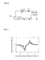
FIG. 10 is a circuit diagram schematically showing an operation verification/resistance measurement circuit for aswitching element 100 according to one embodiment of the invention. -
FIG. 11 is a graph showing current/voltage characteristic measurement results for aswitching element 100 according to one embodiment of the invention. -
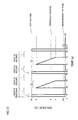
FIG. 12 is a graph schematically showing a repeated switching operation voltage sequence for aswitching element 100 according to one embodiment of the invention. -
FIG. 13 is a graph showing the resistance of aswitching element 100 according to one embodiment of the invention during repeated switching operations. -
FIG. 14 is a graph showing the resistance of aswitching element 100 according to one embodiment of the invention in the OFF state with respect to the voltage of an OFF pulse. - Examples of preferred embodiments of the invention are described below with reference to the drawings.
-
FIG. 1 is a cross-sectional view schematically showing the main portion of aswitching element 100 according to one embodiment of the invention.FIG. 2 is an enlarged cross-sectional view schematically showing the main portion of theswitching element 100.FIG. 3 is a plan view schematically showing the main portion of theswitching element 100 according to this embodiment.FIG. 4 is a schematic view showing an example in which a sealing member is provided over theswitching element 100 to form aswitching device 1000. - The
switching element 100 according to this embodiment includes aninsulating substrate 10, afirst electrode 20 provided on theinsulating substrate 10, asecond electrode 30 provided on theinsulating substrate 10, and aninterelectrode gap 40 provided between thefirst electrode 20 and thesecond electrode 30, wherein a distance G between thefirst electrode 20 and thesecond electrode 30 is 0 mn<G≤50 nm. - The
insulating substrate 10 has a function of a support which allows the twoelectrodes switching element 100 to be provided at an interval. The structure and the material for theinsulating substrate 10 are not particularly limited insofar as theinsulating substrate 10 exhibits insulating properties. For example, the surface of theinsulating substrate 10 may be flat, or may have elevations or depressions. For example, a substrate produced by forming an oxide film or the like on the surface of a semiconductor substrate (e.g., Si substrate) may be used as theinsulating substrate 10. Theinsulating substrate 10 may be an insulating substrate on which an oxide film or the like is not formed. As the material for theinsulating substrate 10, glass, an oxide such as silicon oxide (SiO2), or a nitride such as silicon nitride (Si3N4) is suitably used. In particular, silicon oxide (SiO2) is preferable as the material for the insulatingsubstrate 10 from the viewpoint of adhesion to theelectrodes - The
first electrode 20 is provided on the insulatingsubstrate 10. Thefirst electrode 20 is one electrode of theswitching element 100, and makes a pair with thesecond electrode 30 described later to enable a switching operation. The shape of thefirst electrode 20 is arbitrary. It is desirable that at least a lateral dimension (width) W1 (seeFIG. 3 ) of a portion of thefirst electrode 20 which faces thesecond electrode 30 be in the range of 5 nm≤W1. A thickness T1 of the first electrode 20 (seeFIGS. 1 and 2 ) is arbitrary. It is desirable that the thickness T1 be in the range of 5 nm≤T1 in a state in which thesecond electrode 30 is formed.FIGS. 1 and 2 illustrate an example in which thefirst electrode 20 includes a first electrodelower portion 22 and a first electrodeupper portion 24 for convenience of description relating to production steps described later. It is preferable that the material for thefirst electrode 20 be at least one material selected from gold, silver, platinum, palladium, nickel, aluminum, cobalt, chromium, rhodium, copper, tungsten, tantalum, carbon, and alloys thereof. Different metals may be used in layers in order to increase adhesion to the insulatingsubstrate 10. For example, thefirst electrode 20 may have a stacked structure of chromium and gold. - The
second electrode 30 is provided on the insulatingsubstrate 10. Thesecond electrode 30 is the other electrode of theswitching element 100, and makes a pair with thefirst electrode 20 to enable a switching operation. The shape of thesecond electrode 30 is arbitrary. It is desirable that at least a lateral dimension (width) W2 (seeFIG. 3 ) of a portion of thesecond electrode 30 which faces thefirst electrode 20 be in the range of 5 nm≤W2≤W1. A thickness T2 of thesecond electrode 30 is arbitrary. It is desirable that the thickness T2 be in the range of 5 nm≤T2≤T1 from the viewpoint of the strength of the electrode and the peel strength from the support. It is preferable that the material for thesecond electrode 30 be selected from gold, silver, platinum, palladium, nickel, aluminum, cobalt, chromium, rhodium, copper, tungsten, tantalum, carbon, and alloys thereof. Different metals may be used in layers in order to increase adhesion to the insulatingsubstrate 10. For example, thesecond electrode 30 may have a stacked structure of chromium and gold. - The
interelectrode gap 40 is provided so that the distance G between thefirst electrode 20 and thesecond electrode 30 is 0 nm < G ≤ 50 nm (e.g., 0.1 mn ≤ G ≤ 20 nm) (seeFIG. 2 ). The distance G is more preferably 0.1 mn ≤ G ≤ 10 nm. Theinterelectrode gap 40 has a function of causing a switching phenomenon of theswitching element 100. The closest interelectrode portion may be formed at one or more locations in a region in which thefirst electrode 20 faces thesecond electrode 30. If the distance G exceeds 50 nm, an electric field for theswitching element 100 to operate becomes insufficient due to the movement of metal elements. If the distance G is 0 nm, thefirst electrode 20 and thesecond electrode 30 are short-circuited. The lower limit may be referred to as the minimum distance at which a tunneling current may occur, although determination based on microscopy measurement is difficult. Specifically, the lower limit is a theoretical value of the distance at which current-voltage characteristics do not follow Ohm's law when the element operates and a quantum-mechanical tunneling effect is observed. - A sealing
member 50 may be provided to include at least theinterelectrode gap 40. It is desirable that the sealingmember 50 enclose the entire element including the insulatingsubstrate 10. The sealingmember 50 has a function of preventing theinterelectrode gap 40 from contacting the atmosphere. The shape of and the material for the sealingmember 50 are arbitrary insofar as the sealingmember 50 has the above function. The sealingmember 50 allows the switchingelement 100 to operate more stably. As the material for the sealingmember 50, a known semiconductor sealing material may be used. A gas barrier layer or the like formed of a known substance may be provided, if necessary. When the entire nanogap electrodes are placed in an appropriate vacuum chamber and used as a switching element, the sealingmember 50 may be omitted. - The inside of the sealing
member 50 may be under reduced pressure, or may be filled with various substances. The pressure inside the sealingmember 50 may be set at 2×10⁵ Pa or less. More preferably, a pressure P inside the sealingmember 50 or inside a vacuum chamber in which the nanogap electrodes are placed is set at 10-9 Pa < P < 2×10⁵ Pa. The inside of the sealingmember 50 may be filled with an inert gas such as dry air, nitrogen, or rare gas or an electrically inert organic solvent such as toluene. - A method of producing the switching
element 100 may include the following steps. - Specifically, the method of producing the switching
element 100 includes (1) a step of providing the insulatingsubstrate 10, (2) a first resist pattern formation step, (3) a first deposition step, (4) a first lift-off step, (5) a second resist pattern formation step, (6) a second deposition step, (7) a second lift-off step, (8) an electric field separation step, and (9) a sealing step. The following description is given taking an example in which thefirst electrode 20 includes the first electrodelower portion 22 and the first electrodeupper portion 24 for convenience of description relating to the production steps. The reference numerals are provided in the same manner as inFIG. 1 . - These steps are disclosed in
JP-A-2005-79335 JP-A-2004-259748 JP-A-2005-175164 element 100 is produced in accordance with the method disclosed inJP-A-2005-79335 FIGS. 1 to 6 .FIG. 5 is a schematic view illustrative of the first deposition step.FIG. 6 is a schematic view showing a circuit formed in the electric field separation step. - (1) Step of providing insulating
substrate 10
As the insulatingsubstrate 10, a commercially-available glass substrate, an Si substrate provided with an oxide film, or another substrate having an insulating surface may be used. When using a conductive substrate such as an Si substrate, a desired insulating film may be formed on the surface of the conductive substrate using a known method such as a heat treatment, an oxidation treatment, deposition, or sputtering, and the resulting substrate may be used as the insulatingsubstrate 10. - (2) First resist pattern formation step
A resistpattern 60 for forming the first electrodelower portion 22 is formed on the insulatingsubstrate 10 using a known method such as photolithography. The thickness of the resistpattern 60 is arbitrary insofar as the function of the resistpattern 60 is not impaired. For example, the thickness of the resistpattern 60 may be set at 1 micrometer. - (3) First deposition step
The first electrodelower portion 22 is formed by the first deposition step. This step may be carried out using a known deposition device. The insulatingsubstrate 10 is disposed so that the deposition target surface is inclined when viewed from a deposition source. As shown inFIG. 5 , when the angle formed by the deposition target surface and a travel direction of particles evaporated from the deposition source is referred to as θ1, the insulatingsubstrate 10 is disposed so that 0°< θ1 < 90° is satisfied (this deposition method is hereinafter referred to as "oblique deposition"). As a result, the first electrodelower portion 22 is formed in such a shape that the end face inclines, as shown inFIG. 5 . The angle formed by the inclination of the end face of the first electrodelower portion 22 and the surface of thesubstrate 10 is referred to as θ1'. The angle θ1' may be changed by adjusting the shape of the resistpattern 60, the metal deposition properties of the surface of thesubstrate 10, the angle θ1, and the like. The elements can be formed with high reproducibility when the conditions are identical. Therefore, the angle θ1' can be determined by measuring the deposition results under identical conditions.
It is preferable to increase the distance between the deposition source and the deposition target surface during deposition since the parallelism of the deposition line increases. The distance between the deposition source and the deposition target surface varies depending on the deposition device used. Deposition necessary for this embodiment can be performed when the distance between the deposition source and the deposition target surface is about 500 mm or more. In the first deposition step, a material selected from gold, silver, platinum, palladium, nickel, aluminum, cobalt, chromium, rhodium, copper, tungsten, tantalum, carbon, and alloys thereof is deposited one or more times. A plurality of deposition operations may be performed to form a two-layer structure such as depositing chromium and then depositing gold. The thickness of the first electrodelower portion 22 obtained by the first deposition step is arbitrary insofar as electric conductivity can be achieved. for example, when selecting gold as the material for the first electrodelower portion 22, the thickness of the first electrodelower portion 22 may be set at 5 nm or more. - (4) First lift-off step
The first lift-off step is carried out using a known method. In this step, a stripper suitable for the material for the resistpattern 60 is used. This step causes the first electrodelower portion 22 to be formed while removing asacrifice electrode 22a formed on the resist pattern 60 (seeFIG. 5 ). - (5) Second resist pattern formation step
A second resist pattern is formed using a known method such as photolithography. A resist pattern (not shown) for forming thesecond electrode 30 and the first electrodeupper portion 24 is formed by this step. An opening in the resist pattern is formed to cross the end (portion which serves as one of the nanogap electrodes) of the first electrodelower portion 22 obtained by the above step. The thickness of the resist pattern is arbitrary. - (6) Second deposition step
Thesecond electrode 30 is formed by the second deposition step. The first electrodeupper portion 24 is formed when forming the second electrode 30 (seeFIG. 2 ). This step may be carried out using a known deposition device. This step is carried out using oblique deposition. As shown inFIG. 2 , when the angle formed by the deposition target surface and a travel direction of particles evaporated from the deposition source is referred to as θ2, the insulatingsubstrate 10 is disposed so that 0°< θ2 < θ1'< 90° is satisfied when θ1'< 90°, and 0°<θ 2< 90° is satisfied when 90°≤ θ1'. The end (i.e., portion which faces the first electrode 20) of thesecond electrode 30 is formed by this step. The first electrodeupper portion 24 is also formed by this step. It is preferable to increase the distance between the deposition source and the deposition target surface during deposition since the parallelism of the travel path of the deposition particles increases in the same manner as in the first deposition step. The distance between the deposition source and the deposition target surface varies depending on the device used. Deposition can be performed without causing a problem when the distance between the deposition source and the deposition target surface is about 500 mm or more. In the second deposition step, a material selected from gold, silver, platinum, palladium, nickel, aluminum, cobalt, chromium, rhodium, copper, tungsten, tantalum, carbon, and alloys thereof is deposited one or more times.
Theinterelectrode gap 40 is formed utilizing the shadow of the first electrodelower portion 22 formed by deposition particles during oblique deposition in the second deposition step. Therefore, aninterelectrode gap 40 having a desired electrode-to-electrode distance G can be obtained by adjusting at least one of the thickness of the first electrodelower portion 22 and the oblique deposition angle θ2 in the second deposition step. Therefore, it is desirable that the thickness of thesecond electrode 30 obtained by the second deposition step be smaller than the thickness of thefirst electrode 20. - (7) Second lift-off step
The second lift-off step is carried out using a known method. In this step, a stripper suitable for the material of the resist pattern is used. This causes thefirst electrode 20 and thesecond electrode 30 to be formed, whereby nanogap electrodes are obtained. - (8) Electric field separation step
The nanogap electrodes thus obtained may be short-circuited. Therefore, this step may be carried out, if necessary. The electric field separation step may be carried out using a method described in Appl. Phys. Lett., 75 (1999) 301.FIG. 6 is a schematic view showing a circuit when performing the electric field separation step. A variable resistor Rv, a fixed resistor Rc, and a power supply are connected in series with the short-circuited electrodes. The fixed resistor Rc is provided to prevent a situation in which a current in an amount equal to or larger than the desired amount flows to break the electrodes. The amount of current necessary for separating the electrodes is several to several tens of milliamperes (mA). The resistance of the variable resistor Rv is slowly reduced from the initial value (high resistance) and the adjustment is stopped when the flow of current has stopped, whereby nanogap electrodes (i.e., switching element 100) having a desired electrode-to-electrode distance G can be obtained. - (9) Sealing step
This step is carried out using known hermetic seal technology. This step may be carried out with ceramic sealing, glass sealing, plastic sealing, or metal cap sealing, and may be also be carried out in a desired atmosphere. - The switching
element 100 according to this embodiment has a very simple structure and can perform stable and repeated switching operations. Specifically, the switchingelement 100 according to this embodiment has a very simple structure in which theswitching element 100 includes only the nanogap electrodes and does not require other organic molecules or inorganic particles. Since theswitching element 100 according to this embodiment does not include a substance which deteriorates, the switchingelement 100 can stably perform repeated switching operations. Moreover, the switchingelement 100 according to this embodiment is nonvolatile. - An example of the operation of the
switching element 100 according to this embodiment is described below.FIG. 7 schematically shows an example of a current-voltage curve of theswitching element 100. InFIG. 7 , the horizontal axis indicates a voltage applied between the nanogap electrodes of theswitching element 100, and the vertical axis indicates current.FIG. 7 contains symbols A to H and 0 for convenience.FIG. 8 schematically shows the sequence of the voltage applied between the nanogap electrodes of theswitching element 100. InFIG. 8 , the horizontal axis indicates the elapsed time, and the vertical axis indicates the applied voltage. - As shown in
FIG. 7 , since the current-voltage curve of theswitching element 100 is symmetrical with respect to thepoint 0, the voltage applied to theswitching element 100 and the current do not depend on the polarity of theswitching element 100. The following description focuses on the right portion (i.e., voltage is positive) ofFIG. 7 . Description of the portion in which the voltage is negative is omitted. The switching operation relating to the portion in which the voltage is negative corresponds the case where the polarity is reversed. In the region shown inFIG. 7 which passes through the point B between the point A (voltage when the resistance is minimum) and the C point, the switchingelement 100 shows a negative resistance effect whereby the resistance increases as the applied voltage increases. In this region, the state of theswitching element 100 changes depending on the applied voltage. This voltage region is hereinafter referred to as a transition region. When the voltage in the transition region is instantaneously changed to a value around the point 0 (value between the point A and the E point in practice) (the operation of instantaneously changing the voltage to a value around thepoint 0 is hereinafter referred to as "voltage-cut operation"), the resistance corresponding to the voltage applied to the element immediately before cutting the voltage can be obtained. The resistance of the element decreases as the voltage in the transition state which determines the resistance is set closer to the point A, and decreases as the voltage is set to be higher than the point A (the voltage dependence of the resistance in the transition region is described later in "5. Examples" with reference toFIG. 14 ). The point B in the transition region indicates a point at which an intermediate state between a state in which the resistance is low (hereinafter referred to as "ON state") and a state in which the resistance is high (hereinafter referred to as "OFF state") after the voltage-cut operation. The voltage at the low-voltage-side edge (around the point A) of the transition region is referred to as a threshold voltage. A value around the point A is defined as the threshold value because the threshold value (i.e., voltage at which the minimum element resistance can be obtained in the transition region) does not necessarily coincide with the point A shown inFIG. 7 and may differ to some extent from the point A depending on the operating voltage, the measurement environment, and the like. - An example of a method of operating the switching
element 100 is described below. A state J in which the voltage is instantaneously cut is obtained by applying a rectangular pulse indicated by I inFIG. 8 . The applied voltage of the rectangular pulse I corresponds to the point C which is higher in voltage than the point B in the transition region inFIG. 7 . It is desirable that the rectangular pulse width be 1 ns or more. A state in which the voltage is cut to about 0 is the region J shown inFIG. 8 . The region J corresponds to the region around thepoint 0 inFIG. 7 . In this case, when a low voltage indicated as a measurement voltage inFIG. 7 is applied, a current does not follow the curve D inFIG. 7 and has an extremely small current value. Specifically, the OFF state is obtained. A state L in which the voltage is cut is then obtained by applying a rectangular pulse indicated by K inFIG. 8 . The applied voltage of the rectangular pulse K corresponds to a voltage around the threshold voltage lower than the point B in the transition region inFIG. 7 . It is desirable that the pulse width of the rectangular pulse K be 100 ns or more. When a low voltage is applied in a region L and the current value is measured, a current follows the curve D inFIG. 7 (i.e., current flows through the element). Specifically, the ON state is obtained. The switching operation is possible since the element can be arbitrarily turned ON/OFF depending on the voltage applied before the voltage-cut operation. - When obtaining the ON state, the period in which the applied voltage is set at about the threshold voltage is important. Specifically, it is desirable that the period in which the applied voltage is set at about the threshold voltage be 100 ns or more. When this condition is satisfied, a triangular wave indicated by N in
FIG. 8 may be used instead of the rectangular wave K in order to obtain the ON state. The triangular wave N must have a vertex at a voltage higher than the threshold value so that the triangular wave N crosses a voltage around the threshold voltage. The period in which the applied voltage is set to be higher than the threshold voltage is adjusted by adjusting a slope Q of the triangular wave N inFIG. 8 . The ON state is obtained by adjusting the slope Q so that the period in which the applied voltage is set at about the threshold voltage is 100 ns or more. On the other hand, when the period of the triangular wave in which the applied voltage is set at about the threshold voltage is very short (in this case, it is desirable that the period in which the applied voltage is set at about the threshold voltage be 100 ns or less) (i.e., when a triangular wave M inFIG. 8 is applied), the element is turned OFF. Specifically, it is possible to use the triangular wave M instead of the rectangular wave I in order to obtain the OFF state. The value of the vertex of the triangular wave M is set at the point C inFIG. 7 in the same manner as the rectangular wave I. The period in which the applied voltage is set at about the threshold voltage is adjusted by adjusting the slope of the triangular wave M in a region P inFIG. 8 . - The switching
element 100 may be driven using various sequences other than the above-described rectangular wave and triangular wave. - As the insulating
substrate 10, a silicon substrate coated with a silicon oxide layer with a thickness of 300 nm was used. The thickness of the first resist pattern was set at 1 micrometer. The first resist pattern was formed so that the width W1 of the first electrodelower portion 22 in the horizontal direction was 100 micrometers. The first electrodelower portion 22 was formed by depositing chromium on the insulatingsubstrate 10 to a thickness of 2 nm and then depositing gold so that the total thickness was 25 nm. The angle θ1 during oblique deposition in the first deposition step was set at 75°. The thickness of the second resist pattern was set at 1 micrometer. The second resist pattern was formed so that the width W2 of thesecond electrode 30 in the horizontal direction was 2 micrometers. Thesecond electrode 30 was formed by depositing chromium on the insulatingsubstrate 10 to a thickness of 2 nm and then depositing gold so that the total thickness was 15 nm. Therefore, the total thickness of thefirst electrode 20 was about 40 nm. The angle θ2 during oblique deposition in the second deposition step was set at 60°. The second lift-off step was then carried out. Since thefirst electrode 20 and thesecond electrode 30 of theswitching element 100 in this state were partially short-circuited, the short-circuited portion was removed by performing the electric field separation step. The electric field separation conditions were as follows. The applied voltage was 1 V, and the resistance of the resistor Rc was 100 ohms. The resistance of the variable resistor Rv was gradually decreased from 100 kilohms to 0 ohm so that the amount of current was gradually increased. The amount of current when electric field separation occurred was about 4 mA. The switchingelement 100 was thus obtained. The resultingswitching element 100 was placed in a vacuum chamber. The pressure inside the vacuum chamber was about 10-5 Pa. -
FIG. 9 shows an observation result for theswitching element 100 according to this example using a scanning electron microscope. The switchingelement 100 was photographed at a accelerating voltage of 15 kV using a scanning electron microscope S-4300 (manufactured by Hitachi, Ltd.). The scanning speed was increased using a heating stage (resolution: about 5 nm).FIG. 9 shows part of the first electrode 20 (upper side), part of the second electrode 30 (lower side), and part of the interelectrode gap 40 (horizontally extending dark portion at the center of the photograph). As shown inFIG. 9 , the first electrode is positioned close to the second electrode at a plurality of points in theinterelectrode gap 40. A downward bold arrow indicates a portion in which the electrodes are closely positioned. Two lines which indicate the width of the gap are drawn on the left of each arrow. The width of each gap was measured. The distance G between thefirst electrode 20 and thesecond electrode 30 in the observed area was about 8 nm. A portion in which the two electrodes of theswitching element 100 are closely positioned may exist in an area other than the observed area. When the electrodes are positioned at a shorter distance, the distance cannot be measured due to the resolution of the microscope. The shortest distance between the electrodes was estimated from the resistance. The resistance between the electrodes was about 60 kilohms when the element was turned ON. Therefore, the shortest distance between the electrodes was at least 0.1 nm or more based on calculations from the tunneling effect. -
FIG. 10 is a schematic view showing a circuit used to evaluate the element characteristics. The evaluation circuit was formed by connecting theswitching element 100 to a micro-prober device in a vacuum chamber.FIG. 11 is a graph showing the measurement results for the I-V characteristics of theswitching element 100 according to this embodiment using the circuit shown inFIG. 10 . The horizontal axis of the graph shown inFIG. 11 indicates the net voltage applied to theswitching element 100 obtained by subtracting voltage across the fixed resistor Rm from the circuit voltage. InFIG. 10 , the vertical axis indicates a current which flows when applying each voltage measured using an ammeter. The I-V characteristics shown inFIG. 11 were measured as follows. The applied voltage was set at 0 V when starting the measurement. The applied voltage was swept to +15 V at a sweep rate of +0.2 V/s, swept to -15 V at a sweep rate of -0.2 V/s, and swept to +15 V at a sweep rate of +0.2 V/s. This cycle was repeated.FIG 11 corresponds toFIG 7 . - In the I-V curve of the
switching element 100 according to this embodiment shown inFIG. 11 , the absolute value of the current is maximized when the applied voltage is +4 V and -4 V. The absolute value of the current rapidly decreases when the voltage is higher than +4 V. The absolute value of the current rapidly decreases when the voltage is lower than -4 V. The switching operation was performed as described in "4. Switching operation" utilizing this phenomenon. Specifically, a voltage (absolute value) of about 4 V was set to be the threshold voltage (corresponding to a point around the points A, B, E, and F inFIG. 7 ). -
FIG. 12 is a schematic view of the voltage sequence according to this example. In this example, the voltage of the pulse which causes the element to be turned OFF was set at +10 V. The voltage of the triangular wave which causes the element to be turned ON was swept from +9 V to +3 V and was cut at +3 V. As shown inFIG. 12 , the rectangular pulse I at +10 V was applied for 100 ms, and the resistance was measured in the region J for about 24 seconds at a measurement voltage of +0.2 V. As indicated by the region K inFIG. 12 , the voltage was swept from +9 V to +3 V over one minute and then cut. The resistance was measured in the region L for about 24 seconds at a measurement voltage of +0.2 V. The resistance was measured by performing theabove cycle 1000 times. -
FIG. 13 shows part of the resistance measurement results according to this example. InFIG. 13 , the horizontal axis indicates the elapsed time, and the vertical axis indicates the resistance when applying a voltage of +0.2 V. As shownFIG. 13 , the resistance of theswitching element 100 according to this embodiment in the ON state and the OFF state changed to only a small extent from the initial value during the repeated ON/OFF operations. The resistance in the ON state and the OFF state changed to only a small extent from the initial value even after the 1000-cycle measurements. Specifically, the resistance between thefirst electrode 20 and thesecond electrode 30 of theswitching element 100 was 10 to 200 kilohms in the ON state and was 100 megaohms to 10 gigaohms in the OFF state. - This indicates that the switching
element 100 can be arbitrarily turned ON/OFF depending on the voltage input from the outside. Since the ON/OFF state of the element can be maintained after applying the voltage pulse, even if the voltage is not applied, the switchingelement 100 is a nonvolatile switching element. -
FIG. 14 is a graph in which the horizontal axis indicates the voltage of the pulse which causes the element to be turned OFF and the vertical axis indicates the resistance across the switchingelement 100 immediately after applying the pulse. With reference toFIG. 12 , the horizontal axis ofFIG. 14 indicates the voltage of the 100-ms rectangular pulse I and the vertical axis indicates the resistance measured in the region J during repeated measurements. As shown inFIG. 14 , the resistance exceeds 1 megaohm when the voltage of the pulse exceeds about +5 V so that the OFF state is achieved. When the voltage of the pulse exceeds about +10 V, the resistance exceeds 10 gigaohms. When the voltage of the pulse exceeds about +13 V, the resistance exceeds 1 teraohm. Specifically, the switchingelement 100 is a switching element of which the resistance in the OFF state can be arbitrarily set depending on the voltage of the pulse which causes the switching element to be turned OFF. Since the ON state can obtained at about +4 V, the switchingelement 100 can be arbitrarily set in at least four resistance states. Specifically, the resistance can be set at 10 kilohms to 1 megaohm when the switching element is turned ON, and can be set at 1 megaohm to 100 teraohms when the switching element is turned OFF. The resistance of the switching element using the nanogap electrodes can be set at several to 100 kilohms in the ON state, and can be set at several hundred kilohms to several gigaohms in the OFF state, for example. It is possible to utilize the switching element as an element which can generate a relatively low resistance and a high resistance by arbitrarily selecting two states from these resistance states. - As described above, the switching
element 100 according to this embodiment is a very simple switching element which does not use organic molecules, nanoparticles, and the like. Moreover, the switchingelement 100 can repeat switching operations in an extremely stable manner. Specifically, the switchingelement 100 according to this embodiment is a nonvolatile switching element which has a very simple structure and can perform stable and repeated switching operations.
Claims (8)
- A switching element comprising:an insulating substrate;a first electrode provided on the insulating substrate;a second electrode provided on the insulating substrate; andan interelectrode gap provided between the first electrode and the second electrode, a distance G between the first electrode and the second electrode being 0 nm < G ≤ 50 nm.
- The switching element as defined in claim 1,
wherein the distance G between the first electrode and the second electrode is 0.1 nm≤G≤20nm. - The switching element as defined in claim 1, further comprising:a sealing member which includes at least the interelectrode gap.
- The switching element as defined in claim 3,
wherein a pressure inside the sealing member is 2×10⁵ Pa or less. - The switching element as defined in any one of claims 1 to 4,
wherein a material for the first electrode is at least one material selected from gold, silver, platinum, palladium, nickel, aluminum, cobalt, chromium, rhodium, copper, tungsten, tantalum, carbon, and alloys thereof. - The switching element as defined in any one of claims 1 to 4,
wherein a material for the second electrode is at least one material selected from gold, silver, platinum, palladium, nickel, aluminum, cobalt, chromium, rhodium, copper, tungsten, tantalum, carbon, and alloys thereof. - The switching element as defined in any one of claims 1 to 4,
wherein at least one of the first electrode and the second electrode has a multilayer structure. - The switching element as defined in any one of claims 1 to 4,
wherein a resistance between the first electrode and the second electrode is 1 kilohm to 1 megaohm when the switching element is turned ON, and is 1 megaohm to 100 teraohms when the switching element is turned OFF.
Applications Claiming Priority (3)
| Application Number | Priority Date | Filing Date | Title |
|---|---|---|---|
| JP2005280633 | 2005-09-27 | ||
| JP2006189380A JP4919146B2 (en) | 2005-09-27 | 2006-07-10 | Switching element |
| PCT/JP2006/318993 WO2007037210A1 (en) | 2005-09-27 | 2006-09-25 | Switching element |
Publications (3)
| Publication Number | Publication Date |
|---|---|
| EP1939941A1 true EP1939941A1 (en) | 2008-07-02 |
| EP1939941A4 EP1939941A4 (en) | 2010-09-08 |
| EP1939941B1 EP1939941B1 (en) | 2012-06-06 |
Family
ID=37899636
Family Applications (1)
| Application Number | Title | Priority Date | Filing Date |
|---|---|---|---|
| EP06798318A Not-in-force EP1939941B1 (en) | 2005-09-27 | 2006-09-25 | Method of operating a switching element |
Country Status (6)
| Country | Link |
|---|---|
| US (1) | US8093518B2 (en) |
| EP (1) | EP1939941B1 (en) |
| JP (1) | JP4919146B2 (en) |
| KR (1) | KR100990504B1 (en) |
| CN (1) | CN101273461B (en) |
| WO (1) | WO2007037210A1 (en) |
Cited By (3)
| Publication number | Priority date | Publication date | Assignee | Title |
|---|---|---|---|---|
| EP2006928A3 (en) * | 2007-06-22 | 2012-05-30 | Funai Electric Co., Ltd. | Switching element |
| EP2028693A3 (en) * | 2007-08-22 | 2012-06-06 | Funai Electric Advanced Applied Technology Research Institute Inc. | Switching element, method of manufacturing the switching element, and memory element array |
| EP2006912A3 (en) * | 2007-06-22 | 2012-06-06 | Funai Electric Co., Ltd. | Memory element array comprising a switching element with a nanogap and a tunnel element |
Families Citing this family (19)
| Publication number | Priority date | Publication date | Assignee | Title |
|---|---|---|---|---|
| JP4919146B2 (en) | 2005-09-27 | 2012-04-18 | 独立行政法人産業技術総合研究所 | Switching element |
| JP2008311449A (en) * | 2007-06-15 | 2008-12-25 | National Institute Of Advanced Industrial & Technology | Two-terminal resistance switch element and semiconductor device using silicon |
| JP5190924B2 (en) * | 2007-08-09 | 2013-04-24 | 独立行政法人産業技術総合研究所 | Two-terminal resistance switch element and semiconductor device |
| JP5312782B2 (en) * | 2007-12-20 | 2013-10-09 | 株式会社船井電機新応用技術研究所 | Nanogap switching element driving method and storage device including nanogap switching element |
| JP4544340B2 (en) | 2008-01-24 | 2010-09-15 | ソニー株式会社 | ELECTRONIC DEVICE, ITS MANUFACTURING METHOD, AND STORAGE DEVICE |
| JP5120883B2 (en) * | 2008-02-26 | 2013-01-16 | 株式会社船井電機新応用技術研究所 | Nanogap device driving method and storage device including nanogap device |
| WO2009150751A1 (en) * | 2008-06-13 | 2009-12-17 | 株式会社船井電機新応用技術研究所 | Switching element |
| JP5415049B2 (en) * | 2008-09-26 | 2014-02-12 | 株式会社船井電機新応用技術研究所 | Memory device, memory device manufacturing method, and memory array |
| JP5419408B2 (en) * | 2008-09-26 | 2014-02-19 | 株式会社船井電機新応用技術研究所 | Memory device, memory device manufacturing method, memory array configuration element, and memory array |
| JP5526341B2 (en) * | 2010-02-25 | 2014-06-18 | 独立行政法人産業技術総合研究所 | Switching element |
| JP5499364B2 (en) | 2010-08-26 | 2014-05-21 | 独立行政法人産業技術総合研究所 | Memory element driving method and memory device including memory element |
| JP5527729B2 (en) | 2010-08-26 | 2014-06-25 | 独立行政法人産業技術総合研究所 | Memory element driving method and memory device including memory element |
| JP5900872B2 (en) * | 2011-03-08 | 2016-04-06 | 国立研究開発法人産業技術総合研究所 | Electronic device and method for manufacturing electronic device |
| KR102123955B1 (en) * | 2013-03-09 | 2020-06-17 | 고쿠리츠켄큐카이하츠호진 카가쿠기쥬츠신코키코 | Electronic element |
| JP2015060890A (en) | 2013-09-17 | 2015-03-30 | 株式会社東芝 | Storage device |
| US10396175B2 (en) | 2014-11-25 | 2019-08-27 | University Of Kentucky Research Foundation | Nanogaps on atomically thin materials as non-volatile read/writable memory devices |
| JP6886304B2 (en) | 2017-01-31 | 2021-06-16 | ヌヴォトンテクノロジージャパン株式会社 | Gas sensor |
| HRP20240756T1 (en) * | 2018-05-18 | 2024-09-13 | Daiichi Sankyo Co., Ltd. | Anti-muc1- exatecan antibody-drug conjugate |
| CN109911838B (en) * | 2019-02-25 | 2021-01-19 | 华中科技大学 | Complementary resistance switch device realized based on controllable nano-cracks and control method thereof |
Family Cites Families (65)
| Publication number | Priority date | Publication date | Assignee | Title |
|---|---|---|---|---|
| US3971056A (en) * | 1975-02-18 | 1976-07-20 | Cutler-Hammer, Inc. | Semiconductor temperature switches |
| US4112458A (en) * | 1976-01-26 | 1978-09-05 | Cutler-Hammer, Inc. | Silicon thyristor sensitive to low temperature with thermal switching characteristics at temperatures less than 50° C |
| US4814943A (en) * | 1986-06-04 | 1989-03-21 | Oki Electric Industry Co., Ltd. | Printed circuit devices using thermoplastic resin cover plate |
| US5208693A (en) * | 1991-03-29 | 1993-05-04 | Raynet Corporation | Transmission protocol for clamping receiver |
| US5412498A (en) * | 1991-03-29 | 1995-05-02 | Raynet Corporation | Multi-RC time constant receiver |
| US5339211A (en) * | 1991-05-02 | 1994-08-16 | Dow Corning Corporation | Variable capacitor |
| US5285619A (en) * | 1992-10-06 | 1994-02-15 | Williams International Corporation | Self tooling, molded electronics packaging |
| US5648296A (en) * | 1994-07-27 | 1997-07-15 | General Electric Company | Post-fabrication repair method for thin film imager devices |
| JP3062029B2 (en) * | 1995-01-31 | 2000-07-10 | 日本電気株式会社 | Temperature detection method using forward voltage of diode |
| US6057038A (en) * | 1996-08-02 | 2000-05-02 | Sharp Kabushiki Kaisha | Substrate for use in display element, method of manufacturing the same, and apparatus for manufacturing the same |
| JP3030333B2 (en) | 1997-03-14 | 2000-04-10 | 工業技術院長 | Switching device and memory device using current and electric field induced phase transition |
| US6163055A (en) * | 1997-03-24 | 2000-12-19 | Semiconductor Energy Laboratory Co., Ltd | Semiconductor device and manufacturing method thereof |
| ATE235093T1 (en) | 1997-12-04 | 2003-04-15 | Axon Technologies Corp | PROGRAMMABLE METALLIZATION STRUCTURE WITH NEAR-SURFACE SOLIDIFICATION AND PRODUCTION PROCESS THEREOF |
| US6548843B2 (en) * | 1998-11-12 | 2003-04-15 | International Business Machines Corporation | Ferroelectric storage read-write memory |
| US6391675B1 (en) * | 1998-11-25 | 2002-05-21 | Raytheon Company | Method and apparatus for switching high frequency signals |
| US6635914B2 (en) * | 2000-09-08 | 2003-10-21 | Axon Technologies Corp. | Microelectronic programmable device and methods of forming and programming the same |
| JP3595744B2 (en) * | 1999-02-26 | 2004-12-02 | キヤノン株式会社 | Electron emitting element, electron source and image forming apparatus |
| US6509619B1 (en) * | 1999-09-10 | 2003-01-21 | Starmega Corporation | Strongly textured atomic ridge and dot Mosfets, sensors and filters |
| WO2001039292A2 (en) * | 1999-11-29 | 2001-05-31 | Trustees Of The University Of Pennsylvania | Fabrication of nanometer size gaps on an electrode |
| US6483719B1 (en) * | 2000-03-21 | 2002-11-19 | Spraylat Corporation | Conforming shielded form for electronic component assemblies |
| US6791648B2 (en) * | 2001-03-15 | 2004-09-14 | Seiko Epson Corporation | Liquid crystal device, projection display device and, manufacturing method for substrate for liquid crystal device |
| US6900383B2 (en) * | 2001-03-19 | 2005-05-31 | Hewlett-Packard Development Company, L.P. | Board-level EMI shield that adheres to and conforms with printed circuit board component and board surfaces |
| US6996147B2 (en) * | 2001-03-30 | 2006-02-07 | The Regents Of The University Of California | Methods of fabricating nanostructures and nanowires and devices fabricated therefrom |
| US6614102B1 (en) * | 2001-05-04 | 2003-09-02 | Amkor Technology, Inc. | Shielded semiconductor leadframe package |
| US6803534B1 (en) * | 2001-05-25 | 2004-10-12 | Raytheon Company | Membrane for micro-electro-mechanical switch, and methods of making and using it |
| US6919592B2 (en) * | 2001-07-25 | 2005-07-19 | Nantero, Inc. | Electromechanical memory array using nanotube ribbons and method for making same |
| US6891319B2 (en) * | 2001-08-29 | 2005-05-10 | Motorola, Inc. | Field emission display and methods of forming a field emission display |
| US6699779B2 (en) * | 2002-03-22 | 2004-03-02 | Hewlett-Packard Development Company, L.P. | Method for making nanoscale wires and gaps for switches and transistors |
| US6791441B2 (en) * | 2002-05-07 | 2004-09-14 | Raytheon Company | Micro-electro-mechanical switch, and methods of making and using it |
| JP4186727B2 (en) * | 2002-07-26 | 2008-11-26 | 松下電器産業株式会社 | switch |
| JP4224579B2 (en) * | 2003-02-24 | 2009-02-18 | 独立行政法人産業技術総合研究所 | Electrode manufacturing method of electrode cross-linking molecular device and manufacturing method of electrode cross-linking molecular device |
| WO2005008450A2 (en) * | 2003-03-28 | 2005-01-27 | The Regents Of The University Of California | Method and apparatus for nanogap device and array |
| US7113426B2 (en) * | 2003-03-28 | 2006-09-26 | Nantero, Inc. | Non-volatile RAM cell and array using nanotube switch position for information state |
| JP4314867B2 (en) | 2003-04-08 | 2009-08-19 | ソニー株式会社 | Manufacturing method of MEMS element |
| US7274064B2 (en) * | 2003-06-09 | 2007-09-25 | Nanatero, Inc. | Non-volatile electromechanical field effect devices and circuits using same and methods of forming same |
| CA2528804A1 (en) * | 2003-06-09 | 2005-01-06 | Nantero, Inc | Non-volatile electromechanical field effect devices and circuits using same and methods of forming same |
| US7115960B2 (en) * | 2003-08-13 | 2006-10-03 | Nantero, Inc. | Nanotube-based switching elements |
| JP3864229B2 (en) * | 2003-08-29 | 2006-12-27 | 独立行政法人産業技術総合研究所 | Method for producing nanogap electrode and device having nanogap electrode produced by the method |
| US7015504B2 (en) * | 2003-11-03 | 2006-03-21 | Advanced Micro Devices, Inc. | Sidewall formation for high density polymer memory element array |
| KR100565174B1 (en) * | 2003-11-20 | 2006-03-30 | 한국전자통신연구원 | Manufacturing method of nanogap electrode device |
| JP3864232B2 (en) * | 2003-12-10 | 2006-12-27 | 独立行政法人産業技術総合研究所 | Manufacturing method of nanogap electrode and device using nanogap electrode manufactured by the method |
| US7164744B2 (en) * | 2004-06-18 | 2007-01-16 | Nantero, Inc. | Nanotube-based logic driver circuits |
| JP2006128438A (en) * | 2004-10-29 | 2006-05-18 | National Institute Of Advanced Industrial & Technology | Method of forming nanogap electrode, nanogap electrode obtained thereby, and device provided with the electrode |
| JP4475098B2 (en) | 2004-11-02 | 2010-06-09 | ソニー株式会社 | Storage element and driving method thereof |
| JP4783045B2 (en) * | 2004-11-17 | 2011-09-28 | 株式会社東芝 | Switching element |
| WO2006070698A1 (en) * | 2004-12-27 | 2006-07-06 | Nec Corporation | Switching device, driving method and manufacturing method of switching device, integrated circuit device, and memory device |
| KR100679704B1 (en) | 2005-01-10 | 2007-02-06 | 한국과학기술원 | Manufacturing method of nanogap or nanofield effect transistor for molecular device and biosensor |
| US7804085B2 (en) * | 2005-01-17 | 2010-09-28 | Nec Corporation | Solid electrolyte switching element, and fabrication method of the solid electrolyte element, and integrated circuit |
| JP4701452B2 (en) | 2005-02-23 | 2011-06-15 | 独立行政法人産業技術総合研究所 | Manufacturing method of nanogap electrode |
| DE102005009057A1 (en) | 2005-02-28 | 2006-08-31 | Patent-Treuhand-Gesellschaft für elektrische Glühlampen mbH | Starter for AC fed low-pressure discharge lamp, has thermistor having high resistance, which is transformed into low resistance by self-heating, and bimetal switch to interrupt electrode heating circuit when lamp fails to ignite |
| JP4575837B2 (en) | 2005-05-19 | 2010-11-04 | シャープ株式会社 | Nonvolatile memory element and manufacturing method thereof |
| US7541227B2 (en) * | 2005-06-02 | 2009-06-02 | Hewlett-Packard Development Company, L.P. | Thin film devices and methods for forming the same |
| US20060278879A1 (en) * | 2005-06-09 | 2006-12-14 | Cabot Microelectronics Corporation | Nanochannel device and method of manufacturing same |
| JP2007049084A (en) * | 2005-08-12 | 2007-02-22 | Toshiba Corp | Switch element, memory element and magnetoresistive effect element |
| KR100682952B1 (en) * | 2005-08-31 | 2007-02-15 | 삼성전자주식회사 | Nanoelastic memory device and manufacturing method thereof |
| JP4919146B2 (en) | 2005-09-27 | 2012-04-18 | 独立行政法人産業技術総合研究所 | Switching element |
| US7449710B2 (en) * | 2005-11-21 | 2008-11-11 | Macronix International Co., Ltd. | Vacuum jacket for phase change memory element |
| US7419849B2 (en) * | 2006-02-06 | 2008-09-02 | Matsushita Electric Industrial Co., Ltd. | Method for producing single electron semiconductor element |
| WO2008064216A2 (en) * | 2006-11-20 | 2008-05-29 | Massachusetts Institute Of Technology | Micro-electro mechanical tunneling switch |
| JP4446054B2 (en) * | 2007-03-23 | 2010-04-07 | 独立行政法人産業技術総合研究所 | Nonvolatile memory element |
| JP2008311449A (en) * | 2007-06-15 | 2008-12-25 | National Institute Of Advanced Industrial & Technology | Two-terminal resistance switch element and semiconductor device using silicon |
| JP5120874B2 (en) * | 2007-06-22 | 2013-01-16 | 株式会社船井電機新応用技術研究所 | Switching element |
| KR101303579B1 (en) * | 2007-07-19 | 2013-09-09 | 삼성전자주식회사 | Electromechanical switch and method of manufacturing the same |
| JP5312782B2 (en) * | 2007-12-20 | 2013-10-09 | 株式会社船井電機新応用技術研究所 | Nanogap switching element driving method and storage device including nanogap switching element |
| WO2009150751A1 (en) * | 2008-06-13 | 2009-12-17 | 株式会社船井電機新応用技術研究所 | Switching element |
-
2006
- 2006-07-10 JP JP2006189380A patent/JP4919146B2/en not_active Expired - Fee Related
- 2006-09-25 CN CN2006800353971A patent/CN101273461B/en not_active Expired - Fee Related
- 2006-09-25 US US11/992,883 patent/US8093518B2/en not_active Expired - Fee Related
- 2006-09-25 WO PCT/JP2006/318993 patent/WO2007037210A1/en not_active Ceased
- 2006-09-25 EP EP06798318A patent/EP1939941B1/en not_active Not-in-force
- 2006-09-25 KR KR1020087010074A patent/KR100990504B1/en not_active Expired - Fee Related
Cited By (5)
| Publication number | Priority date | Publication date | Assignee | Title |
|---|---|---|---|---|
| EP2006928A3 (en) * | 2007-06-22 | 2012-05-30 | Funai Electric Co., Ltd. | Switching element |
| EP2006912A3 (en) * | 2007-06-22 | 2012-06-06 | Funai Electric Co., Ltd. | Memory element array comprising a switching element with a nanogap and a tunnel element |
| US8395185B2 (en) | 2007-06-22 | 2013-03-12 | Funai Electric Advanced Applied Technology Research Institute Inc. | Switching element |
| EP2028693A3 (en) * | 2007-08-22 | 2012-06-06 | Funai Electric Advanced Applied Technology Research Institute Inc. | Switching element, method of manufacturing the switching element, and memory element array |
| KR101449916B1 (en) * | 2007-08-22 | 2014-10-15 | 후나이 일렉트릭 어드밴스드 어플라이드 테크놀로지 리서치 인스티튜트 인코포레이티드 | Switching element, method of manufacturing switching element, and memory element array |
Also Published As
| Publication number | Publication date |
|---|---|
| CN101273461A (en) | 2008-09-24 |
| WO2007037210A1 (en) | 2007-04-05 |
| KR100990504B1 (en) | 2010-10-29 |
| JP2007123828A (en) | 2007-05-17 |
| US8093518B2 (en) | 2012-01-10 |
| CN101273461B (en) | 2010-07-14 |
| KR20080059602A (en) | 2008-06-30 |
| US20090251199A1 (en) | 2009-10-08 |
| EP1939941B1 (en) | 2012-06-06 |
| JP4919146B2 (en) | 2012-04-18 |
| EP1939941A4 (en) | 2010-09-08 |
Similar Documents
| Publication | Publication Date | Title |
|---|---|---|
| EP1939941B1 (en) | Method of operating a switching element | |
| JP4446054B2 (en) | Nonvolatile memory element | |
| CN101330127B (en) | Switching element | |
| US10090463B2 (en) | Non-volatile solid state resistive switching devices | |
| Almadhoun et al. | Bipolar resistive switching in junctions of gallium oxide and p-type silicon | |
| US8716688B2 (en) | Electronic device incorporating memristor made from metallic nanowire | |
| JP5170615B2 (en) | Switching element | |
| CN102084512B (en) | Switching element | |
| US8492231B2 (en) | Nanoscale variable resistor/electromechanical transistor | |
| US8604458B2 (en) | Two-terminal resistance switching device and semiconductor device | |
| WO2018209441A1 (en) | Method and apparatus for making a nanopore in a membrane using an electric field applied via a conductive tip | |
| JP5120872B2 (en) | Switching element | |
| Mubeen et al. | Fabrication of nanoelectrodes and nanojunction hydrogen sensor | |
| JP5526341B2 (en) | Switching element | |
| Pósa | Resistive switching in ultrasmall nanogap devices | |
| Ito et al. | Simultaneous fabrication of nanogaps using field-emission-induced electromigration | |
| Ohata et al. | Fabrication of nanogap electrode using electromigration method during metal deposition | |
| Takikawa et al. | Resistive switching effects in electromigrated Ni nanogaps | |
| Kase et al. | Field-emission-induced electromigration method for precise tuning of electrical properties of Ni-based single-electron transistors | |
| Awais | Printed Memristive Devices for Electrical Switching and Memory Applications |
Legal Events
| Date | Code | Title | Description |
|---|---|---|---|
| PUAI | Public reference made under article 153(3) epc to a published international application that has entered the european phase |
Free format text: ORIGINAL CODE: 0009012 |
|
| 17P | Request for examination filed |
Effective date: 20080401 |
|
| AK | Designated contracting states |
Kind code of ref document: A1 Designated state(s): DE FR GB PL |
|
| RBV | Designated contracting states (corrected) |
Designated state(s): DE FR GB PL |
|
| A4 | Supplementary search report drawn up and despatched |
Effective date: 20100809 |
|
| RIC1 | Information provided on ipc code assigned before grant |
Ipc: H01L 45/00 20060101AFI20100730BHEP |
|
| DAX | Request for extension of the european patent (deleted) | ||
| 17Q | First examination report despatched |
Effective date: 20110228 |
|
| REG | Reference to a national code |
Ref country code: DE Ref legal event code: R079 Ref document number: 602006029991 Country of ref document: DE Free format text: PREVIOUS MAIN CLASS: H01L0029660000 Ipc: H01L0045000000 |
|
| GRAP | Despatch of communication of intention to grant a patent |
Free format text: ORIGINAL CODE: EPIDOSNIGR1 |
|
| RIC1 | Information provided on ipc code assigned before grant |
Ipc: H01L 45/00 20060101AFI20111209BHEP |
|
| RTI1 | Title (correction) |
Free format text: METHOD OF OPERATING A SWITCHING ELEMENT |
|
| RIN1 | Information on inventor provided before grant (corrected) |
Inventor name: ONO, MASATOSHI Inventor name: TAKAHASHI, TSUYOSHI Inventor name: ABE, HIDEKAZU Inventor name: MIZUTANI, WATARU Inventor name: FURUTA, SHIGEO Inventor name: SHIMIZU, TETSUO Inventor name: NAITOH, YASUHISA Inventor name: HORIKAWA, MASAYO |
|
| GRAS | Grant fee paid |
Free format text: ORIGINAL CODE: EPIDOSNIGR3 |
|
| GRAA | (expected) grant |
Free format text: ORIGINAL CODE: 0009210 |
|
| RIN1 | Information on inventor provided before grant (corrected) |
Inventor name: NAITOH, YASUHISA Inventor name: MIZUTANI, WATARU Inventor name: SHIMIZU, TETSUO Inventor name: HORIKAWA, MASAYO Inventor name: TAKAHASHI, TSUYOSHI Inventor name: ONO, MASATOSHI Inventor name: ABE, HIDEKAZU Inventor name: FURUTA, SHIGEO |
|
| RIN1 | Information on inventor provided before grant (corrected) |
Inventor name: ONO, MASATOSHI Inventor name: MIZUTANI, WATARU Inventor name: TAKAHASHI, TSUYOSHI Inventor name: NAITOH, YASUHISA Inventor name: FURUTA, SHIGEO Inventor name: SHIMIZU, TETSUO Inventor name: HORIKAWA, MASAYO Inventor name: ABE, HIDEKAZU |
|
| AK | Designated contracting states |
Kind code of ref document: B1 Designated state(s): DE FR GB PL |
|
| REG | Reference to a national code |
Ref country code: GB Ref legal event code: FG4D |
|
| REG | Reference to a national code |
Ref country code: DE Ref legal event code: R096 Ref document number: 602006029991 Country of ref document: DE Effective date: 20120802 |
|
| PG25 | Lapsed in a contracting state [announced via postgrant information from national office to epo] |
Ref country code: PL Free format text: LAPSE BECAUSE OF FAILURE TO SUBMIT A TRANSLATION OF THE DESCRIPTION OR TO PAY THE FEE WITHIN THE PRESCRIBED TIME-LIMIT Effective date: 20120606 |
|
| REG | Reference to a national code |
Ref country code: DE Ref legal event code: R082 Ref document number: 602006029991 Country of ref document: DE Representative=s name: ROOS, PETER, DIPL.-PHYS.UNIV. DR.RER.NAT., DE Ref country code: DE Ref legal event code: R082 Ref document number: 602006029991 Country of ref document: DE Representative=s name: ROOS, PETER, DIPL.-PHYS. UNIV. DR.RER.NAT., DE |
|
| PLBE | No opposition filed within time limit |
Free format text: ORIGINAL CODE: 0009261 |
|
| STAA | Information on the status of an ep patent application or granted ep patent |
Free format text: STATUS: NO OPPOSITION FILED WITHIN TIME LIMIT |
|
| 26N | No opposition filed |
Effective date: 20130307 |
|
| REG | Reference to a national code |
Ref country code: DE Ref legal event code: R097 Ref document number: 602006029991 Country of ref document: DE Effective date: 20130307 |
|
| REG | Reference to a national code |
Ref country code: DE Ref legal event code: R082 Ref document number: 602006029991 Country of ref document: DE Representative=s name: ROOS, PETER, DIPL.-PHYS.UNIV. DR.RER.NAT., DE Ref country code: DE Ref legal event code: R081 Ref document number: 602006029991 Country of ref document: DE Owner name: FUNAI ELECTRIC CO., LTD., DAITO-SHI, JP Free format text: FORMER OWNER: FUNAI ELECTRIC ADVANCED APPLIED, NATIONAL INSTITUTE OF ADVANCED, , JP Ref country code: DE Ref legal event code: R081 Ref document number: 602006029991 Country of ref document: DE Owner name: NATIONAL INSTITUTE OF ADVANCED INDUSTRIAL SCIE, JP Free format text: FORMER OWNER: FUNAI ELECTRIC ADVANCED APPLIED, NATIONAL INSTITUTE OF ADVANCED, , JP Ref country code: DE Ref legal event code: R081 Ref document number: 602006029991 Country of ref document: DE Owner name: FUNAI ELECTRIC CO., LTD., DAITO-SHI, JP Free format text: FORMER OWNERS: FUNAI ELECTRIC ADVANCED APPLIED TECHNOLOGY RESEARCH INSTITUTE INC., DAITO-SHI, OSAKA, JP; NATIONAL INSTITUTE OF ADVANCED INDUSTRIAL SCIENCE AND TECHNOLOGY, TOKYO, JP Ref country code: DE Ref legal event code: R081 Ref document number: 602006029991 Country of ref document: DE Owner name: NATIONAL INSTITUTE OF ADVANCED INDUSTRIAL SCIE, JP Free format text: FORMER OWNERS: FUNAI ELECTRIC ADVANCED APPLIED TECHNOLOGY RESEARCH INSTITUTE INC., DAITO-SHI, OSAKA, JP; NATIONAL INSTITUTE OF ADVANCED INDUSTRIAL SCIENCE AND TECHNOLOGY, TOKYO, JP Ref country code: DE Ref legal event code: R082 Ref document number: 602006029991 Country of ref document: DE Representative=s name: ROOS, PETER, DIPL.-PHYS. UNIV. DR.RER.NAT., DE |
|
| REG | Reference to a national code |
Ref country code: GB Ref legal event code: 732E Free format text: REGISTERED BETWEEN 20150528 AND 20150603 |
|
| REG | Reference to a national code |
Ref country code: FR Ref legal event code: TQ Owner name: FUNAI ELECTRIC CO., LTD., JP Effective date: 20150917 Ref country code: FR Ref legal event code: TQ Owner name: NATIONAL INSTITUTE OF ADVANCED INDUSTRIAL SCIE, JP Effective date: 20150917 |
|
| REG | Reference to a national code |
Ref country code: FR Ref legal event code: PLFP Year of fee payment: 11 |
|
| PGFP | Annual fee paid to national office [announced via postgrant information from national office to epo] |
Ref country code: GB Payment date: 20160921 Year of fee payment: 11 |
|
| PGFP | Annual fee paid to national office [announced via postgrant information from national office to epo] |
Ref country code: FR Payment date: 20160816 Year of fee payment: 11 |
|
| GBPC | Gb: european patent ceased through non-payment of renewal fee |
Effective date: 20170925 |
|
| REG | Reference to a national code |
Ref country code: FR Ref legal event code: ST Effective date: 20180531 |
|
| PG25 | Lapsed in a contracting state [announced via postgrant information from national office to epo] |
Ref country code: GB Free format text: LAPSE BECAUSE OF NON-PAYMENT OF DUE FEES Effective date: 20170925 |
|
| PG25 | Lapsed in a contracting state [announced via postgrant information from national office to epo] |
Ref country code: FR Free format text: LAPSE BECAUSE OF NON-PAYMENT OF DUE FEES Effective date: 20171002 |
|
| PGFP | Annual fee paid to national office [announced via postgrant information from national office to epo] |
Ref country code: DE Payment date: 20180911 Year of fee payment: 13 |
|
| REG | Reference to a national code |
Ref country code: DE Ref legal event code: R119 Ref document number: 602006029991 Country of ref document: DE |
|
| PG25 | Lapsed in a contracting state [announced via postgrant information from national office to epo] |
Ref country code: DE Free format text: LAPSE BECAUSE OF NON-PAYMENT OF DUE FEES Effective date: 20200401 |