EP1939655B1 - Séparateur de faisceau de polarisation et élément de conversion de polarisation - Google Patents
Séparateur de faisceau de polarisation et élément de conversion de polarisation Download PDFInfo
- Publication number
- EP1939655B1 EP1939655B1 EP07254969.4A EP07254969A EP1939655B1 EP 1939655 B1 EP1939655 B1 EP 1939655B1 EP 07254969 A EP07254969 A EP 07254969A EP 1939655 B1 EP1939655 B1 EP 1939655B1
- Authority
- EP
- European Patent Office
- Prior art keywords
- polarization
- film
- films
- refractive index
- transmittance
- Prior art date
- Legal status (The legal status is an assumption and is not a legal conclusion. Google has not performed a legal analysis and makes no representation as to the accuracy of the status listed.)
- Expired - Fee Related
Links
Images


Classifications
-
- G—PHYSICS
- G02—OPTICS
- G02B—OPTICAL ELEMENTS, SYSTEMS OR APPARATUS
- G02B5/00—Optical elements other than lenses
- G02B5/30—Polarising elements
- G02B5/3025—Polarisers, i.e. arrangements capable of producing a definite output polarisation state from an unpolarised input state
- G02B5/3033—Polarisers, i.e. arrangements capable of producing a definite output polarisation state from an unpolarised input state in the form of a thin sheet or foil, e.g. Polaroid
- G02B5/3041—Polarisers, i.e. arrangements capable of producing a definite output polarisation state from an unpolarised input state in the form of a thin sheet or foil, e.g. Polaroid comprising multiple thin layers, e.g. multilayer stacks
Definitions
- the present invention relates to a polarization beam splitter and a polarization conversion element.
- the polarization beam splitter When the polarization beam splitter is used in an "optical device using monochromatic light" such as an optical pickup, favorable polarization-splitting properties can be realized relatively easily. However, when the polarization beam splitter is used as a polarization conversion element in a liquid crystal projector, it is required to "have favorable polarization-splitting properties across the visible wavelength region.”
- dielectric multilayer films are provided between two transparent substrates. Each dielectric multilayer film is formed by alternately vapor-depositing a high refractive index substance and a low-refractive index substance.
- the dielectric multilayer films are "two dielectric multilayer films corresponding to different design basis wavelengths".
- the two dielectric multilayer films have different "combinations of high refractive index substances and low-refractive index substances”.
- the high refractive index substances in the two dielectric multilayer films both have a refractive index of 2.6 or more.
- Patent Document 1 does not specify "the number of laminated layers in each dielectric multilayer film of the polarization split film".
- the inventors of the present invention designed a film according to the contents of the invention disclosed in Patent Document 1.
- the transmittance of a P polarization component was 80% or more with respect light in a wavelength range of 400 nm through 700 nm.
- the transmittance of an S polarization component was around 15% with respect to light in a wavelength range of 400 nm through 700 nm, which is insufficient in terms of polarization-splitting performance.
- the transmittance of a P polarization component was substantially 100% and the transmittance of an S polarization component was substantially 0%, which is an extremely favorable polarization-splitting function.
- the wavelength range in which a favorable polarization-splitting function can be realized is narrow with respect to the visible wavelength region. Therefore, the polarization-splitting function cannot be exhibited for reddish light.
- Each transparent substrate of BK7 is made of low-cost and readily available optical glass.
- the high refractive index films in each dielectric multilayer film are made of a low-cost material. Accordingly, a low-cost polarization beam splitter can be provided.
- the polarization beam splitter 10 shown in FIG. 1 polarization-splits incident light.
- the incidence angle of the light to undergo polarization-splitting is set to be 60 degrees.
- Each of the two or more types of dielectric multilayer films is formed by alternately laminating high refractive index films and mid refractive index films having optical thicknesses in accordance with the corresponding design basis wavelength.
- the polarization split film 13 has a polarization-splitting function that substantially corresponds to light in the visible wavelength region.
- the polarization beam splitter according to practical example 1 is designed to have an incidence angle of 60 degrees.
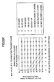
- Table 1 shows the configuration of the polarization beam splitter according to practical example 1.
- Layer 1 indicates a pair of transparent substrates and dielectric films.
- Substrate at the top part of Table 1 corresponds to the transparent substrate 11 shown in FIG. 1 .
- Substrate at the bottom part of Table 1 corresponds to the transparent substrate 12 shown in FIG. 1 .
- the numeric values 1 through 46 in the layer field (hereinafter, “layer number 1 through 46") indicate the order in which the dielectric films and an adhesive layer are deposited.
- “Substance” indicates materials of the transparent substrates and the dielectric films.
- Center wavelength indicates the design basis wavelength described above.
- Refractive index indicates the refractive index of the transparent substrates and the dielectric films.
- Frm thickness indicates, for each of the dielectric films, the product of the refractive index of a film and the physical thickness of the film itself, which corresponds to the optical thickness described above.
- Physical film thickness indicates the aforementioned thickness of the film itself.
- the mixture ratio of Nb 2 O 5 and SiO 2 in the mixture of the film Nb2O5/SiO2 is set in such a manner as to realize a refraction index of 1.572.
- the dielectric film of layer number 1 corresponds to one of two mid refractive index films between which the dielectric multilayer films are sandwiched (hereinafter, "sandwich-use mid refractive index films").
- the high refractive index film and the mid refractive index film are alternately laminated to form 14 layers in the second multilayer film.
- the third multilayer film is on the side of an adhesive layer (layer number 46).
- each of the two transparent substrates, between which the first through third multilayer films are sandwiched is a trapezoid.
- Each of the base angles of these trapezoids is set to be 60 degrees.
- the incident light LI is applied to the transparent substrate 11 from a side of the transparent substrate, in such a manner as to be incident on the polarization split film at an incidence angle of 60 degrees.
- polarization-splitting is performed at a wavelength region centering around 427 nm by the first multilayer film, at a wavelength region centering around 581 nm by the second multilayer film, and at a wavelength region centering around 658 nm by the third multilayer film.
- a favorable polarization-splitting function can be attained in a wavelength region ranging between 380 nm and 780 nm.
- the polarization beam splitter according to practical example 1 uses an inexpensive material for the transparent substrate, and has a small number of layers (45 layers). Therefore, time and cost required for deposition can be reduced. Accordingly, the polarization beam splitter can be manufactured at low cost, and can exhibit a favorable polarization-splitting function in a wide visible wavelength region.
- FIG. 4A illustrates the transmittance of P polarization (curve 4-1) and the transmittance of S polarization (curve 4-2) of modification 1.
- the transmittance of P polarization is 80% or more in a wavelength range of 360 nm through 800 nm and the transmittance of S polarization is substantially 0% in a wavelength range of 400 nm through 800 nm, which is a favorable polarization-splitting function.
- FIG. 4B illustrates the transmittance of P polarization (curve 4-3) and the transmittance of S polarization (curve 4-4) of modification 2.
- the transmittance of P polarization is 80% or more in a wavelength range of 350 nm through 800 nm and the transmittance of S polarization is substantially 0% in a wavelength range of 350 nm through 750 nm, which is a favorable polarization-splitting function.
- the mid refractive index films (a film made of a mixture of Nb 2 O 5 and SiO 2 ) have a refraction index of 1.72.
- FIG. 6A illustrates the transmittance of P polarization (curve 6-1) and the transmittance of S polarization (curve 6-2) of modification 5.
- the transmittance of P polarization is 95% or more in a wavelength range of 350 nm through 800 nm and the transmittance of S polarization is 5% or less in a wavelength range of 400 nm through 750 nm, which is a sufficient polarization-splitting function for practical use.
- the high refractive index film (a film made of Nb 2 O 5 ) has a refraction index of 2.336.
- Each refraction index of 2.086 for the high refractive index films in modification 5 and the refraction index of 2.236 for the high refractive index films in modification 6 is a central value at the wavelength of 550 nm.
- the values at actual center wavelengths of 610 nm, 830 nm, and 940 nm are 2.063, 2.020, and 2.009 in modification 5, and 2.313, 2.271, and 2.259 in modification 6, respectively.
- the configurations of the first through third multilayer films are the same as those of practical example 1, and the refractive index of the sandwich-use mid refractive index films (layer numbers 1 and 45) is changed.
- the sandwich-use mid refractive index films (a film made of a mixture of Nb 2 O 5 and SiO 2 ) has a refraction index of 1.555.
- the sandwich-use mid refractive index films (a film made of a mixture of Nb 2 O 5 and SiO 2 ) has a refraction index of 1.65.
- FIG. 7B illustrates the transmittance of P polarization (curve 7-3) and the transmittance of S polarization (curve 7-4) of modification 8.
- the transmittance of P polarization is 95% or more in a wavelength range of 400 nm through 800 nm and the transmittance of S polarization is substantially 0% in a wavelength range of 390 nm through 780 nm, which is a sufficient polarization-splitting function.
- Each refraction index of 1.555 for the sandwich-use mid refractive index films in modification 7 and the refraction index of 1.65 for the sandwich-use mid refractive index film in modification 8 is a central value at the wavelength of 550 nm.
- the values at actual center wavelengths of 610 nm, 830 nm, and 940 nm are 1.547, 1.527, and 1.521 in modification 7, and 1.641, 1.623, and 1.616 in modification 8, respectively.
- the sandwich-use mid refractive index films (layer numbers 1 and 45) included in practical example 1, between which the multilayer films are sandwiched, are not included in a polarization beam splitter of modification 9.
- FIG. 8 illustrates the transmittance of P polarization (curve 8-1) and the transmittance of S polarization (curve 8-2) of modification 9.
- the transmittance of P polarization is 95% or more in a wavelength range of 380 nm through 800 nm and the transmittance of S polarization is substantially 0% in a wavelength range of 400 nm through 780 nm, which is a sufficient polarization-splitting function.
- the transmittance of P polarization is 97% or more in the wavelength range of 380 nm through 800 nm in practical example 1 ( FIG. 2 ).
- the transmittance of P polarization is finely vibrating in the range surrounded by a square frame in FIG. 8 , i.e., in the wavelength range of 400 nm through 800 nm.
- the following describes the polarization splitting properties in a case where one more of the first through third multilayer films is employed.
- the first multilayer film including 14 layers corresponding to layer numbers 2 through 15 of practical example 1.
- a dielectric film as the single-layer dielectric film having the same configuration and thickness as the dielectric film corresponding to layer number 2 (center wavelength 610 nm, substance: Nb 2 O 5 , refractive index 2.213, physical film thickness: 68.90 nm), thereby forming 16 layers.
- sandwich-use mid refractive index film which is the same as that of layer number 1, thereby forming a polarization split film with a total of 17 layers.
- the sandwich-use mid refractive index film deposited last is adhered to the other substrate (substrate at bottom of Table 1) with the adhesive layer.
- FIG. 9 illustrates the transmittance of P polarization (curve 9-1) and the transmittance of S polarization (curve 9-2) in the aforementioned case.
- a favorable polarization-splitting function is attained at a wavelength region centering around 427 nm.
- the third multilayer film including 14 layers corresponding layer numbers 30 through 43 of practical example 1.
- a dielectric film as the single-layer dielectric film that is the same as the dielectric film corresponding to layer number 30 of practical example 1 (center wavelength 940 nm, substance: Nb 2 O 5 , refractive index 2.159, physical film thickness: 108.80 nm), thereby forming 16 layers.
- Table 4 shows this configuration, in accordance with Table 1.
- Table 4 CENTER WAVELENGTH ⁇ 0 REFRACTIVE INDEX n FILM THICKNESS nd PHYSICAL FILM THICKNESS d(nm) LAYER SUBSTANCE SUBSTRATE BSC7 - - - - 1 Nb2O5/SiO2 840.0 1.572 0.25 ⁇ 133.60 THIRD MULTILAYER FILM 2 Nb205 940.0 2.159 0.25 ⁇ 108.80 3 Nb2O5/SiO2 940.0 1.616 0.25 ⁇ 145.40 4 Nb205 940.0 2.159 0.25 ⁇ 108.80 5 Nb2O5/SiO2 940.0 1.616 0.25 ⁇ 145.40 6 Nb205 940.0 2.159 0.25 ⁇ 108.80 7 Nb2O5/SiO2 940.0 1.616 0.25 ⁇ 145.40 8 Nb2O5
- the wavelength region in which polarization-splitting can be performed is 400 nm through 650 nm, which is slightly narrower than the wavelength range of 380 nm through 780 nm of practical example 1. Nevertheless, this wavelength region (400 nm through 650 nm) substantially covers the visible wavelength region, and can thus tolerate practical use as a polarization beam splitter.
- Layer numbers 2 through 29 in Table 6 correspond to layer numbers 16 through 43 in practical example 1.
- the polarization-splitting properties in this case correspond to products of polarization-splitting properties of FIG. 10 and FIG. 11 .
- the transmittance of P polarization (curve 13-1) is favorable, but the transmittance of S polarization (curve 13-2) becomes large in a short wavelength region of 400 nm through 530 nm.
- a polarization-splitting function cannot be realized over the entire visible wavelength region.
- the polarization beam splitter can be favorably used as a polarization color filter that separates a green color component from visible light.
- the number of laminated layers included in each of the dielectric multilayer films in the polarization split film of the polarization beam splitter according to an embodiment of the present invention is 8 through 20, preferably 12 through 16.
- the number of laminated layers of dielectric films in each dielectric multilayer film is 14. In modification 11, the number laminated layers of dielectric films is 12. In modification 12, the number laminated layers of dielectric films is 10.
- the same number of laminated layers is provided in each of the dielectric multilayer films corresponding to different design basis wavelengths.
- the wavelength range is based on the entire visible region (400 nm through 700 nm).
- the effective wavelength range is 420 nm through 680 nm
- the transmittance of S polarization is less than 5% (the same as the case where there are eight laminated layers as described above), and that there can be any number of laminated layers in each basis wavelength. Accordingly, the total number of layers can be further reduced.
- the performance of the polarization beam splitter will be degraded.
- the limit at which the polarization beam splitter can tolerate practical use may vary according to required specifications of the system to be used, and therefore such a limit cannot be generalized.
- the limit of the transmittance of S polarization is around 10% (around 3% on average) in a wavelength range of 420 nm through 680 nm
- the number of laminated layers can be reduced to six layers in the first multilayer film and eight layers in the second and third multilayer films added together (i.e., the total of the number of laminated layers in the second multilayer film and the number of laminated layers in the third multilayer film).
- the first multilayer film of practical example 1 has six layers in modification 14
- the second multilayer film of practical example 1 has six layers in modification 14
- the third multilayer film of practical example 1 has two layers in modification 14.
- Table 8 shows this configuration, in accordance with Table 1. (Table 8) CENTER WAVELENGTH ⁇ 0 REFRACTIVE INDEX n FILM THICKNESS nd PHYSICAL FILMTHICKNESS d(nm) LAYER SUBSTANCE SUBSTRATE BSC7 - - - - 1 Nb2O5/SiO2 840.0 1.572 0.25 ⁇ 133.60 FIRST MULTILAYER FILM 2 Nb205 610.0 2.213 0.25 ⁇ 68.90 3 Nb2O5/SiO2 610.0 1.613 0.25 ⁇ 94.60 4 Nb205 610.0 2.213 0.25 ⁇ 68.90 5 Nb2O5/SiO2 610.0 1.613 0.25 ⁇ 94.60 6 Nb2O5 610.0 2.213 0.25 ⁇ 68.90 7 Nb2O5/SiO2 610.0 1.613 0.25 ⁇ 94.60 SECOND MUL
- a polarization beam splitter applicable to a system including a light source that has a limited wavelength region such as an LED used for illumination, it is not necessary to attain favorable properties across the entire visible region. It is satisfactory as long as favorable properties are attained in a wavelength region corresponding to the wavelength of the LED to be used. Accordingly, practical use will not be hampered by reducing the number of laminated layers in each multilayer film of the polarization beam splitter, as long as favorable properties of the polarization splitting function can be attained in the wavelength region that is actually necessary.
- the mixture layer of Nb 2 O 5 and SiO 2 acting as the mid refractive index film included in the polarization beam splitter may occur in a certain wavelength region depending on the deposition conditions.
- properties of the polarization beam splitter may be degraded.
- by reducing the number of mid refractive index films that cause such absorption it is possible to mitigate the extent of degradation in corresponding properties.
- FIG. 19 is a chart for comparing properties of the polarization beam splitter according to practical example 1 (having a combination of 14 layers, 14 layers, and 14 layers) and the polarization beam splitter according to modification 13 (having a combination of eight layers, six layers, and four layers), when absorption occurs in the films.
- FIGS. 20A through 20F are charts plotting the maximum values (hereinafter, "max values") of the transmittance of S polarization with respect to different combinations of numbers of laminated layers included in respective ones of the first multilayer film through the third multilayer film.
- the number of laminated layers in "the second multilayer film + the third multilayer film” is to be at least six layers (when the first multilayer film includes six layers or eight layers as in FIGS. 20E and 20D , respectively).
- the number of laminated layers in "the second multilayer film + the third multilayer film” is to be at least 10 layers.
- An S polarization transmittance of 5% can be attained when the first multilayer film includes eight layers ( FIG. 20D ) and "the second multilayer film + the third multilayer film” includes eight layers (six layers in the second multilayer film and two layers in the third multilayer film).
- S polarization transmittance of 5% or less it is considered that 10 layers are to be included in "the second multilayer film + the third multilayer film”.
- the minimum numbers of layers in each of the multilayer films are to be as follows: the first multilayer film includes six layers and "the second multilayer film + the third multilayer film” includes six layers; or the first multilayer film includes eight layers and "the second multilayer film + the third multilayer film” includes 10 layers.
- the performance will be further enhanced. Therefore, theoretically, there is no such thing as an upper limit in the number of laminated layers in consideration of performance. However, if there is an enormously vast number of laminated layers (such as over 100 layers), the actual performance may be degraded due to absorption. As a matter of practicality, the required minimum number of laminated layers is to be deposited in consideration of manufacturing efficiency and cost. Accordingly, it is meaningless to set an upper limit; there is significance in setting the aforementioned lower limit. Furthermore, the lower limit in the number of laminated layers is not limited to the above, because under actual circumstances, there may be irregularities in the device or materials when depositing the layers. Therefore, there needs to be freedom for increasing the number of laminated layers, in order to stably attain desirable performance.
- the sandwich-use mid refractive index film, the first through third multilayer films, and the single-layer film are formed and laminated starting from the side of the transparent substrate 11 in FIG. 1 .
- the sandwich-use mid refractive index film formed last (layer number 45) is adhered to the other transparent substrate by an adhesive layer (layer number 46).
- layer number 45 is adhered to the other transparent substrate by an adhesive layer
- layer number 46 is adhered to the sandwich-use mid refractive index film of layer number 1 from the other transparent substrate (in an order starting from layer number 45 toward layer number 1), and the sandwich-use mid refractive index film of layer number 1 can be adhered to the top transparent substrate by an adhesive layer.
- the dielectric films corresponding to layer numbers 44 through 31 of practical example 1 are included in the first multilayer film.
- the dielectric films corresponding to layer numbers 30 through 17 of practical example 1 are included in the second multilayer film.
- the dielectric films corresponding to layer numbers 16 through 3 of practical example 1 are included in the third multilayer film.
- the dielectric film corresponding to layer number 2 of practical example 1 acts as the single-layer dielectric film.
- FIG. 16A illustrates a polarization conversion element according to an embodiment of the present invention.
- the polarization conversion element shown in FIG. 16A is an optical element for receiving the incident light LI, which is natural light or light in a random polarization state, and emitting light beams having common polarization directions.
- Reference letters IS denote an incidence surface
- the incident light LI is orthogonally incident on the incidence surface IS.
- Reference letters OS denote an exit surface.
- the incidence surface IS and the exit surface OS are parallel to each other.
- reference numeral 20 indicate transparent substrates
- reference letter M denotes polarization split films (specifically, the polarization split film M includes at least two or more types of dielectric multilayer films, a single-layer dielectric film, and an adhesive layer, which are sandwiched between sandwich-use mid refractive index films as described in practical example 1 and modification examples 3 to 8 and 11 to 13).
- the plural polarization split films M are equidistant and parallel to each other, thereby constituting a polarization split film array.
- Each transparent substrate 20 is provided between and shared by two adjacent polarization split films M.
- each polarization split film M is formed by being deposited on one of the two transparent substrates 20 between which the polarization split film M is sandwiched, and is adhered to the other transparent substrate 20 by an adhesive layer. That is, the polarization split film array, which includes the polarization split films M and the transparent substrates 20 provided in between the polarization split films M, form a configuration in which multiple tiers of polarization beam splitters according to any of the above-described examples are stacked onto each other, thereby forming a combined single body.
- the shared transparent substrates 20 are cut along planes that are parallel to each other to form cut surfaces, each cut surface being at an angle of 60 degrees relative to the polarization split films M.
- the cut surfaces act as the incidence surface IS and the exit surface OS.
- the polarization split films M included in the polarization split film array are closely arranged to each other when viewed from directions orthogonal to the aforementioned cut surfaces (incidence surface/exit surface) (from the top and bottom directions when viewed in the figure).
- the incident light LI (described as collimated light beams as a matter of simplification) is applied to the polarization conversion element as shown in the figure, the incident light LI is incident on each polarization split film M at an incidence angle of 60 degrees.
- the above-described P polarization component passes through each polarization split film M as a transmitted light beam LT.
- the S polarization component is reflected from each polarization split film M.
- the reflected S polarization component propagates through the transparent substrate 20, and is reflected once again from an adjacent polarization split film M, which is, when viewed in the figure, on the immediate right of the polarization split film M from which the S polarization component is first reflected.
- each 1/2 wavelength plate 30 On the exit surface OS of the polarization conversion element, there are provided equidistant 1/2 wavelength plates 30, each having a rectangular shape that is elongated in the direction orthogonal to the figure. Each 1/2 wavelength plate 30 is configured to spin around the polarization plane of the transmitted light beam LT by 90 degrees.
- the polarization plane of the transmitted light beam LT that has transmitted through the polarization split film M is spun around by 90 degrees by the 1/2 wavelength plate 30; however, the present invention is not limited thereto.
- the reflected light beam LR that has been reflected from the polarization split film M can be incident on the 1/2 wavelength plate 30 so that its polarization plane is spun around by 90 degrees in such a manner as to be in the same direction as that of the transmitted light beam LT.
- FIG. 16B illustrates a conventional polarization conversion element, in which a polarization split film M1 and a reflection film R1 are tilted by 45 degrees relative to the incidence surface IS and the exit surface OS, and are alternately arranged with transparent substrates 21 interposed therebetween.
- the incident light LI incident on the polarization split film M1 which is natural light or light in a random polarization state, undergoes polarization splitting according to respective polarization components, and is split into a transmitted light beam LT and a reflected light beam LR.
- the reflected light beam LR is reflected from the reflection film R1 adjacent to the polarization split film M1, and its polarization plane is spun around by 90 degrees by the 1/2 wavelength plate 30 in such a manner as to be in the same direction as that of the transmitted light beam LT. Accordingly, the polarization planes of the output light beams are made to be in the same direction.
- the polarization conversion element according to an embodiment of the present invention does not require the reflection film R1. For this reason, the polarization conversion element according to an embodiment of the present invention only requires half as many laminated layers of transparent substrates as that of the conventional polarization conversion element, and thus has a simple configuration and has advantageous manufacturability.
- a polarization beam splitter for polarization-splitting incident light is provided.
- the polarization beam splitter is effective when light to undergo polarization-splitting has an incidence angle that falls in a range of 54 degrees through 66 degrees.
- the best polarization splitting properties can be attained when the incidence angle is around 54 degrees through 60 degrees.
- An embodiment of the present invention effectively utilizes this fact. That is, the polarization beam splitter according to an embodiment of the present invention is effective, i.e., has favorable polarization splitting properties, with respect to light incident at an incident angle range near Brewster's conditions.
- the polarization beam splitter includes a pair of transparent substrates, and between the pair of transparent substrates are sandwiched an adhesive layer, two or more types of dielectric multilayer films, and a single-layer dielectric film.
- the adhesive layer is for adhering to a. first transparent substrate of the two transparent substrates.
- the two or more types of dielectric multilayer films have different design basis wavelengths.
- Each of the two or more types of dielectric multilayer films includes high refractive index films and mid refractive index films each having an optical thickness in accordance with the corresponding design basis wavelength.
- the high refractive index films and the mid refractive index films are alternately laminated to form an even number of layers. Because an even number of laminated layers are formed in each dielectric multilayer film, one of the dielectric films at the ends of each dielectric multilayer film is a high refractive index film and the other one is a mid refractive index film.
- the two or more types of dielectric multilayer films and the single-layer dielectric film form a polarization split film, which performs a polarization split function with respect to light that substantially includes the visible wavelength region.
- the two or more types of dielectric multilayer films are formed by sequentially depositing and laminating layers on one of the two transparent substrates. On top of the dielectric multiyear film formed last, the single-layer dielectric film is deposited.
- the single-layer dielectric film has the same composition and thickness as one of the films corresponding to a first layer in the dielectric multilayer film formed last.
- the incidence angle corresponds to the angle at the incidence surface of the incident transparent substrate. Accordingly, if the incidence angle is set to be, for example 54 degrees for light applied to an incidence surface, which is the side surface (the oblique surface) of the incident transparent substrate having a trapezoidal cross-sectional shape with base angles of 60 degrees, the incidence angle at the polarization split film will be less than 54 degrees according to the function of refraction of the transparent substrate.
- each of the sandwich-use mid refractive index films is made of a mixture of Nb 2 O 5 and SiO 2 and has a different refractive index from those of the mid refractive index films in the dielectric multilayer films.
- An optical thickness of each of the sandwich-use mid refractive index films is set to be ⁇ /4 with respect to a wavelength ⁇ that is different from any of the design basis wavelengths of the two or more types of dielectric multilayer films.
- the numbers of layers in the three types of dielectric multilayer films can be changed.
- optical thickness of each of the high refractive index films, the mid refractive index films, and the sandwich-use mid refractive index films corresponds to the product of the thickness of the film itself (physical thickness) and the refractive index of the film component.
- the high refractive index films are made of Nb 2 O 5 and the mid refractive index films are made of a mixture of Nb 2 O 5 and SiO 2 .
- the high refractive index films are deposited by performing Nb reactive sputtering.
- the mid refractive index films are deposited by simultaneously performing Si reactive sputtering and Nb reactive sputtering.
- the refractive index of the mid refractive index film can be adjusted by adjusting the magnitude relationship of the intensity of Si sputtering and the intensity of Nb sputtering when Si reactive sputtering and Nb reactive sputtering are simultaneously performed to form the mid refractive index film.
- Nb 2 O 5 has a high refractive index of around 2.34 and SiO 2 has a low refractive index of around 1.43.
- the mid refractive index film is adjusted to literally have a mid refractive index (e.g., around 1.56 through 1.75).
- a mid refractive index e.g., around 1.56 through 1.75.
- the components in the actually deposited high refractive index film are not purely Nb 2 O 5 , but a small amount of the different type of substance may be incorporated. Furthermore, the filling density of the film is irregular. Therefore, the refractive index of the high refractive index film made of Nb 2 O 5 changes in a range of around 2.07 through 2.34. However, by adjusting the depositing conditions to attain a constant refractive index, the refractive index of the high refractive index film can be controlled to be at a constant level with favorable reproducibility. Accordingly, such a different type of substance will not have adverse effects on the high refractive index film.
- the pair of transparent substrates is made of BK7.
- a polarization conversion element includes a plurality of any of the above-described polarization beam splitters stacked in multiple tiers, thereby forming a polarization split film array.
- the polarization split films that are parallel and adjacent to each other share a common one of the transparent substrates.
- the shared transparent substrates are cut along planes that are parallel to each other to form cut surfaces, each of the cut surfaces being at an angle of substantially 60 degrees relative to the polarization split films.
- the polarization split films parallel to each other are provided in close contact to or near each other when viewed from directions orthogonal to the cut surfaces. Incident light to undergo polarization-splitting is applied to the polarization split film array from one of the cut surfaces acting as an incidence surface.
- the incident light is split into transmitted light and reflected light at each of the polarization split films according to respective polarization components, and the reflected light is reflected from an adjacent one of the polarization split films, in such a manner that light, which exits at another one of the cut surfaces acting as an exist surface, propagates in the same direction as that of the incident light.
- One-half wavelength plates are provided on the other one of the cut surfaces acting as the exit surface at portions from which the transmitted light or the reflected light exit, thereby attaining light having a single polarization state.
- all of the polarization split films are tilted by 60 degrees relative to at least one of the incidence surface and the exit surface, and the polarization split films are provided in close contact to each other when viewed from at least one of an incidence direction and an exit direction.
Claims (7)
- Séparateur de faisceau polarisant (10) pour la séparation de polarisation de la lumière incidente, où le séparateur de faisceau polarisant est efficace lorsque la lumière devant faire l'objet de la séparation de polarisation, a un angle d'incidence qui tombe dans une plage de 54 degrés à 66 degrés, le séparateur de faisceau polarisant comprenant, entre deux substrats transparents (11, 12) de BK7 chacun ayant une forme de coupe transversale trapézoïdale, l'angle de base de chaque trapézoïde étant de 60 degrés:une couche adhésive (14) collée à un premier substrat transparent (12) des deux substrats transparents;un premier, un deuxième et un troisième films diélectriques multicouches (13) ayant des longueurs d'onde de base calculées de 610, 830 et 940 nm respectivement, la longueur d'onde de base calculée étant la même pour toutes les couches de chaque film multicouche, formées sur le deuxième substrat transparent (11); etun film diélectrique monocouche d'un quart de longueur d'onde en Nb2O5 avec une longueur d'onde centrale de 940 nm, formé entre la couche adhésive (4) et les films diélectriques multicouches (13), dans lequel:chacun des films diélectriques multicouches comprend des films en Nb2O5 d'un quart de longueur d'onde à haut indice de réfraction et des films d'un quart de longueur d'onde à indice de réfraction moyen en un mélange de Nb2O5 et de SiO2, où les films à haut indice de réfraction et les films à indice de réfraction moyen sont stratifiés d'une manière alternée pour former un nombre pair de couches;les films diélectriques multicouches et le film diélectrique monocouche forment un film séparateur de polarisation qui remplit une fonction de séparation de polarisation pour la lumière qui est sensiblement dans la région de longueur d'onde visible; etles films diélectriques multicouches et le film diélectrique monocouche sont en sandwich entre deux films d'un quart de longueur d'onde à indice de réfraction moyen en un mélange de Nb2O5 et de SiO2 de formation de sandwich, lesquels ont un indice de réfraction différent de ceux des films à indice de réfraction moyen dans les films diélectriques multicouches et une longueur d'onde centrale de 840 nm;où le séparateur de faisceau polarisant est agencé pour effectuer la séparation de polarisation soit: (a) à des régions de longueurs d'onde centrées autour de 427 nm, 581 nm et 658 nm, par le premier, le deuxième et le troisième films multicouches respectivement, avec un facteur de transmission de polarisation P de 95% ou plus et un facteur de transmission de polarisation S sensiblement de 0% dans la plage de longueurs d'onde de 380 nm à 780 nm, soit (b) avec un facteur de transmission de polarisation P de 98% ou plus et de 99% ou plus en moyenne et un facteur de transmission de polarisation S de 3% ou moins et de 1% ou moins en moyenne dans la plage de longueurs d'onde de 420 nm à 680 nm, soit (c) avec un facteur de transmission de polarisation P de 98% ou plus et de 99% ou plus en moyenne et un facteur de transmission de polarisation S de 10% ou moins et d'environ 3% ou moins en moyenne dans la plage de longueurs d'onde de 420 nm à 680 nm.
- Séparateur de faisceau polarisant selon la revendication 1, dans lequel il y a 14 dites couches dans chaque film diélectrique multicouche (13) et le séparateur de faisceau polarisant est agencé pour effectuer la séparation de polarisation avec un facteur de transmission de polarisation P de 95% ou plus et un facteur de transmission de polarisation S sensiblement de 0% dans la plage de longueurs d'onde de 380 nm à 780 nm.
- Séparateur de faisceau polarisant selon la revendication 1, dans lequel il y a 8 dites couches dans le premier film multicouche, 6 dites couches dans le deuxième film multicouche et 4 dites couches dans le troisième film multicouche et le séparateur de faisceau polarisant est agencé pour effectuer la séparation de polarisation avec un facteur de transmission de polarisation P de 98% ou plus et de 99% ou plus en moyenne et un facteur de transmission de polarisation S de 3% ou moins et de 1% ou moins en moyenne dans la plage de longueurs d'onde de 420 nm à 680 nm.
- Séparateur de faisceau polarisant selon la revendication 1, dans lequel il y a 6 dites couches dans le premier film multicouche, 6 dites couches dans le deuxième film multicouche et 2 dites couches dans le troisième film multicouche et le séparateur de faisceau polarisant est agencé pour effectuer la séparation de polarisation avec un facteur de transmission de polarisation P de 98% ou plus et de 99% ou plus en moyenne et un facteur de transmission de polarisation S de 10% ou moins et d'environ 3% ou moins en moyenne dans la plage de longueurs d'onde de 420 nm à 680 nm.
- Séparateur de faisceau polarisant selon l'une quelconque des revendications précédentes, dans lequel l'indice de réfraction de chacun des films à indice de réfraction moyen est établi par un rapport du mélange de Nb2O5 et de SiO2.
- Elément de conversion de polarisation comprenant plusieurs séparateurs de faisceau polarisants selon l'une quelconque des revendications précédentes, empilés en des étages multiples formant un ensemble de films séparateurs de polarisation;
dans lequel les films séparateurs de polarisation qui sont parallèles et adjacents les uns aux autres partagent un substrat commun des substrats transparents;
les substrats transparents partagés sont coupés le long de plans qui sont parallèles les uns aux autres pour former des surfaces coupées, chacune des surfaces coupées étant à un angle sensiblement de 60 degrés par rapport aux films séparateurs de polarisation;
les films séparateurs de polarisation parallèles les uns aux autres sont fournis en étroit contact les uns avec les autres ou près les uns des autres lorsque vus de directions orthogonales aux surfaces coupées;
de sorte qu'en emploi, lorsque la lumière incidente devant faire l'objet de la séparation de polarisation est appliquée à l'ensemble de films séparateurs de polarisation de l'une des surfaces coupées agissant en tant que surface d'incidence, la lumière incidente est séparée en lumière transmise et lumière réfléchie au niveau de chacun des films séparateurs de polarisation conformément aux composants de polarisation respectifs et la lumière réfléchie est réfléchie d'un film adjacent des films séparateurs de polarisation d'une manière telle que la lumière, qui sort d'une autre des surfaces coupées agissant en tant que surface de sortie, se propage dans la même direction que celle de la lumière incidente; et dans lequel
des plaques d'une ½ longueur d'onde sont fournies sur ladite autre des surfaces coupées agissant en tant que surface de sortie, à des parties desquelles sort la lumière transmise ou la lumière réfléchie, réalisant ainsi une lumière ayant un seul état de polarisation. - Elément de conversion de polarisation selon la revendication 6, dans lequel:tous les films séparateurs de polarisation sont inclinés à 60 degrés par rapport à au moins l'une des surfaces d'incidence et de la surface de sortie; etles films séparateurs de polarisation sont fournis en étroit contact les uns avec les autres lorsque vus d'au moins l'une d'une direction d'incidence et d'une direction de sortie.
Applications Claiming Priority (2)
| Application Number | Priority Date | Filing Date | Title |
|---|---|---|---|
| JP2006356390 | 2006-12-28 | ||
| JP2007266540A JP5209932B2 (ja) | 2006-12-28 | 2007-10-12 | 偏光ビームスプリッタおよび偏光変換素子 |
Publications (3)
| Publication Number | Publication Date |
|---|---|
| EP1939655A2 EP1939655A2 (fr) | 2008-07-02 |
| EP1939655A3 EP1939655A3 (fr) | 2010-06-09 |
| EP1939655B1 true EP1939655B1 (fr) | 2013-07-17 |
Family
ID=39144294
Family Applications (1)
| Application Number | Title | Priority Date | Filing Date |
|---|---|---|---|
| EP07254969.4A Expired - Fee Related EP1939655B1 (fr) | 2006-12-28 | 2007-12-20 | Séparateur de faisceau de polarisation et élément de conversion de polarisation |
Country Status (2)
| Country | Link |
|---|---|
| US (1) | US7961392B2 (fr) |
| EP (1) | EP1939655B1 (fr) |
Families Citing this family (8)
| Publication number | Priority date | Publication date | Assignee | Title |
|---|---|---|---|---|
| JP4574439B2 (ja) * | 2004-08-09 | 2010-11-04 | キヤノン株式会社 | 偏光分離素子及びそれを有する投影装置 |
| US8958156B1 (en) | 2007-05-30 | 2015-02-17 | Semrock, Inc. | Interference filter for non-zero angle of incidence spectroscopy |
| JP2009169279A (ja) * | 2008-01-18 | 2009-07-30 | Nitto Denko Corp | 偏光板およびそれを用いた画像表示装置 |
| US8817371B1 (en) | 2008-08-01 | 2014-08-26 | Simon Andrew Boothroyd | Polarizing beam splitters |
| US8879150B1 (en) * | 2009-03-20 | 2014-11-04 | Semrock, Inc. | Optical thin-film polarizing bandpass filter |
| US9188790B2 (en) * | 2010-05-21 | 2015-11-17 | 3M Innovative Properties Company | Partially reflecting multilayer optical films with reduced color |
| CN103207427A (zh) * | 2013-04-03 | 2013-07-17 | 中国科学院上海光学精密机械研究所 | 双折射薄膜反射式位相延迟片 |
| US11733534B2 (en) | 2021-01-21 | 2023-08-22 | AdlOptica Optical Systems GmbH | Optics for formation of multiple light spots with controlled spot intensity and variable spot pattern geometry |
Citations (1)
| Publication number | Priority date | Publication date | Assignee | Title |
|---|---|---|---|---|
| US5453859A (en) * | 1993-06-03 | 1995-09-26 | Matsushita Electric Industrial Co., Ltd. | Polarization beam splitter and projection display apparatus |
Family Cites Families (11)
| Publication number | Priority date | Publication date | Assignee | Title |
|---|---|---|---|---|
| TW401530B (en) * | 1996-03-12 | 2000-08-11 | Seiko Epson Corp | Polarized light separation device, method of fabricating the same and projection display apparatus using the polarized light separation device |
| US6351296B1 (en) * | 1998-01-27 | 2002-02-26 | Fabia Engineering (1992) Ltd. | Liquid crystal beam polarizer and method for manufacturing thereof |
| JPH11211916A (ja) | 1998-01-27 | 1999-08-06 | Nikon Corp | 偏光ビームスプリッター |
| JP3633376B2 (ja) * | 1999-06-21 | 2005-03-30 | セイコーエプソン株式会社 | 偏光分離装置の製造方法 |
| JP2002207120A (ja) * | 2001-01-05 | 2002-07-26 | Nikon Corp | 偏光ビームスプリッタ、投射型表示装置用光学装置、投射型表示装置及び偏光ビームスプリッタの製造方法 |
| JP4200266B2 (ja) | 2002-04-01 | 2008-12-24 | パナソニック株式会社 | ダイクロイックミラー及び投写型表示装置 |
| JP3812527B2 (ja) * | 2002-09-26 | 2006-08-23 | コニカミノルタオプト株式会社 | 偏光ビームスプリッタ |
| DE10247004A1 (de) | 2002-10-09 | 2004-04-22 | Deutsche Telekom Ag | Polarisator für Licht sowie Verfahren zum Herstellen eines solchen |
| US6870676B2 (en) * | 2003-01-27 | 2005-03-22 | Daniel Lee Stark | Layered micro optics polarization converter |
| JP2005107317A (ja) * | 2003-09-30 | 2005-04-21 | Minolta Co Ltd | 偏光分離膜および偏光分離プリズム |
| JP2007266540A (ja) | 2006-03-30 | 2007-10-11 | Elpida Memory Inc | 半導体装置及びその製造方法 |
-
2007
- 2007-12-20 US US11/961,611 patent/US7961392B2/en not_active Expired - Fee Related
- 2007-12-20 EP EP07254969.4A patent/EP1939655B1/fr not_active Expired - Fee Related
Patent Citations (1)
| Publication number | Priority date | Publication date | Assignee | Title |
|---|---|---|---|---|
| US5453859A (en) * | 1993-06-03 | 1995-09-26 | Matsushita Electric Industrial Co., Ltd. | Polarization beam splitter and projection display apparatus |
Also Published As
| Publication number | Publication date |
|---|---|
| EP1939655A2 (fr) | 2008-07-02 |
| US20080158673A1 (en) | 2008-07-03 |
| US7961392B2 (en) | 2011-06-14 |
| EP1939655A3 (fr) | 2010-06-09 |
Similar Documents
| Publication | Publication Date | Title |
|---|---|---|
| EP1939655B1 (fr) | Séparateur de faisceau de polarisation et élément de conversion de polarisation | |
| US5221982A (en) | Polarizing wavelength separator | |
| EP1820051B1 (fr) | Polariseur thermoelectrique multicouche | |
| US5061050A (en) | Polarizer | |
| EP1510838B1 (fr) | Séparateur de faisceaux polarisant, système optique et appareil de visualisation l'utilisant | |
| US8817371B1 (en) | Polarizing beam splitters | |
| US20070121210A1 (en) | Polarized diffractive filter and layered polarized diffractive filter | |
| KR100825905B1 (ko) | 액정표시장치 | |
| US7012747B2 (en) | Polarizing beam splitter and polarizer using the same | |
| JP2002169026A (ja) | コリメータ及びバックライトシステム | |
| JP5209932B2 (ja) | 偏光ビームスプリッタおよび偏光変換素子 | |
| KR20190009426A (ko) | 반사 편광기 및 보상 필름을 포함하는 광학 적층물 | |
| JP3584257B2 (ja) | 偏光ビームスプリッタ | |
| JPH11202127A (ja) | ダイクロイックミラー | |
| JP2003043460A (ja) | 液晶表示素子 | |
| KR101061521B1 (ko) | 파장 합분파기 | |
| JP2001350024A (ja) | 偏光ビームスプリッタ | |
| JPH04140714A (ja) | 可変波長フィルタモジュール | |
| JP4054623B2 (ja) | 光学多層膜及び光学素子 | |
| JPH08110406A (ja) | 光学多層膜 | |
| JP2012150510A (ja) | 反射型光変調装置 | |
| JP2003066231A (ja) | 偏光ビームスプリッタ | |
| JP4285032B2 (ja) | 偏光ビーム変換素子及びその製造方法、液晶表示装置 | |
| WO2020161950A1 (fr) | Diviseur de faisceau polarisé, et dispositif optique | |
| JPH05203811A (ja) | 偏光ビームスプリッター |
Legal Events
| Date | Code | Title | Description |
|---|---|---|---|
| PUAI | Public reference made under article 153(3) epc to a published international application that has entered the european phase |
Free format text: ORIGINAL CODE: 0009012 |
|
| 17P | Request for examination filed |
Effective date: 20080108 |
|
| AK | Designated contracting states |
Kind code of ref document: A2 Designated state(s): AT BE BG CH CY CZ DE DK EE ES FI FR GB GR HU IE IS IT LI LT LU LV MC MT NL PL PT RO SE SI SK TR |
|
| AX | Request for extension of the european patent |
Extension state: AL BA HR MK RS |
|
| PUAL | Search report despatched |
Free format text: ORIGINAL CODE: 0009013 |
|
| AK | Designated contracting states |
Kind code of ref document: A3 Designated state(s): AT BE BG CH CY CZ DE DK EE ES FI FR GB GR HU IE IS IT LI LT LU LV MC MT NL PL PT RO SE SI SK TR |
|
| AX | Request for extension of the european patent |
Extension state: AL BA HR MK RS |
|
| AKX | Designation fees paid |
Designated state(s): DE FR GB |
|
| 17Q | First examination report despatched |
Effective date: 20111215 |
|
| GRAP | Despatch of communication of intention to grant a patent |
Free format text: ORIGINAL CODE: EPIDOSNIGR1 |
|
| GRAS | Grant fee paid |
Free format text: ORIGINAL CODE: EPIDOSNIGR3 |
|
| GRAA | (expected) grant |
Free format text: ORIGINAL CODE: 0009210 |
|
| AK | Designated contracting states |
Kind code of ref document: B1 Designated state(s): DE FR GB |
|
| REG | Reference to a national code |
Ref country code: GB Ref legal event code: FG4D |
|
| REG | Reference to a national code |
Ref country code: DE Ref legal event code: R096 Ref document number: 602007031664 Country of ref document: DE Effective date: 20130912 |
|
| PGFP | Annual fee paid to national office [announced via postgrant information from national office to epo] |
Ref country code: GB Payment date: 20131219 Year of fee payment: 7 |
|
| PLBE | No opposition filed within time limit |
Free format text: ORIGINAL CODE: 0009261 |
|
| STAA | Information on the status of an ep patent application or granted ep patent |
Free format text: STATUS: NO OPPOSITION FILED WITHIN TIME LIMIT |
|
| PGFP | Annual fee paid to national office [announced via postgrant information from national office to epo] |
Ref country code: FR Payment date: 20131220 Year of fee payment: 7 |
|
| 26N | No opposition filed |
Effective date: 20140422 |
|
| REG | Reference to a national code |
Ref country code: DE Ref legal event code: R097 Ref document number: 602007031664 Country of ref document: DE Effective date: 20140422 |
|
| PGFP | Annual fee paid to national office [announced via postgrant information from national office to epo] |
Ref country code: DE Payment date: 20141211 Year of fee payment: 8 |
|
| GBPC | Gb: european patent ceased through non-payment of renewal fee |
Effective date: 20141220 |
|
| REG | Reference to a national code |
Ref country code: FR Ref legal event code: ST Effective date: 20150831 |
|
| PG25 | Lapsed in a contracting state [announced via postgrant information from national office to epo] |
Ref country code: GB Free format text: LAPSE BECAUSE OF NON-PAYMENT OF DUE FEES Effective date: 20141220 |
|
| PG25 | Lapsed in a contracting state [announced via postgrant information from national office to epo] |
Ref country code: FR Free format text: LAPSE BECAUSE OF NON-PAYMENT OF DUE FEES Effective date: 20141231 |
|
| REG | Reference to a national code |
Ref country code: DE Ref legal event code: R119 Ref document number: 602007031664 Country of ref document: DE |
|
| PG25 | Lapsed in a contracting state [announced via postgrant information from national office to epo] |
Ref country code: DE Free format text: LAPSE BECAUSE OF NON-PAYMENT OF DUE FEES Effective date: 20160701 |