EP1932803B1 - MEMS device with Z-axis asymetry - Google Patents
MEMS device with Z-axis asymetry Download PDFInfo
- Publication number
- EP1932803B1 EP1932803B1 EP07122530.4A EP07122530A EP1932803B1 EP 1932803 B1 EP1932803 B1 EP 1932803B1 EP 07122530 A EP07122530 A EP 07122530A EP 1932803 B1 EP1932803 B1 EP 1932803B1
- Authority
- EP
- European Patent Office
- Prior art keywords
- base
- comb
- gap
- comb structure
- planar
- Prior art date
- Legal status (The legal status is an assumption and is not a legal conclusion. Google has not performed a legal analysis and makes no representation as to the accuracy of the status listed.)
- Ceased
Links
Images
Classifications
-
- B—PERFORMING OPERATIONS; TRANSPORTING
- B81—MICROSTRUCTURAL TECHNOLOGY
- B81C—PROCESSES OR APPARATUS SPECIALLY ADAPTED FOR THE MANUFACTURE OR TREATMENT OF MICROSTRUCTURAL DEVICES OR SYSTEMS
- B81C1/00—Manufacture or treatment of devices or systems in or on a substrate
- B81C1/00015—Manufacture or treatment of devices or systems in or on a substrate for manufacturing microsystems
- B81C1/00134—Manufacture or treatment of devices or systems in or on a substrate for manufacturing microsystems comprising flexible or deformable structures
- B81C1/00182—Arrangements of deformable or non-deformable structures, e.g. membrane and cavity for use in a transducer
Definitions
- MEMS processing techniques create structures that are symmetric in the z axis (out of the wafer's surface) but can vary in the x and y axes (in the plane of the wafer's surface).
- creating asymmetry in the z-axis can be performed by deflecting with stiction plates or by selective thinning. Deflecting with stiction plates leads to devices which are sensitive to z motion, but is not easily implemented for multiple z-offsets in both the positive and negative z directions and also requires more steps and additional processing layers, thereby costing more money.
- Selective thinning is performed by thinning one set of teeth of a comb drive in the Z-direction, but this requires an extra mask and additional etches, and it is also rather inaccurate.
- One method of more easily creating asymmetry requires a top and a bottom cover enclosing the mechanism layer of the MEMS device to produce asymmetry in the negative and positive z directions.
- Some uses for MEMS devices require an exposed mechanism layer, and a top cover is incompatible with these uses.
- Article "Selective stiction based vertical comb actuators" by Jongbaeg Kim et al, discloses the application of a selective stiction process to provide interleaved, angularly displaced, electrostatic comb drive actuators. More specifically, an arrangement is shown in which two static combs are interleaved with a suspended, double sided comb structure wherein the suspended, double sided comb structure is suspended by a torsion bar which is anchored on one side at a height corresponding to the static combs, and anchored on the other side with a stiction plate which is stuck to a lower substrate. This disparity causes the torsion bar to twist, which in turn causes the angular displacement of the suspended, double sided comb structure relative to the corresponding static combs.
- MEMS microelectromechanical system
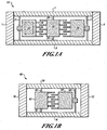
- FIGURE 1A is a top view of an example mechanism layer 12 formed according to the present invention.
- the mechanism layer 12 includes walls 5, 6, 7, 8, a first movable portion 14, a second movable portion 16, and a fixed portion 18.
- the first movable portion 14 is attached to walls 7, 8 by flexure 15 (also torsional flexure or hinge), the second movable portion 16 is attached to walls 7, 8 by flexure 17, and the fixed portion 18 is attached to walls 7, 8 by flexures 19.
- FIGURE 1B is a top view of an alternate embodiment of a mechanism layer 48.
- the mechanism layer 48 includes walls 50, 52, 54, 56, a movable portion 64 attached to walls 54, 56 by flexure 60, and a fixed portion 62 attached to walls 54, 56 by flexures 58.
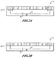
- FIGURES 2A, 2B , and 2C illustrate side views of various intermediate structures of a microelectromechanical system (MEMS) device 10 formed in accordance with one embodiment of the invention.
- FIGURE 2A shows the mechanism layer 12 of FIGURE 1A .
- the mechanism layer 12 is made of silicon.
- a base 20 with a top surface 21, a gap 22, and a gap surface 23 is also shown.
- the base 20 is made of glass.
- the depth of the gap 22 equals the desired z-offset distance of the fixed portion 18.
- the gap 22 is formed by wet etching or other processes known to those have ordinary skill in the art.
- FIGURE 2B shows the mechanism layer 12 and the base 20 after bonding the mechanism layer 12 to the top surface 21.
- anodic bonding may be used to bond the mechanism layer 12 to the top surface 21.
- the base 20 and mechanism layer 12 are made of different materials, appropriate bonding techniques known to those having ordinary skill in the art may be used.
- flexures 15 and 17 allow movement of the movable portions 14, 16.
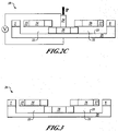
- FIGURE 2C shows the base 20 with the fixed portion 18 of the mechanism layer 12 being displaced down into contact with the gap surface 23 by an electrically conductive or semi-conductive material 24, preferably highly doped silicon.
- the electrically conductive material 24 is sized and shaped such that it may be used to displace the fixed portion 18 but not the first and second movable portions 14, 16. While the electrically conductive material 24 is in contact with the fixed portion 18 and the fixed portion 18 is in contact with the gap surface 23, a voltage V and a pressure P are applied between the base 20 and the fixed portion 18 to effect bonding of the fixed portion 18 to the gap surface 23. After bonding, the electrically conductive material 24 is removed, leaving the finished structure 26 of FIGURE 3 (note that walls 7, 8 are not shown for clarity).
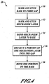
- FIGURE 4 A block diagram 28 of an example method according to the present invention is shown in FIGURE 4 .
- a base is masked and etched to form a gap.
- a mechanism layer is masked and etched to form the various structures of the mechanism layer.
- the mechanism layer is bonded to the base.
- a portion of the mechanism layer is deflected into the gap of the base until it contacts a surface of the gap.
- the deflected portion is bonded to the base.
- the method of the present invention may be combined with the methods disclosed in US patent 7516661 and titled "Z OFFSET MEMS DEVICE" to enable offsets in the positive and negative z directions without including a top cover. Offsets in the negative z direction can be produced by the methods of the present invention, and offsets in the positive z direction can be produced by the methods of US patent 7516661 .
Landscapes
- Engineering & Computer Science (AREA)
- Manufacturing & Machinery (AREA)
- Microelectronics & Electronic Packaging (AREA)
- Micromachines (AREA)
- Pressure Sensors (AREA)
- Analysing Materials By The Use Of Radiation (AREA)
Description
- Standard microelectromechanical systems (MEMS) processing techniques create structures that are symmetric in the z axis (out of the wafer's surface) but can vary in the x and y axes (in the plane of the wafer's surface). Presently, creating asymmetry in the z-axis can be performed by deflecting with stiction plates or by selective thinning. Deflecting with stiction plates leads to devices which are sensitive to z motion, but is not easily implemented for multiple z-offsets in both the positive and negative z directions and also requires more steps and additional processing layers, thereby costing more money. Selective thinning is performed by thinning one set of teeth of a comb drive in the Z-direction, but this requires an extra mask and additional etches, and it is also rather inaccurate. One method of more easily creating asymmetry requires a top and a bottom cover enclosing the mechanism layer of the MEMS device to produce asymmetry in the negative and positive z directions. Some uses for MEMS devices require an exposed mechanism layer, and a top cover is incompatible with these uses.
- Thus, there exists a need for methods to easily form z-offsets in MEMS devices without completely enclosing the MEMS device.
- Article "Selective stiction based vertical comb actuators" by Jongbaeg Kim et al, (ISBN 978-0-7803-8732-4) discloses the application of a selective stiction process to provide interleaved, angularly displaced, electrostatic comb drive actuators. More specifically, an arrangement is shown in which two static combs are interleaved with a suspended, double sided comb structure wherein the suspended, double sided comb structure is suspended by a torsion bar which is anchored on one side at a height corresponding to the static combs, and anchored on the other side with a stiction plate which is stuck to a lower substrate. This disparity causes the torsion bar to twist, which in turn causes the angular displacement of the suspended, double sided comb structure relative to the corresponding static combs.
- According to the present invention, there is provided a microelectromechanical system (MEMS) device and a corresponding method as claimed in any of the accompanying claims.
-
-
FIGURES 1A and 1B are top views of alternate embodiments of mechanism layers formed in accordance with the present invention; -
FIGURES 2A, 2B , and2C illustrate various intermediate structures produced by a method according to the present invention; -
FIGURE 3 is a side view of a MEMS device according to the present invention; and -
FIGURE 4 is a block diagram of a method according to the present invention. -
FIGURE 1A is a top view of anexample mechanism layer 12 formed according to the present invention. Themechanism layer 12 includeswalls movable portion 14, a secondmovable portion 16, and a fixedportion 18. The firstmovable portion 14 is attached towalls 7, 8 by flexure 15 (also torsional flexure or hinge), the secondmovable portion 16 is attached towalls 7, 8 byflexure 17, and thefixed portion 18 is attached towalls 7, 8 byflexures 19. -
FIGURE 1B is a top view of an alternate embodiment of amechanism layer 48. Themechanism layer 48 includeswalls walls fixed portion 62 attached towalls flexures 58. -
FIGURES 2A, 2B , and2C illustrate side views of various intermediate structures of a microelectromechanical system (MEMS)device 10 formed in accordance with one embodiment of the invention.FIGURE 2A shows themechanism layer 12 ofFIGURE 1A . Themechanism layer 12 is made of silicon. Abase 20 with atop surface 21, agap 22, and agap surface 23 is also shown. Thebase 20 is made of glass. The depth of thegap 22 equals the desired z-offset distance of thefixed portion 18. Thegap 22 is formed by wet etching or other processes known to those have ordinary skill in the art. -
FIGURE 2B shows themechanism layer 12 and thebase 20 after bonding themechanism layer 12 to thetop surface 21. In the case of asilicon mechanism layer 12 and aglass base 20, anodic bonding may be used to bond themechanism layer 12 to thetop surface 21. When thebase 20 andmechanism layer 12 are made of different materials, appropriate bonding techniques known to those having ordinary skill in the art may be used. After bonding,flexures movable portions -
FIGURE 2C shows thebase 20 with thefixed portion 18 of themechanism layer 12 being displaced down into contact with thegap surface 23 by an electrically conductive orsemi-conductive material 24, preferably highly doped silicon. The electricallyconductive material 24 is sized and shaped such that it may be used to displace thefixed portion 18 but not the first and secondmovable portions conductive material 24 is in contact with the fixedportion 18 and the fixedportion 18 is in contact with thegap surface 23, a voltage V and a pressure P are applied between thebase 20 and the fixedportion 18 to effect bonding of thefixed portion 18 to thegap surface 23. After bonding, the electricallyconductive material 24 is removed, leaving the finished structure 26 ofFIGURE 3 (note thatwalls 7, 8 are not shown for clarity). - A block diagram 28 of an example method according to the present invention is shown in
FIGURE 4 . At afirst block 30, a base is masked and etched to form a gap. At asecond block 32, a mechanism layer is masked and etched to form the various structures of the mechanism layer. At ablock 34, the mechanism layer is bonded to the base. At ablock 36, a portion of the mechanism layer is deflected into the gap of the base until it contacts a surface of the gap. At ablock 38, the deflected portion is bonded to the base. - Note that the method of the present invention may be combined with the methods disclosed in
US patent 7516661 and titled "Z OFFSET MEMS DEVICE" to enable offsets in the positive and negative z directions without including a top cover. Offsets in the negative z direction can be produced by the methods of the present invention, and offsets in the positive z direction can be produced by the methods ofUS patent 7516661 .
Claims (7)
- A microelectromechanical system device (10) comprising:first (14, 64) and second (18, 62) planar, parallel comb structures for sensing acceleration in a direction orthogonal to their plane;a base (20) having planar, parallel top (21) and gap (23) surfaces which are offset in a direction orthogonal to their plane,characterized by the first (14, 64) and second (18, 62) comb structures being offset in a direction orthogonal to their plane, whereby the first (14, 64) comb structure is attached to the top surface (21) of the base (20) and the second (18, 62) comb structure is bonded to the gap surface (23) of the base (20).
- The device (10) of Claim 1 further comprising a third (16) planar comb structure attached to the top surface (21) of the base (20).
- The device (10) of Claim 1, wherein the second (18, 62) comb structure is ano.dically bonded to the gap surface (23) of the base (20).
- The device (10) of Claim 1, wherein the base (20) includes glass.
- The device (10) of Claim 1, wherein the comb structures (14, 64, 18, 62) include silicon.
- A method of forming a microelectromechanical system device (10) according to claim 1 comprising the step of:forming first (14, 64) and second (18, 62) planar, parallel comb structures on a base (20) having planar top (21) and gap (23) surfaces which are parallel and offset in a direction orthogonal to their plane, wherein the first (14, 64) and second (18, 62) comb structures are attached to the top surface (21),characterized by the further steps of:deflecting the second (18, 62) comb structure so as to contact the gap surface (23) of the base; andbonding the second (18, 62) comb structure to the gap surface (23) of the base (20).
- A method according to claim 6 wherein the step of bonding the second (18, 62) comb structure to the gap surface (23) of the base (20) comprises:depositing an electrically conductive or semi-conductive material (24) on the second (18, 62) comb structure;whilst the fixed portion is in contact with the gap surface (23) of the base, applying a voltage and pressure between the base (20) and the second (18, 62) comb structure to effect bonding; andremoving the electrically conductive or semi-conductive material (24).
Applications Claiming Priority (1)
| Application Number | Priority Date | Filing Date | Title |
|---|---|---|---|
| US11/610,050 US7487678B2 (en) | 2006-12-13 | 2006-12-13 | Z offset MEMS devices and methods |
Publications (3)
| Publication Number | Publication Date |
|---|---|
| EP1932803A2 EP1932803A2 (en) | 2008-06-18 |
| EP1932803A3 EP1932803A3 (en) | 2012-05-23 |
| EP1932803B1 true EP1932803B1 (en) | 2016-08-10 |
Family
ID=39186461
Family Applications (1)
| Application Number | Title | Priority Date | Filing Date |
|---|---|---|---|
| EP07122530.4A Ceased EP1932803B1 (en) | 2006-12-13 | 2007-12-06 | MEMS device with Z-axis asymetry |
Country Status (3)
| Country | Link |
|---|---|
| US (1) | US7487678B2 (en) |
| EP (1) | EP1932803B1 (en) |
| JP (1) | JP5512926B2 (en) |
Families Citing this family (6)
| Publication number | Priority date | Publication date | Assignee | Title |
|---|---|---|---|---|
| US8404568B2 (en) * | 2008-06-27 | 2013-03-26 | Honeywell International Inc. | Systems and methods for fabricating an out-of-plane MEMS structure |
| US8171793B2 (en) | 2008-07-31 | 2012-05-08 | Honeywell International Inc. | Systems and methods for detecting out-of-plane linear acceleration with a closed loop linear drive accelerometer |
| US20100187667A1 (en) * | 2009-01-28 | 2010-07-29 | Fujifilm Dimatix, Inc. | Bonded Microelectromechanical Assemblies |
| US8053265B2 (en) * | 2009-02-06 | 2011-11-08 | Honeywell International Inc. | Mitigation of high stress areas in vertically offset structures |
| US8604663B2 (en) * | 2010-11-15 | 2013-12-10 | DigitalOptics Corporation MEMS | Motion controlled actuator |
| US10266389B2 (en) * | 2017-07-31 | 2019-04-23 | Infineon Technologies Dresden Gmbh | Forming an offset in an interdigitated capacitor of a microelectromechanical systems (MEMS) device |
Family Cites Families (7)
| Publication number | Priority date | Publication date | Assignee | Title |
|---|---|---|---|---|
| DE59403733D1 (en) * | 1993-02-18 | 1997-09-18 | Siemens Ag | MICROMECHANICAL RELAY WITH HYBRID DRIVE |
| US7307775B2 (en) * | 2000-12-07 | 2007-12-11 | Texas Instruments Incorporated | Methods for depositing, releasing and packaging micro-electromechanical devices on wafer substrates |
| WO2003106326A2 (en) * | 2002-06-13 | 2003-12-24 | Coventor, Incorporated | Micro-electro-mechanical system (mems) variable capacitor apparatuses and related methods |
| US7015885B2 (en) * | 2003-03-22 | 2006-03-21 | Active Optical Networks, Inc. | MEMS devices monolithically integrated with drive and control circuitry |
| WO2005022689A1 (en) * | 2003-08-27 | 2005-03-10 | Matsushita Electric Industrial Co., Ltd. | Antenna and method for making the same |
| JP3869438B2 (en) * | 2004-08-09 | 2007-01-17 | サンテック株式会社 | MEMS device, manufacturing method thereof, and optical device |
| US7516661B2 (en) | 2006-02-23 | 2009-04-14 | Honeywell International Inc. | Z offset MEMS device |
-
2006
- 2006-12-13 US US11/610,050 patent/US7487678B2/en not_active Expired - Fee Related
-
2007
- 2007-12-06 EP EP07122530.4A patent/EP1932803B1/en not_active Ceased
- 2007-12-13 JP JP2007321964A patent/JP5512926B2/en not_active Expired - Fee Related
Also Published As
| Publication number | Publication date |
|---|---|
| EP1932803A3 (en) | 2012-05-23 |
| US20080142913A1 (en) | 2008-06-19 |
| JP2008246663A (en) | 2008-10-16 |
| EP1932803A2 (en) | 2008-06-18 |
| US7487678B2 (en) | 2009-02-10 |
| JP5512926B2 (en) | 2014-06-04 |
Similar Documents
| Publication | Publication Date | Title |
|---|---|---|
| US7690255B2 (en) | Three-axis inertial sensor and method of forming | |
| US7578189B1 (en) | Three-axis accelerometers | |
| EP2383601B1 (en) | Semiconductor device comprising a cavity having a vent hole | |
| JP3884795B2 (en) | Method for manufacturing structure with effective layer held away from substrate by abutment and method for separating such layer | |
| US7943525B2 (en) | Method of producing microelectromechanical device with isolated microstructures | |
| US8084285B2 (en) | Forming a micro electro mechanical system | |
| US7863698B2 (en) | Performance-enhancing two-sided MEMS anchor design for vertically integrated micromachined devices | |
| EP3657178B1 (en) | Accelerometer | |
| US20240295728A1 (en) | Self-aligned vertical comb drive assembly | |
| US6694504B2 (en) | Method of fabricating an electrostatic vertical and torsional actuator using one single-crystalline silicon wafer | |
| JP4556454B2 (en) | Manufacturing method of semiconductor device | |
| EP1932803A2 (en) | MEMS device with Z-axis asymetry | |
| US10544037B2 (en) | Integrated semiconductor device and manufacturing method | |
| CN100515921C (en) | Method for fabricating microstructure and microstructure | |
| JP2010199133A (en) | Method of manufacturing mems, and mems | |
| CN101597021B (en) | Method for structuring a device layer of a substrate | |
| CN103596874A (en) | Out-of-plane travel restriction structures | |
| JP2011196966A (en) | Inertia sensor | |
| JP2010194622A (en) | Manufacturing method of mems | |
| US7959843B2 (en) | Method of fabricating structure | |
| JP2006026895A (en) | Vertical step structure and manufacturing method thereof | |
| CN112505354B (en) | MEMS linear accelerometer and method of formation | |
| US8984942B2 (en) | Suspended masses in micro-mechanical devices | |
| Gallagher | The Further Development of Fringe Electric Field Theory for the Design of a Vertical Comb Drive to be used as a Force-Compensation Mechanism in an Interfacial Force Microscope | |
| HK1161363B (en) | Semiconductor device comprising a cavity having a vent hole |
Legal Events
| Date | Code | Title | Description |
|---|---|---|---|
| PUAI | Public reference made under article 153(3) epc to a published international application that has entered the european phase |
Free format text: ORIGINAL CODE: 0009012 |
|
| 17P | Request for examination filed |
Effective date: 20071206 |
|
| AK | Designated contracting states |
Kind code of ref document: A2 Designated state(s): AT BE BG CH CY CZ DE DK EE ES FI FR GB GR HU IE IS IT LI LT LU LV MC MT NL PL PT RO SE SI SK TR |
|
| AX | Request for extension of the european patent |
Extension state: AL BA HR MK RS |
|
| PUAL | Search report despatched |
Free format text: ORIGINAL CODE: 0009013 |
|
| AK | Designated contracting states |
Kind code of ref document: A3 Designated state(s): AT BE BG CH CY CZ DE DK EE ES FI FR GB GR HU IE IS IT LI LT LU LV MC MT NL PL PT RO SE SI SK TR |
|
| AX | Request for extension of the european patent |
Extension state: AL BA HR MK RS |
|
| RIC1 | Information provided on ipc code assigned before grant |
Ipc: B81C 1/00 20060101AFI20120413BHEP |
|
| 17Q | First examination report despatched |
Effective date: 20120626 |
|
| AKX | Designation fees paid |
Designated state(s): CH DE GB LI |
|
| RAP1 | Party data changed (applicant data changed or rights of an application transferred) |
Owner name: HONEYWELL INTERNATIONAL INC. |
|
| GRAP | Despatch of communication of intention to grant a patent |
Free format text: ORIGINAL CODE: EPIDOSNIGR1 |
|
| INTG | Intention to grant announced |
Effective date: 20160331 |
|
| GRAS | Grant fee paid |
Free format text: ORIGINAL CODE: EPIDOSNIGR3 |
|
| GRAA | (expected) grant |
Free format text: ORIGINAL CODE: 0009210 |
|
| AK | Designated contracting states |
Kind code of ref document: B1 Designated state(s): CH DE GB LI |
|
| REG | Reference to a national code |
Ref country code: GB Ref legal event code: FG4D |
|
| REG | Reference to a national code |
Ref country code: CH Ref legal event code: EP |
|
| REG | Reference to a national code |
Ref country code: DE Ref legal event code: R096 Ref document number: 602007047348 Country of ref document: DE |
|
| REG | Reference to a national code |
Ref country code: DE Ref legal event code: R097 Ref document number: 602007047348 Country of ref document: DE |
|
| PLBE | No opposition filed within time limit |
Free format text: ORIGINAL CODE: 0009261 |
|
| STAA | Information on the status of an ep patent application or granted ep patent |
Free format text: STATUS: NO OPPOSITION FILED WITHIN TIME LIMIT |
|
| 26N | No opposition filed |
Effective date: 20170511 |
|
| PGFP | Annual fee paid to national office [announced via postgrant information from national office to epo] |
Ref country code: FR Payment date: 20181025 Year of fee payment: 5 |
|
| PGFP | Annual fee paid to national office [announced via postgrant information from national office to epo] |
Ref country code: DE Payment date: 20190228 Year of fee payment: 12 |
|
| REG | Reference to a national code |
Ref country code: DE Ref legal event code: R119 Ref document number: 602007047348 Country of ref document: DE |
|
| REG | Reference to a national code |
Ref country code: CH Ref legal event code: PL |
|
| PG25 | Lapsed in a contracting state [announced via postgrant information from national office to epo] |
Ref country code: DE Free format text: LAPSE BECAUSE OF NON-PAYMENT OF DUE FEES Effective date: 20200701 |
|
| PG25 | Lapsed in a contracting state [announced via postgrant information from national office to epo] |
Ref country code: LI Free format text: LAPSE BECAUSE OF NON-PAYMENT OF DUE FEES Effective date: 20191231 Ref country code: CH Free format text: LAPSE BECAUSE OF NON-PAYMENT OF DUE FEES Effective date: 20191231 |
|
| P01 | Opt-out of the competence of the unified patent court (upc) registered |
Effective date: 20230525 |
|
| PGFP | Annual fee paid to national office [announced via postgrant information from national office to epo] |
Ref country code: GB Payment date: 20231219 Year of fee payment: 17 |
|
| GBPC | Gb: european patent ceased through non-payment of renewal fee |
Effective date: 20241206 |
|
| PG25 | Lapsed in a contracting state [announced via postgrant information from national office to epo] |
Ref country code: GB Free format text: LAPSE BECAUSE OF NON-PAYMENT OF DUE FEES Effective date: 20241206 |