EP1932479A1 - Electrostatic capacity type ultrasonic oscillation device and its control method - Google Patents
Electrostatic capacity type ultrasonic oscillation device and its control method Download PDFInfo
- Publication number
- EP1932479A1 EP1932479A1 EP06811092A EP06811092A EP1932479A1 EP 1932479 A1 EP1932479 A1 EP 1932479A1 EP 06811092 A EP06811092 A EP 06811092A EP 06811092 A EP06811092 A EP 06811092A EP 1932479 A1 EP1932479 A1 EP 1932479A1
- Authority
- EP
- European Patent Office
- Prior art keywords
- cmut
- voltage
- semiconductor substrate
- signal
- driving signal
- Prior art date
- Legal status (The legal status is an assumption and is not a legal conclusion. Google has not performed a legal analysis and makes no representation as to the accuracy of the status listed.)
- Granted
Links
Images









Classifications
-
- A—HUMAN NECESSITIES
- A61—MEDICAL OR VETERINARY SCIENCE; HYGIENE
- A61B—DIAGNOSIS; SURGERY; IDENTIFICATION
- A61B8/00—Diagnosis using ultrasonic, sonic or infrasonic waves
-
- A—HUMAN NECESSITIES
- A61—MEDICAL OR VETERINARY SCIENCE; HYGIENE
- A61B—DIAGNOSIS; SURGERY; IDENTIFICATION
- A61B8/00—Diagnosis using ultrasonic, sonic or infrasonic waves
- A61B8/12—Diagnosis using ultrasonic, sonic or infrasonic waves in body cavities or body tracts, e.g. by using catheters
-
- B—PERFORMING OPERATIONS; TRANSPORTING
- B06—GENERATING OR TRANSMITTING MECHANICAL VIBRATIONS IN GENERAL
- B06B—METHODS OR APPARATUS FOR GENERATING OR TRANSMITTING MECHANICAL VIBRATIONS OF INFRASONIC, SONIC, OR ULTRASONIC FREQUENCY, e.g. FOR PERFORMING MECHANICAL WORK IN GENERAL
- B06B1/00—Methods or apparatus for generating mechanical vibrations of infrasonic, sonic, or ultrasonic frequency
- B06B1/02—Methods or apparatus for generating mechanical vibrations of infrasonic, sonic, or ultrasonic frequency making use of electrical energy
- B06B1/0207—Driving circuits
-
- B—PERFORMING OPERATIONS; TRANSPORTING
- B06—GENERATING OR TRANSMITTING MECHANICAL VIBRATIONS IN GENERAL
- B06B—METHODS OR APPARATUS FOR GENERATING OR TRANSMITTING MECHANICAL VIBRATIONS OF INFRASONIC, SONIC, OR ULTRASONIC FREQUENCY, e.g. FOR PERFORMING MECHANICAL WORK IN GENERAL
- B06B1/00—Methods or apparatus for generating mechanical vibrations of infrasonic, sonic, or ultrasonic frequency
- B06B1/02—Methods or apparatus for generating mechanical vibrations of infrasonic, sonic, or ultrasonic frequency making use of electrical energy
- B06B1/0292—Electrostatic transducers, e.g. electret-type
-
- G—PHYSICS
- G01—MEASURING; TESTING
- G01N—INVESTIGATING OR ANALYSING MATERIALS BY DETERMINING THEIR CHEMICAL OR PHYSICAL PROPERTIES
- G01N29/00—Investigating or analysing materials by the use of ultrasonic, sonic or infrasonic waves; Visualisation of the interior of objects by transmitting ultrasonic or sonic waves through the object
- G01N29/22—Details, e.g. general constructional or apparatus details
- G01N29/24—Probes
- G01N29/2406—Electrostatic or capacitive probes, e.g. electret or cMUT-probes
-
- B—PERFORMING OPERATIONS; TRANSPORTING
- B06—GENERATING OR TRANSMITTING MECHANICAL VIBRATIONS IN GENERAL
- B06B—METHODS OR APPARATUS FOR GENERATING OR TRANSMITTING MECHANICAL VIBRATIONS OF INFRASONIC, SONIC, OR ULTRASONIC FREQUENCY, e.g. FOR PERFORMING MECHANICAL WORK IN GENERAL
- B06B2201/00—Indexing scheme associated with B06B1/0207 for details covered by B06B1/0207 but not provided for in any of its subgroups
- B06B2201/50—Application to a particular transducer type
- B06B2201/51—Electrostatic transducer
Definitions
- the present invention relates to ultrasonic transducer devices that are included in ultrasound scopes, in ultrasound miniature probes, and in ultrasound capsule endoscopes, and that are manufactured by using the micromachining processes, and also relates to a method of controlling the same.
- the diagnostic ultrasound method in which ultrasound is emitted onto walls of body cavities and the state of the body is visualized on the basis of the signals echoed from the walls for making a diagnosis, is widely used.
- One of the instruments used for the diagnostic ultrasound method is an ultrasound endoscope scope.
- An ultrasound endoscope scope has an ultrasound probe at the distal end of the insertion tube that is to be inserted into body cavities .
- the ultrasound probe converts electric signals into ultrasound to emit onto body cavities, and receives the ultrasound reflected in the body cavities in order to convert the received ultrasound into electric signals.
- piezoelectric ceramics PZT: lead-zirconate-titanate
- PZT lead-zirconate-titanate
- cMUTs capacitive micromachined ultrasonic transducers obtained by processing a silicon semiconductor substrate
- a cMUT is one of several MEMS (Micro Electro-Mechanical System) devices.
- a diagnosis modality called harmonic imaging has attracted lots of attention because it permits an ultrasonic diagnosis with a high level of accuracy that the conventional methods have never been able to attain. Accordingly, it has become essential for the body-cavity-insertion-diagnostic ultrasound systems to be compatible with this diagnosis modality. Because of this, it has been desirable to have ultrasonic transducers with broader bandwidths.
- cMUTs that are manufactured using micromachining processes have recently gathered interest.
- the merit of cMUTs is not only that they do not contain heavy metals such as lead or the like, but also that wide bandwidth characteristics can be achieved easily. Accordingly, cMUTs are suitable for harmonic imaging.
- Fig. 1 shows an example of a conventional cMUT.
- the cMUT shown in Fig. 1 is the cMUT disclosed in Patent Document 1.
- This ultrasonic transducer is constituted of a plurality of cMUTs. Respective cells that constitute each cMUT have a charged membrane 206. This charged membrane 206 has capacitance and is opposed to a substrate 205 that is inversely charged.
- This charged membrane 206 is curved by the bias charging in the direction of the substrate 205. Also, the substrate 205 has a center that is elevated in such a manner that the elevated portion gets closer to the center of the charged membrane 206 so that the density of the charged particles is the highest around the center of the vibration of the charged membrane 206.
- the driving pulse waveform provided to the cells are distorted in advance. This is because the non-linear operations of devices are considered in order to reduce the harmonic components that may be generated in transmission ultrasound by a driving signal that does not have distortion.
- cMUT cells can be integrated with a transducer controlling circuit such as a bias charging regulator 201 because the cMUT cells are processed by using conventional semiconductor processing methods.
- the cMUT cells can be processed also by using micro-stereolithography. Accordingly, the cells are formed by using various materials such as polymers and the like.
- the above mentioned diagnostic ultrasound system has a high voltage-proof switch in the ultrasound probes so that it can operate at a high voltage.
- the diagnostic ultrasound system has a pulse generation unit and a control unit.
- the pulse generation unit can output pulses that have arbitrary waveforms and arbitrary voltage values.
- the control unit controls the outputs from the above high voltage-proof switch and pulse generation unit on the basis of the scanning timing of the ultrasonic transducer.
- Patent Document 2 a method in which the DC voltage is applied only at a timing that corresponds to the application of the rf signal.
- Fig. 2 shows a first example of a method of driving an ultrasonic transducer; this method has been employed in the conventional piezoelectric transducer driving techniques.
- the example shown in Fig. 2 is of a probe that is disclosed in Patent Document 3.
- This probe includes, in addition to the known circuits, an additional operation circuit in order to minimize the influence of electrical interference that can be caused by a cable that is used for connecting the probe and the ultrasound signal evaluation device and that is relatively long.
- the probe includes the above described circuit; however, the circuit is not so large. Also, the operations for the ultrasound inspection are not so difficult.
- the probe housing of the probe includes a transmission circuit 210.
- the transmission circuit 210 includes a booster coil 211, a VMOS field effect transistor (VMOS FET) 213, a control circuit 214, and a capacitor 215.
- VMOS FET VMOS field effect transistor
- the VMOS FET 213 is turned on and off in accordance with a control signal 212.
- the capacitor 215 is charged at a high density via the booster coil 211.
- a control signal is output from the control circuit 214 to the switch driving terminal in the VMOS FET 213.
- the VMOS FET 213 enters an ON state.
- the discharging starts in the closed circuit of the ON state resistance, a resistor 216, and the capacitor 215.
- the voltage generated by this discharged current in the resistor 216 is applied to a piezoelectric transducer.
- the booster coil 211 has to have a high inductance. If the booster coil 211 has a high inductance, a resonance is caused by the capacitor 215 and the booster coil 211, and the driving pulse comes to include ringing. This ringing signal is applied to the piezoelectric transducer without being reduced or blocked, which causes deterioration in the spatial resolution and the S/N ratio.
- Figs. 3A and 3B show a second example of a method of driving a piezoelectric ultrasonic transducer that has been employed in the conventional techniques.
- Fig. 3A shows a diagnostic ultrasound system disclosed in Patent Document 4.
- Fig. 3B shows the same system in a simplified manner.
- Patent Document 4 discloses a configuration for minimizing the influence of the electric interference caused by a long connection cable, although the technique disclosed in this document is not intended to have a countermeasure against the above ringing.
- an ultrasound probe 220 and a diagnostic ultrasound system 221 are shown.
- Ultrasound signals are emitted and received by an ultrasonic transducer 222 provided in the ultrasound probe in order to perform the ultrasound scan on the subject.
- the diagnostic ultrasound system 221 can obtain an ultrasound sectional image on the basis of the received ultrasound signals.
- a high voltage-proof switch 223 is provided in the ultrasound probe 220.
- a pulse generation unit 227 and a control unit 228 are provided in the above diagnostic ultrasound system 221.
- the pulse generation unit 227 can output a pulse that has an arbitrary voltage value in an arbitrary waveform.
- the control unit 228 controls the output of the voltage-proof switches 223 and the pulse generation unit 227 in accordance with the timing of the scan performed by the ultrasonic transducer.
- the size of the electric circuit in the ultrasound probe is reduced. Also, high voltage pulse signals for driving the ultrasonic transducer can be generated efficiently in the probe. Also, excellent ultrasound images that are not influenced by the interference caused by the cable can be obtained, and noise that leaks to the external environment can be reduced. Also, the ringing is not causedbecause there is no element that can cause resonation in the circuit.
- a cMUT device comprises:
- a method of controlling a cMUT device comprises:
- miniature piezoelectric transformers and miniature electromagnetic transformers have been produced in a discrete manner and have been arranged close to cMUTs and pMUTs.
- the size of electric circuits can only be reduced to some extent, and a high level of quality management has been required because of complicated wiring and connection.
- the present invention forms a DC high-voltage generation unit on or in a silicon substrate that is the same as an ultrasonic transducer produced by using the micromachining process.
- the reduction of the size of the cMUT devices is realized.
- DC high-voltage generation unit and devices such as a semiconductor switch, a charge amplifier, or the like are arranged in an integrated manner close to the capacitive ultrasonic transducer on a semiconductor substrate.
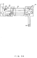
- Fig. 4 shows a configuration of a body-cavity-insertion diagnostic ultrasound system according to the present embodiment.
- the body-cavity-insertion diagnostic ultrasound system 1 has at least a signal controlling system 2 and an insertion tube (the insertion tube mainly consists of a bending section, a flexible tube 3, and an ultrasound probe 4).
- the diagnostic ultrasound system 2 has a control unit 2a.
- the control unit 2a controls the operations of a switch control signal generator 7 and performs signal processing on the ultrasonic reception signal transmitted from the ultrasound probe 4 via the bending section and the flexible tube 3 in order to convert the process signals into image signals.
- the insertion tube is shaped as a long tube, because it is inserted into body cavities.
- the ultrasound probe 4 has a cMUT 9 as an ultrasonic transducer. This cMUT 9 transmits and receives ultrasonic signals.
- the bending section is located at the back side of the ultrasound probe 4 and can be bent arbitrarily.
- the flexible tube is located at the back side of the bending section, and is long, narrow, and flexible.
- the insertion tube includes a bundle of coaxial cables used for the respective transducer elements that constitute the cMUT 9.
- the ultrasound probe 4 includes switches SW1 through SW4, an adder 5, a booster circuit 6, a switch control signal generator 7, a charge amplifier 8, and thecMUT9.
- the booster circuit 6 is a capacitive booster element that is formed on the semiconductor substrate by using the micromachining process. It is also possible to further form the adder 5, the switch control signal generator 7, the charge amplifier 8, and the cMUT 9 on the semiconductor substrate that is the same as this capacitive booster element by using the micromachining process or other semiconductor integration processes. Thereby, it is possible to make the ultrasound probe 4 smaller.
- a cMUT array (cMUT 9) has a configuration in which a plurality of ultrasonic transducer elements (or simply “elements”) that serve as the minimum unit for inputting and outputting drive control signals are arranged. Each of these elements consists of vibrators that are called transducer cells (or simply “cells”). The cell is a component that constitutes one cavity (blank space), as will be described.
- the switch control signal generator 7 generates control signals used for turning ON/OFF the switches SW1 through SW4. In other words, the switch control signal generator 7 generates signals that determine timings at which the respective switches are turned ON/OFF and determine periods during which the switches are in an ON/OFF state.
- Each of the switches SW1 through SW4 is made of a DMOS (Double Diffused MOSFET) or a VMOS (V-groove MOSFET).
- the adder 5 superposes the driving pulses for driving the cMUT 9 on the DC voltage boosted by the booster circuit 6.
- the driving pulses are generated by the switch SW2.
- the charge amplifier 8 has a function of performing impedance conversion (conversion from a high impedance to a low impedance), a function of detecting electric charges on the surface of the electrodes in the cMUT 9, and a function of amplification.
- the function of detecting the electric charges is a function of detecting the electric charges that changes on the upper electrode in response to the vibrations of the membrane corresponding to the intensity of the echo signals received in the cMUT 9.
- switch control signal generator 7 When transmitting ultrasound beams, switch control signal generator 7 turns on the switch SW3, and turns off the switch SW4.
- voltage V in and voltage V CC are input into the booster circuit 6.
- voltages V in and V CC are explained.
- the voltages transmitted in the coaxial cables are much smaller than the cMUT driving voltage.
- the booster circuit 6 generates a DC voltage V dc that is obtained by boosting the voltages V in and V CC , and outputs this DC voltage V dc to the switch SW1.
- the booster circuit 6 outputs three steps of the DC voltages V dc (V dc1 ⁇ V dc2 ⁇ V dc3 ) obtained on the basis of the different levels of boosting.
- the switch SW1 can perform switching of , for example, three channels in the present embodiment.
- the switch SW1 switches these channels on the basis of the control signals of the switch control signal generator 7, and outputs one of the DC voltages V dc (V dc1 , V dc2 , V dc3 ) output from the booster circuit 6.
- the switch control signal generator 7 generates pulses used for driving the cMUT 9 on the basis of the cable transmission signals transmitted from the control unit 2a of the diagnostic ultrasound system 2. Then, the switch control signal generator 7 outputs these pulses to the switch SW2.
- the switch SW2 performs the ON/OFF operations on the basis of the pulses, and superposes the driving pulses on the DC voltage V dc via the switch SW3 and the adder 5.
- the superposed driving signals are output to the cMUT 9.
- a high voltage is applied to a pair of electrodes consisting of the upper electrode and the bottom electrode, and thereby these electrodes attract each other, and when the applied voltage becomes zero, the electrodes return to their original positions.
- This vibration of the membrane generates ultrasound, and the ultrasound is emitted in the upward direction of the upper electrode.
- the switch control signal generator 7 turns off the switch SW3, and turns on the switch SW4.
- the ultrasound emitted from the cMUT 9 is reflected in body cavities. Then, the reflected wave is received by the cMUT 9.
- the cMUT 9 converts the received reflected wave into electric signals.
- the reception signals converted into the electric signals are transmitted to the diagnostic ultrasound system 2 via the charge amplifier 8.
- the diagnostic ultrasound system 2 forms diagnostic ultrasound images on the basis of the reception signals.
- the booster circuit 6 will be explained by referring to Figs. 5 and 6 .
- Fig. 5 shows the principle of the booster circuit 6 according to the present embodiment.
- the circuit shown in Fig. 5 includes a Schmidt Trigger inverter 11, capacitors C 1 and C out , diodes D 1 and D 2 , and terminals 12 through 20.
- the Schmidt Trigger inverter 11 includes a CMOSFET(Complementary Metal Oxide Semiconductor Field Effect Transistor) 21 (Q 1 ) and a CMOSFET 22 (Q 2 ).
- V in of 10V op is applied, at a frequency of e.g., 7.5MHz, to a common gate connection terminal 16 of Q 1 and Q 2 that perform the push-pull operations (V CC is also 10V).
- the diode D 2 receives the forward bias (the forward voltage drop of the diode D 2 is also V D , and V D is at most 0.7V).
- V CC V D
- V out nearly equals 2V in
- the circuit shown in Fig. 5 operates as a voltage-doubler booster circuit.
- a high dielectric capacitor is used as the capacitor C 1 .
- This high dielectric capacitor consists of a ferroelectric thin film.
- the ferroelectric substance is a substance that has electric polarization even when an electric field is not applied from the external environment, and in this substance this polarization (spontaneous polarization) can be inverted by an electric field applied from the external environment.
- a typical example of a ferroelectric substance is a crystal having a perovskite structure.
- the polarization represents the hysteresis curve.
- SrBi 2 (Nb 1-x Ta x ) 2 O 9 is a ferroelectric substance.
- This SrBi 2 (Nb 1-x Ta x ) 2 O 9 is a highly durable ferroelectric material, and has a bismuth layer structure.
- the ferroelectric substance may be formed of a solid solution thin film consisting of one or both of BaTiO 3 and SrTiO 3 .
- the high dielectric substance may be formed of a dielectric thin film that does not contain heavy metals, and the dielectric thin film can be formed of high dielectric materials such as ZnO, AIN, Ta 2 O 5 or the like. These dielectric materials are environmentally friendly because they do not contain heavy metals.
- Fig. 6 shows the concept of the configuration of the booster circuit 6 according to the present embodiment.
- the booster circuit 6 includes N (N is a positive integer) number of circuits 10 shown in Fig. 5 in a cascade connection.
- N number of circuits 10 are in a cascade connection
- the voltage V out output from the Nth circuit can be expressed by the equation below. Accordingly, by changing the number of circuits 10 to be in a cascade connection, the level of voltage boosting can be controlled.
- V out N + 1 ⁇ V CC - V D
- V out nearly equals (N+1)V CC
- the switch SW1 has three channels (SW1a, SW1b, and SW1c).
- V out 19 (V CC -V D ) (when V CC » V D , V out nearly equals 19V CC ) is satisfied.
- the input voltage V CC can be boosted to about (N+1) times the value that would be obtained without a booster circuit. Further, it is possible to generate a DC high voltage from a low voltage.
- the RF high-voltage driving signal is obtained by branching the DC high-voltage signal and by turning on and off the switch SW2 with respect to the branched signals at a high speed. Then, by performing the additional superposition on the RF high-voltage driving signal and the DC high voltage by using the adder 5, the superposition signal to be applied to the cMUT 9 is obtained. Additionally, the frequency of the ultrasound to be transmitted from the cMUT is determined by the ON/OFF frequency of SW2.
- the cMUT 9 to which the high-voltage superposition signal is applied emits ultrasound from its membrane surface that is provided on the upper electrode.
- the emitted ultrasound is reflected from the living-body tissue, and the reflection wave is received by the cMUT 9.
- the cMUT 9 converts the reflection ultrasonic wave into electric signals.
- the reception signals that have been converted into electric signals are sent to the diagnostic ultrasound system 2 via the charge amplifier 8.
- the diagnostic ultrasound system 2 forms diagnostic ultrasound images on the basis of the reception signals.
- the booster circuit 6 By using the booster circuit 6, only a low-voltage signal is transmitted through the cables, and thereby it is possible to efficiently generate high-voltage pulses on which the DC bias voltage for driving the ultrasonic transducer is superposed in the probe. Also, it is possible to avoid the effect of noise caused by the cables.
- Fig. 7 is a timing chart showing the operations of the switches (SW) and driving voltage signals for transmitting ultrasound. Fig. 7 will be explained while referring to Fig. 4 .
- Numeral 34 denotes the waveform of the echo reception signal, and the cycle thereof is approximately equal to the cycle of turning ON and OFF SW2.
- SW3 is in an OFF state
- SW4 is in an ON state
- the cMUT 9 receives the ultrasound reflected by the living-body tissue.
- the ultrasound received by the cMUT 9 is converted into electric signals, and is output to the diagnostic ultrasound system 2 via the SW4 and the charge amplifier 8.
- the above explanation is about one element of the cMUT; however, the scope of the present invention is not limited to this explanation.
- a number of control channels corresponding to the number of elements can be configured.
- by providing a phase difference for each control channel for controlling the timing of the driving of the SW arranged on each control channel it becomes possible for the transmission beam to form.
- Fig. 8 shows an example of a plan view of the cMUT 9 according to the present embodiment.
- a plurality of cMUT elements 41 are arranged in a parallel connection on a cMUT chip 40.
- a plurality of bottom electrodes 42 are formed on each of the cMUT elements 41. The portion expressed as the bottom electrodes 42 corresponds to the cMUT cells.
- ultrasound is emitted.
- the respective bottom electrodes 42 are connected to one another via a interconnections 43.
- a wire 44 for supplying DC is arranged, and is connected to the bottom electrodes 42 arranged on the end of the respective cMUT elements 41.
- MOSFET Metal Oxide Semiconductor Field Effect Transistor
- the drain region of the MOSFET switch 45a and the wire 44 are connected to each other via a wire 52.
- the source region of the MOSFET switch 45a and the drain region of the MOSFET switch 45b are connected to each other.
- the source region of the MOSFET switch 45b and the bottom electrode 42 are connected to each other via a wire 54.
- the drain region of the MOSFET switch 45c, the wire 44, and the bottom electrode 42 are connected to one another via a wire 55.
- the source region of the MOSFET switch 45c and a charge amplifier 51 are connected to each other via a wire 56.
- Electrode pads 50 (50a, 50b, and 50c) for inputting Gate signal are provided on the respective MOSFET switches 45 (45a, 45b, and 45c).
- the MOSFET switches 45a, 45b, and 45c respectively correspond to the switches SW2, SW3, and SW4 shown in Fig. 4 .
- the adder 5 that is shown in Fig. 4 is omitted.
- the region on the left side of Fig. 8 corresponds to the booster circuit 6 shown in Fig. 4 .
- the booster circuit 60 consists of a capacitor region 61 (corresponding to the capacitor C out shown in Fig. 5 ), an switching region 62 for switching output voltage (corresponding to the switch SW1 shown in Fig. 4 ), an upper electrode 63 on a high-capacitance capacitor (corresponding to the capacitor C 1 shown in Fig. 5 ), a high dielectric thin film 64 (corresponding to the capacitor C 1 shown in Fig. 5 ), an electrode pad 65 for inputting a signal (corresponding to the electrode pad to which V in shown in Fig. 5 is input), and a Schmidt Trigger inverter circuit + diode region 66 (corresponding to the Schmidt Trigger inverter 11 and the diodes D 1 and D 2 ) .
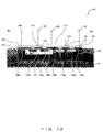
- Fig. 9 shows an example of a sectional view of the booster circuit region according to the present embodiment.
- Fig. 9 shows a view that corresponds to a sectional view of the booster circuit region 60 shown in Fig. 8 .
- the booster circuit region shown in Fig. 9 has the same functions as that in Fig. 8 , although the arrangement is partially changed from the arrangement in Fig. 8 for the purpose of explanation.
- the booster circuit region consists of a silicon substrate 71, a surface oxide film 72, bottom electrodes 73 and 74, high dielectric materials 75 and 76, upper electrodes 77 and 78, a CMOS converter circuit (CMOS FET + diode) 79, a ground wire 80, diffusion-regions-for-ohmic-contact 81 and 88, a MOSFET source region 82, a MOSFET drain region 83, a MOSFET channel region 84, a MOSFET gate wire 85, a diode-p-diffusion region 86, an n-diffusion region 87, and a diode region 89.
- CMOS FET + diode CMOS converter circuit
- Fig. 9 includes the silicon substrate 71 having thereon large capacitance thin film capacitors (or high dielectric constant materials 75 and 76, 75 and 76 respectively correspond to the capacitors C 1 and C out in Fig. 5 ) and the surface oxide film 72, the bottom electrodes 73 and 74, and the upper electrodes 77 and 78.
- the Schmidt Trigger inverter 79 (corresponding to the Schmidt Trigger inverter 11 in Fig. 5 ) that constitutes the voltage-doubler booster circuit and the diode region 89 (corresponding to the diodes D 1 and D 2 shown in Fig. 5 ) are formed on the silicon substrate 71.
- the channel region 84 corresponding to the CMOSFET 22 (Q 2 ) is connected in such a manner that the source side has the same potential via the diffusion-region 81 of the silicon substrate 71.
- the upper electrode 78 of one capacitor is connected to the silicon substrate 71 via the diffusion-region 88 in such a manner that the upper electrode 78 has the same potential.
- the ground wire 80 and the upper electrode 78 are also grounded.
- V in shown in Fig. 5 is input into the MOSFET gate wire 85.
- the upper electrode 78 is connected to the output unit of the Schmidt Trigger inverter of the next stage as shown in Fig. 6 , so that it will not cause the upper electrode 78 to have the same potential as that of the silicon substrate 71.
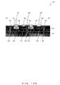
- Fig. 10 shows an example of a plan view of the booster circuit region according to the present embodiment.
- Fig. 10 is an enlarged view showing a region 67 enclosed by a dashed line in Fig. 8 .
- FECs ferroelectric thin film capacitors
- a p+ diffusion region 134 is formed on the FEC 102.
- a plurality of n diffusion regions 130 are formed on this p+ diffusion region 134.
- a CMOS inverter 110 and a pn junction diode 124 are formed on each of the n diffusion regions 130.
- the FEC 102, the CMOS inverter 110, and the pn junction diode 124 will be explained by referring to Figs. 11 through 13 .
- Fig. 11 shows a sectional view (on the plane Aa-Ab) of the FEC 102.
- This FEC 102 is formed by forming an insulation film (surface oxide film) 103 on the upper surface of the silicon substrate 101, and by forming a bottom electrode 105, a ferroelectric thin film 106, and an upper electrode 104 on the upper surface of the insulation film.
- a Pt or Au thin film with Ti and Cr formed as a buffer layer is used for the bottom electrode 105.
- Fig. 12 shows a sectional view (on the plane Ba-Bb) of the CMOS inverter 110.
- the configuration of the CMOS inverter 110 is as below.
- the p+ diffusion region 134 is formed, and the n diffusion region 130 is also formed.
- a p-well diffusion region 111 is formed, and on the p-well diffusion region 111, n+ diffusion regions 113 (113a and 113b) are formed.
- p+ diffusion regions 115 are formed on the n diffusion region 130.
- the CMOS inverter 110 consists of a p-channel MOSFET (p-MOS) (corresponding to Q 1 in Fig. 5 ) and an n-channel MOSFET (n-MOS) (corresponding to Q 2 in Fig. 5 ). Because an n-MOS is formed in an n-type substrate, an n-type substrate is formed on a p-type region (p well), and an n-MOS (Q 2 ) is formed. In this case, in order to avoid the parasitic MOSFET, n+ regions are provided below a lower side 148a of a source electrode 140 of the n-MOS and a lower side 148b of a bridge electrode serving as an output electrode. Similarly, in the p-MOS (Q 1 ), in order to avoid the parasitic MOSFET, n+ regions are provided below the lower side 148d of the source electrode 120 and the lower side 148c of a bridge electrode serving as an output electrode.
- p-MOS p-channel MOSFET
- insulation films 142 are formed on the upper surface of the n diffusion region 130; however, the upper surfaces of the n+ diffusion region 113 (113a and 113b) and the p+ diffusion regions 115 (115a and 115b) are not covered by the insulation films 142.
- an electrode 140 is formed on the upper surface of the n+ diffusion regions 113a that are not covered by the insulation films 142.
- the upper surface of the n+ diffusion region 113b that is not covered and the upper surface of the p+ diffusion region 115a are electrically continuous with each other via a bridge electrode 114.
- an electrode 143 is formed on the top surface of the p+ diffusion region 115b that is not covered. Also, gate electrodes 112 and 116 are formed on the insulation films 142.
- An electrode terminal 144 which supplies DC voltage to the CMOS inverter is provided to the electrode 140.
- An input terminal 145 of the CMOS inverter is provided to the gate electrodes 112 and 116.
- An output terminal 146 of the CMOS inverter is provided to the bridge electrodes 114.
- a ground terminal 147 of the CMOS inverter is provided to the electrode 143.
- the output terminal 146 corresponds to terminal 16 shown in Fig. 5 .
- the electrode terminal 144 corresponds to terminal 12 shown in Fig. 5 .
- the ground terminal 147 corresponds to terminal 13 shown in Fig. 5 .
- Fig. 13A shows a sectional view (on the plane Ca-Cb) of the pn junction diode 124.
- Fig. 13B shows the configuration of Fig. 13A in a simplified manner.
- the configuration of the pn junction diode 124 is as below.
- the p+ diffusion region 134 is formed, and the n diffusion region 130 is further formed.
- p diffusion regions 120 and 122 and n+ diffusion regions 121 and 123 are formed.
- p+ isolation regions 154 and 156 are formed on a part of the n diffusion region 130 and of the p+ diffusion region 134.
- the upper surfaces of the p diffusion regions 120 and 122 and of the n+ diffusion regions 121 and 123 are not covered by insulation films 150.
- an electrode 151 is formed on the upper surface of the p diffusion region 120 that is not covered.
- the upper surface of the n+ diffusion region 121 that is not covered and the upper surface of the p+ diffusion region 122 are electrically continuous to each other via a bridge electrode 152.
- an electrode 153 is formed on the top surface of the n+ diffusion region 123 that is not covered.
- An input terminal 157 is provided to the electrode 151.
- a common terminal 158 is provided to the bridge electrode 152.
- An output terminal 159 is provided to the electrode 153.
- the input terminal 157 corresponds to the terminal 17 shown in Fig. 5 .
- the common terminal 158 corresponds to the terminal 19 shown in Fig. 5 .
- the output terminal 159 corresponds to the terminal 18 shown in Fig. 5 .
- Fig. 10 is again referred to.
- the upper electrode 104 of the FEC 102 and the bridge electrode 152 of the pn junction diode 124 are electrically continuous to each other via an upper electrode wire 125 of the FEC 102.
- the n+ diffusion region 123 of the pn junction diode 124 is electrically continuous with the p diffusion region 120 of the pn junction diode 124 of the next stage via a connection wire 132.
- the bridge electrode 114 and the gate electrodes 112 and 116 of the CMOS inverter 110 are electrically continuous with the bottom electrode 105 via wires 118 and 133.
- the electrode terminal 144 and a wire 135 which supplies DC voltage to the electrode terminal 144 are connected to each other.
- a ground terminal 147 of the CMOS inverter 110 and a ground wire 131 are connected to each other.
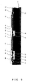
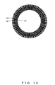
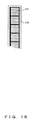
- Figs. 14 through 17 in which a group of cMUT units consisting of a plurality of cMUT elements being integrated are arranged in a cylindrical shape.
- the configuration shown in Figs. 14 through 17 is only one example of the arrangement, and is not intended to limit the scope of the present invention.
- Fig. 14 is a top view of the group of cMUT units arranged in a cylindrical shape.
- Fig. 15 is a side view of the group of cMUT units arranged in a cylindrical shape.
- Each cMUT unit 161 consists of a plurality (for example, forty-eight) of the cMUT elements.
- Each element consists of a plurality of the cMUT cells.
- the cMUT units 161 are provided on through-hole flexible printed circuit boards (through-hole FPCs) 162. On the bottom surfaces of the through-hole FPCs 162, control circuit units 163 respectively corresponding to the cMUT units 161 are provided. On the through-hole FPCs 162, through holes are made so that the electrodes of the respective elements are connected to the terminal pads for inputting/outputting signals of the control circuit units 163.
- cMUT array units that are in a planar configuration are produced by using the MEMS technique.
- the cMUT array units and the control circuit unit integration circuits are jointed.
- the dicing is performed on the cMUT array units and the control circuit unit integration circuits in order to divide them into units. Thereafter, the structure that has undergone the dicing process is rounded into a cylindrical shape.
- Fig. 16 is an enlarged view showing the cMUT unit 161.
- the cMUT unit 161 consists of a plurality of cMUT elements 171 provided on a flexible printed circuit board (FPC) 172.
- FPC flexible printed circuit board
- Fig. 17 is an enlarged view showing the cMUT element 171.
- the cMUT element 171 consists of a plurality of transducer cells 180.
- An electrode 181 is provided to each of the transducer cells 180.
- the electrodes 181 are connected to the booster circuit.
- a DC high-voltage unit including an input terminal for inputting an alternating-current low voltage, a CMOS inverter circuit, a thin film capacitor, a diode, an output terminal for outputting a DC high-voltage signal, and the like can be formed on one and the same semiconductor substrate.
- a DC high-voltage unit including an input terminal for inputting an alternating-current low voltage, a CMOS inverter circuit, a thin film capacitor, a diode, an output terminal for outputting a DC high-voltage signal, and the like can be formed on one and the same semiconductor substrate.
- an adder, a charge amplifier, a semiconductor switch, a semiconductor switch control unit, and the like on this semiconductor body, and accordingly it is possible to further reduce the size.
- a high-voltage generation unit is formed in a cMUT mounted in a body-cavity-insertion diagnostic ultrasound system.
- the scope of the present invention is not limited to this explanation, and it is possible to incorporate the unit into a device such as an ultrasound catheter, an ultrasound capsule endoscope or the like.
Landscapes
- Health & Medical Sciences (AREA)
- Life Sciences & Earth Sciences (AREA)
- Engineering & Computer Science (AREA)
- General Health & Medical Sciences (AREA)
- Physics & Mathematics (AREA)
- Pathology (AREA)
- Surgery (AREA)
- Public Health (AREA)
- Biomedical Technology (AREA)
- Heart & Thoracic Surgery (AREA)
- Medical Informatics (AREA)
- Molecular Biology (AREA)
- Nuclear Medicine, Radiotherapy & Molecular Imaging (AREA)
- Animal Behavior & Ethology (AREA)
- Biophysics (AREA)
- Radiology & Medical Imaging (AREA)
- Veterinary Medicine (AREA)
- Mechanical Engineering (AREA)
- Chemical & Material Sciences (AREA)
- Analytical Chemistry (AREA)
- Biochemistry (AREA)
- General Physics & Mathematics (AREA)
- Immunology (AREA)
- Ultra Sonic Daignosis Equipment (AREA)
- Transducers For Ultrasonic Waves (AREA)
Abstract
Description
- The present invention relates to ultrasonic transducer devices that are included in ultrasound scopes, in ultrasound miniature probes, and in ultrasound capsule endoscopes, and that are manufactured by using the micromachining processes, and also relates to a method of controlling the same.
- The diagnostic ultrasound method, in which ultrasound is emitted onto walls of body cavities and the state of the body is visualized on the basis of the signals echoed from the walls for making a diagnosis, is widely used. One of the instruments used for the diagnostic ultrasound method is an ultrasound endoscope scope.
- An ultrasound endoscope scope has an ultrasound probe at the distal end of the insertion tube that is to be inserted into body cavities . The ultrasound probe converts electric signals into ultrasound to emit onto body cavities, and receives the ultrasound reflected in the body cavities in order to convert the received ultrasound into electric signals.
- Conventionally, for manufacturing ultrasound probes, piezoelectric ceramics (PZT: lead-zirconate-titanate) have been used as the piezoelectric device used for converting electric signals into ultrasound.
- In recent years, capacitive micromachined ultrasonic transducers (hereinafter referred to as cMUTs) obtained by processing a silicon semiconductor substrate have gathered interest. A cMUT is one of several MEMS (Micro Electro-Mechanical System) devices.
- A diagnosis modality called harmonic imaging has attracted lots of attention because it permits an ultrasonic diagnosis with a high level of accuracy that the conventional methods have never been able to attain. Accordingly, it has become essential for the body-cavity-insertion-diagnostic ultrasound systems to be compatible with this diagnosis modality. Because of this, it has been desirable to have ultrasonic transducers with broader bandwidths.
- As is mentioned above, cMUTs that are manufactured using micromachining processes have recently gathered interest. The merit of cMUTs is not only that they do not contain heavy metals such as lead or the like, but also that wide bandwidth characteristics can be achieved easily. Accordingly, cMUTs are suitable for harmonic imaging.
-
Fig. 1 shows an example of a conventional cMUT. The cMUT shown inFig. 1 is the cMUT disclosed inPatent Document 1. This ultrasonic transducer is constituted of a plurality of cMUTs. Respective cells that constitute each cMUT have acharged membrane 206. Thischarged membrane 206 has capacitance and is opposed to asubstrate 205 that is inversely charged. - This
charged membrane 206 is curved by the bias charging in the direction of thesubstrate 205. Also, thesubstrate 205 has a center that is elevated in such a manner that the elevated portion gets closer to the center of thecharged membrane 206 so that the density of the charged particles is the highest around the center of the vibration of thecharged membrane 206. For the purpose of realizing the operations by using harmonics, the driving pulse waveform provided to the cells are distorted in advance. This is because the non-linear operations of devices are considered in order to reduce the harmonic components that may be generated in transmission ultrasound by a driving signal that does not have distortion. - cMUT cells can be integrated with a transducer controlling circuit such as a
bias charging regulator 201 because the cMUT cells are processed by using conventional semiconductor processing methods. The cMUT cells can be processed also by using micro-stereolithography. Accordingly, the cells are formed by using various materials such as polymers and the like. - The above mentioned diagnostic ultrasound system has a high voltage-proof switch in the ultrasound probes so that it can operate at a high voltage. The diagnostic ultrasound system has a pulse generation unit and a control unit. The pulse generation unit can output pulses that have arbitrary waveforms and arbitrary voltage values. The control unit controls the outputs from the above high voltage-proof switch and pulse generation unit on the basis of the scanning timing of the ultrasonic transducer.
- In this situation, the present applicants have suggested a method in which the DC voltage is applied only at a timing that corresponds to the application of the rf signal (Patent Document 2).
-
Fig. 2 shows a first example of a method of driving an ultrasonic transducer; this method has been employed in the conventional piezoelectric transducer driving techniques. The example shown inFig. 2 is of a probe that is disclosed inPatent Document 3. This probe includes, in addition to the known circuits, an additional operation circuit in order to minimize the influence of electrical interference that can be caused by a cable that is used for connecting the probe and the ultrasound signal evaluation device and that is relatively long. In the technique disclosed inPatent Document 3, the probe includes the above described circuit; however, the circuit is not so large. Also, the operations for the ultrasound inspection are not so difficult. - The probe housing of the probe includes a
transmission circuit 210. Thetransmission circuit 210 includes abooster coil 211, a VMOS field effect transistor (VMOS FET) 213, acontrol circuit 214, and acapacitor 215. The VMOS FET 213 is turned on and off in accordance with acontrol signal 212. - The operations of the
transmission circuit 210 are explained hereinbelow. First, thecapacitor 215 is charged at a high density via thebooster coil 211. When the amount of the charge in thecapacitor 215 reaches the upper limit, a control signal is output from thecontrol circuit 214 to the switch driving terminal in the VMOS FET 213. Then, the VMOS FET 213 enters an ON state. Then, the discharging starts in the closed circuit of the ON state resistance, aresistor 216, and thecapacitor 215. The voltage generated by this discharged current in theresistor 216 is applied to a piezoelectric transducer. - However, when a high voltage is to be induced using this method, the
booster coil 211 has to have a high inductance. If thebooster coil 211 has a high inductance, a resonance is caused by thecapacitor 215 and thebooster coil 211, and the driving pulse comes to include ringing. This ringing signal is applied to the piezoelectric transducer without being reduced or blocked, which causes deterioration in the spatial resolution and the S/N ratio. -
Figs. 3A and3B show a second example of a method of driving a piezoelectric ultrasonic transducer that has been employed in the conventional techniques.Fig. 3A shows a diagnostic ultrasound system disclosed inPatent Document 4.Fig. 3B shows the same system in a simplified manner.Patent Document 4 discloses a configuration for minimizing the influence of the electric interference caused by a long connection cable, although the technique disclosed in this document is not intended to have a countermeasure against the above ringing. - In
Figs. 3A and3B , anultrasound probe 220 and adiagnostic ultrasound system 221 are shown. Ultrasound signals are emitted and received by anultrasonic transducer 222 provided in the ultrasound probe in order to perform the ultrasound scan on the subject. Thediagnostic ultrasound system 221 can obtain an ultrasound sectional image on the basis of the received ultrasound signals. - In the
ultrasound probe 220, a high voltage-proof switch 223 is provided. In the abovediagnostic ultrasound system 221, apulse generation unit 227 and acontrol unit 228 are provided. Thepulse generation unit 227 can output a pulse that has an arbitrary voltage value in an arbitrary waveform. Thecontrol unit 228 controls the output of the voltage-proof switches 223 and thepulse generation unit 227 in accordance with the timing of the scan performed by the ultrasonic transducer. - By the above configuration, the size of the electric circuit in the ultrasound probe is reduced. Also, high voltage pulse signals for driving the ultrasonic transducer can be generated efficiently in the probe. Also, excellent ultrasound images that are not influenced by the interference caused by the cable can be obtained, and noise that leaks to the external environment can be reduced. Also, the ringing is not causedbecause there is no element that can cause resonation in the circuit.
- As described above, it has been proposed to produce a micro piezoelectric transformer and a micro electromagnetic transformer and to arrange them close to a cMUT and a pMUT (a piezoelectric transducer that is produced by using the micromachining processes).
- Patent Document 1:
Japanese Patent Application Publication (translation of PCT application) No.2004-503313 - Patent Document 2:
Japanese Patent Application Publication No.2004-176039 - Patent Document 3:
Japanese Examined Patent Application No.63-026341 - Patent Document 4:
Japanese Patent Application No.3062313 - A cMUT device according to the present invention comprises:
- a cMUT formed on a semiconductor substrate;
- a DC high-voltage generation unit that is provided on the semiconductor substrate and that is for generating a DC high-voltage signal to be superposed on a driving signal for the cMUT;
- a driving signal generation unit that is provided on the semiconductor substrate and that is for generating the driving signal; and
- a superposition unit that is provided on the semiconductor substrate and that is for branching the DC high-voltage signal output from the DC high-voltage generation unit and for superposing one of the branched DC high-voltage signals on the other of the branched DC high-voltage signals via the driving signal generation unit.
- A method of controlling a cMUT device according to the present invention comprises:
- a cMUT formed on a semiconductor substrate;
- a DC high-voltage generation unit that is provided on the semiconductor substrate and that is for generating a DC high-voltage signal to be superposed on a driving signal for the cMUT;
- a first switching unit switching output levels of the DC high-voltage signal output from the DC high-voltage generation unit;
- driving signal generation unit that is provided on the semiconductor substrate and that is for generating the driving signal;
- a superposition unit that is provided on the semiconductor substrate and that is for superposing the driving signal on the DC high-voltage signal;
- a second switching unit that is provided on the semiconductor substrate and that controls the driving signal or the DC high-voltage signal, which is input into the superposition unit; and
- a third switching unit that is provided on the semiconductor substrate and that controls an ultrasonic reception signal being converted into an electric signal by the cMUT and controls the converted electric signal, which is output to an external environment, in which:
- if ultrasound is to be transmitted from the cMUT device, the first switching unit is driven, and the output level of the DC high-voltage signal is set;
- the driving signal generation unit is driven and the driving signal is generated;
- the second switching unit is driven so that the driving signal and the DC high voltage signal are input into the superposition unit; and
- the third switching unit is caused to be in an OFF state.
-
-
Fig. 1 shows an example of a conventional cMUT; -
Fig. 2 shows a first example of a method of driving an ultrasonic transducer that been employed in the conventional techniques; -
Fig. 3A shows a second example of a method of driving an ultrasonic transducer that has been employed in the conventional techniques; -
Fig. 3B shows in a simplified manner the system shown inFig. 3A ; -
Fig. 4 shows a configuration of a transmitting and receiving circuit system for body-cavity-insertion diagnostic ultrasound system according to the present embodiment; -
Fig. 5 shows the principle of abooster circuit 6 according to the present embodiment; -
Fig. 6 shows the configuration of thebooster circuit 6 according to the present embodiment; -
Fig. 7 is a timing chart showing the operations of switches (SW), driving and received voltage signals for transmitting and received ultrasound; -
Fig. 8 shows an example of a plan view of the cMUT 9 according to the present embodiment; -
Fig. 9 shows an example of a sectional view of a booster circuit region according to the present embodiment; -
Fig. 10 shows an example of a plan view of the booster circuit region according to the present embodiment; -
Fig. 11 shows an example of a sectional view (on the plane Aa-Ab) of a ferroelectric thin film capacitor (FEC) 102; -
Fig. 12 shows a sectional view (on the plane Ba-Bb) of aCMOS inverter 110; -
Fig. 13A shows a sectional view (on the plane Ca-Cb) of a pn-junction diode 124; -
Fig. 13B shows the configuration ofFig. 13A in a simplified manner; -
Fig. 14 is a top view of a group of cMUT units arranged in a cylindrical shape; -
Fig. 15 is a side view of the group of the cMUT units arranged in a cylindrical shape; -
Fig. 16 is an enlarged view showing acMUT unit 161; and -
Fig. 17 is an enlarged view showing acMUT element 171. - Conventionally, miniature piezoelectric transformers and miniature electromagnetic transformers have been produced in a discrete manner and have been arranged close to cMUTs and pMUTs. However, in this method, the size of electric circuits can only be reduced to some extent, and a high level of quality management has been required because of complicated wiring and connection.
- Meanwhile, to form a high-voltage generation unit on or in a silicon substrate that is the same as an ultrasonic transducer produced by using the micromachining process has not been suggested conventionally.
- Accordingly, by using the micromachining process or the semiconductor integration process, the present invention forms a DC high-voltage generation unit on or in a silicon substrate that is the same as an ultrasonic transducer produced by using the micromachining process. Thereby, the reduction of the size of the cMUT devices is realized.
- In other words, in a cMUT according to the present invention, DC high-voltage generation unit and devices such as a semiconductor switch, a charge amplifier, or the like are arranged in an integrated manner close to the capacitive ultrasonic transducer on a semiconductor substrate. Thereby, the reduction of the size of the cMUT devices is realized.
-
Fig. 4 shows a configuration of a body-cavity-insertion diagnostic ultrasound system according to the present embodiment. The body-cavity-insertiondiagnostic ultrasound system 1 has at least asignal controlling system 2 and an insertion tube (the insertion tube mainly consists of a bending section, aflexible tube 3, and an ultrasound probe 4). - The
diagnostic ultrasound system 2 has acontrol unit 2a. Thecontrol unit 2a controls the operations of a switchcontrol signal generator 7 and performs signal processing on the ultrasonic reception signal transmitted from theultrasound probe 4 via the bending section and theflexible tube 3 in order to convert the process signals into image signals. - The insertion tube is shaped as a long tube, because it is inserted into body cavities. The
ultrasound probe 4 has a cMUT 9 as an ultrasonic transducer. This cMUT 9 transmits and receives ultrasonic signals. The bending section is located at the back side of theultrasound probe 4 and can be bent arbitrarily. The flexible tube is located at the back side of the bending section, and is long, narrow, and flexible. The insertion tube includes a bundle of coaxial cables used for the respective transducer elements that constitute the cMUT 9. - The
ultrasound probe 4 includes switches SW1 through SW4, anadder 5, abooster circuit 6, a switchcontrol signal generator 7, acharge amplifier 8, and thecMUT9. Thebooster circuit 6 is a capacitive booster element that is formed on the semiconductor substrate by using the micromachining process. It is also possible to further form theadder 5, the switchcontrol signal generator 7, thecharge amplifier 8, and the cMUT 9 on the semiconductor substrate that is the same as this capacitive booster element by using the micromachining process or other semiconductor integration processes. Thereby, it is possible to make theultrasound probe 4 smaller. - A cMUT array (cMUT 9) has a configuration in which a plurality of ultrasonic transducer elements (or simply "elements") that serve as the minimum unit for inputting and outputting drive control signals are arranged. Each of these elements consists of vibrators that are called transducer cells (or simply "cells"). The cell is a component that constitutes one cavity (blank space), as will be described.
- The switch
control signal generator 7 generates control signals used for turning ON/OFF the switches SW1 through SW4. In other words, the switchcontrol signal generator 7 generates signals that determine timings at which the respective switches are turned ON/OFF and determine periods during which the switches are in an ON/OFF state. Each of the switches SW1 through SW4 is made of a DMOS (Double Diffused MOSFET) or a VMOS (V-groove MOSFET). - The
adder 5 superposes the driving pulses for driving the cMUT 9 on the DC voltage boosted by thebooster circuit 6. The driving pulses are generated by the switch SW2. - The
charge amplifier 8 has a function of performing impedance conversion (conversion from a high impedance to a low impedance), a function of detecting electric charges on the surface of the electrodes in the cMUT 9, and a function of amplification. The function of detecting the electric charges is a function of detecting the electric charges that changes on the upper electrode in response to the vibrations of the membrane corresponding to the intensity of the echo signals received in the cMUT 9. - Next, the operations of the body-cavity-insertion
diagnostic ultrasound system 1 will be explained. First, the transmission of ultrasound beams is explained. - When transmitting ultrasound beams, switch
control signal generator 7 turns on the switch SW3, and turns off the switch SW4. - Next, voltage Vin and voltage VCC are input into the
booster circuit 6. Here, voltages Vin and VCC are explained. There is a method of generating VCC by transmitting the alternating-current voltage Vin in the coaxial cable in the insertion tube and providing a rectifier circuit in thebooster circuit 6, and a method of generating Vin by transmitting the DC voltage VCC in the coaxial cables and providing an oscillator circuit in the booster circuit. In both methods, the voltages transmitted in the coaxial cables are much smaller than the cMUT driving voltage. - The
booster circuit 6 generates a DC voltage Vdc that is obtained by boosting the voltages Vin and VCC, and outputs this DC voltage Vdc to the switch SW1. In the present embodiment, thebooster circuit 6 outputs three steps of the DC voltages Vdc (Vdc1 < Vdc2 < Vdc3) obtained on the basis of the different levels of boosting. - The switch SW1 can perform switching of , for example, three channels in the present embodiment. The switch SW1 switches these channels on the basis of the control signals of the switch
control signal generator 7, and outputs one of the DC voltages Vdc (Vdc1, Vdc2, Vdc3) output from thebooster circuit 6. - Also, the switch
control signal generator 7 generates pulses used for driving the cMUT 9 on the basis of the cable transmission signals transmitted from thecontrol unit 2a of thediagnostic ultrasound system 2. Then, the switchcontrol signal generator 7 outputs these pulses to the switch SW2. The switch SW2 performs the ON/OFF operations on the basis of the pulses, and superposes the driving pulses on the DC voltage Vdcvia the switch SW3 and theadder 5. - The superposed driving signals are output to the cMUT 9. In the cMUT 9, a high voltage is applied to a pair of electrodes consisting of the upper electrode and the bottom electrode, and thereby these electrodes attract each other, and when the applied voltage becomes zero, the electrodes return to their original positions. This vibration of the membrane generates ultrasound, and the ultrasound is emitted in the upward direction of the upper electrode.
- Next, reception of ultrasound beams will be explained. When receiving the ultrasound beams, the switch
control signal generator 7 turns off the switch SW3, and turns on the switch SW4. - The ultrasound emitted from the cMUT 9 is reflected in body cavities. Then, the reflected wave is received by the cMUT 9. The cMUT 9 converts the received reflected wave into electric signals. The reception signals converted into the electric signals are transmitted to the
diagnostic ultrasound system 2 via thecharge amplifier 8. Thediagnostic ultrasound system 2 forms diagnostic ultrasound images on the basis of the reception signals. - Next, the
booster circuit 6 will be explained by referring toFigs. 5 and6 . -
Fig. 5 shows the principle of thebooster circuit 6 according to the present embodiment. The circuit shown inFig. 5 includes aSchmidt Trigger inverter 11, capacitors C1 and Cout, diodes D1 and D2, andterminals 12 through 20. TheSchmidt Trigger inverter 11 includes a CMOSFET(Complementary Metal Oxide Semiconductor Field Effect Transistor) 21 (Q1) and a CMOSFET 22 (Q2). - Next, the operation principle of the circuit shown in
Fig. 5 will be explained. A rectangular wave Vin of 10Vop is applied, at a frequency of e.g., 7.5MHz, to a commongate connection terminal 16 of Q1 and Q2 that perform the push-pull operations (VCC is also 10V). - When 10V is applied to the common
gate connection terminal 16, Q1 is ON and Q2 is OFF. Then, the diode D1 receives the forward bias, and the voltages Vcl = VCC-VD (VD is the forward voltage drop of the diode D1, and VD is at most 0.7V) is applied to the capacitor C1. - Meanwhile, the capacitor Cout is charged, and the voltage of Vout = VCC - 2VD is accumulated in the capacitor Cout. Also, the diode D2 receives the forward bias (the forward voltage drop of the diode D2 is also VD, and VD is at most 0.7V).
- Next, when Vin = 0, Q1 becomes OFF, and Q2 becomes ON, and the diode D1 receives the reverse bias; accordingly, a voltage is supplied to the negative terminal of the capacitor C1. Then, Cout is charged via the diode D2 receiving the forward bias. In other words, as a result of the positive terminal of the capacitor C1 being boosted, a voltage higher than the supplied voltage VCC can be obtained.
- When the capacitance of the capacitor Cout is smaller than the capacitance of the capacitor C1, the equation Vout = Vout1 + Vc1 = 2 (Vin-VD) is satisfied (where Vout1 is the forward voltage drop of Q1) . When VCC >> VD, Vout nearly equals 2Vin, and the circuit shown in
Fig. 5 operates as a voltage-doubler booster circuit. - As described above, it is desirable to make the capacitance of the capacitor C1 larger than the capacitance of the capacitor Cout. Accordingly, a high dielectric capacitor is used as the capacitor C1. This high dielectric capacitor consists of a ferroelectric thin film. The ferroelectric substance is a substance that has electric polarization even when an electric field is not applied from the external environment, and in this substance this polarization (spontaneous polarization) can be inverted by an electric field applied from the external environment.
- A typical example of a ferroelectric substance is a crystal having a perovskite structure. When the alternating voltage is applied to ferroelectric substances, the polarization represents the hysteresis curve. SrBi2(Nb1-xTax)2O9 is a ferroelectric substance. This SrBi2(Nb1-xTax)2O9 is a highly durable ferroelectric material, and has a bismuth layer structure.
- Also, the ferroelectric substance may be formed of a solid solution thin film consisting of one or both of BaTiO3 and SrTiO3. Also, the high dielectric substance may be formed of a dielectric thin film that does not contain heavy metals, and the dielectric thin film can be formed of high dielectric materials such as ZnO, AIN, Ta2O5 or the like. These dielectric materials are environmentally friendly because they do not contain heavy metals.
-
Fig. 6 shows the concept of the configuration of thebooster circuit 6 according to the present embodiment. Thebooster circuit 6 includes N (N is a positive integer) number ofcircuits 10 shown inFig. 5 in a cascade connection. When N number ofcircuits 10 are in a cascade connection, the voltage Vout output from the Nth circuit can be expressed by the equation below. Accordingly, by changing the number ofcircuits 10 to be in a cascade connection, the level of voltage boosting can be controlled.
When VCC >> VD,
Vout nearly equals (N+1)VCC - In
Fig. 6 , the switch SW1 has three channels (SW1a, SW1b, and SW1c). When SW1a = ON, SW1b = OFF, and SW1c = OFF, the sixcircuits 10 are in a cascade connection, and accordingly the equation Vout = 7(VCC-VD) (when VCC >> VD, Vout nearly equals 7VCC) is satisfied. When SWla = OFF, SW1b = ON, and SW1c = OFF, twelvecircuits 10 are in a cascade connection, and accordingly the equation Vout = 13 (VCC-VD) (when VCC >> VD, Vout nearly equals 13VCC) is satisfied. When SW1a = OFF, SW1b = OFF, and SW1c = ON, eighteencircuits 10 are in a cascade connection, and accordingly the equation Vout = 19 (VCC-VD) (when VCC » VD, Vout nearly equals 19VCC) is satisfied. - As described above, by using a booster circuit, the input voltage VCC can be boosted to about (N+1) times the value that would be obtained without a booster circuit. Further, it is possible to generate a DC high voltage from a low voltage.
- When transmitting ultrasound beams, the switch SW3 = ON, and the switch SW4 = OFF. Then, by using the switch SW2, the RF high-voltage driving signal is superposed on the boosted DC high voltage, and the superposition signal is applied to the bottom electrode in the cMUT. The RF high-voltage driving signal is obtained by branching the DC high-voltage signal and by turning on and off the switch SW2 with respect to the branched signals at a high speed. Then, by performing the additional superposition on the RF high-voltage driving signal and the DC high voltage by using the
adder 5, the superposition signal to be applied to the cMUT 9 is obtained. Additionally, the frequency of the ultrasound to be transmitted from the cMUT is determined by the ON/OFF frequency of SW2. - The cMUT 9 to which the high-voltage superposition signal is applied emits ultrasound from its membrane surface that is provided on the upper electrode. The emitted ultrasound is reflected from the living-body tissue, and the reflection wave is received by the cMUT 9.
- When receiving ultrasound beams, switch SW3 = OFF and switch SW4 = ON. The cMUT 9 converts the reflection ultrasonic wave into electric signals. The reception signals that have been converted into electric signals are sent to the
diagnostic ultrasound system 2 via thecharge amplifier 8. Thediagnostic ultrasound system 2 forms diagnostic ultrasound images on the basis of the reception signals. - By using the
booster circuit 6, only a low-voltage signal is transmitted through the cables, and thereby it is possible to efficiently generate high-voltage pulses on which the DC bias voltage for driving the ultrasonic transducer is superposed in the probe. Also, it is possible to avoid the effect of noise caused by the cables. -
Fig. 7 is a timing chart showing the operations of the switches (SW) and driving voltage signals for transmitting ultrasound.Fig. 7 will be explained while referring toFig. 4 .Fig. 7 shows anultrasound transmission period 30 and an echosignal reception period 31. A period that consists of theultrasound transmission period 30 and the echosignal reception period 31 is repeated. T (= 1 through 4) represents the transmission period. - When the timing T = 1, SW3 becomes ON. Then, SW4 is in an OFF state. Then, SW1 becomes ON (strictly, one of SW1a, SW1b, and SW1c becomes ON) . Then, the Vin and VCC are input into the
booster circuit 6, and the DC voltage Vdc that is at a high-voltage level is output from thebooster circuit 6. - When the timing T = 2, SW2 becomes ON. Then, the ON voltage Vdc of SW2 is further additionally superposed on the DC voltage Vdc, and is applied to the cMUT 9.
- When the timing T = 3, SW2 becomes OFF. Then, the ON voltage Vdc of SW2 is blocked, and accordingly the voltage applied to the cMUT 9 is Vdc.
- T = 4 and T = 5 are respectively repeats of the operations of T = 1 and T = 2.
- As described above, variations are caused between 2Vdc and Vdc at a high speed. In other words, a high voltage superposition driving signal voltage Vdrvwhose amplitude is Vdc and whose DC bias voltage is 1.5Vdc is generated, and this is applied to the cMUT 9, and the cMUT 9 emits ultrasound.
- T = 5 through T = 16 are the echo signal reception periods.
Numeral 34 denotes the waveform of the echo reception signal, and the cycle thereof is approximately equal to the cycle of turning ON and OFF SW2. During the echo signal reception periods, SW3 is in an OFF state, SW4 is in an ON state, and the cMUT 9 receives the ultrasound reflected by the living-body tissue. The ultrasound received by the cMUT 9 is converted into electric signals, and is output to thediagnostic ultrasound system 2 via the SW4 and thecharge amplifier 8. - Additionally, the above explanation is about one element of the cMUT; however, the scope of the present invention is not limited to this explanation. For example, even in the case of one-dimensionally or two-dimensionally array, a number of control channels corresponding to the number of elements can be configured. Also, by providing a phase difference for each control channel for controlling the timing of the driving of the SW arranged on each control channel, it becomes possible for the transmission beam to form. Further, by performing the reception beam forming process on the output from the plurality of the
charge amplifiers 8, a linear scan or a sector scan can be performed accurately. - Next, the configuration in which the cMUT according to the present embodiment and the driving control circuit formed in a monolithic manner are integrated will be explained.
-
Fig. 8 shows an example of a plan view of the cMUT 9 according to the present embodiment. InFig. 8 , a plurality ofcMUT elements 41 are arranged in a parallel connection on acMUT chip 40. A plurality ofbottom electrodes 42 are formed on each of thecMUT elements 41. The portion expressed as thebottom electrodes 42 corresponds to the cMUT cells. When the membranes of the respective cMUT cells vibrate, ultrasound is emitted. - The respective
bottom electrodes 42 are connected to one another via ainterconnections 43. On the upper portion of thecMUT chip 40, awire 44 for supplying DC is arranged, and is connected to thebottom electrodes 42 arranged on the end of the respectivecMUT elements 41. - In
Fig. 8 , on a region between thewire 44 and thecMUT elements 41, MOSFET (Metal Oxide Semiconductor Field Effect Transistor) switches 45 (45a, 45b, and 45c) and acharge amplifier 51 are provided. - The drain region of the
MOSFET switch 45a and thewire 44 are connected to each other via awire 52. The source region of theMOSFET switch 45a and the drain region of theMOSFET switch 45b are connected to each other. The source region of theMOSFET switch 45b and thebottom electrode 42 are connected to each other via awire 54. The drain region of theMOSFET switch 45c, thewire 44, and thebottom electrode 42 are connected to one another via awire 55. The source region of theMOSFET switch 45c and acharge amplifier 51 are connected to each other via awire 56. Electrode pads 50 (50a, 50b, and 50c) for inputting Gate signal are provided on the respective MOSFET switches 45 (45a, 45b, and 45c). - The MOSFET switches 45a, 45b, and 45c respectively correspond to the switches SW2, SW3, and SW4 shown in
Fig. 4 . InFig. 8 , theadder 5 that is shown inFig. 4 is omitted. - The region on the left side of
Fig. 8 (a booster circuit region 60) corresponds to thebooster circuit 6 shown inFig. 4 . Thebooster circuit 60 consists of a capacitor region 61 (corresponding to the capacitor Cout shown inFig. 5 ), an switchingregion 62 for switching output voltage (corresponding to the switch SW1 shown inFig. 4 ), anupper electrode 63 on a high-capacitance capacitor (corresponding to the capacitor C1 shown inFig. 5 ), a high dielectric thin film 64 (corresponding to the capacitor C1 shown inFig. 5 ), anelectrode pad 65 for inputting a signal (corresponding to the electrode pad to which Vin shown inFig. 5 is input), and a Schmidt Trigger inverter circuit + diode region 66 (corresponding to theSchmidt Trigger inverter 11 and the diodes D1 and D2) . -
Fig. 9 shows an example of a sectional view of the booster circuit region according to the present embodiment.Fig. 9 shows a view that corresponds to a sectional view of thebooster circuit region 60 shown inFig. 8 . However, the booster circuit region shown inFig. 9 has the same functions as that inFig. 8 , although the arrangement is partially changed from the arrangement inFig. 8 for the purpose of explanation. - In
Fig. 9 , the booster circuit region consists of asilicon substrate 71, asurface oxide film 72,bottom electrodes dielectric materials upper electrodes ground wire 80, diffusion-regions-for-ohmic-contact MOSFET source region 82, aMOSFET drain region 83, aMOSFET channel region 84, aMOSFET gate wire 85, a diode-p-diffusion region 86, an n-diffusion region 87, and adiode region 89. Hereinafter, this configuration is explained. -
Fig. 9 includes thesilicon substrate 71 having thereon large capacitance thin film capacitors (or high dielectricconstant materials Fig. 5 ) and thesurface oxide film 72, thebottom electrodes upper electrodes - The Schmidt Trigger inverter 79 (corresponding to the
Schmidt Trigger inverter 11 inFig. 5 ) that constitutes the voltage-doubler booster circuit and the diode region 89 (corresponding to the diodes D1 and D2 shown inFig. 5 ) are formed on thesilicon substrate 71. - In the
Schmidt Trigger inverter 79, two MOSFETs (corresponding to the CMOSFET 21(Q1) and the CMOSFET 22(Q2) inFig. 5 ) each consisting of thesource region 82, thedrain region 83, and thechannel region 84 are complementarily connected to each other as shown inFig. 5 (inFig. 9 , CMOSFET 21 (Q1) of the above two MOSFETs is omitted). - The
channel region 84 corresponding to the CMOSFET 22 (Q2) is connected in such a manner that the source side has the same potential via the diffusion-region 81 of thesilicon substrate 71. Theupper electrode 78 of one capacitor is connected to thesilicon substrate 71 via the diffusion-region 88 in such a manner that theupper electrode 78 has the same potential. - When the
silicon substrate 71 is grounded, theground wire 80 and theupper electrode 78 are also grounded. Vin shown inFig. 5 is input into theMOSFET gate wire 85. Further, when theupper electrode 78 is not a voltage-doubler booster circuit of the final stage, theupper electrode 78 is connected to the output unit of the Schmidt Trigger inverter of the next stage as shown inFig. 6 , so that it will not cause theupper electrode 78 to have the same potential as that of thesilicon substrate 71. -
Fig. 10 shows an example of a plan view of the booster circuit region according to the present embodiment.Fig. 10 is an enlarged view showing aregion 67 enclosed by a dashed line inFig. 8 . On asilicon substrate 101, a plurality of ferroelectric thin film capacitors (FECs) 102 are formed. Also, on theFEC 102, ap+ diffusion region 134 is formed. On thisp+ diffusion region 134, a plurality ofn diffusion regions 130 are formed. On each of then diffusion regions 130, aCMOS inverter 110 and apn junction diode 124 are formed. Hereinafter, theFEC 102, theCMOS inverter 110, and thepn junction diode 124 will be explained by referring toFigs. 11 through 13 . -
Fig. 11 shows a sectional view (on the plane Aa-Ab) of theFEC 102. ThisFEC 102 is formed by forming an insulation film (surface oxide film) 103 on the upper surface of thesilicon substrate 101, and by forming abottom electrode 105, a ferroelectricthin film 106, and anupper electrode 104 on the upper surface of the insulation film. For thebottom electrode 105, a Pt or Au thin film with Ti and Cr formed as a buffer layer is used. -
Fig. 12 shows a sectional view (on the plane Ba-Bb) of theCMOS inverter 110. The configuration of theCMOS inverter 110 is as below. On thesilicon substrate 101, thep+ diffusion region 134 is formed, and then diffusion region 130 is also formed. On then diffusion region 130, a p-well diffusion region 111 is formed, and on the p-well diffusion region 111, n+ diffusion regions 113 (113a and 113b) are formed. Also, on then diffusion region 130, p+ diffusion regions 115 (115a and 115b) are formed. - The
CMOS inverter 110 consists of a p-channel MOSFET (p-MOS) (corresponding to Q1 inFig. 5 ) and an n-channel MOSFET (n-MOS) (corresponding to Q2 inFig. 5 ). Because an n-MOS is formed in an n-type substrate, an n-type substrate is formed on a p-type region (p well), and an n-MOS (Q2) is formed. In this case, in order to avoid the parasitic MOSFET, n+ regions are provided below alower side 148a of asource electrode 140 of the n-MOS and alower side 148b of a bridge electrode serving as an output electrode. Similarly, in the p-MOS (Q1), in order to avoid the parasitic MOSFET, n+ regions are provided below thelower side 148d of thesource electrode 120 and thelower side 148c of a bridge electrode serving as an output electrode. - On the upper surface of the
n diffusion region 130,insulation films 142 are formed; however, the upper surfaces of the n+ diffusion region 113 (113a and 113b) and the p+ diffusion regions 115 (115a and 115b) are not covered by theinsulation films 142. - On the upper surface of the
n+ diffusion regions 113a that are not covered by theinsulation films 142, anelectrode 140 is formed. The upper surface of then+ diffusion region 113b that is not covered and the upper surface of thep+ diffusion region 115a are electrically continuous with each other via abridge electrode 114. On the top surface of thep+ diffusion region 115b that is not covered, anelectrode 143 is formed. Also,gate electrodes insulation films 142. - An
electrode terminal 144 which supplies DC voltage to the CMOS inverter is provided to theelectrode 140. Aninput terminal 145 of the CMOS inverter is provided to thegate electrodes output terminal 146 of the CMOS inverter is provided to thebridge electrodes 114. Aground terminal 147 of the CMOS inverter is provided to theelectrode 143. - The
output terminal 146 corresponds to terminal 16 shown inFig. 5 . Theelectrode terminal 144 corresponds to terminal 12 shown inFig. 5 . Theground terminal 147 corresponds to terminal 13 shown inFig. 5 . -
Fig. 13A shows a sectional view (on the plane Ca-Cb) of thepn junction diode 124.Fig. 13B shows the configuration ofFig. 13A in a simplified manner. The configuration of thepn junction diode 124 is as below. On thesilicon substrate 101, thep+ diffusion region 134 is formed, and then diffusion region 130 is further formed. On then diffusion region 130,p diffusion regions n+ diffusion regions p+ isolation regions n diffusion region 130 and of thep+ diffusion region 134. The upper surfaces of thep diffusion regions n+ diffusion regions insulation films 150. - On the upper surface of the
p diffusion region 120 that is not covered, anelectrode 151 is formed. The upper surface of then+ diffusion region 121 that is not covered and the upper surface of thep+ diffusion region 122 are electrically continuous to each other via abridge electrode 152. On the top surface of then+ diffusion region 123 that is not covered, anelectrode 153 is formed. - An
input terminal 157 is provided to theelectrode 151. Acommon terminal 158 is provided to thebridge electrode 152. Anoutput terminal 159 is provided to theelectrode 153. - As shown in
Fig. 13B , theinput terminal 157 corresponds to the terminal 17 shown inFig. 5 . Thecommon terminal 158 corresponds to the terminal 19 shown inFig. 5 . Theoutput terminal 159 corresponds to the terminal 18 shown inFig. 5 . -
Fig. 10 is again referred to. Theupper electrode 104 of theFEC 102 and thebridge electrode 152 of thepn junction diode 124 are electrically continuous to each other via anupper electrode wire 125 of theFEC 102. Then+ diffusion region 123 of thepn junction diode 124 is electrically continuous with thep diffusion region 120 of thepn junction diode 124 of the next stage via aconnection wire 132. - The
bridge electrode 114 and thegate electrodes CMOS inverter 110 are electrically continuous with thebottom electrode 105 viawires electrode terminal 144 and awire 135 which supplies DC voltage to theelectrode terminal 144 are connected to each other. Aground terminal 147 of theCMOS inverter 110 and aground wire 131 are connected to each other. - Hereinafter, a case will be explained by referring to
Figs. 14 through 17 in which a group of cMUT units consisting of a plurality of cMUT elements being integrated are arranged in a cylindrical shape. The configuration shown inFigs. 14 through 17 is only one example of the arrangement, and is not intended to limit the scope of the present invention. -
Fig. 14 is a top view of the group of cMUT units arranged in a cylindrical shape.Fig. 15 is a side view of the group of cMUT units arranged in a cylindrical shape. EachcMUT unit 161 consists of a plurality (for example, forty-eight) of the cMUT elements. Each element consists of a plurality of the cMUT cells. - The
cMUT units 161 are provided on through-hole flexible printed circuit boards (through-hole FPCs) 162. On the bottom surfaces of the through-hole FPCs 162,control circuit units 163 respectively corresponding to thecMUT units 161 are provided. On the through-hole FPCs 162, through holes are made so that the electrodes of the respective elements are connected to the terminal pads for inputting/outputting signals of thecontrol circuit units 163. - When the cMUT units are produced, first, cMUT array units that are in a planar configuration are produced by using the MEMS technique. Next, the cMUT array units and the control circuit unit integration circuits are jointed. Next, the dicing is performed on the cMUT array units and the control circuit unit integration circuits in order to divide them into units. Thereafter, the structure that has undergone the dicing process is rounded into a cylindrical shape.
-
Fig. 16 is an enlarged view showing thecMUT unit 161. ThecMUT unit 161 consists of a plurality ofcMUT elements 171 provided on a flexible printed circuit board (FPC) 172. -
Fig. 17 is an enlarged view showing thecMUT element 171. ThecMUT element 171 consists of a plurality oftransducer cells 180. Anelectrode 181 is provided to each of thetransducer cells 180. Theelectrodes 181 are connected to the booster circuit. - As described above, in the cMUT according to the present embodiment, a DC high-voltage unit including an input terminal for inputting an alternating-current low voltage, a CMOS inverter circuit, a thin film capacitor, a diode, an output terminal for outputting a DC high-voltage signal, and the like can be formed on one and the same semiconductor substrate. As a result of this, it is possible to reduce the size of ultrasonic transducers. Further, it is also possible to form an adder, a charge amplifier, a semiconductor switch, a semiconductor switch control unit, and the like on this semiconductor body, and accordingly it is possible to further reduce the size.
- In the present embodiment, a case has been explained in which a high-voltage generation unit is formed in a cMUT mounted in a body-cavity-insertion diagnostic ultrasound system. However, the scope of the present invention is not limited to this explanation, and it is possible to incorporate the unit into a device such as an ultrasound catheter, an ultrasound capsule endoscope or the like.
- By using the present invention, it is possible to reduce the size of capacitive ultrasonic transducer devices that have a DC high-voltage generation unit.
Claims (21)
- A capacitive micromachined ultrasonic transducer (cMUT) device, comprising:a cMUT formed on a semiconductor substrate;a DC high-voltage generation unit that is provided on the semiconductor substrate and that is for generating a DC high-voltage signal to be superposed on a driving signal for the a cMUT;a driving signal generation unit that is provided on the semiconductor substrate and that is for generating the driving signal; anda superposition unit that is provided on the semiconductor substrate and that is for branching the DC high-voltage signal output from the DC high-voltage generation unit and for superposing one of the branched DC high-voltage signals on the other of the branched DC high-voltage signals via the driving signal generation unit.
- The cMUT device according to claim 1, wherein:the DC high-voltage generation unit comprises:an input terminal to which an alternating current signal at a low voltage is input;a CMOS inverter circuit for performing ON/OFF operations on the basis of the low-voltage alternating-current signal input by the input terminal;a thin film capacitor that is charged on the basis of the ON/OFF operations performed by the CMOS inverter circuit;a diode; and
an output terminal from which a DC high-voltage signal obtained by the thin film capacitor is output. - The cMUT device according to claim 2, wherein:the thin film capacitor is a thin film capacitor that uses a high dielectric constant material.
- The cMUT device according to claim 3, wherein:the high dielectric material includes a ferroelectric thin film.
- The cMUT device according to claim 4, wherein:the ferroelectric thin film includes a solid solution thin film containing, as a material, at least one of BaTiO3 and SrTiO3.
- The cMUT device according to claim 3, wherein:the high dielectric constant material includes a dielectric thin film that does not contain heavy metal.
- The cMUT device according to claim 2, wherein:if a group consists of the input terminal, the CMOS inverter circuit, the thin film capacitor, the diode, and the output terminal, the DC high-voltage generation unit is configured of a multi-stage connection including a plurality of the groups.
- The cMUT device according to claim 2, wherein:the CMOS inverter circuit is configured of a double diffused MOSFET (DMOSFET).
- The cMUT device according to claim 2, wherein:the CMOS inverter circuit is configured of a V-groove MOSFET (VMOSFET).
- The cMUT device according to claim 1, wherein:the cMUT device further comprises:a charge amplifier provided on the semiconductor substrate;a semiconductor switch that is provided on the semiconductor substrate and that is for turning ON/OFF electrical continuity between the charge amplifier and the cMUT.
- The cMUT device according to claim 1, wherein:the driving signal generation unit is configured of a first semiconductor switch, and the first semiconductor switch has an input terminal into which the DC high voltage signal is input, an output terminal from which the DC high voltage signal is output, and a gate into which a signal used for switching a continuation state in the input terminal and the output terminal is input.
- The cMUT device according to claim 11, wherein:the cMUT device further comprises:a second semiconductor switch that enters an ON state when ultrasound is generated by the cMUT is provided on the semiconductor substrate, and is connected in series with the first semiconductor switch.
- The cMUT device according to claim 1, wherein:the cMUT further comprises:a first switching unit switching output levels of the DC high-voltage signal output from the DC high-voltage generation unit;a driving signal generation unit that is provided on the semiconductor substrate and that is for generating the driving signal;a superposition unit that is provided on the semiconductor substrate and that is for superposing the driving signal on the DC high-voltage signal;a second switching unit that is provided on the semiconductor substrate and that controls the driving signal or the DC high-voltage signal being input into the superposition unit; anda third switching unit that is provided on the semiconductor substrate and that controls an ultrasonic reception signal being converted into an electric signal by the cMUT and the converted electric signal being output to an external environment.
- The cMUT device according to claim 13, wherein:the cMUT further comprises:a switching control unit controlling operations of the first switching unit, the driving signal generation unit, the second switching unit, and the third switching unit.
- The cMUT device according to claim 1, wherein:the cMUT is configured on a surface of the semiconductor substrate or in the semiconductor substrate.
- A cMUT array device, wherein:the cMUT according to claim 1 is a capacitive transducer element; andif a group consists of the capacitive transducer element, the DC high-voltage generation unit, a charge amplifier, the driving signal generation unit, a first semiconductor switch that enters an ON state when ultrasound is generated by the cMUT, and a second semiconductor switch that enters an ON state when ultrasound is received by the cMUT, a plurality of the groups are provided on the semiconductor substrate.
- An ultrasound endoscope scope, comprising:the cMUT array device according to claim 15.
- A body-cavity-insertion-diagnostic ultrasound system, comprising:the cMUT array device according to claim 15.
- An ultrasound catheter, comprising:the cMUT array device according to claim 15.
- An ultrasound capsule endoscope, comprising:the cMUT array device according to claim 15.
- A method of controlling cMUT device comprising:a cMUT formed on a semiconductor substrate;a DC high-voltage generation unit that is provided on the semiconductor substrate and that is for generating a DC high-voltage signal to be superposed on a driving signal for the cMUT;a first switching unit switching output levels of the DC high-voltage signal output from the DC high-voltage generation unit;a driving signal generation unit that is provided on the semiconductor substrate and that is for generating the driving signal;a superposition unit that is provided on the semiconductor substrate and that is for superposing the driving signal on the DC high-voltage signal;a second switching unit that is provided on the semiconductor substrate and that controls the driving signal or the DC high-voltage signal being input into the superposition unit; anda third switching unit that is provided on the semiconductor substrate and that controls an ultrasonic reception signal being converted into an electric signal by the cMUT and the converted electric signal being output to an external environment, wherein:if ultrasound is to be transmitted from the cMUT device, the first switching unit is driven, and the output level of the DC high-voltage signal is set;the driving signal generation unit is driven and the driving signal is generated;the second switching unit is driven so that the driving signal and the DC high-voltage signal are input into the superposition unit; andthe third switching unit is caused to be in an OFF state.
Applications Claiming Priority (2)
| Application Number | Priority Date | Filing Date | Title |
|---|---|---|---|
| JP2005289823A JP4880275B2 (en) | 2005-10-03 | 2005-10-03 | Capacitive ultrasonic transducer |
| PCT/JP2006/319744 WO2007040211A1 (en) | 2005-10-03 | 2006-10-03 | Electrostatic capacity type ultrasonic oscillation device and its control method |
Publications (3)
| Publication Number | Publication Date |
|---|---|
| EP1932479A1 true EP1932479A1 (en) | 2008-06-18 |
| EP1932479A4 EP1932479A4 (en) | 2014-11-26 |
| EP1932479B1 EP1932479B1 (en) | 2015-12-30 |
Family
ID=37906252
Family Applications (1)
| Application Number | Title | Priority Date | Filing Date |
|---|---|---|---|
| EP06811092.3A Active EP1932479B1 (en) | 2005-10-03 | 2006-10-03 | CAPACITIVE MICROMACHINED ULTRASONIC TRANSDUCER (cMUT) DEVICE AND METHOD OF CONTROLLING THE SAME |
Country Status (4)
| Country | Link |
|---|---|
| US (1) | US8345512B2 (en) |
| EP (1) | EP1932479B1 (en) |
| JP (1) | JP4880275B2 (en) |
| WO (1) | WO2007040211A1 (en) |
Cited By (10)
| Publication number | Priority date | Publication date | Assignee | Title |
|---|---|---|---|---|
| US20080269614A1 (en) * | 2005-10-03 | 2008-10-30 | Olympus Medical Systems Corp. | CAPACITIVE MICROMACHINED ULTRASONIC TRANSDUCER (cMUT) DEVICE AND METHOD OF CONTROLLING THE SAME |
| EP2893881A4 (en) * | 2012-09-07 | 2016-06-29 | Olympus Corp | Ultrasound unit and ultrasound endoscope |
| WO2017070389A1 (en) | 2015-10-21 | 2017-04-27 | Chirp Microsystems, Inc. | Efficient on-chip high-voltage driver circuit for ultrasonic transducer |
| EP3383278A4 (en) * | 2015-12-02 | 2019-07-17 | Butterfly Network, Inc. | Multi-level pulser and related apparatus and methods |
| US10707886B2 (en) | 2015-12-02 | 2020-07-07 | Butterfly Network, Inc. | Asynchronous successive approximation analog-to-digital converter and related methods and apparatus |
| US11128267B2 (en) | 2015-12-02 | 2021-09-21 | Bfly Operations, Inc. | Trans-impedance amplifier for ultrasound device and related apparatus and methods |
| US11169248B2 (en) | 2015-12-02 | 2021-11-09 | Bfly Operations, Inc. | Multi-level pulser and related apparatus and methods |
| US11215703B2 (en) | 2015-12-02 | 2022-01-04 | Bfly Operations, Inc. | Time gain compensation circuit and related apparatus and methods |
| US11275161B2 (en) | 2015-12-02 | 2022-03-15 | Bfly Operations, Inc. | Ultrasound receiver circuitry and related apparatus and methods |
| US11662447B2 (en) | 2018-11-09 | 2023-05-30 | Bfly Operations, Inc. | Trans-impedance amplifier (TIA) for ultrasound devices |
Families Citing this family (41)
| Publication number | Priority date | Publication date | Assignee | Title |
|---|---|---|---|---|
| US7856883B2 (en) * | 2008-03-24 | 2010-12-28 | Industrial Technology Research Institute | Capacitive ultrasonic sensors and display devices using the same |
| JP5851238B6 (en) | 2009-03-05 | 2023-12-15 | 株式会社日立メディコ | Ultrasonic transducer, its manufacturing method, and ultrasonic probe using the same |
| JP5377066B2 (en) * | 2009-05-08 | 2013-12-25 | キヤノン株式会社 | Capacitive electromechanical transducer and method for producing the same |
| CN102023065B (en) * | 2009-09-11 | 2016-04-13 | 北京京东方光电科技有限公司 | Contact force for detecting hairbrush intrusion in liquid crystal panel production measures substrate |
| DE102010062930A1 (en) * | 2010-12-13 | 2012-06-14 | Robert Bosch Gmbh | Method for detecting an object in an environment and device for generating an ultrasound signal |
| KR20120080882A (en) * | 2011-01-10 | 2012-07-18 | 삼성전자주식회사 | Acoustic transducer and method of driving the same |
| US8891334B2 (en) | 2011-03-04 | 2014-11-18 | Georgia Tech Research Corporation | Compact, energy-efficient ultrasound imaging probes using CMUT arrays with integrated electronics |
| KR101460692B1 (en) | 2011-06-09 | 2014-11-13 | 삼성전자주식회사 | Apparatus for driving 2 dimensional transducer-array, medical imaging system and method for driving 2 dimensional transducer-array |
| EP2768396A2 (en) | 2011-10-17 | 2014-08-27 | Butterfly Network Inc. | Transmissive imaging and related apparatus and methods |
| EP2839784B1 (en) | 2012-11-16 | 2017-03-22 | Olympus Corporation | Bias-voltage generation device, and ultrasound diagnostic system |
| CN109954646B (en) * | 2013-03-15 | 2021-04-27 | 蝴蝶网络有限公司 | Ultrasonic device |
| US9667889B2 (en) | 2013-04-03 | 2017-05-30 | Butterfly Network, Inc. | Portable electronic devices with integrated imaging capabilities |
| AU2014293274B2 (en) * | 2013-07-23 | 2018-11-01 | Butterfly Network, Inc. | Interconnectable ultrasound transducer probes and related methods and apparatus |
| JP6196831B2 (en) * | 2013-07-24 | 2017-09-13 | 株式会社日立ハイテクノロジーズ | High voltage generator and charged particle beam device using the same |
| JP6482558B2 (en) | 2013-12-12 | 2019-03-13 | コーニンクレッカ フィリップス エヌ ヴェKoninklijke Philips N.V. | Monolithically integrated three-electrode CMUT device |
| EP3132281B1 (en) * | 2014-04-18 | 2019-10-30 | Butterfly Network Inc. | Ultrasonic imaging compression methods and apparatus |
| KR20160009398A (en) * | 2014-07-16 | 2016-01-26 | 삼성전자주식회사 | Capacitive micromachined ultrasonic transducer module using wire-bonding |
| KR101610173B1 (en) | 2014-11-28 | 2016-04-07 | 현대자동차 주식회사 | Microphone system and control method of microphone |
| US10101429B2 (en) * | 2015-02-25 | 2018-10-16 | Battelle Memorial Institute | Acoustic transmission device and process for tracking selected hosts |
| EP3344401B1 (en) * | 2015-09-03 | 2022-04-06 | Koninklijke Philips N.V. | Ic die, probe and ultrasound system |
| US10067112B2 (en) | 2015-09-30 | 2018-09-04 | Battelle Memorial Institute | Autonomous sensor fish to support advanced hydropower development |
| US11278004B2 (en) | 2015-12-15 | 2022-03-22 | Battelle Memorial Institute | Transmitters for animals and methods for transmitting from animals |
| US10236920B2 (en) | 2015-12-15 | 2019-03-19 | Battelle Memorial Institute | Signal transmitter and methods for transmitting signals from animals |
| US11047979B2 (en) * | 2016-07-27 | 2021-06-29 | Sound Technology Inc. | Ultrasound transducer array |
| US10531639B2 (en) | 2016-08-25 | 2020-01-14 | Battelle Memorial Institute | Systems and methods for monitoring organisms within an aquatic environment |
| US10193541B1 (en) | 2017-09-13 | 2019-01-29 | Siemens Medical Solutions Usa, Inc. | Transformerless switching regulator with controllable boost factor |
| US10925628B2 (en) | 2017-09-18 | 2021-02-23 | Novuson Surgical, Inc. | Tissue engagement apparatus for theapeutic ultrasound apparatus and method |
| US11877760B2 (en) * | 2018-07-31 | 2024-01-23 | C. R. Bard, Inc. | Ultrasonic system and methods |
| CN113286552B (en) | 2018-11-28 | 2025-05-02 | 希斯托索尼克斯公司 | Tissue destruction system and method |
| US11533818B2 (en) | 2019-03-12 | 2022-12-20 | Battelle Memorial Institute | Sensor assemblies and methods for emulating interaction of entities within water systems |
| KR102472120B1 (en) | 2019-05-03 | 2022-11-28 | 메이 선 테크놀로지 씨오 엘티디 | Pseudo-Piezoelectric d33 Vibration Device and Display Integrating The Same |
| US11545612B2 (en) | 2019-05-03 | 2023-01-03 | May Sun Technology Co., Ltd. | Pseudo-piezoelectric D33 device and electronic device using the same |
| US11387919B2 (en) * | 2019-10-01 | 2022-07-12 | Texas Instruments Incorporated | High frequency CMOS ultrasonic transducer |
| US11172829B2 (en) * | 2020-04-21 | 2021-11-16 | Endra Life Sciences Inc. | Thermoacoustic transducer with integrated switch |
| JP2023530477A (en) | 2020-06-18 | 2023-07-18 | ヒストソニックス,インコーポレーテッド | Tissue-tripping acoustic/patient coupling system and method |
| US20220071506A1 (en) * | 2020-09-04 | 2022-03-10 | Koninklijke Philips N.V. | Tracking an interventional device during an ultrasound imaging procedure |
| US11504093B2 (en) * | 2021-01-22 | 2022-11-22 | Exo Imaging, Inc. | Equalization for matrix based line imagers for ultrasound imaging systems |
| EP4059440A1 (en) | 2021-03-15 | 2022-09-21 | Pulsify Medical | Ultrasound system |
| EP4351718A4 (en) | 2021-06-07 | 2025-03-26 | The Regents of The University of Michigan | Minimally invasive histotripsy systems and methods |
| CN118023097A (en) * | 2022-11-14 | 2024-05-14 | 苏州佳世达电通有限公司 | Ultrasonic transducer device |
| WO2024221001A2 (en) * | 2023-04-20 | 2024-10-24 | Histosonics, Inc. | Histotripsy systems and associated methods including user interfaces and workflows for treatment planning and therapy |
Family Cites Families (13)
| Publication number | Priority date | Publication date | Assignee | Title |
|---|---|---|---|---|
| DE2948552C2 (en) * | 1979-12-03 | 1982-11-04 | Krautkrämer, GmbH, 5000 Köln | Ultrasonic probe |
| JP2628635B2 (en) | 1986-07-18 | 1997-07-09 | 古河電気工業株式会社 | Manufacturing method of aluminum alloy plate |
| JPH0760514B2 (en) | 1989-09-11 | 1995-06-28 | 株式会社東芝 | Magnetic recording medium and manufacturing method thereof |
| JP3062313B2 (en) | 1991-08-22 | 2000-07-10 | オリンパス光学工業株式会社 | Ultrasound diagnostic equipment |
| US6443901B1 (en) * | 2000-06-15 | 2002-09-03 | Koninklijke Philips Electronics N.V. | Capacitive micromachined ultrasonic transducers |
| JP4569076B2 (en) | 2002-06-05 | 2010-10-27 | 住友ベークライト株式会社 | Curing accelerator, epoxy resin composition, and semiconductor device |
| US6865140B2 (en) * | 2003-03-06 | 2005-03-08 | General Electric Company | Mosaic arrays using micromachined ultrasound transducers |
| WO2005120130A1 (en) * | 2004-06-03 | 2005-12-15 | Olympus Corporation | Electrostatic capacity type ultrasonic vibrator, manufacturing method thereof, and electrostatic capacity type ultrasonic probe |
| US20050219953A1 (en) * | 2004-04-06 | 2005-10-06 | The Board Of Trustees Of The Leland Stanford Junior University | Method and system for operating capacitive membrane ultrasonic transducers |
| WO2005120359A1 (en) * | 2004-06-11 | 2005-12-22 | Olympus Corporation | Ultrasonic probe and ultrasonographic device |
| US7967754B2 (en) * | 2004-10-14 | 2011-06-28 | Scimed Life Systems, Inc. | Integrated bias circuitry for ultrasound imaging devices configured to image the interior of a living being |
| JP4790315B2 (en) * | 2005-05-31 | 2011-10-12 | オリンパスメディカルシステムズ株式会社 | Capacitive ultrasonic transducer |
| JP4880275B2 (en) * | 2005-10-03 | 2012-02-22 | オリンパスメディカルシステムズ株式会社 | Capacitive ultrasonic transducer |
-
2005
- 2005-10-03 JP JP2005289823A patent/JP4880275B2/en not_active Expired - Fee Related
-
2006
- 2006-10-03 WO PCT/JP2006/319744 patent/WO2007040211A1/en not_active Ceased
- 2006-10-03 EP EP06811092.3A patent/EP1932479B1/en active Active
-
2008
- 2008-04-03 US US12/062,240 patent/US8345512B2/en active Active
Cited By (18)
| Publication number | Priority date | Publication date | Assignee | Title |
|---|---|---|---|---|
| US8345512B2 (en) * | 2005-10-03 | 2013-01-01 | Olympus Medical Systems Corp. | Capacitive micromachined ultrasonic transducer (cMUT) device and method of controlling the same |
| US20080269614A1 (en) * | 2005-10-03 | 2008-10-30 | Olympus Medical Systems Corp. | CAPACITIVE MICROMACHINED ULTRASONIC TRANSDUCER (cMUT) DEVICE AND METHOD OF CONTROLLING THE SAME |
| US10098612B2 (en) | 2012-09-07 | 2018-10-16 | Olympus Corporation | Ultrasound unit and ultrasound endoscope |
| EP2893881A4 (en) * | 2012-09-07 | 2016-06-29 | Olympus Corp | Ultrasound unit and ultrasound endoscope |
| US10944320B2 (en) | 2015-10-21 | 2021-03-09 | Chirp Microsystems, Inc. | Efficient on-chip high-voltage driver circuit for ultrasonic transducer |
| WO2017070389A1 (en) | 2015-10-21 | 2017-04-27 | Chirp Microsystems, Inc. | Efficient on-chip high-voltage driver circuit for ultrasonic transducer |
| EP3365115A4 (en) * | 2015-10-21 | 2019-05-29 | Chirp Microsystems, Inc. | Efficient on-chip high-voltage driver circuit for ultrasonic transducer |
| US11215703B2 (en) | 2015-12-02 | 2022-01-04 | Bfly Operations, Inc. | Time gain compensation circuit and related apparatus and methods |
| US10707886B2 (en) | 2015-12-02 | 2020-07-07 | Butterfly Network, Inc. | Asynchronous successive approximation analog-to-digital converter and related methods and apparatus |
| US11128267B2 (en) | 2015-12-02 | 2021-09-21 | Bfly Operations, Inc. | Trans-impedance amplifier for ultrasound device and related apparatus and methods |
| US11169248B2 (en) | 2015-12-02 | 2021-11-09 | Bfly Operations, Inc. | Multi-level pulser and related apparatus and methods |
| EP3383278A4 (en) * | 2015-12-02 | 2019-07-17 | Butterfly Network, Inc. | Multi-level pulser and related apparatus and methods |
| US11275161B2 (en) | 2015-12-02 | 2022-03-15 | Bfly Operations, Inc. | Ultrasound receiver circuitry and related apparatus and methods |
| US11573309B2 (en) | 2015-12-02 | 2023-02-07 | Bfly Operations, Inc. | Time gain compensation circuit and related apparatus and methods |
| US11808899B2 (en) | 2015-12-02 | 2023-11-07 | BFLY Operations, Inc | Ultrasound receiver circuitry and related apparatus and methods |
| US11863133B2 (en) | 2015-12-02 | 2024-01-02 | Bfly Operations, Inc. | Trans-impedance amplifier for ultrasound device and related apparatus and methods |
| US12231097B2 (en) | 2015-12-02 | 2025-02-18 | Bfly Operations, Inc. | Trans-impedance amplifier for ultrasound device and related apparatus and methods |
| US11662447B2 (en) | 2018-11-09 | 2023-05-30 | Bfly Operations, Inc. | Trans-impedance amplifier (TIA) for ultrasound devices |
Also Published As
| Publication number | Publication date |
|---|---|
| EP1932479A4 (en) | 2014-11-26 |
| JP2007097760A (en) | 2007-04-19 |
| US8345512B2 (en) | 2013-01-01 |
| EP1932479B1 (en) | 2015-12-30 |
| WO2007040211A1 (en) | 2007-04-12 |
| US20080269614A1 (en) | 2008-10-30 |
| JP4880275B2 (en) | 2012-02-22 |
Similar Documents
| Publication | Publication Date | Title |
|---|---|---|
| EP1932479B1 (en) | CAPACITIVE MICROMACHINED ULTRASONIC TRANSDUCER (cMUT) DEVICE AND METHOD OF CONTROLLING THE SAME | |
| US7728487B2 (en) | Ultrasound transducer manufactured by using micromachining process, its device, endoscopic ultrasound diagnosis system thereof, and method for controlling the same | |
| JP5432467B2 (en) | Transceiver circuit for ultrasonic system | |
| JP5477946B2 (en) | Voltage generation circuit and ultrasonic diagnostic apparatus | |
| US9199277B2 (en) | Ultrasonic measurement device, ultrasonic head unit, ultrasonic probe, and ultrasonic image device | |
| CN104337544B (en) | Ultrasonic measurement device, head unit, detector and image device | |
| CN104337545B (en) | Ultrasonic measurement device, head unit, detector and image device | |
| US9509236B2 (en) | Integrated circuit apparatus, ultrasound measuring apparatus, ultrasound probe and ultrasound diagnosis apparatus | |
| JP6770663B2 (en) | Capacitive Micromachine Ultrasonic Transducer (CMUT) Device and Control Method | |
| US20240108317A1 (en) | Cmut device and imaging method | |
| JP2022105543A (en) | Capacitive Micromachine Ultrasonic Transducer with Increased Patient Safety | |
| CN101237946B (en) | Ultrasonic Transducer Array | |
| JP2007244638A (en) | Ultrasonic diagnostic equipment | |
| US12433571B2 (en) | Dual bias micromachined ultrasonic transducers | |
| JP6349822B2 (en) | Ultrasonic measuring device, ultrasonic imaging device and electronic device | |
| Tillak | Design and implementation of ASIC for portable piezoelectric ultrasonic arrays | |
| JP2000316848A (en) | Ultrasonic diagnostic device |
Legal Events
| Date | Code | Title | Description |
|---|---|---|---|
| PUAI | Public reference made under article 153(3) epc to a published international application that has entered the european phase |
Free format text: ORIGINAL CODE: 0009012 |
|
| 17P | Request for examination filed |
Effective date: 20080331 |
|
| AK | Designated contracting states |
Kind code of ref document: A1 Designated state(s): DE FR GB |
|
| DAX | Request for extension of the european patent (deleted) | ||
| RBV | Designated contracting states (corrected) |
Designated state(s): DE FR GB |
|
| A4 | Supplementary search report drawn up and despatched |
Effective date: 20141027 |
|
| RIC1 | Information provided on ipc code assigned before grant |
Ipc: A61B 8/12 20060101AFI20141021BHEP Ipc: H04R 19/00 20060101ALI20141021BHEP Ipc: H04R 3/00 20060101ALI20141021BHEP |
|
| GRAP | Despatch of communication of intention to grant a patent |
Free format text: ORIGINAL CODE: EPIDOSNIGR1 |
|
| GRAJ | Information related to disapproval of communication of intention to grant by the applicant or resumption of examination proceedings by the epo deleted |
Free format text: ORIGINAL CODE: EPIDOSDIGR1 |
|
| GRAP | Despatch of communication of intention to grant a patent |
Free format text: ORIGINAL CODE: EPIDOSNIGR1 |
|
| INTG | Intention to grant announced |
Effective date: 20150702 |
|
| INTG | Intention to grant announced |
Effective date: 20150720 |
|
| RAP1 | Party data changed (applicant data changed or rights of an application transferred) |
Owner name: OLYMPUS CORPORATION |
|
| GRAS | Grant fee paid |
Free format text: ORIGINAL CODE: EPIDOSNIGR3 |
|
| GRAA | (expected) grant |
Free format text: ORIGINAL CODE: 0009210 |
|
| AK | Designated contracting states |
Kind code of ref document: B1 Designated state(s): DE FR GB |
|
| REG | Reference to a national code |
Ref country code: GB Ref legal event code: FG4D |
|
| REG | Reference to a national code |
Ref country code: DE Ref legal event code: R096 Ref document number: 602006047630 Country of ref document: DE |
|
| RAP2 | Party data changed (patent owner data changed or rights of a patent transferred) |
Owner name: OLYMPUS CORPORATION |
|
| REG | Reference to a national code |
Ref country code: DE Ref legal event code: R097 Ref document number: 602006047630 Country of ref document: DE |
|
| RAP2 | Party data changed (patent owner data changed or rights of a patent transferred) |
Owner name: OLYMPUS CORPORATION |
|
| PLBE | No opposition filed within time limit |
Free format text: ORIGINAL CODE: 0009261 |
|
| STAA | Information on the status of an ep patent application or granted ep patent |
Free format text: STATUS: NO OPPOSITION FILED WITHIN TIME LIMIT |
|
| RIN2 | Information on inventor provided after grant (corrected) |
Inventor name: HASEGAWA, MAMORU Inventor name: AMIKURA, MASAAKI Inventor name: OHTA, RYO Inventor name: TAMIYA, KOSEI Inventor name: ITO, HIROSHI Inventor name: ADACHI, HIDEO Inventor name: MATSUMOTO, KAZUYA Inventor name: WAKABAYASHI, KATSUHIRO |
|
| 26N | No opposition filed |
Effective date: 20161003 |
|
| GBPC | Gb: european patent ceased through non-payment of renewal fee |
Effective date: 20161003 |
|
| REG | Reference to a national code |
Ref country code: FR Ref legal event code: ST Effective date: 20170630 |
|
| PG25 | Lapsed in a contracting state [announced via postgrant information from national office to epo] |
Ref country code: GB Free format text: LAPSE BECAUSE OF NON-PAYMENT OF DUE FEES Effective date: 20161003 Ref country code: FR Free format text: LAPSE BECAUSE OF NON-PAYMENT OF DUE FEES Effective date: 20161102 |
|
| P01 | Opt-out of the competence of the unified patent court (upc) registered |
Effective date: 20230528 |
|
| PGFP | Annual fee paid to national office [announced via postgrant information from national office to epo] |
Ref country code: DE Payment date: 20251021 Year of fee payment: 20 |