EP1931001A2 - Interband tunneling intersubband transition semiconductor laser - Google Patents
Interband tunneling intersubband transition semiconductor laser Download PDFInfo
- Publication number
- EP1931001A2 EP1931001A2 EP07122624A EP07122624A EP1931001A2 EP 1931001 A2 EP1931001 A2 EP 1931001A2 EP 07122624 A EP07122624 A EP 07122624A EP 07122624 A EP07122624 A EP 07122624A EP 1931001 A2 EP1931001 A2 EP 1931001A2
- Authority
- EP
- European Patent Office
- Prior art keywords
- layer
- material layers
- quantum well
- quantum
- energy levels
- Prior art date
- Legal status (The legal status is an assumption and is not a legal conclusion. Google has not performed a legal analysis and makes no representation as to the accuracy of the status listed.)
- Granted
Links
- 239000004065 semiconductor Substances 0.000 title claims abstract description 55
- 230000007704 transition Effects 0.000 title claims abstract description 52
- 230000005641 tunneling Effects 0.000 title claims abstract description 28
- 230000004888 barrier function Effects 0.000 claims abstract description 66
- 238000005253 cladding Methods 0.000 claims abstract description 25
- 239000000969 carrier Substances 0.000 claims abstract description 21
- 239000000758 substrate Substances 0.000 claims abstract description 15
- 239000000463 material Substances 0.000 claims description 95
- 229910005542 GaSb Inorganic materials 0.000 claims description 11
- 229910000673 Indium arsenide Inorganic materials 0.000 claims description 10
- RPQDHPTXJYYUPQ-UHFFFAOYSA-N indium arsenide Chemical compound [In]#[As] RPQDHPTXJYYUPQ-UHFFFAOYSA-N 0.000 claims description 10
- 229910017115 AlSb Inorganic materials 0.000 claims description 3
- -1 InGaAsSb Chemical compound 0.000 claims 2
- 238000010586 diagram Methods 0.000 description 9
- 238000004519 manufacturing process Methods 0.000 description 5
- 238000000034 method Methods 0.000 description 5
- 230000003287 optical effect Effects 0.000 description 4
- 230000008901 benefit Effects 0.000 description 3
- 230000008569 process Effects 0.000 description 3
- 238000001228 spectrum Methods 0.000 description 3
- 238000000231 atomic layer deposition Methods 0.000 description 2
- 239000012535 impurity Substances 0.000 description 2
- 238000002347 injection Methods 0.000 description 2
- 239000007924 injection Substances 0.000 description 2
- 238000001451 molecular beam epitaxy Methods 0.000 description 2
- 229910001218 Gallium arsenide Inorganic materials 0.000 description 1
- 230000009471 action Effects 0.000 description 1
- 230000015572 biosynthetic process Effects 0.000 description 1
- 150000001875 compounds Chemical class 0.000 description 1
- 238000011109 contamination Methods 0.000 description 1
- 238000001514 detection method Methods 0.000 description 1
- 238000005516 engineering process Methods 0.000 description 1
- 230000010355 oscillation Effects 0.000 description 1
- 238000004886 process control Methods 0.000 description 1
- 239000003362 semiconductor superlattice Substances 0.000 description 1
Images




Classifications
-
- H—ELECTRICITY
- H01—ELECTRIC ELEMENTS
- H01S—DEVICES USING THE PROCESS OF LIGHT AMPLIFICATION BY STIMULATED EMISSION OF RADIATION [LASER] TO AMPLIFY OR GENERATE LIGHT; DEVICES USING STIMULATED EMISSION OF ELECTROMAGNETIC RADIATION IN WAVE RANGES OTHER THAN OPTICAL
- H01S5/00—Semiconductor lasers
-
- H—ELECTRICITY
- H01—ELECTRIC ELEMENTS
- H01S—DEVICES USING THE PROCESS OF LIGHT AMPLIFICATION BY STIMULATED EMISSION OF RADIATION [LASER] TO AMPLIFY OR GENERATE LIGHT; DEVICES USING STIMULATED EMISSION OF ELECTROMAGNETIC RADIATION IN WAVE RANGES OTHER THAN OPTICAL
- H01S5/00—Semiconductor lasers
- H01S5/30—Structure or shape of the active region; Materials used for the active region
- H01S5/34—Structure or shape of the active region; Materials used for the active region comprising quantum well or superlattice structures, e.g. single quantum well [SQW] lasers, multiple quantum well [MQW] lasers or graded index separate confinement heterostructure [GRINSCH] lasers
-
- B—PERFORMING OPERATIONS; TRANSPORTING
- B82—NANOTECHNOLOGY
- B82Y—SPECIFIC USES OR APPLICATIONS OF NANOSTRUCTURES; MEASUREMENT OR ANALYSIS OF NANOSTRUCTURES; MANUFACTURE OR TREATMENT OF NANOSTRUCTURES
- B82Y20/00—Nanooptics, e.g. quantum optics or photonic crystals
-
- H—ELECTRICITY
- H01—ELECTRIC ELEMENTS
- H01S—DEVICES USING THE PROCESS OF LIGHT AMPLIFICATION BY STIMULATED EMISSION OF RADIATION [LASER] TO AMPLIFY OR GENERATE LIGHT; DEVICES USING STIMULATED EMISSION OF ELECTROMAGNETIC RADIATION IN WAVE RANGES OTHER THAN OPTICAL
- H01S5/00—Semiconductor lasers
- H01S5/30—Structure or shape of the active region; Materials used for the active region
- H01S5/34—Structure or shape of the active region; Materials used for the active region comprising quantum well or superlattice structures, e.g. single quantum well [SQW] lasers, multiple quantum well [MQW] lasers or graded index separate confinement heterostructure [GRINSCH] lasers
- H01S5/3407—Structure or shape of the active region; Materials used for the active region comprising quantum well or superlattice structures, e.g. single quantum well [SQW] lasers, multiple quantum well [MQW] lasers or graded index separate confinement heterostructure [GRINSCH] lasers characterised by special barrier layers
-
- H—ELECTRICITY
- H01—ELECTRIC ELEMENTS
- H01S—DEVICES USING THE PROCESS OF LIGHT AMPLIFICATION BY STIMULATED EMISSION OF RADIATION [LASER] TO AMPLIFY OR GENERATE LIGHT; DEVICES USING STIMULATED EMISSION OF ELECTROMAGNETIC RADIATION IN WAVE RANGES OTHER THAN OPTICAL
- H01S5/00—Semiconductor lasers
- H01S5/30—Structure or shape of the active region; Materials used for the active region
- H01S5/34—Structure or shape of the active region; Materials used for the active region comprising quantum well or superlattice structures, e.g. single quantum well [SQW] lasers, multiple quantum well [MQW] lasers or graded index separate confinement heterostructure [GRINSCH] lasers
- H01S5/3415—Structure or shape of the active region; Materials used for the active region comprising quantum well or superlattice structures, e.g. single quantum well [SQW] lasers, multiple quantum well [MQW] lasers or graded index separate confinement heterostructure [GRINSCH] lasers containing details related to carrier capture times into wells or barriers
- H01S5/3416—Structure or shape of the active region; Materials used for the active region comprising quantum well or superlattice structures, e.g. single quantum well [SQW] lasers, multiple quantum well [MQW] lasers or graded index separate confinement heterostructure [GRINSCH] lasers containing details related to carrier capture times into wells or barriers tunneling through barriers
-
- H—ELECTRICITY
- H01—ELECTRIC ELEMENTS
- H01S—DEVICES USING THE PROCESS OF LIGHT AMPLIFICATION BY STIMULATED EMISSION OF RADIATION [LASER] TO AMPLIFY OR GENERATE LIGHT; DEVICES USING STIMULATED EMISSION OF ELECTROMAGNETIC RADIATION IN WAVE RANGES OTHER THAN OPTICAL
- H01S5/00—Semiconductor lasers
- H01S5/30—Structure or shape of the active region; Materials used for the active region
- H01S5/34—Structure or shape of the active region; Materials used for the active region comprising quantum well or superlattice structures, e.g. single quantum well [SQW] lasers, multiple quantum well [MQW] lasers or graded index separate confinement heterostructure [GRINSCH] lasers
- H01S5/3418—Structure or shape of the active region; Materials used for the active region comprising quantum well or superlattice structures, e.g. single quantum well [SQW] lasers, multiple quantum well [MQW] lasers or graded index separate confinement heterostructure [GRINSCH] lasers using transitions from higher quantum levels
- H01S5/3419—Structure or shape of the active region; Materials used for the active region comprising quantum well or superlattice structures, e.g. single quantum well [SQW] lasers, multiple quantum well [MQW] lasers or graded index separate confinement heterostructure [GRINSCH] lasers using transitions from higher quantum levels intersubband lasers, e.g. laser transitions within the conduction or valence bands in non unipolar structures
-
- H—ELECTRICITY
- H01—ELECTRIC ELEMENTS
- H01S—DEVICES USING THE PROCESS OF LIGHT AMPLIFICATION BY STIMULATED EMISSION OF RADIATION [LASER] TO AMPLIFY OR GENERATE LIGHT; DEVICES USING STIMULATED EMISSION OF ELECTROMAGNETIC RADIATION IN WAVE RANGES OTHER THAN OPTICAL
- H01S5/00—Semiconductor lasers
- H01S5/30—Structure or shape of the active region; Materials used for the active region
- H01S5/34—Structure or shape of the active region; Materials used for the active region comprising quantum well or superlattice structures, e.g. single quantum well [SQW] lasers, multiple quantum well [MQW] lasers or graded index separate confinement heterostructure [GRINSCH] lasers
- H01S5/3422—Structure or shape of the active region; Materials used for the active region comprising quantum well or superlattice structures, e.g. single quantum well [SQW] lasers, multiple quantum well [MQW] lasers or graded index separate confinement heterostructure [GRINSCH] lasers comprising type-II quantum wells or superlattices
-
- H—ELECTRICITY
- H01—ELECTRIC ELEMENTS
- H01S—DEVICES USING THE PROCESS OF LIGHT AMPLIFICATION BY STIMULATED EMISSION OF RADIATION [LASER] TO AMPLIFY OR GENERATE LIGHT; DEVICES USING STIMULATED EMISSION OF ELECTROMAGNETIC RADIATION IN WAVE RANGES OTHER THAN OPTICAL
- H01S5/00—Semiconductor lasers
- H01S5/30—Structure or shape of the active region; Materials used for the active region
- H01S5/34—Structure or shape of the active region; Materials used for the active region comprising quantum well or superlattice structures, e.g. single quantum well [SQW] lasers, multiple quantum well [MQW] lasers or graded index separate confinement heterostructure [GRINSCH] lasers
- H01S5/343—Structure or shape of the active region; Materials used for the active region comprising quantum well or superlattice structures, e.g. single quantum well [SQW] lasers, multiple quantum well [MQW] lasers or graded index separate confinement heterostructure [GRINSCH] lasers in AIIIBV compounds, e.g. AlGaAs-laser, InP-based laser
- H01S5/34306—Structure or shape of the active region; Materials used for the active region comprising quantum well or superlattice structures, e.g. single quantum well [SQW] lasers, multiple quantum well [MQW] lasers or graded index separate confinement heterostructure [GRINSCH] lasers in AIIIBV compounds, e.g. AlGaAs-laser, InP-based laser emitting light at a wavelength longer than 1000nm, e.g. InP based 1300 and 1500nm lasers
Definitions
- the present invention relates to an intersubband transition semiconductor laser, and more particularly, to an intersubband transition semiconductor layer capable of achieving a high output with an economical price, an easy manufacturing process, and a simple structure including a small number of stacked layers.
- a semiconductor superlattice structure may contribute to amplifying an electromagnetic wave to realize a unipolar intersubband transition quantum well semiconductor laser, and have made many efforts to develop the unipolar intersubband transition quantum well semiconductor laser.
- This type of intersubband transition lasers have the advantages of a tailoring the frequency in the wide-range spectrum, a narrow line width based on the theoretical absence of line-width increasing factors, and low temperature-dependency of an oscillation threshold in comparison to a conventional bipolar semiconductor laser.
- a properly designed unipolar intersubband transition quantum well semiconductor laser may emit light having a submillimeter wavelength at a mid/far infrared ray. For example, light with a wavelength ranging from about 3 to 100 ⁇ m may be emitted by a carrier transition between quantum confinement states. The wavelength of light emitted may be designed with same heterostructure system over a wide spectrum range. The wavelength band cannot be obtained through a conventional semiconductor laser diode Also, the unipolar intersubband transition quantum well semiconductor laser can be manufactured on the basis of a sufficiently technically developed III-V compound semiconductor materials (e.g. a heterostructure based on GaAs or InP) which have relatively wide energy bandgaps. For this reason, there is no need to use a material with a small energy bandgap, which is sensitive to temperature and requires complex processes.
- III-V compound semiconductor materials e.g. a heterostructure based on GaAs or InP
- Faist, Capasso, et al. named a unipolar intersubband transition quantum well semiconductor laser a quantum cascade LASER (QCL), and succeeded in the first emission of light with a wavelength of about 4.2 ⁇ m from a GalnAs/AllnAs material-based system.
- the laser that can be implemented with another material-based system can easily be designed to oscillate at a predetermined wavelength over a wide spectrum range
- the quantum cascade LASER includes an undoped multi-layered semiconductor quantum well structure as an active region.
- the quantum well active region is separated from a neighboring quantum well active region by an energy relaxation region.
- a radiative transition between confinement energy states in the quantum well active region may be designed to be a vertical transition occurring in the same quantum well or a diagonal transition occurring between confinement energy states of neighboring quantum wells.
- the unipolar laser diode with such a wavelength band may be applied in a variety of fields such as contamination detection, process control, and automotive.
- the quantum cascade LASER that can emit mid/far infrared rays has received much commercial and scientific attention.
- N In the conventional quantum cascade LASER, one electron emits N photons, while passing through N unit-cells stacked structures, where each unit cell includes tens of layers and have a quantum well active region and an energy relaxation region. To obtain a sufficient optical output, N must be about 25 to 70. For this reason, the structure is complicated and the manufacturing process is extremely difficult, since a multi-layered structure must be grown epitaxially using equipment such as a molecular beam epitaxy system. Thus, the conventional quantum cascade LASER has been studied and developed to an extremely limited extent.
- the present invention provides an interband resonant tunneling quantum semiconductor laser which can achieve a high optical power output with a simple, compact structure having a small number stack structure, can be easily manufactured, and uses an intersubband radiative transition and interband resonant tunneling in an active region of a semiconductor heterostructure.
- an intersubband transition semiconductor laser including a first cladding layer, an active region structure layer, and a second cladding layer that are formed on a semiconductor substrate, and upper and lower electrodes.
- the active region structure layer includes a plurality of quantum well layer/quantum barrier layer structures that are repetitively stacked on top of each other to allow an intersubband laser transition and interband resonant tunneling of injected carriers.
- This structure creates a broken-bandgap based semiconductor heterostructure in the active region structure layer, where an intersubband radiative transition occurs
- an operation voltage is applied, carriers transited between laser energy states of a quantum well layer and undergo interband resonant tunneling through aligned electron-hole states of a consecutive quantum barrier layer.
- This improves the escape rate of the carriers from a laser transition lower state of the quantum well layer, and the injection efficiency of the carriers to the next quantum well layer, allowing efficient population inversion between laser transition states of the quantum well layer. Accordingly, there is provided an intersubband transition semiconductor laser that can achieve a high output with a simple compact structure including a small number of stacked layers, and can be easily manufactured
- An interband tunneling intersubband transition semiconductor laser according to the present invention is simple, compact, and cheap to manufacture, compared to a conventional quantum cascade laser having a complicated multilayered structure which makes manufacturing difficult,
- a quantum barrier layer includes a single material layer of a material having a relatively wide energy bandgap, such as GaSb or GalnSb, and may have a complex structure such as a superlattice structure, and a multiple quantum well structure based on a material system such as GaSb, GalnSb, or GaAlSb.
- a quantum well layer includes a single material layer of a material having a small energy bandgap such as InAs or InGaAsSb, and may have a complex structure such as a superlattice structure, and a multiple quantum well structure based on a material system such as InAs, AlSb, or InAlSb.
- an intersubband transition and interband resonant tunneling of carriers occur consecutively in the active region structure layer.
- the intersubband transition and interband resonant tunneling may occur in a cascade mode.
- a unique energy band alignment between the two materials allows the formation of a broken bandgap heterostructure, since the maximum energy level of a valence band of a GaSb quantum barrier layer is higher than the minimum energy of a conduction band of an InAs quantum well layer by about 0.15 eV. Also, the quantum resonant tunneling is an ultrafast-electron transfer phenomenon, and transfer efficiency of electrons is considerably increased by using this phenomenon
- interband resonant tunneling of carriers occurs from an electron state of the InAs quantum well layer to a hole state of the GaSb quantum barrier layer, and may help improve the efficiency of population inversion for an intersubband transition laser action of carriers in the quantum well layer.
- the quantum well layer and the quantum barrier layer each may include a single material layer, but may be a superlattice structure or a quantum well structure including a plurality of material layers.
- the quantum well layer may include two material layers having different minimum energy levels of a conduction band, and the maximum energy level of a valence band of the quantum barrier layer may be higher than the higher of the minimum energy levels of the conduction bands of the two material layers
- the quantum barrier layer may include two material layers having different maximum energy levels of a valence band, and the minimum energy level of a conduction band of the quantum well layer may be lower than the lower of the maximum energy levels of the valence bands of the two material layers.
- the quantum well layer may include two material layers having different minimum energy levels of a conduction band
- the quantum barrier layer may include two material layers having different maximum energy levels of a valence band
- the higher of the minimum energy levels of the conduction bands of the two material layers of the quantum well layer may be lower than the lower of the maximum energy levels of the valence bands of the two material layers of the quantum barrier layer.
- the quantum well layer may include two material layers having different minimum energy levels of a conduction band
- the quantum barrier layer may include three material layers
- a middle material layer of the three material layers may have a maximum energy level of a valence band that is lower than the maximum energy levels of the valence bands of the other two materials
- the higher of the minimum energy levels of the conduction bands of the two material layers of the quantum well layer is lower than the lowest of the maximum energy levels of the valence bands of the three material layers of the quantum barrier layer.
- the quantum barrier layer may include two material layers having different maximum energy levels of a valence band
- the quantum well layer may include three material layers
- a middle material layer of the three material layers may have a minimum energy level of a conduction band that is lower than the minimum energy levels of the conduction bands of the other two material layers
- the lower of the maximum energy levels of the valence bands of the two material layers of the quantum barrier layer is higher than the highest of the minimum energy levels of the conduction bands of the three material layers of the quantum well layer.
- the semiconductor laser of claim may further include a first waveguide layer between the first cladding layer and the active region structure layer, a second waveguide layer between the second cladding layer and the active region structure, and a buffer layer between the semiconductor substrate and the first cladding layer.
- the present invention provides an interband tunneling intersubband transition semiconductor laser including a semiconductor substrate; a first cladding layer; an active region structure layer formed on the first cladding layer, and including quantum well layers and quantum barrier layers that are alternately stacked a plurality of times and have a broken bandgap energy; a second cladding layer; and electrodes under the semiconductor substrate and on the cladding layer.
- FIG" 1 is a conceptual side-sectional view of an interband tunneling intersubband transition semiconductor laser according to an embodiment of the present invention.
- a buffer layer 170, a first cladding layer 150b, a first waveguide layer 160b, a second waveguide layer 160a, and a second cladding layer 150a are provided on a semiconductor substrate 120.
- the first cladding layer 150b may be placed between an active region structure layer 110 and an electrode 130b.
- the second cladding layer 150a may be placed between the active region structure layer 110 and an electrode 130a.
- the buffer layer 170 may be placed between the first cladding layer 150b and the electrode 130b.
- a contact layer (not shown) may be further provided between the semiconductor substrate 120 and the electrode 130b by impurity doping, in order to improve adhesion and ohmic contact between the semiconductor substrate 120 and the electrode 130b.
- a contact layer 140 may be further provided between the electrode 130a and the second cladding layer 150a by impurity doping.
- the second waveguide layer 160a may be provided between the active region structure layer 110 and the second cladding layer 150a, and the first waveguide layer 160b may be provided between the active region structure layer 110 and the first cladding layer 150b.
- the active region structure layer 110 includes quantum well layers 110a and quantum barrier layers 110b alternately stacked, thereby forming a broken bandgap heterostructure.
- the quantum well layer 110a may be formed of a single material with a small energy bandgap, such as InAs or InGaAsSb, or may have a complex structure such as a superlattice structure or a multiple quantum well structure based on a material system such as InAs, AlSb, or InAlSb.
- the quantum barrier layer 110b may be formed of a single material with a relatively wide energy bandgap, such as GaSb or GainSb, or may be a complex structure such as a superlattice structure or a multiple quantum well structure based on a material system such as GaSb, GalnSb, or GaAlSb"
- the electrodes 130a and 130b may be respectively provided under the semiconductor substrate 120 and on the active region structure layer 110.
- an intersubband transition and interband resonant tunneling of carriers may consecutively occur within the active region structure layer 110.
- the intersubband transition and the interband resonant tunneling may occur in a cascade mode.
- the method of forming the quantum well layer 110a and the quantum barrier layer 110b is not specifically limited. Examples include molecular beam epitaxy (MBE) and atomic layer deposition (ALD). These methods are well known to those skilled in the art, and thus the detailed description thereof will be omitted.
- MBE molecular beam epitaxy
- ALD atomic layer deposition
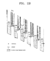
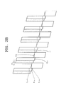
- FIGS. 2A and 2B are energy diagrams of the active region structure layer respectively showing the cases where a voltage is applied and is not applied to the interband tunneling intersubband transition semiconductor laser according to an embodiment of the present invention.
- the vertical axis represents the energy level and the horizontal axis represents the stack direction of the active region structure layer,
- each quantum well layer may be formed of a material having a small energy bandgap, such as InAs, InGaAsSb, or InAsSb.
- Each quantum barrier layer may be formed of a material having a relatively wide energy bandgap, such as GaSb or InGaSb. The quantum well and the quantum barrier layers are alternately stacked, thereby forming a heterostructure of InAsGaAlSb material system having a broken bandgap.
- the maximum energy level E V2 of a valence band of the quantum barrier layer is higher than the minimum energy level E C1 of a conduction band of the quantum well layer by band alignment of the quantum well and quantum barrier layers.
- the energy level difference between the energy levels may be 0.1 eV to 0.2 eV.
- E q1c2 and E q1c1 respectively denote a quantum confined upper electron state and a quantum confined lower electron state where a radiative transition of electrons occur in the quantum well layer"
- E q2v1 denotes a hole confined subband (or hole confined state) of the quantum barrier layer"
- the carriers having undergone the radiative transition to the quantum confined lower electron state E q1c1 are aligned with the hole confined state E q2v1 of a consecutive quantum barrier layer. Those carriers are reinjected to the quantum confined upper electron state E q1c2 of a consecutive quantum well layer by interband resonant tunneling.
- the population inversion between the quantum confined upper electron state E q1c2 and the quantum confined lower electron state E q1c1 causes a laser transition, thereby emitting a plurality of photons. That is, as one electron undergoes a series of the above processes while passing through the stack of N pairs of quantum well layers and quantum barrier layers, N photons are effectively generated.
- This structure is an injectorless structure, since it lacks an injector region of the conventional art, such as a multilayered Bragg reflector or an energy relaxation region between active regions.
- the injectorless structure allows a very thin and small intersubband transition semiconductor laser.
- the output wavelength of the semiconductor laser is determined by energy confinement states of a quantum well corresponding to laser transition levels of a quantum well layer.
- a quantum well layer may have a complex structure that has different minimum energy levels of a conduction band, or a quantum barrier layer may have a complex structure that has different maximum energy levels of a valence band, so that a design and output efficiency of an output wavelength of energy confinement states can be controlled.
- FIGS. 3 , 4 , 5 , 6 and 7 illustrate examples of a broken bandgap heterostructure in which quantum well layers and quantum barrier layers have a multilayered complex structure in the active region structure layer of FIG. 2 .
- FIGS. 3A and 3B are energy diagrams of a part of an active region structure layer respectively showing the cases where a voltage is and is not applied to an intersubband transition semiconductor laser according to another embodiment of the present invention.
- FIGS. 3A and 3B are energy diagrams of an example in which the quantum well layer of FIG., 2 includes a plurality of material layers, instead of a single material layer.
- a quantum well layer includes two material layers that have different respective minimum energy levels E C1 and E C3 of a conduction band.
- the maximum energy level E V2 of a valence band of a quantum barrier layer is greater than the higher level E C1 of the two minimum energy levels E C1 and E C3 of the conduction band of the quantum well layer.
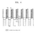
- FIG. 4 is an energy diagram of an active region structure layer of an example in which the quantum barrier layer of FIG. 2 includes a plurality of material layers, instead of including a single material layer.
- a quantum barrier layer includes two layers that have different respective maximum energy levels E V2 and E V4 of a valence band.
- the energy bandgap of a first quantum barrier material is smaller than that of a second quantum barrier material
- E V2 and E V4 respectively denote the maximum energy levels of the valence band of the two material layers of the quantum barrier layer
- E C2 and E C4 respectively denote the minimum energy levels of a conduction band thereof.
- E q1c2 and E q1c1 respectively denote a quantum confined upper electron state subband and a quantum confined lower electron state subband where a radiative transition of an electron occurs in the quantum well layer.
- E q2v1 denotes a hole confined subband of the quantum barrier layer.
- the quantum well layer and the quantum barrier layer are constructed such that interband resonant tunneling occurs due to alignment between the electron state E q1c1 of a quantum well layer and the hole state Eq 2v1 of a consecutive quantum barrier layer when an operation voltage is applied.
- FIG, 5 is an energy diagram of an example of a broken bandgap heterostructure employing a quantum well layer of FIG. 2 that has a complex structure including a plurality of material layers instead of a single material layer, and a quantum barrier layer of FIG. 2 that includes a plurality of material layers instead of a single material layer.
- a quantum well layer includes two material layers, and the energy bandgap of a first quantum well material layer is smaller than the energy bandgap of a second quantum well material layer.
- E V1 and E V3 respectively denote the maximum energy levels of the valence bands of two materials of the quantum well layer
- E C1 and E C3 respectively denote the minimum energy levels of the conduction bands of the two material layers.
- the quantum barrier layer also includes two material layers, and the energy bandgap of a first quantum barrier material layer is smaller than that of a second quantum barrier material layer.
- E V2 and E V4 respectively denote the valence-band maximum energy levels of the two material layers of the quantum barrier layer
- E C2 and E C4 respectively denote the conduction-band minimum energy levels of the two material layers of the quantum barrier layer.
- the valence-band maximum energy level of the quantum barrier layer is higher than the conduction-band minimum energy levels of the quantum well layer, thereby forming a broken bandgap heterostructure.
- E q1c2 and E q1c1 respectively denote a quantum confined upper electron state and a quantum confined lower electron state where a radiative transition of an electron occurs in the quantum well layer, and E q2v1 denotes a hole confined subband of the quantum barrier layer.
- the quantum well layer and the quantum barrier layer are constructed such that interband resonant tunneling occurs due to alignment between the electron state E q1c1 of the quantum well layer and the hole state E q2v1 of the consecutive quantum barrier layer structure when an operation voltage is applied.
- FIG. 6 is an energy diagram in the case where the quantum well layer of FIG. 2 includes three material layers instead of a single material layer, and the quantum barrier layer of FIG. 2 includes two material layers instead of a single material layer.
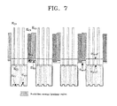
- FIG. 7 is an energy diagram in the case where the quantum well layer of FIG. 2 has a multi-quantum well structure instead of a single material layer, and the quantum barrier layer of FIG. 2 includes two material layers instead of a single material layer.
- Eq 1c2 and Eq 1c1 respectively denote a quantum confined upper electron state and a quantum confined lower electron state where a radiative transition of an electron occurs in the quantum well layer, and E q2v1 denotes a hole subband of the quantum barrier layer.
- the quantum well layer and the quantum barrier layer are constructed such that interband resonant tunneling occurs due to alignment between the electron state E q1c1 of the quantum well layer and the hole state E q2v1 of the consecutive quantum barrier layer when an operation voltage is applied.
- the quantum well layer has a complex structure having different minimum energy levels of a conduction band, or the quantum barrier layer has a complex structure having different maximum energy levels of a valence band, thereby forming a broken bandgap heterostructure. This allows energy confinement states to be controlled, so that the output wavelength, efficiency of power output, and device performance can be controlled.
Landscapes
- Physics & Mathematics (AREA)
- Optics & Photonics (AREA)
- Chemical & Material Sciences (AREA)
- Engineering & Computer Science (AREA)
- Nanotechnology (AREA)
- Condensed Matter Physics & Semiconductors (AREA)
- General Physics & Mathematics (AREA)
- Electromagnetism (AREA)
- Life Sciences & Earth Sciences (AREA)
- Biophysics (AREA)
- Crystallography & Structural Chemistry (AREA)
- Semiconductor Lasers (AREA)
Abstract
Description
- This application claims the benefit of
Korean Patent Application No. 10-2006-0125065, filed on December 8, 2006 - The present invention relates to an intersubband transition semiconductor laser, and more particularly, to an intersubband transition semiconductor layer capable of achieving a high output with an economical price, an easy manufacturing process, and a simple structure including a small number of stacked layers.
- Those skilled in the art have long predicted that a semiconductor superlattice structure may contribute to amplifying an electromagnetic wave to realize a unipolar intersubband transition quantum well semiconductor laser, and have made many efforts to develop the unipolar intersubband transition quantum well semiconductor laser.. This type of intersubband transition lasers have the advantages of a tailoring the frequency in the wide-range spectrum, a narrow line width based on the theoretical absence of line-width increasing factors, and low temperature-dependency of an oscillation threshold in comparison to a conventional bipolar semiconductor laser.
- A properly designed unipolar intersubband transition quantum well semiconductor laser may emit light having a submillimeter wavelength at a mid/far infrared ray. For example, light with a wavelength ranging from about 3 to 100 µm may be emitted by a carrier transition between quantum confinement states. The wavelength of light emitted may be designed with same heterostructure system over a wide spectrum range. The wavelength band cannot be obtained through a conventional semiconductor laser diode Also, the unipolar intersubband transition quantum well semiconductor laser can be manufactured on the basis of a sufficiently technically developed III-V compound semiconductor materials (e.g. a heterostructure based on GaAs or InP) which have relatively wide energy bandgaps. For this reason, there is no need to use a material with a small energy bandgap, which is sensitive to temperature and requires complex processes.
- Conventional technologies for implementing the unipolar intersubband transition quantum well semiconductor laser include a resonant tunneling structure based on a typical multiple quantum-well structure. For example, W. M. Yee et al. analyzed two kinds of coupled quantum well structures in "Carrier transport and intersubband population inversion in couple quantum well", Appl. Phys. Lett. 63(8), pp.1089-1091 (1993). Each of the coupled quantum well structures includes a quantum well for emission that is interposed between energy filter wells, coupled with a quantum well structure interposed between n-type doped injector/collector regions.
- In the year of 1994, Faist, Capasso, et al. named a unipolar intersubband transition quantum well semiconductor laser a quantum cascade LASER (QCL), and succeeded in the first emission of light with a wavelength of about 4.2 µm from a GalnAs/AllnAs material-based system. The laser that can be implemented with another material-based system can easily be designed to oscillate at a predetermined wavelength over a wide spectrum range
- The quantum cascade LASER includes an undoped multi-layered semiconductor quantum well structure as an active region. The quantum well active region is separated from a neighboring quantum well active region by an energy relaxation region. For example, a radiative transition between confinement energy states in the quantum well active region may be designed to be a vertical transition occurring in the same quantum well or a diagonal transition occurring between confinement energy states of neighboring quantum wells.
- The unipolar laser diode with such a wavelength band may be applied in a variety of fields such as contamination detection, process control, and automotive. Thus, the quantum cascade LASER that can emit mid/far infrared rays has received much commercial and scientific attention.
- However, in the conventional quantum cascade LASER, one electron emits N photons, while passing through N unit-cells stacked structures, where each unit cell includes tens of layers and have a quantum well active region and an energy relaxation region. To obtain a sufficient optical output, N must be about 25 to 70. For this reason, the structure is complicated and the manufacturing process is extremely difficult, since a multi-layered structure must be grown epitaxially using equipment such as a molecular beam epitaxy system. Thus, the conventional quantum cascade LASER has been studied and developed to an extremely limited extent.
- The present invention provides an interband resonant tunneling quantum semiconductor laser which can achieve a high optical power output with a simple, compact structure having a small number stack structure, can be easily manufactured, and uses an intersubband radiative transition and interband resonant tunneling in an active region of a semiconductor heterostructure.
- According to an aspect of the present invention, there is provided an intersubband transition semiconductor laser including a first cladding layer, an active region structure layer, and a second cladding layer that are formed on a semiconductor substrate, and upper and lower electrodes. The active region structure layer includes a plurality of quantum well layer/quantum barrier layer structures that are repetitively stacked on top of each other to allow an intersubband laser transition and interband resonant tunneling of injected carriers.
- This structure creates a broken-bandgap based semiconductor heterostructure in the active region structure layer, where an intersubband radiative transition occurs When an operation voltage is applied, carriers transited between laser energy states of a quantum well layer and undergo interband resonant tunneling through aligned electron-hole states of a consecutive quantum barrier layer. This improves the escape rate of the carriers from a laser transition lower state of the quantum well layer, and the injection efficiency of the carriers to the next quantum well layer, allowing efficient population inversion between laser transition states of the quantum well layer. Accordingly, there is provided an intersubband transition semiconductor laser that can achieve a high output with a simple compact structure including a small number of stacked layers, and can be easily manufactured
- An interband tunneling intersubband transition semiconductor laser according to the present invention is simple, compact, and cheap to manufacture, compared to a conventional quantum cascade laser having a complicated multilayered structure which makes manufacturing difficult,
- In the broken bandgap heterostructure, a quantum barrier layer includes a single material layer of a material having a relatively wide energy bandgap, such as GaSb or GalnSb, and may have a complex structure such as a superlattice structure, and a multiple quantum well structure based on a material system such as GaSb, GalnSb, or GaAlSb.
- In the broken bandgap heterostructure, a quantum well layer includes a single material layer of a material having a small energy bandgap such as InAs or InGaAsSb, and may have a complex structure such as a superlattice structure, and a multiple quantum well structure based on a material system such as InAs, AlSb, or InAlSb.
- When a voltage is applied to the electrodes, an intersubband transition and interband resonant tunneling of carriers occur consecutively in the active region structure layer. The intersubband transition and interband resonant tunneling may occur in a cascade mode.
- For example, in the case where InAs and GaSb constitute a heterostructure, a unique energy band alignment between the two materials allows the formation of a broken bandgap heterostructure, since the maximum energy level of a valence band of a GaSb quantum barrier layer is higher than the minimum energy of a conduction band of an InAs quantum well layer by about 0.15 eV. Also, the quantum resonant tunneling is an ultrafast-electron transfer phenomenon, and transfer efficiency of electrons is considerably increased by using this phenomenon
- In the heterostructure based on the InAs-GaSb material system, when an operation voltage is applied, interband resonant tunneling of carriers occurs from an electron state of the InAs quantum well layer to a hole state of the GaSb quantum barrier layer, and may help improve the efficiency of population inversion for an intersubband transition laser action of carriers in the quantum well layer.
- In the broken bandgap heterostructure, the quantum well layer and the quantum barrier layer each may include a single material layer, but may be a superlattice structure or a quantum well structure including a plurality of material layers.
- Optionally, the quantum well layer may include two material layers having different minimum energy levels of a conduction band, and the maximum energy level of a valence band of the quantum barrier layer may be higher than the higher of the minimum energy levels of the conduction bands of the two material layers
- Optionally, the quantum barrier layer may include two material layers having different maximum energy levels of a valence band, and the minimum energy level of a conduction band of the quantum well layer may be lower than the lower of the maximum energy levels of the valence bands of the two material layers.
- Optionally, the quantum well layer may include two material layers having different minimum energy levels of a conduction band, the quantum barrier layer may include two material layers having different maximum energy levels of a valence band, and the higher of the minimum energy levels of the conduction bands of the two material layers of the quantum well layer may be lower than the lower of the maximum energy levels of the valence bands of the two material layers of the quantum barrier layer.
- Optionally, the quantum well layer may include two material layers having different minimum energy levels of a conduction band, the quantum barrier layer may include three material layers, a middle material layer of the three material layers may have a maximum energy level of a valence band that is lower than the maximum energy levels of the valence bands of the other two materials, and the higher of the minimum energy levels of the conduction bands of the two material layers of the quantum well layer is lower than the lowest of the maximum energy levels of the valence bands of the three material layers of the quantum barrier layer..
- Optionally, the quantum barrier layer may include two material layers having different maximum energy levels of a valence band, the quantum well layer may include three material layers, a middle material layer of the three material layers may have a minimum energy level of a conduction band that is lower than the minimum energy levels of the conduction bands of the other two material layers, and the lower of the maximum energy levels of the valence bands of the two material layers of the quantum barrier layer is higher than the highest of the minimum energy levels of the conduction bands of the three material layers of the quantum well layer.
- The semiconductor laser of claim may further include a first waveguide layer between the first cladding layer and the active region structure layer, a second waveguide layer between the second cladding layer and the active region structure, and a buffer layer between the semiconductor substrate and the first cladding layer.
- The above and other features and advantages of the present invention will become more apparent by describing in detail exemplary embodiments thereof with reference to the attached drawings in which:
-
FIG. 1 is a side sectional view of an intersubband transition semiconductor laser according to an embodiment of the present invention; -
FIG. 2A through 7 are energy diagrams illustrating parts of active region structure layers in the cases where a voltage is applied or not applied to intersubband transition semiconductor lasers according to embodiments of the present invention - The present invention will now be described more fully with reference to the accompanying drawings, in which exemplary embodiments of the invention are shown. The invention may, however, be embodied in many different forms, and should not be construed as being limited to the embodiments set forth herein; rather, these embodiments are provided so that this disclosure will be thorough and complete, and will fully convey the concept of the invention to those skilled in the art. Like reference numerals denote like elements in the drawings, and thus their description will be omitted. Various elements and regions are illustrated schematically in the drawings. Thus, the present invention is not limited by relative sizes or intervals shown in the accompanying drawings. It will also be understood that when a layer is referred to as being "on" another layer or substrate, it can be directly on the other layer or substrate, or intervening layers may also be present.
- The present invention provides an interband tunneling intersubband transition semiconductor laser including a semiconductor substrate; a first cladding layer; an active region structure layer formed on the first cladding layer, and including quantum well layers and quantum barrier layers that are alternately stacked a plurality of times and have a broken bandgap energy; a second cladding layer; and electrodes under the semiconductor substrate and on the cladding layer.
-
FIG" 1 is a conceptual side-sectional view of an interband tunneling intersubband transition semiconductor laser according to an embodiment of the present invention. - A
buffer layer 170, afirst cladding layer 150b, afirst waveguide layer 160b, asecond waveguide layer 160a, and asecond cladding layer 150a are provided on asemiconductor substrate 120. - The
first cladding layer 150b may be placed between an activeregion structure layer 110 and anelectrode 130b. Also, thesecond cladding layer 150a may be placed between the activeregion structure layer 110 and anelectrode 130a. Thebuffer layer 170 may be placed between thefirst cladding layer 150b and theelectrode 130b. - Optionally, a contact layer (not shown) may be further provided between the
semiconductor substrate 120 and theelectrode 130b by impurity doping, in order to improve adhesion and ohmic contact between thesemiconductor substrate 120 and theelectrode 130b. Acontact layer 140 may be further provided between theelectrode 130a and thesecond cladding layer 150a by impurity doping. - The
second waveguide layer 160a may be provided between the activeregion structure layer 110 and thesecond cladding layer 150a, and thefirst waveguide layer 160b may be provided between the activeregion structure layer 110 and thefirst cladding layer 150b. - The active
region structure layer 110 includes quantum well layers 110a and quantum barrier layers 110b alternately stacked, thereby forming a broken bandgap heterostructure. - The
quantum well layer 110a may be formed of a single material with a small energy bandgap, such as InAs or InGaAsSb, or may have a complex structure such as a superlattice structure or a multiple quantum well structure based on a material system such as InAs, AlSb, or InAlSb. - The
quantum barrier layer 110b may be formed of a single material with a relatively wide energy bandgap, such as GaSb or GainSb, or may be a complex structure such as a superlattice structure or a multiple quantum well structure based on a material system such as GaSb, GalnSb, or GaAlSb" - The
electrodes semiconductor substrate 120 and on the activeregion structure layer 110. - When bias is applied to the
electrodes region structure layer 110. Particularly, the intersubband transition and the interband resonant tunneling may occur in a cascade mode. - The method of forming the
quantum well layer 110a and thequantum barrier layer 110b is not specifically limited. Examples include molecular beam epitaxy (MBE) and atomic layer deposition (ALD). These methods are well known to those skilled in the art, and thus the detailed description thereof will be omitted. -
FIGS. 2A and2B are energy diagrams of the active region structure layer respectively showing the cases where a voltage is applied and is not applied to the interband tunneling intersubband transition semiconductor laser according to an embodiment of the present invention. InFIGS. 2A and2B , the vertical axis represents the energy level and the horizontal axis represents the stack direction of the active region structure layer, - Here, each quantum well layer may be formed of a material having a small energy bandgap, such as InAs, InGaAsSb, or InAsSb. Each quantum barrier layer may be formed of a material having a relatively wide energy bandgap, such as GaSb or InGaSb. The quantum well and the quantum barrier layers are alternately stacked, thereby forming a heterostructure of InAsGaAlSb material system having a broken bandgap.
- As illustrated in
FIG. 2A , the maximum energy level EV2 of a valence band of the quantum barrier layer is higher than the minimum energy level EC1 of a conduction band of the quantum well layer by band alignment of the quantum well and quantum barrier layers. In the case of the broken bandgap heterostructure of the InAsGaAlSb material system, the energy level difference between the energy levels may be 0.1 eV to 0.2 eV. - In
FIG. 2A , Eq1c2 and Eq1c1 respectively denote a quantum confined upper electron state and a quantum confined lower electron state where a radiative transition of electrons occur in the quantum well layer" Eq2v1 denotes a hole confined subband (or hole confined state) of the quantum barrier layer" - When a voltage is applied to an electrode, the energy diagram of
FIG" 2A is changed as described inFIG. 2B . When a voltage is applied, carriers are injected to the quantum confined upper electron state Eq1c2 of the quantum well layer of the active region structure layer. After their lifetime Tq1c1 elapses, those carriers undergo a radiative transition to the quantum confined lower electron state (Eq1c1). In this process, photons are generated and radiated. - The carriers having undergone the radiative transition to the quantum confined lower electron state Eq1c1 are aligned with the hole confined state Eq2v1 of a consecutive quantum barrier layer. Those carriers are reinjected to the quantum confined upper electron state Eq1c2 of a consecutive quantum well layer by interband resonant tunneling.
- As illustrated in
FIG. 2B , carriers injected to the quantum confined upper electron state Eq1c2 are well confined because it is difficult for the carriers to pass through a consecutive quantum barrier, but the carriers which transition to the quantum confined lower electron state Eq1c1 are easily moved and reinjected to the quantum confined upper electron state of the next quantum well through the aligned hole confined state Eq2v1. This phenomenon consecutively occurs in each adjacent quantum well and quantum barrier layer. - This phenomenon consequently reduces the lifetime of carriers at the quantum confined lower electron state Eq1c1, compared to the lifetime of carriers at the quantum confined upper electron state Eq1c2, causing population inversion of carriers between both states. This improves an escape rate and injection efficiency to the next quantum well layer of the carriers,
- The population inversion between the quantum confined upper electron state Eq1c2 and the quantum confined lower electron state Eq1c1 causes a laser transition, thereby emitting a plurality of photons. That is, as one electron undergoes a series of the above processes while passing through the stack of N pairs of quantum well layers and quantum barrier layers, N photons are effectively generated.
- This structure is an injectorless structure, since it lacks an injector region of the conventional art, such as a multilayered Bragg reflector or an energy relaxation region between active regions. The injectorless structure allows a very thin and small intersubband transition semiconductor laser.
- The output wavelength of the semiconductor laser is determined by energy confinement states of a quantum well corresponding to laser transition levels of a quantum well layer.
- Also, a quantum well layer may have a complex structure that has different minimum energy levels of a conduction band, or a quantum barrier layer may have a complex structure that has different maximum energy levels of a valence band, so that a design and output efficiency of an output wavelength of energy confinement states can be controlled.
-
FIGS. 3 ,4 ,5 ,6 and7 illustrate examples of a broken bandgap heterostructure in which quantum well layers and quantum barrier layers have a multilayered complex structure in the active region structure layer ofFIG. 2 . -
FIGS. 3A and3B are energy diagrams of a part of an active region structure layer respectively showing the cases where a voltage is and is not applied to an intersubband transition semiconductor laser according to another embodiment of the present invention. -
FIGS. 3A and3B are energy diagrams of an example in which the quantum well layer ofFIG., 2 includes a plurality of material layers, instead of a single material layer. As illustrated inFIG. 3A , a quantum well layer includes two material layers that have different respective minimum energy levels EC1 and EC3 of a conduction band. - Also, as illustrated in
FIG. 3A , the maximum energy level EV2 of a valence band of a quantum barrier layer is greater than the higher level EC1 of the two minimum energy levels EC1 and EC3 of the conduction band of the quantum well layer. -
FIG. 4 is an energy diagram of an active region structure layer of an example in which the quantum barrier layer ofFIG. 2 includes a plurality of material layers, instead of including a single material layer. As illustrated inFIG. 4 , a quantum barrier layer includes two layers that have different respective maximum energy levels EV2 and EV4 of a valence band. InFIG. 4 , the energy bandgap of a first quantum barrier material is smaller than that of a second quantum barrier material" - In
FIG. 4 , EV2 and EV4 respectively denote the maximum energy levels of the valence band of the two material layers of the quantum barrier layer, and EC2 and EC4 respectively denote the minimum energy levels of a conduction band thereof. As the maximum energy levels of the valence band of the quantum barrier layer are higher than the minimum energy level EC1 of a conduction band of a quantum well layer, a broken bandgap heterostructure is formed. - Here, Eq1c2 and Eq1c1 respectively denote a quantum confined upper electron state subband and a quantum confined lower electron state subband where a radiative transition of an electron occurs in the quantum well layer. Eq2v1 denotes a hole confined subband of the quantum barrier layer. The quantum well layer and the quantum barrier layer are constructed such that interband resonant tunneling occurs due to alignment between the electron state Eq1c1 of a quantum well layer and the hole state Eq2v1 of a consecutive quantum barrier layer when an operation voltage is applied.
-
FIG, 5 is an energy diagram of an example of a broken bandgap heterostructure employing a quantum well layer ofFIG. 2 that has a complex structure including a plurality of material layers instead of a single material layer, and a quantum barrier layer ofFIG. 2 that includes a plurality of material layers instead of a single material layer. - In
FIG. 5 , a quantum well layer includes two material layers, and the energy bandgap of a first quantum well material layer is smaller than the energy bandgap of a second quantum well material layer.. EV1 and EV3 respectively denote the maximum energy levels of the valence bands of two materials of the quantum well layer, and EC1 and EC3 respectively denote the minimum energy levels of the conduction bands of the two material layers. - The quantum barrier layer also includes two material layers, and the energy bandgap of a first quantum barrier material layer is smaller than that of a second quantum barrier material layer. In
FIG. 5 , EV2 and EV4 respectively denote the valence-band maximum energy levels of the two material layers of the quantum barrier layer, and EC2 and EC4 respectively denote the conduction-band minimum energy levels of the two material layers of the quantum barrier layer. The valence-band maximum energy level of the quantum barrier layer is higher than the conduction-band minimum energy levels of the quantum well layer, thereby forming a broken bandgap heterostructure. - Eq1c2 and Eq1c1 respectively denote a quantum confined upper electron state and a quantum confined lower electron state where a radiative transition of an electron occurs in the quantum well layer, and Eq2v1 denotes a hole confined subband of the quantum barrier layer.
- The quantum well layer and the quantum barrier layer are constructed such that interband resonant tunneling occurs due to alignment between the electron state Eq1c1 of the quantum well layer and the hole state Eq2v1 of the consecutive quantum barrier layer structure when an operation voltage is applied.
-
FIG. 6 is an energy diagram in the case where the quantum well layer ofFIG. 2 includes three material layers instead of a single material layer, and the quantum barrier layer ofFIG. 2 includes two material layers instead of a single material layer. -
FIG. 7 is an energy diagram in the case where the quantum well layer ofFIG. 2 has a multi-quantum well structure instead of a single material layer, and the quantum barrier layer ofFIG. 2 includes two material layers instead of a single material layer. - Eq1c2 and Eq1c1 respectively denote a quantum confined upper electron state and a quantum confined lower electron state where a radiative transition of an electron occurs in the quantum well layer, and Eq2v1 denotes a hole subband of the quantum barrier layer.
- The quantum well layer and the quantum barrier layer are constructed such that interband resonant tunneling occurs due to alignment between the electron state Eq1c1 of the quantum well layer and the hole state Eq2v1 of the consecutive quantum barrier layer when an operation voltage is applied.
- As mentioned above, the quantum well layer has a complex structure having different minimum energy levels of a conduction band, or the quantum barrier layer has a complex structure having different maximum energy levels of a valence band, thereby forming a broken bandgap heterostructure. This allows energy confinement states to be controlled, so that the output wavelength, efficiency of power output, and device performance can be controlled.
- As described so far, according to the present invention, population inversion between laser transition states is efficiently achieved from a simple compact structure with a small number of stacked layers, so that an intersubband transition interband tunneling semiconductor laser with a simple structure can be easily manufactured, but still obtain high optical power output, especially compared to a conventional quantum cascade laser with a complicated multilayered structure and difficult manufacturing process. Accordingly, a subband transition semiconductor laser of a mid/far infrared ray band having a high optical power output with a low cost can be implemented.
- While the present invention has been particularly shown and described with reference to exemplary embodiments thereof, it will be understood by those of ordinary skill in the art that various changes in form and detail may be made therein without departing from the spirit and scope of the present invention as defined by the following claims.
Claims (12)
- An interband tunneling intersubband transition semiconductor laser comprising a first cladding layer, an active region structure layer, and a second cladding layer that are formed on a semiconductor substrate, and electrodes that are provided under the semiconductor substrate and above the second cladding layer respectively,
wherein the active region structure layer includes a quantum well layer and a quantum barrier layer that are stacked to have a heterostructure with broken bandgap energy, and allows interband tunneling to occur. - The semiconductor laser of claim 1, wherein in the active region structure layer, an intersubband transition and interband resonant tunneling of carriers consecutively occur when voltage is applied to the electrodes"
- The semiconductor laser of claim 1 or 2, wherein the quantum well layer includes at least one selected from the group consisting of InAs, InGaAsSb, InAs, AlSb, and InAlSb.
- The semiconductor laser of claim 1, 2 or 3, wherein the quantum barrier layer includes at least one selected from the group consisting of GaSb, GainSb, GaSb, GahSb, and GaAlSb.
- The semiconductor laser of claim 2, 3 or 4, wherein the intersubband transition and the interband resonant tunneling occur in a cascade mode.
- The semiconductor laser of one of claims 1 to 5, wherein each quantum well layer includes two material layers having different minimum energy levels of a conductive band, and
a maximum energy level of a valence band of the quantum barrier layer is higher than the higher of the minimum energy levels of the two material layers. - The semiconductor laser of one of claims 1 to 6, wherein each quantum barrier layer includes two material layers having different maximum energy levels of a valence band, and
a minimum energy level of a conduction band of the quantum well layer is lower than the lower of the maximum energy levels of the two material layers. - The semiconductor laser of one of claims 1 to 5, wherein the quantum well layer includes two material layers having different minimum energy levels of a conduction band,
the quantum barrier layer includes two material layers having different maximum energy levels of a valence band, and
the higher of the minimum energy levels of the conduction bands of the two material layers of the quantum well layer is lower than the lower of the maximum energy levels of the valence bands of the two material layers of the quantum barrier layer. - The semiconductor laser of one of claims 1 to 5, wherein the quantum well layer includes two material layers having different minimum energy levels of a conduction band,
the quantum barrier layer includes three material layers, wherein a middle material layer of the three material layers has a maximum energy level of a valence band that is lower than maximum energy levels of the valence bands of the other two materials, and
the higher of the minimum energy levels of the conduction bands of the two material layers of the quantum well layer is lower than the lowest of the maximum energy levels of the valence bands of the three material layers of the quantum barrier layer. - The semiconductor laser of one of claims 1 to 5, wherein the quantum barrier layer includes two material layers having different maximum energy levels of a valence band,
the quantum well layer includes three material layers, wherein a middle material layer of the three material layers has a minimum energy level of a conduction band that is lower than minimum energy levels of the conduction bands of the other two material layers, and
the lower of the maximum energy levels of the valence bands of the two material layers of the quantum barrier layer is higher than the highest of the minimum energy levels of the conduction bands of the three material layers of the quantum well layer. - The semiconductor laser of one of claims 1 to 5, wherein the quantum well layer includes a complex structure such as a multi quantum well structure or a superlattice structure.
- The semiconductor laser of one of claims 1 to 11, further comprising:a first waveguide layer between the first cladding layer and the active region structure layer;a second waveguide layer between the second cladding layer and the active region structure; anda buffer layer between the semiconductor substrate and the first cladding layer.
Applications Claiming Priority (1)
| Application Number | Priority Date | Filing Date | Title |
|---|---|---|---|
| KR1020060125065A KR100842288B1 (en) | 2006-12-08 | 2006-12-08 | Interband Tunneling Subband Transition Semiconductor Laser |
Publications (3)
| Publication Number | Publication Date |
|---|---|
| EP1931001A2 true EP1931001A2 (en) | 2008-06-11 |
| EP1931001A3 EP1931001A3 (en) | 2010-03-10 |
| EP1931001B1 EP1931001B1 (en) | 2011-03-30 |
Family
ID=39156620
Family Applications (1)
| Application Number | Title | Priority Date | Filing Date |
|---|---|---|---|
| EP07122624A Not-in-force EP1931001B1 (en) | 2006-12-08 | 2007-12-07 | Interband tunneling intersubband transition semiconductor laser |
Country Status (5)
| Country | Link |
|---|---|
| US (1) | US7756176B2 (en) |
| EP (1) | EP1931001B1 (en) |
| KR (1) | KR100842288B1 (en) |
| AT (1) | ATE504106T1 (en) |
| DE (1) | DE602007013518D1 (en) |
Families Citing this family (4)
| Publication number | Priority date | Publication date | Assignee | Title |
|---|---|---|---|---|
| US8325774B2 (en) * | 2010-08-12 | 2012-12-04 | Wisconsin Alumni Research Foundation | High power, high efficiency quantum cascade lasers with reduced electron leakage |
| EP2803122B1 (en) * | 2012-01-13 | 2020-06-10 | Thorlabs Quantum Electronics, Inc. | Mid-ir multiwavelength concatenated distributed-feedback laser with an active core made of cascaded stages |
| US9209288B2 (en) * | 2012-12-21 | 2015-12-08 | Intel Corporation | Reduced scale resonant tunneling field effect transistor |
| US20160211393A1 (en) * | 2015-01-16 | 2016-07-21 | The Government Of The United States Of America, As Represented By The Secretary Of The Navy | Tunnel Diode With Broken-Gap Quantum Well |
Family Cites Families (14)
| Publication number | Priority date | Publication date | Assignee | Title |
|---|---|---|---|---|
| US5509025A (en) | 1994-04-04 | 1996-04-16 | At&T Corp. | Unipolar semiconductor laser |
| US5457709A (en) | 1994-04-04 | 1995-10-10 | At&T Ipm Corp. | Unipolar semiconductor laser |
| US5570386A (en) | 1994-04-04 | 1996-10-29 | Lucent Technologies Inc. | Semiconductor laser |
| US5588015A (en) * | 1995-08-22 | 1996-12-24 | University Of Houston | Light emitting devices based on interband transitions in type-II quantum well heterostructures |
| US5727010A (en) | 1996-03-20 | 1998-03-10 | Lucent Technologies Inc. | Article comprising an improved quantum cascade laser |
| US5799026A (en) * | 1996-11-01 | 1998-08-25 | The United States Of America As Represented By The Secretary Of The Navy | Interband quantum well cascade laser, with a blocking quantum well for improved quantum efficiency |
| US5936989A (en) | 1997-04-29 | 1999-08-10 | Lucent Technologies, Inc. | Quantum cascade laser |
| US5745516A (en) | 1996-11-06 | 1998-04-28 | Lucent Technologies Inc. | Article comprising a unipolar superlattice laser |
| GB9704987D0 (en) * | 1997-03-11 | 1997-04-30 | Isis Innovation | Infrared radiation source |
| JP2001077466A (en) | 1999-09-03 | 2001-03-23 | Rohm Co Ltd | Semiconductor laser |
| JP3412007B2 (en) * | 1999-09-03 | 2003-06-03 | 東北大学長 | Light emitting element between sub-bands |
| US6556604B1 (en) | 2000-11-08 | 2003-04-29 | Lucent Technologies Inc. | Flat minibands with spatially symmetric wavefunctions in intersubband superlattice light emitters |
| JP2003046125A (en) | 2001-07-30 | 2003-02-14 | Shin Etsu Handotai Co Ltd | Light emitting element |
| JP3857295B2 (en) * | 2004-11-10 | 2006-12-13 | 三菱電機株式会社 | Semiconductor light emitting device |
-
2006
- 2006-12-08 KR KR1020060125065A patent/KR100842288B1/en not_active Expired - Fee Related
-
2007
- 2007-12-07 EP EP07122624A patent/EP1931001B1/en not_active Not-in-force
- 2007-12-07 US US11/952,408 patent/US7756176B2/en not_active Expired - Fee Related
- 2007-12-07 AT AT07122624T patent/ATE504106T1/en not_active IP Right Cessation
- 2007-12-07 DE DE602007013518T patent/DE602007013518D1/en active Active
Non-Patent Citations (2)
| Title |
|---|
| FAIST; CAPASSO ET AL.: "named a unipolar intersubband transition quantum well semiconductor laser a quantum cascade", LASER (QCL, 1994 |
| W. M. YEE ET AL.: "analyzed two kinds of coupled quantum well structures in "Carrier transport and intersubband population inversion in couple quantum well"", APPT. PHYS. LETT., vol. 63, no. 8, 1993, pages 1089 - 1091 |
Also Published As
| Publication number | Publication date |
|---|---|
| US7756176B2 (en) | 2010-07-13 |
| KR20080053094A (en) | 2008-06-12 |
| KR100842288B1 (en) | 2008-06-30 |
| EP1931001B1 (en) | 2011-03-30 |
| DE602007013518D1 (en) | 2011-05-12 |
| US20080151956A1 (en) | 2008-06-26 |
| ATE504106T1 (en) | 2011-04-15 |
| EP1931001A3 (en) | 2010-03-10 |
Similar Documents
| Publication | Publication Date | Title |
|---|---|---|
| Fox et al. | Quantum wells, superlattices, and band-gap engineering | |
| Vurgaftman et al. | Interband cascade lasers | |
| US7227173B2 (en) | Semiconductor devices and methods | |
| US7856042B2 (en) | High efficiency intersubband semiconductor lasers | |
| US8068528B2 (en) | Quantum cascade laser | |
| US5588015A (en) | Light emitting devices based on interband transitions in type-II quantum well heterostructures | |
| US7558305B2 (en) | Intersubband mid-infrared electroluminescent semiconductor devices | |
| EP2249444B1 (en) | Quantum cascade laser | |
| US6148012A (en) | Multiple wavelength quantum cascade light source | |
| US20080259983A1 (en) | Semiconductor quantum cascade laser and systems and methods for manufacturing the same | |
| EP1931001B1 (en) | Interband tunneling intersubband transition semiconductor laser | |
| JPH0653602A (en) | Semiconductor laser device | |
| JP2004119814A (en) | Unipolar multiple quantum well device and manufacturing method thereof | |
| US20130121361A1 (en) | Interband Cascade Laser Amplifier Medium | |
| US6819696B1 (en) | Intersubband semiconductor lasers with enhanced subband depopulation rate | |
| KR100818632B1 (en) | Subband Transition Semiconductor Laser | |
| WO2015159630A1 (en) | Semiconductor laser | |
| Unger | Semiconductor lasers | |
| Kurtz et al. | Infrared emitting device and method | |
| KR20070071397A (en) | Structure of laser diode |
Legal Events
| Date | Code | Title | Description |
|---|---|---|---|
| PUAI | Public reference made under article 153(3) epc to a published international application that has entered the european phase |
Free format text: ORIGINAL CODE: 0009012 |
|
| AK | Designated contracting states |
Kind code of ref document: A2 Designated state(s): AT BE BG CH CY CZ DE DK EE ES FI FR GB GR HU IE IS IT LI LT LU LV MC MT NL PL PT RO SE SI SK TR |
|
| AX | Request for extension of the european patent |
Extension state: AL BA HR MK RS |
|
| PUAL | Search report despatched |
Free format text: ORIGINAL CODE: 0009013 |
|
| AK | Designated contracting states |
Kind code of ref document: A3 Designated state(s): AT BE BG CH CY CZ DE DK EE ES FI FR GB GR HU IE IS IT LI LT LU LV MC MT NL PL PT RO SE SI SK TR |
|
| AX | Request for extension of the european patent |
Extension state: AL BA HR MK RS |
|
| 17P | Request for examination filed |
Effective date: 20100910 |
|
| GRAP | Despatch of communication of intention to grant a patent |
Free format text: ORIGINAL CODE: EPIDOSNIGR1 |
|
| AKX | Designation fees paid |
Designated state(s): AT BE BG CH CY CZ DE DK EE ES FI FR GB GR HU IE IS IT LI LT LU LV MC MT NL PL PT RO SE SI SK TR |
|
| GRAS | Grant fee paid |
Free format text: ORIGINAL CODE: EPIDOSNIGR3 |
|
| GRAA | (expected) grant |
Free format text: ORIGINAL CODE: 0009210 |
|
| AK | Designated contracting states |
Kind code of ref document: B1 Designated state(s): AT BE BG CH CY CZ DE DK EE ES FI FR GB GR HU IE IS IT LI LT LU LV MC MT NL PL PT RO SE SI SK TR |
|
| REG | Reference to a national code |
Ref country code: GB Ref legal event code: FG4D |
|
| REG | Reference to a national code |
Ref country code: CH Ref legal event code: EP |
|
| REG | Reference to a national code |
Ref country code: IE Ref legal event code: FG4D |
|
| REG | Reference to a national code |
Ref country code: CH Ref legal event code: NV Representative=s name: RENTSCH & PARTNER |
|
| REF | Corresponds to: |
Ref document number: 602007013518 Country of ref document: DE Date of ref document: 20110512 Kind code of ref document: P |
|
| REG | Reference to a national code |
Ref country code: DE Ref legal event code: R096 Ref document number: 602007013518 Country of ref document: DE Effective date: 20110512 |
|
| REG | Reference to a national code |
Ref country code: CH Ref legal event code: PFA Owner name: ELECTRONICS AND TELECOMMUNICATIONS RESEARCH INSTI Free format text: ELECTRONICS AND TELECOMMUNICATIONS RESEARCH INSTITUTE#161 GAJEONG-DONG YUSEONG-GU#DAEJEON (KR) -TRANSFER TO- ELECTRONICS AND TELECOMMUNICATIONS RESEARCH INSTITUTE#161 GAJEONG-DONG YUSEONG-GU#DAEJEON (KR) |
|
| REG | Reference to a national code |
Ref country code: NL Ref legal event code: VDEP Effective date: 20110330 |
|
| PG25 | Lapsed in a contracting state [announced via postgrant information from national office to epo] |
Ref country code: LT Free format text: LAPSE BECAUSE OF FAILURE TO SUBMIT A TRANSLATION OF THE DESCRIPTION OR TO PAY THE FEE WITHIN THE PRESCRIBED TIME-LIMIT Effective date: 20110330 Ref country code: GR Free format text: LAPSE BECAUSE OF FAILURE TO SUBMIT A TRANSLATION OF THE DESCRIPTION OR TO PAY THE FEE WITHIN THE PRESCRIBED TIME-LIMIT Effective date: 20110701 Ref country code: LV Free format text: LAPSE BECAUSE OF FAILURE TO SUBMIT A TRANSLATION OF THE DESCRIPTION OR TO PAY THE FEE WITHIN THE PRESCRIBED TIME-LIMIT Effective date: 20110330 Ref country code: SE Free format text: LAPSE BECAUSE OF FAILURE TO SUBMIT A TRANSLATION OF THE DESCRIPTION OR TO PAY THE FEE WITHIN THE PRESCRIBED TIME-LIMIT Effective date: 20110330 |
|
| LTIE | Lt: invalidation of european patent or patent extension |
Effective date: 20110330 |
|
| PG25 | Lapsed in a contracting state [announced via postgrant information from national office to epo] |
Ref country code: FI Free format text: LAPSE BECAUSE OF FAILURE TO SUBMIT A TRANSLATION OF THE DESCRIPTION OR TO PAY THE FEE WITHIN THE PRESCRIBED TIME-LIMIT Effective date: 20110330 Ref country code: SI Free format text: LAPSE BECAUSE OF FAILURE TO SUBMIT A TRANSLATION OF THE DESCRIPTION OR TO PAY THE FEE WITHIN THE PRESCRIBED TIME-LIMIT Effective date: 20110330 Ref country code: AT Free format text: LAPSE BECAUSE OF FAILURE TO SUBMIT A TRANSLATION OF THE DESCRIPTION OR TO PAY THE FEE WITHIN THE PRESCRIBED TIME-LIMIT Effective date: 20110330 Ref country code: CY Free format text: LAPSE BECAUSE OF FAILURE TO SUBMIT A TRANSLATION OF THE DESCRIPTION OR TO PAY THE FEE WITHIN THE PRESCRIBED TIME-LIMIT Effective date: 20110330 |
|
| PG25 | Lapsed in a contracting state [announced via postgrant information from national office to epo] |
Ref country code: BE Free format text: LAPSE BECAUSE OF FAILURE TO SUBMIT A TRANSLATION OF THE DESCRIPTION OR TO PAY THE FEE WITHIN THE PRESCRIBED TIME-LIMIT Effective date: 20110330 |
|
| PG25 | Lapsed in a contracting state [announced via postgrant information from national office to epo] |
Ref country code: PT Free format text: LAPSE BECAUSE OF FAILURE TO SUBMIT A TRANSLATION OF THE DESCRIPTION OR TO PAY THE FEE WITHIN THE PRESCRIBED TIME-LIMIT Effective date: 20110801 Ref country code: EE Free format text: LAPSE BECAUSE OF FAILURE TO SUBMIT A TRANSLATION OF THE DESCRIPTION OR TO PAY THE FEE WITHIN THE PRESCRIBED TIME-LIMIT Effective date: 20110330 |
|
| PG25 | Lapsed in a contracting state [announced via postgrant information from national office to epo] |
Ref country code: RO Free format text: LAPSE BECAUSE OF FAILURE TO SUBMIT A TRANSLATION OF THE DESCRIPTION OR TO PAY THE FEE WITHIN THE PRESCRIBED TIME-LIMIT Effective date: 20110330 Ref country code: IS Free format text: LAPSE BECAUSE OF FAILURE TO SUBMIT A TRANSLATION OF THE DESCRIPTION OR TO PAY THE FEE WITHIN THE PRESCRIBED TIME-LIMIT Effective date: 20110730 Ref country code: SK Free format text: LAPSE BECAUSE OF FAILURE TO SUBMIT A TRANSLATION OF THE DESCRIPTION OR TO PAY THE FEE WITHIN THE PRESCRIBED TIME-LIMIT Effective date: 20110330 Ref country code: CZ Free format text: LAPSE BECAUSE OF FAILURE TO SUBMIT A TRANSLATION OF THE DESCRIPTION OR TO PAY THE FEE WITHIN THE PRESCRIBED TIME-LIMIT Effective date: 20110330 Ref country code: ES Free format text: LAPSE BECAUSE OF FAILURE TO SUBMIT A TRANSLATION OF THE DESCRIPTION OR TO PAY THE FEE WITHIN THE PRESCRIBED TIME-LIMIT Effective date: 20110711 |
|
| PG25 | Lapsed in a contracting state [announced via postgrant information from national office to epo] |
Ref country code: NL Free format text: LAPSE BECAUSE OF FAILURE TO SUBMIT A TRANSLATION OF THE DESCRIPTION OR TO PAY THE FEE WITHIN THE PRESCRIBED TIME-LIMIT Effective date: 20110330 |
|
| PGFP | Annual fee paid to national office [announced via postgrant information from national office to epo] |
Ref country code: CH Payment date: 20111107 Year of fee payment: 5 |
|
| PLBE | No opposition filed within time limit |
Free format text: ORIGINAL CODE: 0009261 |
|
| STAA | Information on the status of an ep patent application or granted ep patent |
Free format text: STATUS: NO OPPOSITION FILED WITHIN TIME LIMIT |
|
| PG25 | Lapsed in a contracting state [announced via postgrant information from national office to epo] |
Ref country code: PL Free format text: LAPSE BECAUSE OF FAILURE TO SUBMIT A TRANSLATION OF THE DESCRIPTION OR TO PAY THE FEE WITHIN THE PRESCRIBED TIME-LIMIT Effective date: 20110330 Ref country code: DK Free format text: LAPSE BECAUSE OF FAILURE TO SUBMIT A TRANSLATION OF THE DESCRIPTION OR TO PAY THE FEE WITHIN THE PRESCRIBED TIME-LIMIT Effective date: 20110330 |
|
| 26N | No opposition filed |
Effective date: 20120102 |
|
| REG | Reference to a national code |
Ref country code: DE Ref legal event code: R097 Ref document number: 602007013518 Country of ref document: DE Effective date: 20120102 |
|
| PG25 | Lapsed in a contracting state [announced via postgrant information from national office to epo] |
Ref country code: IT Free format text: LAPSE BECAUSE OF FAILURE TO SUBMIT A TRANSLATION OF THE DESCRIPTION OR TO PAY THE FEE WITHIN THE PRESCRIBED TIME-LIMIT Effective date: 20110330 |
|
| PG25 | Lapsed in a contracting state [announced via postgrant information from national office to epo] |
Ref country code: MC Free format text: LAPSE BECAUSE OF NON-PAYMENT OF DUE FEES Effective date: 20111231 |
|
| GBPC | Gb: european patent ceased through non-payment of renewal fee |
Effective date: 20111207 |
|
| REG | Reference to a national code |
Ref country code: FR Ref legal event code: ST Effective date: 20120831 |
|
| REG | Reference to a national code |
Ref country code: IE Ref legal event code: MM4A |
|
| REG | Reference to a national code |
Ref country code: DE Ref legal event code: R119 Ref document number: 602007013518 Country of ref document: DE Effective date: 20120703 |
|
| PG25 | Lapsed in a contracting state [announced via postgrant information from national office to epo] |
Ref country code: DE Free format text: LAPSE BECAUSE OF NON-PAYMENT OF DUE FEES Effective date: 20120703 Ref country code: IE Free format text: LAPSE BECAUSE OF NON-PAYMENT OF DUE FEES Effective date: 20111207 Ref country code: GB Free format text: LAPSE BECAUSE OF NON-PAYMENT OF DUE FEES Effective date: 20111207 |
|
| PG25 | Lapsed in a contracting state [announced via postgrant information from national office to epo] |
Ref country code: MT Free format text: LAPSE BECAUSE OF FAILURE TO SUBMIT A TRANSLATION OF THE DESCRIPTION OR TO PAY THE FEE WITHIN THE PRESCRIBED TIME-LIMIT Effective date: 20110330 |
|
| PG25 | Lapsed in a contracting state [announced via postgrant information from national office to epo] |
Ref country code: FR Free format text: LAPSE BECAUSE OF NON-PAYMENT OF DUE FEES Effective date: 20120102 |
|
| PG25 | Lapsed in a contracting state [announced via postgrant information from national office to epo] |
Ref country code: LU Free format text: LAPSE BECAUSE OF NON-PAYMENT OF DUE FEES Effective date: 20111207 |
|
| PG25 | Lapsed in a contracting state [announced via postgrant information from national office to epo] |
Ref country code: BG Free format text: LAPSE BECAUSE OF FAILURE TO SUBMIT A TRANSLATION OF THE DESCRIPTION OR TO PAY THE FEE WITHIN THE PRESCRIBED TIME-LIMIT Effective date: 20110630 |
|
| REG | Reference to a national code |
Ref country code: CH Ref legal event code: PL |
|
| PG25 | Lapsed in a contracting state [announced via postgrant information from national office to epo] |
Ref country code: TR Free format text: LAPSE BECAUSE OF FAILURE TO SUBMIT A TRANSLATION OF THE DESCRIPTION OR TO PAY THE FEE WITHIN THE PRESCRIBED TIME-LIMIT Effective date: 20110330 |
|
| PG25 | Lapsed in a contracting state [announced via postgrant information from national office to epo] |
Ref country code: HU Free format text: LAPSE BECAUSE OF FAILURE TO SUBMIT A TRANSLATION OF THE DESCRIPTION OR TO PAY THE FEE WITHIN THE PRESCRIBED TIME-LIMIT Effective date: 20110330 Ref country code: CH Free format text: LAPSE BECAUSE OF NON-PAYMENT OF DUE FEES Effective date: 20121231 Ref country code: LI Free format text: LAPSE BECAUSE OF NON-PAYMENT OF DUE FEES Effective date: 20121231 |