EP1930939A2 - Two step etching of a bottom anti-reflective coating layer in dual damascene application - Google Patents
Two step etching of a bottom anti-reflective coating layer in dual damascene application Download PDFInfo
- Publication number
- EP1930939A2 EP1930939A2 EP07122597A EP07122597A EP1930939A2 EP 1930939 A2 EP1930939 A2 EP 1930939A2 EP 07122597 A EP07122597 A EP 07122597A EP 07122597 A EP07122597 A EP 07122597A EP 1930939 A2 EP1930939 A2 EP 1930939A2
- Authority
- EP
- European Patent Office
- Prior art keywords
- gas mixture
- supplying
- gas
- etching
- etch
- Prior art date
- Legal status (The legal status is an assumption and is not a legal conclusion. Google has not performed a legal analysis and makes no representation as to the accuracy of the status listed.)
- Withdrawn
Links
Images



Classifications
-
- H—ELECTRICITY
- H10—SEMICONDUCTOR DEVICES; ELECTRIC SOLID-STATE DEVICES NOT OTHERWISE PROVIDED FOR
- H10P—GENERIC PROCESSES OR APPARATUS FOR THE MANUFACTURE OR TREATMENT OF DEVICES COVERED BY CLASS H10
- H10P50/00—Etching of wafers, substrates or parts of devices
- H10P50/20—Dry etching; Plasma etching; Reactive-ion etching
- H10P50/24—Dry etching; Plasma etching; Reactive-ion etching of semiconductor materials
- H10P50/242—Dry etching; Plasma etching; Reactive-ion etching of semiconductor materials of Group IV materials
-
- H—ELECTRICITY
- H10—SEMICONDUCTOR DEVICES; ELECTRIC SOLID-STATE DEVICES NOT OTHERWISE PROVIDED FOR
- H10P—GENERIC PROCESSES OR APPARATUS FOR THE MANUFACTURE OR TREATMENT OF DEVICES COVERED BY CLASS H10
- H10P70/00—Cleaning of wafers, substrates or parts of devices
- H10P70/20—Cleaning during device manufacture
- H10P70/23—Cleaning during device manufacture during, before or after processing of insulating materials
- H10P70/234—Cleaning during device manufacture during, before or after processing of insulating materials the processing being the formation of vias or contact holes
-
- H—ELECTRICITY
- H10—SEMICONDUCTOR DEVICES; ELECTRIC SOLID-STATE DEVICES NOT OTHERWISE PROVIDED FOR
- H10D—INORGANIC ELECTRIC SEMICONDUCTOR DEVICES
- H10D64/00—Electrodes of devices having potential barriers
- H10D64/01—Manufacture or treatment
- H10D64/011—Manufacture or treatment of electrodes ohmically coupled to a semiconductor
-
- H—ELECTRICITY
- H10—SEMICONDUCTOR DEVICES; ELECTRIC SOLID-STATE DEVICES NOT OTHERWISE PROVIDED FOR
- H10P—GENERIC PROCESSES OR APPARATUS FOR THE MANUFACTURE OR TREATMENT OF DEVICES COVERED BY CLASS H10
- H10P50/00—Etching of wafers, substrates or parts of devices
- H10P50/20—Dry etching; Plasma etching; Reactive-ion etching
- H10P50/28—Dry etching; Plasma etching; Reactive-ion etching of insulating materials
- H10P50/282—Dry etching; Plasma etching; Reactive-ion etching of insulating materials of inorganic materials
- H10P50/283—Dry etching; Plasma etching; Reactive-ion etching of insulating materials of inorganic materials by chemical means
-
- H—ELECTRICITY
- H10—SEMICONDUCTOR DEVICES; ELECTRIC SOLID-STATE DEVICES NOT OTHERWISE PROVIDED FOR
- H10P—GENERIC PROCESSES OR APPARATUS FOR THE MANUFACTURE OR TREATMENT OF DEVICES COVERED BY CLASS H10
- H10P50/00—Etching of wafers, substrates or parts of devices
- H10P50/20—Dry etching; Plasma etching; Reactive-ion etching
- H10P50/28—Dry etching; Plasma etching; Reactive-ion etching of insulating materials
- H10P50/286—Dry etching; Plasma etching; Reactive-ion etching of insulating materials of organic materials
- H10P50/287—Dry etching; Plasma etching; Reactive-ion etching of insulating materials of organic materials by chemical means
-
- H—ELECTRICITY
- H10—SEMICONDUCTOR DEVICES; ELECTRIC SOLID-STATE DEVICES NOT OTHERWISE PROVIDED FOR
- H10P—GENERIC PROCESSES OR APPARATUS FOR THE MANUFACTURE OR TREATMENT OF DEVICES COVERED BY CLASS H10
- H10P50/00—Etching of wafers, substrates or parts of devices
- H10P50/73—Etching of wafers, substrates or parts of devices using masks for insulating materials
-
- H—ELECTRICITY
- H10—SEMICONDUCTOR DEVICES; ELECTRIC SOLID-STATE DEVICES NOT OTHERWISE PROVIDED FOR
- H10W—GENERIC PACKAGES, INTERCONNECTIONS, CONNECTORS OR OTHER CONSTRUCTIONAL DETAILS OF DEVICES COVERED BY CLASS H10
- H10W20/00—Interconnections in chips, wafers or substrates
- H10W20/01—Manufacture or treatment
- H10W20/071—Manufacture or treatment of dielectric parts thereof
- H10W20/081—Manufacture or treatment of dielectric parts thereof by forming openings in the dielectric parts
- H10W20/084—Manufacture or treatment of dielectric parts thereof by forming openings in the dielectric parts for dual-damascene structures
- H10W20/085—Manufacture or treatment of dielectric parts thereof by forming openings in the dielectric parts for dual-damascene structures involving intermediate temporary filling with material
Definitions
- the present invention generally relates to semiconductor processing technologies and, more specifically, to methods for etching a bottom anti-reflective coating (BARC) layer in a dual damascene etching process.
- BARC bottom anti-reflective coating
- Integrated circuits have evolved into complex devices that can include millions of components (e.g., transistors, capacitors and resistors) on a single chip.
- components e.g., transistors, capacitors and resistors
- the evolution of chip designs continually requires faster circuitry and greater circuit density.
- the demands for greater circuit density necessitate a reduction in the dimensions of the integrated circuit components.
- metal interconnects with low resistance provide conductive paths between the components on integrated circuits.
- Copper is particularly advantageous for use in interconnect structures due to its desirable electrical properties.
- Copper interconnect system are typically fabricated using a damascene process in which trenches and vias are etched into dielectric layers. The trenches and vias are filled with copper which is then planarized using, for example, a chemical-mechanical planarization (CMP) process.
- CMP chemical-mechanical planarization
- Copper interconnects are electrically isolated from each other by an insulating material.
- capacitive coupling may potentially occur between such interconnects. Capacitive coupling between adjacent metal interconnects may cause cross talk and/or resistance-capacitance (RC) delay which degrades the overall performance of the integrated circuit.
- RC resistance-capacitance
- low dielectric constant (low k) insulating materials e.g. dielectric constants less than about 4.0
- Figures 1A-1D illustrate an exemplary dual damascene structure formed by a "via-first" processing sequence.
- a dielectric bulk insulating layer 110 and an underlying dielectric barrier layer 108 are stacked on another previously formed interconnect having a conductive layer 106 embedded in another dielectric bulk insulating layer 104 disposed on a substrate 102.
- An optional polish stop layer or anti-reflective coating (ARC) 112 may be disposed on the dielectric bulk insulating layer 110.
- the dielectric bulk insulating layer 110 is typically formed from a dielectric material having a dielectric constant lower than 4.0, such as FSG, polymer material, carbon containing silicon layer (SiOC), and the like.
- a bottom anti-reflective coating (BARC) layer 114 is spin-applied to fill vias 128 formed by a via etching process and covers dielectric bulk insulating layer 110 before trench lithography.
- a photoresist layer 116 is disposed on the BARC layer 114 and patterned to define an opening 130 for forming trenches.
- a BARC etching process is performed to clear away a portion of the BARC layer 114 over the via opening 128 masked by the patterned photoresist layer 116 before etching the trenches, as shown in Figure 1B .
- the BARC etching process is performed until the optional polish stop layer 112 defined by the photoresist layer 116 is exposed and the BARC layer 114 filling the via 128 is etched to a predetermined depth, as shown in Figure 1B .
- a trench etching process is performed to etch the exposed polish stop layer 112 and the underlying dielectric bulk insulating layer 110 defined by the patterned photoresist layer 116, as shown in Figure 1C .
- the trench etching process etches the dielectric bulk insulating layer 110 into a predetermined depth and defines trenches 122 in the dielectric bulk insulating layer 110.
- the remaining BARC layer 114 filling the via 128 and the photoresist layer 116 on the top surface of the dielectric bulk insulating layer 110 are removed from the substrate 102, thereby forming dual damascene structure on the substrate 102, as shown in Figure 1D .
- an oxygen containing plasma etch process is performed to react with the remaining BARC layer 114 and the photoresist layer 116 on the substrate 102, forming a carbon oxide polymer which is pumped out of the processing chamber.
- oxygen present plasma during the removal of BARC layer 114 and photoresist layer 116 may attack the exposed sidewall 120 and surface 126 of the trenches 122 and/or vias 128 formed in the dielectric bulk insulating layer 110.
- Oxygen may form a Si-O bond on the surface of the dielectric bulk insulating layer 110, which adversely affect the dielectric properties of the dielectric bulk insulating layer 110.
- oxygen may accumulate on the sidewall 120 or exposed surface 126 of the low-k dielectric bulk insulating layer 110, and penetrate into the porous low-k dielectrics, thereby causing the carbon depletion at the film surface.
- Carbon depletion may cause the dielectric constant of the low-k material to undesirably increase, resulting in a "k loss" of the material dielectric properties.
- cross-talk and RC delay may increase after the BARC and photoresist etching process.
- removal of the BARC and/or photoresist layer removal process may also leave contaminants 124, such as residual BARC, residual photoresist layer, impurities, organic or inorganic byproducts in the vias 128 and/or trenches 122.
- contaminants 124 present in the vias 128 and/or trenches 122 may adversely effect the overall integration of the interconnection structure, resulting in poor device reliability and electrical performance.
- the method includes providing a substrate having a feature filled with a BARC layer in an etching chamber, supplying a first gas mixture comprising NH 3 gas into the chamber to etch a first portion of the BARC layer filling in the feature, and supplying a second gas mixture comprising O 2 gas into the etching chamber to etch the remaining portion of the BARC layer disposed in the feature.
- the method for removing a BARC layer from a feature includes providing a substrate having features formed in a dielectric insulating layer and filled with a BARC layer in an etch chamber, supplying a first gas mixture comprising NH 3 into the chamber to etch a portion of the BARC layer filling in the feature, and supplying a second gas mixture comprising O 2 gas into the chamber to etch the remaining portion of the BARC layer in the feature.
- the method for removing a BARC layer from a feature includes providing a substrate having features formed in a dielectric insulating layer and filled with a BARC layer in an etch chamber, wherein the dielectric insulating layer has a dielectric constant less than 3.5, supplying a first gas mixture having NH 3 gas at between about 50 sccm and about 1000 sccm into the etch chamber to etch a portion of the BARC layer filling in the feature, and supplying a second gas mixture comprising O 2 gas at between about 50 sccm and about 500 sccm into the etch chamber to etch the remaining portion of the BARC layer in the feature.
- Figures 1A-1D are a sequence of sectional views of an exemplary dual damascene fabrication process
- Figure 2 is a schematic cross-sectional view of a plasma etching chamber used according to one embodiment of the invention.
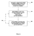
- Figure 3 is a process flow diagram illustrating one embodiment of a method for two step etching method for etching a BARC layer and/or a photoresist layer in a dual damascene structure
- Figures 4A-4B are a sequence of sectional views of a dual damascene fabrication process according to one embodiment of the present invention.
- Embodiments of the present invention include methods for two step etching of a BARC layer in a dual damascene structure.
- the methods preserve the quality of the low-k dielectric film while maintaining a high removal rate by using different gas mixtures at separate BARC layer etching steps in a dual damascene fabrication process.
- the etch process described herein may be performed in any suitable plasma etch chamber.
- One such etch chamber is the ENABLER ® processing chamber, available from Applied Materials, Inc., of Santa Clara, California. It is contemplated that the other etch reactors, including those from other manufacturers, may be adapted to benefit from the invention.
- FIG. 2 depicts a schematic cross-sectional view of one embodiment of a plasma etch system 202 suitable for performing one or more steps of the invention.
- the plasma etch system 202 may include a process chamber body 210 having a conductive chamber wall 230 and a lid 213.
- the temperature of the conductive chamber wall 230 is controlled using liquid-containing conduits (not shown) that are located in and/or around the conductive chamber wall 230.
- the conductive chamber wall 230 is connected to an electrical ground 234.
- a liner 231 is disposed in the process chamber body 210 to cover the interior surfaces of the conductive chamber wall 230.
- the liner 231 serves as a surface protection layer that protects the interior surface of the chamber wall 230 of the process chamber body 210.
- the liner 231 may be fabricated by ceramic materials including Al 2 O 3 , AIN, silicon carbide, Y 2 O 3 , and the like.
- the process chamber body 210 is a vacuum vessel that is coupled through a throttle valve 227 to a vacuum pump 236.
- a support pedestal 216 is disposed in the bottom of the process chamber body 210 to support a substrate 260 positioned thereon during processing.
- the support pedestal 216 may include an electrostatic chuck 226 for retaining the substrate 260.
- a DC power supply 220 is utilized to control the power supplied to the electrostatic chuck 226.
- the support pedestal 216 is coupled to a radio frequency (RF) bias power source 222 through a matching network 224.
- the bias power source 222 is generally capable of producing an RF signal having a tunable frequency of from about 50 kHz to about 60 MHz, and a bias power of about 0 to about 5,000 Watts.
- the bias power source 222 may provide a signal at multiple frequencies, such as about 13.56 MHz and about 2 MHz.
- the bias power source 222 may be a DC or pulsed DC source.
- the temperature of the substrate 260 is at least partially controlled by regulating the temperature of the support pedestal 216.
- the support pedestal 216 includes a cooling plate (not shown) having channels for flowing a coolant.
- a backside gas such as helium (He) gas, provided from a gas source 248, fits provided into channels disposed between the back side of the substrate 260 and grooves (not shown) formed in the surface of the electrostatic chuck 226.
- the backside gas provides efficient heat transfer between the pedestal 216 and the substrate 260.
- the electrostatic chuck 226 may also include a resistive heater (not shown) disposed within the chuck 226 to heat the substrate 260 during processing.
- the substrate 260 is maintained at a temperature of between about 10 to about 500 degrees Celsius.
- a showerhead 232 is mounted to a lid 213 of the process chamber body 210 in a spaced-apart relation to the substrate pedestal 116 facing toward the substrate 260.
- a gas panel 238 is fluidly coupled to a plenum (not shown) defined between the showerhead 232 and the lid 213.
- the showerhead 232 includes a plurality of holes to allow gases provided to the plenum from the gas panel 238 to enter the process chamber body 210.
- the holes in the showerhead 232 may be arranged in different zones such that various gases can be released into the chamber body 210 with different volumetric flow rates.
- the showerhead 232 and/or an upper electrode 228 positioned proximate thereto is coupled to a RF plasma power source 218 through an impedance transformer 219 (e.g., a quarter wavelength matching stub).
- the RF power source 218 is generally capable of producing an RF signal having a tunable frequency of about 50 kHz to about 160 MHz and a source power of about 0 to about 5,000 Watts.
- the RF plasma power source 218 may provide a signal at multiple frequencies, such as about 13.56 MHz or about 2 MHz.
- the plasma etch system 202 may also include one or more coil segments or magnets 212 positioned exterior to the chamber wall 230, near the chamber lid 213. Power to the coil segment(s) 212 is controlled by a DC power source or a low-frequency AC power source 254.
- gas pressure within the interior of the chamber body 210 is controlled using the gas panel 238 and the throttle valve 227. In one embodiment, the gas pressure within the interior of the chamber body 210 is maintained at about 0.1 to about 999 mTorr.
- a controller 240 including a central processing unit (CPU) 244, a memory 242, and support circuits 246, is coupled to the various components of the system 202 to facilitate control of the processes of the present invention.
- the memory 242 can be any computer-readable medium, such as random access memory (RAM), read only memory (ROM), floppy disk, hard disk, or any other form of digital storage, local or remote to the system 202 or CPU 244.
- the support circuits 246 are coupled to the CPU 244 for supporting the CPU 244 in a conventional manner. These circuits include cache, power supplies, clock circuits, input/output circuitry and subsystems, and the like.
- a software routine or a series of program instructions stored in the memory 242, when executed by the CPU 244, causes the plasma etch system 202 to perform an etch process of the present invention.
- Figure 2 only shows one exemplary configuration of various types of plasma etching chambers that can be used to practice the invention.
- different types of source power and bias power can be coupled into the plasma chamber using different coupling mechanisms.
- Using both the source power and the bias power allows independent control of a plasma density and a bias voltage of the substrate with respect to the plasma.
- the source power may not be needed and the plasma is maintained solely by the bias power.
- the plasma density can be enhanced by a magnetic field applied to the vacuum chamber using electromagnets, such as the magnets 212, driven with a low frequency (e.g., 0.1-0.5 Hertz) AC current source or a DC source.
- the plasma may be generated in a different chamber from the one in which the substrate is located, e.g., remote plasma source, and subsequently guided into the chamber using techniques known in the art.
- Figure 3 illustrates a flow diagram of a BARC removal process 300 suitable for use in a dual damascene fabrication process according to one embodiment of the invention.
- Figures 4A-4B are sequential schematic cross-sectional views illustrating different stages of process 300 illustrating the BARC removal process 300.
- the process 300 may be stored in memory 242 as instructions that when executed by the controller 240 cause the process 300 to be performed in the chamber 202.
- the process 300 begins at step 302 by providing a substrate having a film stack suitable for fabricating a dual damascene structure.
- the film stack has been etched to form a dual damascene structure 400 having a trench 422 over a via 420.
- the film stack includes a dielectric bulk insulating layer 410 disposed on a dielectric barrier layer 408 stacked on an underlying dielectric insulating layer 404.
- the dielectric barrier layer 408 not present, the dielectric bulk insulating layer 410 may be directly disposed on the underlying dielectric insulating layer 404.
- the underlying dielectric insulating layer 404 is disposed on a substrate 402 and has at least a conductive layer 406, such as a copper line, embedded therein.
- the dielectric insulating layer 410 is a dielectric material having a dielectric constant less than 4.0, such as less than 3.5.
- suitable materials include carbon-doped silicon oxides (SiOC), such as BLACK DIAMOND ® dielectric material available from Applied Materials, Inc., and other polymers, such as polyamides.
- the dielectric barrier layer 408 is selected from a material having a dielectric constant of about 5.5 or less.
- the dielectric barrier layer 408 is a carbon containing silicon layer (SiC), a nitrogen doped carbon containing silicon layer (SiCN), or the like.
- the dielectric barrier layer 408 may be a BLOK ® dielectric material, available from Applied Materials Inc.
- the trench 422 is formed in the dielectric insulating layer 410 is open through a patterned photoresist layer 412.
- a BARC layer 414 filling in the via 420 is exposed at the bottom of the trench 422.
- the photoresist layer 412 may be conventional carbon-based, organic or polymeric materials used to pattern integrated circuit.
- the BARC 414 may extend from the via 420 to a height beyond a bottom surface 428 of the trench 422, thereby slightly protruding out of the via 420.
- the BARC layer 414 may comprise, for example, organic materials such as polyamides and polysulfide typically having hydrogen and carbon containing elements, or inorganic materials, such as silicon nitride, silicon oxynitride, silicon carbide, and the like.
- the BARC layer 414 is an organic material spun-on the substrate 402.
- the BARC layer 414 may be coated, deposited, or filled in the vias in any other suitable manner.
- the patterned photoresist layer 412 transfers a predetermined pattern and/or feature in the dielectric insulating layer 410.
- the patterned photoresist layer 412 may be consumed or trimmed, leaving a portion of the patterned photoresist layer 412 on the upper surface 416 of the dielectric insulating layer 410.
- the patterned photoresist layer 412 may be substantially removed, thereby exposing the upper surface 416 of the dielectric insulating layer 410.
- a portion of the patterned photoresist layer 412 is remained on the dual damascene structure 400 after predetermined pattern and/or feature are transferred in the dielectric insulating layer 410 to for the trench 422.
- the two step etching process may be performed to remove the BARC layer 414 remained in the vias 420.
- a first etching step is performed to initially etch a portion of the BARC layer 414 filling the via 420 and exposed through the trench 422 by supplying a first gas mixture in the etching chamber 202. If a portion of the patterned photoresist layer 412 may be remained on the substrate surface, the first BARC etching step may also etch the patterned photoresist layer 412.
- the first gas mixture supplied into the etching chamber 202 contains ammonia gas (NH 3 ).
- the first gas mixture is used to remove organic polymers and photoresist crust that may be generated from the previous etching processes and/or present on the substrate surface.
- the hydrogen element in the first gas mixture cleans the organic residues by forming volatile hydrogen carbon compounds which are pumped out of the etching system 202 without damaging the substrate surface.
- the first gas mixture may also passivate the sidewall 426 or exposed surface 428 of the dielectric insulating layer 410, thereby preventing the underlying low-k dielectric substrate from k value shift and dielectric constant increase.
- the first gas mixture may also purge and flush out the residual gas, e.g., fluorine containing gas, from the previous etching process remaining in the etching chamber 202, thereby preventing defect generation or chemical reaction with residual fluorine chemistry which may further attack dielectric insulating layer surface.
- the residual gas e.g., fluorine containing gas
- the BARC layer 414 and/or the patterned photoresist layer 412 is first etched by forming a plasma from the first gas mixture containing NH 3 gas.
- the BARC layer 414 and/or the patterned photoresist layer 412 may be etched in an etch chamber, such as the etching chamber 202 described in Figure 2 , or in other suitable reactors.
- a pressure of the gas mixture in the etch reactor is regulated between about 5 mTorr to about 300 mTorr, and the substrate temperature is maintained between about -10 degrees Celsius and about 55 degrees Celsius.
- RF source power may be applied at a power of about 150 Watts to about 2000 Watts.
- the NH 3 gas may be flowed at a flow rate between about 50 sccm and about 1000 sccm, such as about 100 sccm and about 800 sccm.
- Other inert gas such as N 2 , Ar, He gas, may be flowed and supplied in the first gas mixture at a flow rate between about 50 sccm to about 1000 sccm.
- the first etching step may be terminated by expiration of a predefined time period.
- the first etching step is terminated by processing between about 20 seconds to about 200 seconds.
- the first BARC etching step may be terminated by other suitable method, for example, by monitoring optical emission or by other indicator.
- a second etching step is performed to etch and remove the remaining portion of the BARC layer 414 filling the via 402.
- the second step 306 also removes any patterned photoresist layer 412 remaining on the upper surface 416 of the dielectric insulating layer 410.
- the second etching step is performed using a second gas mixture supplied into the etching chamber 202.
- the second gas mixture includes O 2 gas.
- the second gas mixture containing O 2 gas forms volatile polymers with the residuals and byproducts from the first etching step 304 and reacts with the remaining BARC 414 and photoresist layer 412 on the substrate 402, thereby efficiently removing the residuals, byproducts, remaining BARC 414 and photoresist layer 412 from the substrate 402 out of the etching system 202.
- the oxygen element in the second gas mixture provides a high etching rate and polymer removal rate that not only advantageously promotes removal of the residuals and contaminants but also cleans away the residuals and byproducts that may not be completely removed during the first etching process.
- the BARC layer 414 and/or the photoresist layer 412 is etched by forming a plasma from the second gas mixture containing O 2 .
- the BARC layer and/or the photoresist layer 412 may be etched in an etch system, such as the etch system 202 described in Figure 2 , or in other suitable reactors.
- a pressure of the gas mixture in the etch reactor is regulated between about 5 mTorr to about 50 mTorr, and the substrate temperature is maintained between about -10 degrees Celsius and about 55 degrees Celsius.
- RF source power may be applied at a power of about 150 Watts to about 2000 Watts.
- the O 2 gas may be flowed at a flow rate between about 50 sccm to about 500 sccm.
- the etching time may be processed at between about 20 seconds and about 200 seconds, such as between about 10 seconds to about 60 seconds.
- the second etching step 306 is terminated by expiration of a predefined time period.
- the second BARC etching step may be terminated by processing between about 10 seconds to about 60 seconds.
- the second etching step 306 may also be configured to have a process time substantially equal to the first etching step 304, as described above.
- the process time of the first etching step 304 and the second etching step 306 may be configured to have a time period ratio between about 1:1 to about 4:1.
- the second etching step 306 is terminated by monitoring optical emissions or by other indicator that indicates that the BARC layer 414 and/or the photoresist layer 412 has been completely removed from the substrate 402 or the upper surface 416 of the dielectric insulating layer 410 and a bottom surface 418 in the via 420 has been exposed, as shown in Figure 4B .
- the second gas mixture 306 mainly etches the residuals, byproducts, and the remaining BARC layer 414 and/or the photoresist layer 412 disposed on the substrate without adversely affecting or etching the underlying structures on the substrate, such as the dielectric insulating layer 410. Furthermore, as the second gas mixture provided at the second etching step 306 reacts mainly with the BARC layer 414 and/or the photoresist layer 412, the second etching step 306 advantageously and efficiently removes both organic and/or inorganic materials from the substrate.
- the two step etching process as described at step 304 and step 306 may be repeatedly and consecutively performed on the substrate as indicated by the loop 308 depicted in Figure 3 .
- the two steps etching process described at step 304 and step 306 may be performed in the reverse order.
- the etching step as described at step 306 may be performed first, then followed the etching process as described at step 304.
- the dual damascene structure 400 as depicted in Figure 4 only shows an exemplary embodiment that may be utilized to perform the two step etching process as described in the present invention.
- Other structures such as single damascene structure, via only structure, trench-first structure, and the like, having a BARC layer disposed thereon may also be utilized to perform the two step etching process as described above.
- the method may also be utilized to etch BARC layer found in other substrates.
- the present invention provides a two step etching method for etching a BARC layer with high removal rate and clean efficiency.
- the method advantageously facilitates removal of the BARC layer, photoresist layer, and associated residuals and byproducts from trenches and/or vias in a dual damascene structure without adversely damage underlying dielectric materials disposed on the substrate.
- the two step etching process also provides good sidewall and/or surface protection.
Landscapes
- Internal Circuitry In Semiconductor Integrated Circuit Devices (AREA)
- Drying Of Semiconductors (AREA)
Abstract
Description
- The present invention generally relates to semiconductor processing technologies and, more specifically, to methods for etching a bottom anti-reflective coating (BARC) layer in a dual damascene etching process.
- Integrated circuits have evolved into complex devices that can include millions of components (e.g., transistors, capacitors and resistors) on a single chip. The evolution of chip designs continually requires faster circuitry and greater circuit density. The demands for greater circuit density necessitate a reduction in the dimensions of the integrated circuit components.
- As the dimensions of the integrated circuit components are reduced (e.g. sub-micron dimensions), the materials used to fabricate such components contribute to their electrical performance. For example, metal interconnects with low resistance (e.g., copper and aluminum) provide conductive paths between the components on integrated circuits.
- Copper is particularly advantageous for use in interconnect structures due to its desirable electrical properties. Copper interconnect system are typically fabricated using a damascene process in which trenches and vias are etched into dielectric layers. The trenches and vias are filled with copper which is then planarized using, for example, a chemical-mechanical planarization (CMP) process.
- Copper interconnects are electrically isolated from each other by an insulating material. When the distance between adjacent metal interconnects and/or thickness of the insulating material has sub-micron dimensions, capacitive coupling may potentially occur between such interconnects. Capacitive coupling between adjacent metal interconnects may cause cross talk and/or resistance-capacitance (RC) delay which degrades the overall performance of the integrated circuit. In order to prevent capacitive coupling between adjacent metal interconnects, low dielectric constant (low k) insulating materials (e.g. dielectric constants less than about 4.0) are needed.
-
Figures 1A-1D illustrate an exemplary dual damascene structure formed by a "via-first" processing sequence. Referring first toFigure 1A , a dielectricbulk insulating layer 110 and an underlyingdielectric barrier layer 108 are stacked on another previously formed interconnect having aconductive layer 106 embedded in another dielectricbulk insulating layer 104 disposed on asubstrate 102. An optional polish stop layer or anti-reflective coating (ARC) 112 may be disposed on the dielectricbulk insulating layer 110. The dielectricbulk insulating layer 110 is typically formed from a dielectric material having a dielectric constant lower than 4.0, such as FSG, polymer material, carbon containing silicon layer (SiOC), and the like. - A bottom anti-reflective coating (BARC)
layer 114 is spin-applied to fillvias 128 formed by a via etching process and covers dielectricbulk insulating layer 110 before trench lithography. Aphotoresist layer 116 is disposed on the BARClayer 114 and patterned to define an opening 130 for forming trenches. A BARC etching process is performed to clear away a portion of theBARC layer 114 over the via opening 128 masked by the patternedphotoresist layer 116 before etching the trenches, as shown inFigure 1B . The BARC etching process is performed until the optionalpolish stop layer 112 defined by thephotoresist layer 116 is exposed and theBARC layer 114 filling thevia 128 is etched to a predetermined depth, as shown inFigure 1B . Subsequently, a trench etching process is performed to etch the exposedpolish stop layer 112 and the underlying dielectricbulk insulating layer 110 defined by the patternedphotoresist layer 116, as shown inFigure 1C . The trench etching process etches the dielectricbulk insulating layer 110 into a predetermined depth and definestrenches 122 in the dielectricbulk insulating layer 110. After thetrench 122 has been formed, theremaining BARC layer 114 filling thevia 128 and thephotoresist layer 116 on the top surface of the dielectricbulk insulating layer 110 are removed from thesubstrate 102, thereby forming dual damascene structure on thesubstrate 102, as shown inFigure 1D . - Typically, during the
BARC 114 orphotoresist layer 116 removal process, an oxygen containing plasma etch process is performed to react with theremaining BARC layer 114 and thephotoresist layer 116 on thesubstrate 102, forming a carbon oxide polymer which is pumped out of the processing chamber. However, oxygen present plasma during the removal ofBARC layer 114 andphotoresist layer 116 may attack the exposedsidewall 120 andsurface 126 of thetrenches 122 and/orvias 128 formed in the dielectricbulk insulating layer 110. Oxygen may form a Si-O bond on the surface of the dielectricbulk insulating layer 110, which adversely affect the dielectric properties of the dielectricbulk insulating layer 110. For example, oxygen may accumulate on thesidewall 120 or exposedsurface 126 of the low-k dielectricbulk insulating layer 110, and penetrate into the porous low-k dielectrics, thereby causing the carbon depletion at the film surface. Carbon depletion may cause the dielectric constant of the low-k material to undesirably increase, resulting in a "k loss" of the material dielectric properties. As a result, cross-talk and RC delay may increase after the BARC and photoresist etching process. - Furthermore, removal of the BARC and/or photoresist layer removal process may also leave
contaminants 124, such as residual BARC, residual photoresist layer, impurities, organic or inorganic byproducts in thevias 128 and/ortrenches 122. Thecontaminants 124 present in thevias 128 and/ortrenches 122 may adversely effect the overall integration of the interconnection structure, resulting in poor device reliability and electrical performance. - Therefore, there is a need for an improved process for removing BARC in an interconnection structure.
- Methods for removing a BARC layer from a feature are provided in the present invention. In one embodiment, the method includes providing a substrate having a feature filled with a BARC layer in an etching chamber, supplying a first gas mixture comprising NH3 gas into the chamber to etch a first portion of the BARC layer filling in the feature, and supplying a second gas mixture comprising O2 gas into the etching chamber to etch the remaining portion of the BARC layer disposed in the feature.
- In another embodiment, the method for removing a BARC layer from a feature includes providing a substrate having features formed in a dielectric insulating layer and filled with a BARC layer in an etch chamber, supplying a first gas mixture comprising NH3 into the chamber to etch a portion of the BARC layer filling in the feature, and supplying a second gas mixture comprising O2 gas into the chamber to etch the remaining portion of the BARC layer in the feature.
- In yet another embodiment, the method for removing a BARC layer from a feature includes providing a substrate having features formed in a dielectric insulating layer and filled with a BARC layer in an etch chamber, wherein the dielectric insulating layer has a dielectric constant less than 3.5, supplying a first gas mixture having NH3 gas at between about 50 sccm and about 1000 sccm into the etch chamber to etch a portion of the BARC layer filling in the feature, and supplying a second gas mixture comprising O2 gas at between about 50 sccm and about 500 sccm into the etch chamber to etch the remaining portion of the BARC layer in the feature.
- So that the manner in which the above recited features of the present invention are attained and can be understood in detail, a more particular description of the invention, briefly summarized above, may be had by reference to the embodiments thereof which are illustrated in the appended drawings.
-
Figures 1A-1D are a sequence of sectional views of an exemplary dual damascene fabrication process; -
Figure 2 is a schematic cross-sectional view of a plasma etching chamber used according to one embodiment of the invention; and -
Figure 3 is a process flow diagram illustrating one embodiment of a method for two step etching method for etching a BARC layer and/or a photoresist layer in a dual damascene structure; and -
Figures 4A-4B are a sequence of sectional views of a dual damascene fabrication process according to one embodiment of the present invention. - To facilitate understanding, identical reference numerals have been used, where possible, to designate identical elements that are common to the figures. It is contemplated that elements and features of one embodiment may be beneficially incorporated in other embodiments without further recitation.
- It is to be noted, however, that the appended drawings illustrate only exemplary embodiments of this invention and are therefore not to be considered limiting of its scope, for the invention may admit to other equally effective embodiments.
- Embodiments of the present invention include methods for two step etching of a BARC layer in a dual damascene structure. The methods preserve the quality of the low-k dielectric film while maintaining a high removal rate by using different gas mixtures at separate BARC layer etching steps in a dual damascene fabrication process.
- The etch process described herein may be performed in any suitable plasma etch chamber. One such etch chamber is the ENABLER® processing chamber, available from Applied Materials, Inc., of Santa Clara, California. It is contemplated that the other etch reactors, including those from other manufacturers, may be adapted to benefit from the invention.
-
Figure 2 depicts a schematic cross-sectional view of one embodiment of aplasma etch system 202 suitable for performing one or more steps of the invention. Theplasma etch system 202 may include aprocess chamber body 210 having aconductive chamber wall 230 and alid 213. The temperature of theconductive chamber wall 230 is controlled using liquid-containing conduits (not shown) that are located in and/or around theconductive chamber wall 230. Theconductive chamber wall 230 is connected to anelectrical ground 234. Aliner 231 is disposed in theprocess chamber body 210 to cover the interior surfaces of theconductive chamber wall 230. Theliner 231 serves as a surface protection layer that protects the interior surface of thechamber wall 230 of theprocess chamber body 210. In one embodiment, theliner 231 may be fabricated by ceramic materials including Al2O3, AIN, silicon carbide, Y2O3, and the like. - The
process chamber body 210 is a vacuum vessel that is coupled through athrottle valve 227 to avacuum pump 236. Asupport pedestal 216 is disposed in the bottom of theprocess chamber body 210 to support asubstrate 260 positioned thereon during processing. Thesupport pedestal 216 may include anelectrostatic chuck 226 for retaining thesubstrate 260. ADC power supply 220 is utilized to control the power supplied to theelectrostatic chuck 226. Thesupport pedestal 216 is coupled to a radio frequency (RF) biaspower source 222 through amatching network 224. Thebias power source 222 is generally capable of producing an RF signal having a tunable frequency of from about 50 kHz to about 60 MHz, and a bias power of about 0 to about 5,000 Watts. Thebias power source 222 may provide a signal at multiple frequencies, such as about 13.56 MHz and about 2 MHz. Optionally, thebias power source 222 may be a DC or pulsed DC source. - The temperature of the
substrate 260 is at least partially controlled by regulating the temperature of thesupport pedestal 216. In one embodiment, thesupport pedestal 216 includes a cooling plate (not shown) having channels for flowing a coolant. In addition, a backside gas, such as helium (He) gas, provided from agas source 248, fits provided into channels disposed between the back side of thesubstrate 260 and grooves (not shown) formed in the surface of theelectrostatic chuck 226. The backside gas provides efficient heat transfer between thepedestal 216 and thesubstrate 260. Theelectrostatic chuck 226 may also include a resistive heater (not shown) disposed within thechuck 226 to heat thesubstrate 260 during processing. In one embodiment, thesubstrate 260 is maintained at a temperature of between about 10 to about 500 degrees Celsius. - A
showerhead 232 is mounted to alid 213 of theprocess chamber body 210 in a spaced-apart relation to thesubstrate pedestal 116 facing toward thesubstrate 260. Agas panel 238 is fluidly coupled to a plenum (not shown) defined between theshowerhead 232 and thelid 213. Theshowerhead 232 includes a plurality of holes to allow gases provided to the plenum from thegas panel 238 to enter theprocess chamber body 210. The holes in theshowerhead 232 may be arranged in different zones such that various gases can be released into thechamber body 210 with different volumetric flow rates. - The
showerhead 232 and/or anupper electrode 228 positioned proximate thereto is coupled to a RFplasma power source 218 through an impedance transformer 219 (e.g., a quarter wavelength matching stub). TheRF power source 218 is generally capable of producing an RF signal having a tunable frequency of about 50 kHz to about 160 MHz and a source power of about 0 to about 5,000 Watts. The RFplasma power source 218 may provide a signal at multiple frequencies, such as about 13.56 MHz or about 2 MHz. - The
plasma etch system 202 may also include one or more coil segments ormagnets 212 positioned exterior to thechamber wall 230, near thechamber lid 213. Power to the coil segment(s) 212 is controlled by a DC power source or a low-frequencyAC power source 254. - During substrate processing, gas pressure within the interior of the
chamber body 210 is controlled using thegas panel 238 and thethrottle valve 227. In one embodiment, the gas pressure within the interior of thechamber body 210 is maintained at about 0.1 to about 999 mTorr. - A
controller 240, including a central processing unit (CPU) 244, amemory 242, and supportcircuits 246, is coupled to the various components of thesystem 202 to facilitate control of the processes of the present invention. Thememory 242 can be any computer-readable medium, such as random access memory (RAM), read only memory (ROM), floppy disk, hard disk, or any other form of digital storage, local or remote to thesystem 202 orCPU 244. Thesupport circuits 246 are coupled to theCPU 244 for supporting theCPU 244 in a conventional manner. These circuits include cache, power supplies, clock circuits, input/output circuitry and subsystems, and the like. A software routine or a series of program instructions stored in thememory 242, when executed by theCPU 244, causes theplasma etch system 202 to perform an etch process of the present invention. -
Figure 2 only shows one exemplary configuration of various types of plasma etching chambers that can be used to practice the invention. For example, different types of source power and bias power can be coupled into the plasma chamber using different coupling mechanisms. Using both the source power and the bias power allows independent control of a plasma density and a bias voltage of the substrate with respect to the plasma. In some applications, the source power may not be needed and the plasma is maintained solely by the bias power. The plasma density can be enhanced by a magnetic field applied to the vacuum chamber using electromagnets, such as themagnets 212, driven with a low frequency (e.g., 0.1-0.5 Hertz) AC current source or a DC source. In other applications, the plasma may be generated in a different chamber from the one in which the substrate is located, e.g., remote plasma source, and subsequently guided into the chamber using techniques known in the art. -
Figure 3 illustrates a flow diagram of a BARC removal process 300 suitable for use in a dual damascene fabrication process according to one embodiment of the invention.Figures 4A-4B are sequential schematic cross-sectional views illustrating different stages of process 300 illustrating the BARC removal process 300. The process 300 may be stored inmemory 242 as instructions that when executed by thecontroller 240 cause the process 300 to be performed in thechamber 202. - The process 300 begins at
step 302 by providing a substrate having a film stack suitable for fabricating a dual damascene structure. As shown inFigure 4A , the film stack has been etched to form adual damascene structure 400 having atrench 422 over a via 420. The film stack includes a dielectricbulk insulating layer 410 disposed on adielectric barrier layer 408 stacked on an underlying dielectric insulatinglayer 404. In embodiments thedielectric barrier layer 408 not present, the dielectricbulk insulating layer 410 may be directly disposed on the underlying dielectric insulatinglayer 404. The underlying dielectric insulatinglayer 404 is disposed on asubstrate 402 and has at least aconductive layer 406, such as a copper line, embedded therein. - In one embodiment, the dielectric insulating
layer 410 is a dielectric material having a dielectric constant less than 4.0, such as less than 3.5. Examples of suitable materials include carbon-doped silicon oxides (SiOC), such as BLACK DIAMOND® dielectric material available from Applied Materials, Inc., and other polymers, such as polyamides. Thedielectric barrier layer 408 is selected from a material having a dielectric constant of about 5.5 or less. In one embodiment, thedielectric barrier layer 408 is a carbon containing silicon layer (SiC), a nitrogen doped carbon containing silicon layer (SiCN), or the like. For example, thedielectric barrier layer 408 may be a BLOK® dielectric material, available from Applied Materials Inc. - The
trench 422 is formed in the dielectric insulatinglayer 410 is open through a patternedphotoresist layer 412. ABARC layer 414 filling in the via 420 is exposed at the bottom of thetrench 422. In one embodiment, thephotoresist layer 412 may be conventional carbon-based, organic or polymeric materials used to pattern integrated circuit. TheBARC 414 may extend from the via 420 to a height beyond abottom surface 428 of thetrench 422, thereby slightly protruding out of thevia 420. TheBARC layer 414 may comprise, for example, organic materials such as polyamides and polysulfide typically having hydrogen and carbon containing elements, or inorganic materials, such as silicon nitride, silicon oxynitride, silicon carbide, and the like. In the embodiment depicted inFigure 4A , theBARC layer 414 is an organic material spun-on thesubstrate 402. In another exemplary embodiment, theBARC layer 414 may be coated, deposited, or filled in the vias in any other suitable manner. - The patterned
photoresist layer 412 transfers a predetermined pattern and/or feature in the dielectric insulatinglayer 410. During the process of predetermined pattern and/or feature formation, the patternedphotoresist layer 412 may be consumed or trimmed, leaving a portion of the patternedphotoresist layer 412 on theupper surface 416 of the dielectric insulatinglayer 410. Alternatively, the patternedphotoresist layer 412 may be substantially removed, thereby exposing theupper surface 416 of the dielectric insulatinglayer 410. In embodiments depicted inFigure 4A , a portion of the patternedphotoresist layer 412 is remained on thedual damascene structure 400 after predetermined pattern and/or feature are transferred in the dielectric insulatinglayer 410 to for thetrench 422. In embodiments that thephotoresist layer 412 is not present, the two step etching process may be performed to remove theBARC layer 414 remained in thevias 420. - At
step 304, a first etching step is performed to initially etch a portion of theBARC layer 414 filling the via 420 and exposed through thetrench 422 by supplying a first gas mixture in theetching chamber 202. If a portion of the patternedphotoresist layer 412 may be remained on the substrate surface, the first BARC etching step may also etch the patternedphotoresist layer 412. - In one embodiment, the first gas mixture supplied into the
etching chamber 202 contains ammonia gas (NH3). The first gas mixture is used to remove organic polymers and photoresist crust that may be generated from the previous etching processes and/or present on the substrate surface. The hydrogen element in the first gas mixture cleans the organic residues by forming volatile hydrogen carbon compounds which are pumped out of theetching system 202 without damaging the substrate surface. The first gas mixture may also passivate thesidewall 426 or exposedsurface 428 of the dielectric insulatinglayer 410, thereby preventing the underlying low-k dielectric substrate from k value shift and dielectric constant increase. The first gas mixture may also purge and flush out the residual gas, e.g., fluorine containing gas, from the previous etching process remaining in theetching chamber 202, thereby preventing defect generation or chemical reaction with residual fluorine chemistry which may further attack dielectric insulating layer surface. - In one embodiment, the
BARC layer 414 and/or the patternedphotoresist layer 412 is first etched by forming a plasma from the first gas mixture containing NH3 gas. TheBARC layer 414 and/or the patternedphotoresist layer 412 may be etched in an etch chamber, such as theetching chamber 202 described inFigure 2 , or in other suitable reactors. - Several process parameters are regulated at
step 304 while the first gas mixture is supplied into theetching system 202. In one embodiment, a pressure of the gas mixture in the etch reactor is regulated between about 5 mTorr to about 300 mTorr, and the substrate temperature is maintained between about -10 degrees Celsius and about 55 degrees Celsius. RF source power may be applied at a power of about 150 Watts to about 2000 Watts. The NH3 gas may be flowed at a flow rate between about 50 sccm and about 1000 sccm, such as about 100 sccm and about 800 sccm. Other inert gas, such as N2, Ar, He gas, may be flowed and supplied in the first gas mixture at a flow rate between about 50 sccm to about 1000 sccm. - In one embodiment, the first etching step may be terminated by expiration of a predefined time period. For example, the first etching step is terminated by processing between about 20 seconds to about 200 seconds. In another embodiment, the first BARC etching step may be terminated by other suitable method, for example, by monitoring optical emission or by other indicator.
- At
step 306, a second etching step is performed to etch and remove the remaining portion of theBARC layer 414 filling the via 402. Thesecond step 306 also removes any patternedphotoresist layer 412 remaining on theupper surface 416 of the dielectric insulatinglayer 410. The second etching step is performed using a second gas mixture supplied into theetching chamber 202. In one embodiment, the second gas mixture includes O2 gas. The second gas mixture containing O2 gas forms volatile polymers with the residuals and byproducts from thefirst etching step 304 and reacts with the remainingBARC 414 andphotoresist layer 412 on thesubstrate 402, thereby efficiently removing the residuals, byproducts, remainingBARC 414 andphotoresist layer 412 from thesubstrate 402 out of theetching system 202. The oxygen element in the second gas mixture provides a high etching rate and polymer removal rate that not only advantageously promotes removal of the residuals and contaminants but also cleans away the residuals and byproducts that may not be completely removed during the first etching process. - In one embodiment, the
BARC layer 414 and/or thephotoresist layer 412 is etched by forming a plasma from the second gas mixture containing O2. The BARC layer and/or thephotoresist layer 412 may be etched in an etch system, such as theetch system 202 described inFigure 2 , or in other suitable reactors. - Several process parameters are regulated at
step 306 while the second gas mixture is supplied into thesystem 202. In one embodiment, a pressure of the gas mixture in the etch reactor is regulated between about 5 mTorr to about 50 mTorr, and the substrate temperature is maintained between about -10 degrees Celsius and about 55 degrees Celsius. RF source power may be applied at a power of about 150 Watts to about 2000 Watts. The O2 gas may be flowed at a flow rate between about 50 sccm to about 500 sccm. The etching time may be processed at between about 20 seconds and about 200 seconds, such as between about 10 seconds to about 60 seconds. - The
second etching step 306 is terminated by expiration of a predefined time period. For example, the second BARC etching step may be terminated by processing between about 10 seconds to about 60 seconds. In one embodiment, thesecond etching step 306 may also be configured to have a process time substantially equal to thefirst etching step 304, as described above. Alternatively, the process time of thefirst etching step 304 and thesecond etching step 306 may be configured to have a time period ratio between about 1:1 to about 4:1. In another embodiment, thesecond etching step 306 is terminated by monitoring optical emissions or by other indicator that indicates that theBARC layer 414 and/or thephotoresist layer 412 has been completely removed from thesubstrate 402 or theupper surface 416 of the dielectric insulatinglayer 410 and abottom surface 418 in the via 420 has been exposed, as shown inFigure 4B . - Since the sidewall and surface of the dielectric insulating
layer 410 are passivated and protected by the polymer formed from exposure to the first gas mixture atstep 304, thesecond gas mixture 306 mainly etches the residuals, byproducts, and the remainingBARC layer 414 and/or thephotoresist layer 412 disposed on the substrate without adversely affecting or etching the underlying structures on the substrate, such as the dielectric insulatinglayer 410. Furthermore, as the second gas mixture provided at thesecond etching step 306 reacts mainly with theBARC layer 414 and/or thephotoresist layer 412, thesecond etching step 306 advantageously and efficiently removes both organic and/or inorganic materials from the substrate. - The two step etching process as described at
step 304 and step 306 may be repeatedly and consecutively performed on the substrate as indicated by theloop 308 depicted inFigure 3 . Alternatively, the two steps etching process described atstep 304 and step 306 may be performed in the reverse order. For example, the etching step as described atstep 306 may be performed first, then followed the etching process as described atstep 304. - The
dual damascene structure 400 as depicted inFigure 4 only shows an exemplary embodiment that may be utilized to perform the two step etching process as described in the present invention. Other structures, such as single damascene structure, via only structure, trench-first structure, and the like, having a BARC layer disposed thereon may also be utilized to perform the two step etching process as described above. The method may also be utilized to etch BARC layer found in other substrates. - Thus, the present invention provides a two step etching method for etching a BARC layer with high removal rate and clean efficiency. The method advantageously facilitates removal of the BARC layer, photoresist layer, and associated residuals and byproducts from trenches and/or vias in a dual damascene structure without adversely damage underlying dielectric materials disposed on the substrate. The two step etching process also provides good sidewall and/or surface protection.
- While the foregoing is directed to embodiments of the present invention, other and further embodiments of the invention may be devised without departing from the basic scope thereof, and the scope thereof is determined by the claims that follow.
Claims (22)
- A method for removing a BARC layer from a feature, comprising:providing a substrate having a feature filled with a BARC layer in an etching chamber;supplying a first gas mixture comprising NH3 gas into the chamber to etch a first portion of the BARC layer filling in the feature; andsupplying a second gas mixture comprising O2 gas into the etching chamber to etch the remaining portion of the BARC layer disposed in the feature.
- The method of claim 1, wherein the step of supplying the first gas mixture further comprises:flowing NH3 into the etching chamber having at a flow rate between 50 sccm and 1000 sccm.
- The method of claim 1, wherein the step of supplying the first gas mixture further comprises:maintaining a process pressure at between about 5 mTorr to about 300 mTorr.
- The method of claim 1, wherein the step of supplying the first gas mixture further comprises:controlling substrate temperature between about -10 degrees Celsius to about 55 degrees Celsius.
- The method of claim 1, wherein the step of supplying the first gas mixture further comprises:applying a plasma power at between about 150 Watts to about 2000 Watts.
- The method of claim 1, wherein the step of supplying the first gas mixture further comprises:etching the first portion of the BARC layer filling in the features at a process time between about 20 seconds and about 200 seconds.
- The method of claim 1, wherein the step of supplying the second gas mixture further comprises:flowing O2 gas into the etching chamber at a flow rate between 50 sccm and 500 sccm.
- The method of claim 1, wherein the step of supplying the second gas mixture further comprises:maintaining a process pressure at between about 5 mTorr to about 50 mTorr.
- The method of claim 1, wherein the step of supplying the second gas mixture further comprises:controlling substrate temperature between about -10 degrees Celsius to about 55 degrees Celsius.
- The method of claim 1, wherein the step of supplying the second gas mixture further comprises:applying a plasma power at between about 150 Watts to about 2000 Watts.
- The method of claim 1, wherein the step of supplying the second gas mixture further comprises:etching the remaining portion of the BARC layer filling in the features at a process time between about 10 seconds and about 60 seconds.
- The method of claim 1, wherein the etching time between the first gas mixture supply and the second gas mixture supply has a ratio between about 1:1 and about 4:1.
- The method of claim 1, wherein the damascene structure includes a dielectric insulating layer having a dielectric constant less than 3.5.
- The method of claim 1, wherein the damascene structure includes a dielectric insulating layer comprising carbon doped silicon oxide.
- The method of claim 1, wherein the step of providing further comprises:providing the substrate having a photoresist layer disposed on an upper surface of the substrate.
- The method of claim 15, wherein the first gas mixture and the second gas mixture supplied into the etching chamber etch the photoresist layer while etching the BARC layer.
- A method for removing a BARC layer from a feature, comprising:providing a substrate having a feature formed in a dielectric insulating layer and filled with a BARC layer in an etch chamber;supplying a first gas mixture comprising NH3 into the chamber to etch a portion of the BARC layer filling in the feature; andsupplying a second gas mixture comprising O2 gas into the chamber to etch the remaining portion of the BARC layer in the feature.
- The method of claim 17, wherein the step of supplying the first gas mixture further comprising:flowing the NH3 gas at a rate between about 50 sccm to about 1000 sccm.
- The method of claim 17, wherein the step of supplying the second gas mixture further comprising:flowing the O2 gas at a rate between about 50 sccm to about 500 sccm.
- The method of claim 17, wherein the etching time between the first gas mixture supply and the second gas mixture supply has a ratio between about 1:1 and about 4:1.
- The method of claim 17, wherein the dielectric insulating layer has a dielectric constant less than 3.5.
- A method for removing a BARC layer from a feature, comprising:providing a substrate having a feature formed in a dielectric insulating layer and filled with a BARC layer in an etch chamber, wherein the dielectric insulating layer has a dielectric constant less than 3.5;supplying a first gas mixture having NH3 gas at between about 50 sccm and about 1000 sccm into the etch chamber to etch a portion of the BARC layer filling in the feature; andsupplying a second gas mixture comprising O2 gas at between about 50 sccm and about 500 sccm into the etch chamber to etch the remaining portion of the BARC layer in the feature.
Applications Claiming Priority (1)
| Application Number | Priority Date | Filing Date | Title |
|---|---|---|---|
| US11/608,611 US7718543B2 (en) | 2006-12-08 | 2006-12-08 | Two step etching of a bottom anti-reflective coating layer in dual damascene application |
Publications (2)
| Publication Number | Publication Date |
|---|---|
| EP1930939A2 true EP1930939A2 (en) | 2008-06-11 |
| EP1930939A3 EP1930939A3 (en) | 2009-09-09 |
Family
ID=39156397
Family Applications (1)
| Application Number | Title | Priority Date | Filing Date |
|---|---|---|---|
| EP07122597A Withdrawn EP1930939A3 (en) | 2006-12-08 | 2007-12-07 | Two step etching of a bottom anti-reflective coating layer in dual damascene application |
Country Status (7)
| Country | Link |
|---|---|
| US (1) | US7718543B2 (en) |
| EP (1) | EP1930939A3 (en) |
| JP (1) | JP5232455B2 (en) |
| KR (1) | KR100917291B1 (en) |
| CN (1) | CN100552891C (en) |
| SG (1) | SG143239A1 (en) |
| TW (1) | TWI356454B (en) |
Families Citing this family (8)
| Publication number | Priority date | Publication date | Assignee | Title |
|---|---|---|---|---|
| CN101989575B (en) * | 2009-08-06 | 2012-10-31 | 中芯国际集成电路制造(上海)有限公司 | Polishing method of dielectric layer of complementary metal-oxide-semiconductor transistor (CMOS) image sensor |
| US8518832B1 (en) | 2011-06-27 | 2013-08-27 | Western Digital (Fremont), Llc | Process for masking and removal of residue from complex shapes |
| US8703397B1 (en) | 2012-03-29 | 2014-04-22 | Western Digital (Fremont), Llc | Method for providing side shields for a magnetic recording transducer |
| US9437449B2 (en) * | 2012-12-31 | 2016-09-06 | Texas Instruments Incorporated | Uniform, damage free nitride etch |
| US9460934B2 (en) | 2013-03-15 | 2016-10-04 | Globalfoundries Inc. | Wet strip process for an antireflective coating layer |
| CN104124202A (en) * | 2013-04-28 | 2014-10-29 | 中芯国际集成电路制造(上海)有限公司 | Formation method of dual damascene structure |
| US9001467B1 (en) | 2014-03-05 | 2015-04-07 | Western Digital (Fremont), Llc | Method for fabricating side shields in a magnetic writer |
| TWI768718B (en) * | 2020-04-28 | 2022-06-21 | 台灣積體電路製造股份有限公司 | Methods of manufacturing semiconductor device |
Family Cites Families (28)
| Publication number | Priority date | Publication date | Assignee | Title |
|---|---|---|---|---|
| US5950126A (en) * | 1996-12-03 | 1999-09-07 | Nokia Telecommunications Oy | Network operator controlled usage of long distance carriers |
| US6635185B2 (en) * | 1997-12-31 | 2003-10-21 | Alliedsignal Inc. | Method of etching and cleaning using fluorinated carbonyl compounds |
| US6140226A (en) * | 1998-01-16 | 2000-10-31 | International Business Machines Corporation | Dual damascene processing for semiconductor chip interconnects |
| US6147009A (en) * | 1998-06-29 | 2000-11-14 | International Business Machines Corporation | Hydrogenated oxidized silicon carbon material |
| US6544882B1 (en) * | 2000-01-13 | 2003-04-08 | Taiwan Semiconductor Manufacturing Company | Method to improve reliability of multilayer structures of FSG (F-doped SiO2) dielectric layers and aluminum-copper-TiN layers in integrated circuits |
| JP3803528B2 (en) | 2000-03-31 | 2006-08-02 | 株式会社東芝 | Semiconductor device manufacturing method and semiconductor device |
| US6514850B2 (en) * | 2001-01-31 | 2003-02-04 | Applied Materials, Inc. | Interface with dielectric layer and method of making |
| US20020139771A1 (en) * | 2001-02-22 | 2002-10-03 | Ping Jiang | Gas switching during an etch process to modulate the characteristics of the etch |
| US20020187627A1 (en) * | 2001-06-06 | 2002-12-12 | Yu-Shen Yuang | Method of fabricating a dual damascene structure |
| JP5038567B2 (en) * | 2001-09-26 | 2012-10-03 | 東京エレクトロン株式会社 | Etching method |
| US6759327B2 (en) * | 2001-10-09 | 2004-07-06 | Applied Materials Inc. | Method of depositing low k barrier layers |
| US6652712B2 (en) * | 2001-12-19 | 2003-11-25 | Applied Materials, Inc | Inductive antenna for a plasma reactor producing reduced fluorine dissociation |
| US20030228768A1 (en) * | 2002-06-05 | 2003-12-11 | Applied Materials, Inc. | Dielectric etching with reduced striation |
| US6903023B2 (en) * | 2002-09-16 | 2005-06-07 | International Business Machines Corporation | In-situ plasma etch for TERA hard mask materials |
| US7071112B2 (en) * | 2002-10-21 | 2006-07-04 | Applied Materials, Inc. | BARC shaping for improved fabrication of dual damascene integrated circuit features |
| JP4594235B2 (en) * | 2002-12-23 | 2010-12-08 | 東京エレクトロン株式会社 | Method for etching an ARC layer |
| US7132369B2 (en) * | 2002-12-31 | 2006-11-07 | Applied Materials, Inc. | Method of forming a low-K dual damascene interconnect structure |
| US6705886B1 (en) | 2003-01-23 | 2004-03-16 | Fci Americas Technology, Inc. | Electrical connector having connector position assurance member |
| US6780782B1 (en) * | 2003-02-04 | 2004-08-24 | Taiwan Semiconductor Manufacturing Company, Ltd. | Bi-level resist structure and fabrication method for contact holes on semiconductor substrates |
| US6923796B2 (en) * | 2003-02-25 | 2005-08-02 | The Procter & Gamble Company | Dimensionally optimized menstrual fluid management device |
| US6921727B2 (en) * | 2003-03-11 | 2005-07-26 | Applied Materials, Inc. | Method for modifying dielectric characteristics of dielectric layers |
| US7309448B2 (en) * | 2003-08-08 | 2007-12-18 | Applied Materials, Inc. | Selective etch process of a sacrificial light absorbing material (SLAM) over a dielectric material |
| US6972253B2 (en) * | 2003-09-09 | 2005-12-06 | Taiwan Semiconductor Manufacturing Company, Ltd. | Method for forming dielectric barrier layer in damascene structure |
| US20050059234A1 (en) * | 2003-09-16 | 2005-03-17 | Applied Materials, Inc. | Method of fabricating a dual damascene interconnect structure |
| KR20070009729A (en) | 2004-05-11 | 2007-01-18 | 어플라이드 머티어리얼스, 인코포레이티드 | Carbon-doped-Si oxide etch using H2 addition in carbon fluoride etching chemistry |
| US7508747B2 (en) * | 2004-05-24 | 2009-03-24 | Hewlett-Packard Development Company, L.P. | Derivative qualified zero crossing detector apparatus and methods |
| JP2005353633A (en) * | 2004-06-08 | 2005-12-22 | Sony Corp | Semiconductor device manufacturing method and semiconductor device |
| US7253353B2 (en) * | 2004-06-30 | 2007-08-07 | General Motors Corporation | Thermoelectric augmented hybrid electric propulsion system |
-
2006
- 2006-12-08 US US11/608,611 patent/US7718543B2/en not_active Expired - Fee Related
-
2007
- 2007-12-07 SG SG200718443-5A patent/SG143239A1/en unknown
- 2007-12-07 EP EP07122597A patent/EP1930939A3/en not_active Withdrawn
- 2007-12-07 JP JP2007316730A patent/JP5232455B2/en not_active Expired - Fee Related
- 2007-12-10 KR KR1020070127403A patent/KR100917291B1/en not_active Expired - Fee Related
- 2007-12-10 CN CNB2007101987203A patent/CN100552891C/en not_active Expired - Fee Related
- 2007-12-10 TW TW096147116A patent/TWI356454B/en not_active IP Right Cessation
Also Published As
| Publication number | Publication date |
|---|---|
| SG143239A1 (en) | 2008-06-27 |
| TWI356454B (en) | 2012-01-11 |
| CN101197277A (en) | 2008-06-11 |
| US20080138997A1 (en) | 2008-06-12 |
| JP5232455B2 (en) | 2013-07-10 |
| US7718543B2 (en) | 2010-05-18 |
| CN100552891C (en) | 2009-10-21 |
| KR100917291B1 (en) | 2009-09-11 |
| JP2008147668A (en) | 2008-06-26 |
| KR20080053239A (en) | 2008-06-12 |
| EP1930939A3 (en) | 2009-09-09 |
| TW200834715A (en) | 2008-08-16 |
Similar Documents
| Publication | Publication Date | Title |
|---|---|---|
| US7977245B2 (en) | Methods for etching a dielectric barrier layer with high selectivity | |
| US7618889B2 (en) | Dual damascene fabrication with low k materials | |
| US7115517B2 (en) | Method of fabricating a dual damascene interconnect structure | |
| US7132369B2 (en) | Method of forming a low-K dual damascene interconnect structure | |
| EP2001814A2 (en) | Methods for etching a bottom anti-reflective coating layer in dual damascene application | |
| EP1930939A2 (en) | Two step etching of a bottom anti-reflective coating layer in dual damascene application | |
| JP2002525840A (en) | In situ integrated oxide etching process especially useful for copper dual damascene | |
| WO2000003432A1 (en) | Plasma etch process of a dielectric multilayer structure particularly useful for dual damascene | |
| WO2006055460A2 (en) | Post-etch treatment to remove residues | |
| US20070026665A1 (en) | Method of fabricating a dual damascene interconnect structure | |
| JP2005268312A (en) | Resist removing method and semiconductor device manufactured using the same | |
| US7572734B2 (en) | Etch depth control for dual damascene fabrication process | |
| JP2005005697A (en) | Manufacturing method of semiconductor device | |
| US7393795B2 (en) | Methods for post-etch deposition of a dielectric film | |
| US20090117745A1 (en) | Methods for selectively etching a barrier layer in dual damascene applications | |
| US20050287796A1 (en) | Methods of fabricating metal lines in semiconductor devices |
Legal Events
| Date | Code | Title | Description |
|---|---|---|---|
| PUAI | Public reference made under article 153(3) epc to a published international application that has entered the european phase |
Free format text: ORIGINAL CODE: 0009012 |
|
| AK | Designated contracting states |
Kind code of ref document: A2 Designated state(s): AT BE BG CH CY CZ DE DK EE ES FI FR GB GR HU IE IS IT LI LT LU LV MC MT NL PL PT RO SE SI SK TR |
|
| AX | Request for extension of the european patent |
Extension state: AL BA HR MK RS |
|
| PUAL | Search report despatched |
Free format text: ORIGINAL CODE: 0009013 |
|
| AK | Designated contracting states |
Kind code of ref document: A3 Designated state(s): AT BE BG CH CY CZ DE DK EE ES FI FR GB GR HU IE IS IT LI LT LU LV MC MT NL PL PT RO SE SI SK TR |
|
| AX | Request for extension of the european patent |
Extension state: AL BA HR MK RS |
|
| AKX | Designation fees paid | ||
| STAA | Information on the status of an ep patent application or granted ep patent |
Free format text: STATUS: THE APPLICATION IS DEEMED TO BE WITHDRAWN |
|
| 18D | Application deemed to be withdrawn |
Effective date: 20100310 |
|
| REG | Reference to a national code |
Ref country code: DE Ref legal event code: 8566 |