EP1930766A1 - Abberation correction apparatus - Google Patents
Abberation correction apparatus Download PDFInfo
- Publication number
- EP1930766A1 EP1930766A1 EP07023158A EP07023158A EP1930766A1 EP 1930766 A1 EP1930766 A1 EP 1930766A1 EP 07023158 A EP07023158 A EP 07023158A EP 07023158 A EP07023158 A EP 07023158A EP 1930766 A1 EP1930766 A1 EP 1930766A1
- Authority
- EP
- European Patent Office
- Prior art keywords
- liquid crystal
- electrode layer
- light beam
- aberration
- crystal device
- Prior art date
- Legal status (The legal status is an assumption and is not a legal conclusion. Google has not performed a legal analysis and makes no representation as to the accuracy of the status listed.)
- Ceased
Links
- 239000004973 liquid crystal related substance Substances 0.000 claims abstract description 68
- 230000004075 alteration Effects 0.000 claims abstract description 40
- 230000001747 exhibiting effect Effects 0.000 claims abstract description 3
- 239000010410 layer Substances 0.000 description 44
- 230000003287 optical effect Effects 0.000 description 29
- 230000035945 sensitivity Effects 0.000 description 15
- 238000010586 diagram Methods 0.000 description 6
- 238000000034 method Methods 0.000 description 5
- 239000011521 glass Substances 0.000 description 3
- 230000000052 comparative effect Effects 0.000 description 2
- 238000001514 detection method Methods 0.000 description 2
- 239000004065 semiconductor Substances 0.000 description 2
- 230000005494 condensation Effects 0.000 description 1
- 238000009833 condensation Methods 0.000 description 1
- 230000010485 coping Effects 0.000 description 1
- 230000002349 favourable effect Effects 0.000 description 1
- 239000011241 protective layer Substances 0.000 description 1
- 238000011160 research Methods 0.000 description 1
Images


Classifications
-
- G—PHYSICS
- G02—OPTICS
- G02F—OPTICAL DEVICES OR ARRANGEMENTS FOR THE CONTROL OF LIGHT BY MODIFICATION OF THE OPTICAL PROPERTIES OF THE MEDIA OF THE ELEMENTS INVOLVED THEREIN; NON-LINEAR OPTICS; FREQUENCY-CHANGING OF LIGHT; OPTICAL LOGIC ELEMENTS; OPTICAL ANALOGUE/DIGITAL CONVERTERS
- G02F1/00—Devices or arrangements for the control of the intensity, colour, phase, polarisation or direction of light arriving from an independent light source, e.g. switching, gating or modulating; Non-linear optics
- G02F1/01—Devices or arrangements for the control of the intensity, colour, phase, polarisation or direction of light arriving from an independent light source, e.g. switching, gating or modulating; Non-linear optics for the control of the intensity, phase, polarisation or colour
- G02F1/13—Devices or arrangements for the control of the intensity, colour, phase, polarisation or direction of light arriving from an independent light source, e.g. switching, gating or modulating; Non-linear optics for the control of the intensity, phase, polarisation or colour based on liquid crystals, e.g. single liquid crystal display cells
- G02F1/133—Constructional arrangements; Operation of liquid crystal cells; Circuit arrangements
- G02F1/1333—Constructional arrangements; Manufacturing methods
- G02F1/1343—Electrodes
- G02F1/134309—Electrodes characterised by their geometrical arrangement
-
- G—PHYSICS
- G02—OPTICS
- G02F—OPTICAL DEVICES OR ARRANGEMENTS FOR THE CONTROL OF LIGHT BY MODIFICATION OF THE OPTICAL PROPERTIES OF THE MEDIA OF THE ELEMENTS INVOLVED THEREIN; NON-LINEAR OPTICS; FREQUENCY-CHANGING OF LIGHT; OPTICAL LOGIC ELEMENTS; OPTICAL ANALOGUE/DIGITAL CONVERTERS
- G02F2203/00—Function characteristic
- G02F2203/18—Function characteristic adaptive optics, e.g. wavefront correction
Definitions
- the liquid crystal device of the above type has the problem that, unless the potentials which are impressed on the respective divided regions formed in the electrode layers are appropriately controlled, the aberration correction cannot be made at a high precision.
- a fine solid line in Fig. 4C indicates every region, the phase change magnitude which corresponds to a potential difference from a reference potential belonging to the high sensitivity region, as regards the potential which belongs to the high sensitivity region and which is impressed on the regions formed in the first electrode layer 13.
- a fine dotted line in Fig. 4C indicates every region, the phase change magnitude which corresponds to a potential difference from the reference potential, as regards the potential which belongs to the high sensitivity region and which is impressed on the regions formed in the second electrode layer 14.
- a bold solid line in Fig. 4C indicates an aberration which appears before the correction based on the liquid crystal device 8.
Landscapes
- Physics & Mathematics (AREA)
- Nonlinear Science (AREA)
- Geometry (AREA)
- Mathematical Physics (AREA)
- Chemical & Material Sciences (AREA)
- Crystallography & Structural Chemistry (AREA)
- General Physics & Mathematics (AREA)
- Optics & Photonics (AREA)
- Liquid Crystal (AREA)
- Optical Head (AREA)
Abstract
Description
- The present invention relates to an aberration correction apparatus.
- At present, optical disks such as CDs and DVDs have spread and have come into general use. In addition, researches on the higher density of the optical disk have been made, and an optical disk heightened in density, such as Blu-ray Disk (hereinbelow, abbreviated to "BD"), has also been put into practical use.
- In this regard, an optical pickup apparatus which plays back and records information for a plurality of sorts of optical disks with a single objective lens has been developed as an optical pickup which is installed in an optical disk apparatus. In case of coping with the plurality of sorts of optical disks with the single objective lens, even when the objective lens has been adjusted so that any aberration may not appear as to the optical disk of one sort by way of example, an aberration sometimes appears in the playback etc. of the information as to the optical disk of the other sort. Therefore, it is common to employ a configuration wherein a liquid crystal device is arranged in the optical pickup apparatus, and wherein a voltage is applied to the liquid crystal device so as to correct the aberration. In addition, regarding the liquid crystal device which is arranged for such a purpose, a type wherein regions divided concentrically are formed in both of two electrode layers included in the liquid crystal device and wherein potentials to be impressed on the respective divided regions are controlled, thereby to correct the aberration, has been introduced in large numbers in
JP-A-2001-273663 - The liquid crystal device of the above type, however, has the problem that, unless the potentials which are impressed on the respective divided regions formed in the electrode layers are appropriately controlled, the aberration correction cannot be made at a high precision.
- The present invention has for its object to provide, in an aberration correction apparatus which includes a liquid crystal device that has two electrode layers each being formed with regions divided concentrically, an aberration correction apparatus which permits the correction of an aberration at a high precision.
- In order to accomplish the object, an aberration correction apparatus according to the invention consists in an aberration correction apparatus comprising:
- a liquid crystal device which includes a first electrode layer that is formed with regions divided concentrically, a second electrode layer that is formed with regions divided concentrically, and a liquid crystal that is sandwiched in between the first electrode layer and the second electrode layer, and which transmits an incident light beam therethrough;
- an objective lens which condenses the light beam transmitted through the liquid crystal device; and
- a liquid-crystal-device drive circuit which drives the liquid crystal device; characterized in:
- that the liquid-crystal-device drive circuit impresses a potential which belongs to a predetermined region included in a liquid crystal characteristic that is a relationship between potentials impressed on the respective electrode layers sandwiching in the liquid crystal therebetween and a phase change magnitude of the light beam transmitted through the liquid crystal, on the concentric regions formed in the first electrode layer, and that it impresses a potential which belongs to a region included in the liquid crystal characteristic and exhibiting a smaller phase change magnitude per unit drive voltage than in the predetermined region, on the concentric regions formed in the second electrode layer, whereby an aberration of the light beam is corrected.
- According to such a configuration, the phase change magnitude of the light beam which is transmitted through the liquid crystal device can be brought near to an aberration which appears before the correction, as far as possible, and the aberration can be corrected at a high precision.
- Besides, in the above configuration, the number of the concentric regions which are formed in the second electrode layer should desirably be made larger than the number of the concentric regions which are formed in the first electrode layer. According to such a configuration, the potential which is set for the second electrode layer can be set more finely, and the aberration can be corrected at a higher precision.
-
-
Fig. 1 is a schematic diagram showing the optical system of an optical pickup according to the present invention; -
Fig. 2 is a schematic perspective view showing the structure of a liquid crystal device; -
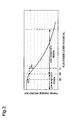
Fig. 3 is a graph showing a liquid crystal characteristic; -
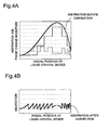
Fig. 4A is a diagram showing a method for driving the liquid crystal device according to the invention; -
Fig. 4B is a diagram showing an aberration correction result based on the method for driving the liquid crystal device according to the invention; -
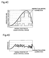
Fig. 4C is a diagram showing a method for driving the liquid crystal device as is a comparative example to the invention; and -
Fig. 4D is a diagram showing an aberration correction result based on the method for driving the liquid crystal device as is the comparative example to the invention. - Now, embodiments of the present invention will be described with reference to the drawings.
-
Fig. 1 is a schematic diagram showing the optical system of anoptical pickup 1 according to the invention as is installed in an optical disk apparatus. Theoptical pickup 1 includes a first light source 2, asecond light source 3, adichroic prism 4, acollimate lens 5, a beam splitter 6, astartup mirror 7, a liquid crystal device 8, an objective lens 9, adetection lens 10 and aphotodetector 11. - The first light source 2 is a semiconductor laser which can emit a light beam of 650 nm band corresponding to a DVD, while the
second light source 3 is a semiconductor laser which can emit a light beam of 405 nm band corresponding to a BD. - The
dichroic prism 4 transmits therethrough the light beam which is emitted from the first light source 2 for emitting the light beam for the DVD, and it reflects therefrom the light beam which is emitted from thesecond light source 3 for emitting the light beam for the BD. In addition, thedichroic prism 4 brings the optic axes of the light beams emitted from the first light source 2 and thesecond light source 3, into agreement. The light beam transmitted through or reflected from thedichroic mirror 4 is conveyed to thecollimate lens 5. - The
collimate lens 5 converts the light beam having passed through thedichroic prism 4, into parallel light. Here, the expression "parallel light" signifies light in which all the optical paths of the light beam emitted from the first light source 2 or thesecond light source 3 are substantially parallel to the optic axis. The light beam converted into the parallel light by thecollimate lens 5 is conveyed to the beam splitter 6. - The beam splitter 6 transmits therethrough the light beam conveyed from the
collimate lens 5, so as to guide the transmitted light beam onto the side of anoptical disk 12, and it reflects reflection light from theoptical disk 12, so as to guide the reflected light onto the side of thephotodetector 11. The light beam transmitted through the beam splitter 6 is conveyed to thestartup mirror 7. - The
startup mirror 7 reflects the light beam transmitted through the beam splitter 6, and guides the reflected light beam toward theoptical disk 12. The light beam reflected from thestartup mirror 7 is conveyed to the liquid crystal device 8. - The liquid crystal device 8 is a device which permits the control of the phase of the light beam that is transmitted through this liquid crystal device 8, by utilizing the property that, when a voltage is applied to a liquid crystal sandwiched in between electrode layers, the molecules of the liquid crystal change their orientation direction. Owing to the arrangement of the liquid crystal device 8, it becomes possible to correct an aberration which occurs due to the difference of the thickness of a protective layer for protecting the
record surface 12a of theoptical disk 12, and so forth. In this embodiment, the correction of the aberration is possible as to the light beam which is emitted from the light source for the DVD (the first light source 2). Incidentally, the details of the liquid crystal device 8 will be stated later. The light beam having passed through the liquid crystal device 8 is conveyed to the objective lens 9. - The objective lens 9 condenses the light beam transmitted through the liquid crystal device 8, onto the
record surface 12a of theoptical disk 12. The objective lens 9 in this embodiment is designed so as not to give rise to any aberration, as to the light beam which is emitted from the light source for the BD (the second light source 3). In this case, the light beam, which is emitted from the light source for the DVD (the first light source 2) and which is then transmitted through the objective lens 9, undergoes the aberration. Therefore, the liquid crystal device 8 is arranged in the optical system of theoptical pickup 1, whereby the aberration can be corrected. Besides, the objective lens 9 is made movable in, for example, up and down directions and right and left directions inFig. 1 , by an objective lens actuator not shown, whereby the position thereof is controlled on the basis of a focus servo signal and a tracking servo signal. Besides, the liquid crystal device 8 is also mounted on the objective lens actuator so as to be movable with the objective lens 9. - The reflection light reflected from the
optical disk 12 is passed through the objective lens 9 and the liquid crystal device 8 in this order, and is reflected from thestartup mirror 7. Thereafter, the reflection light is further reflected from the beam splitter 6, and it is condensed onto a light receiving portion provided in thephotodetector 11, by thedetection lens 10. - The
photodetector 11 converts received light information into an electric signal and outputs the electric signal to, for example, an RF amplifier not shown, thereby to generate the playback signal of data recorded on therecord surface 12a, and the focus servo signal and the tracking servo signal. - Here,
Fig. 2 shows a schematic perspective view illustrating the structure of the liquid crystal device 8. The liquid crystal device 8 includes a liquid crystal 15, a first electrode layer 13 and a second electrode layer 14 between which the liquid crystal 15 is sandwiched in, and twoglass plates 16 between which a portion configured of the liquid crystal 15, the first electrode layer 13 and the second electrode layer 14 is sandwiched in. Each of the first electrode layer 13 and the second electrode layer 14 is formed with regions divided concentrically, and the number of the regions formed in the second electrode layer 14 is larger than the number of the regions formed in the first electrode layer 13. - Besides, the individual regions formed in the first electrode layer 13 and the second electrode layer 14 are electrically connected with a liquid-crystal-device drive circuit not shown. The liquid-crystal-device drive circuit may be disposed in the
optical pickup 1, or may well be disposed in the optical disk apparatus outside theoptical pickup 1. The light beam reflected from thestartup mirror 7 is transmitted through theglass plate 16, the first electrode layer 13, the liquid crystal 15, the second electrode layer 14 and theglass plate 16 in the order mentioned, whereupon it enters the objective lens 9. - Next, a method for driving the liquid crystal device 8 will be described.
-
Fig. 3 shows a liquid crystal characteristic which is the relationship between potentials that are impressed on the respective electrode layers sandwiching in the liquid crystal therebetween and the phase change magnitude of the light beam that is transmitted through the liquid crystal. In a case where the potential of a certain point on the axis of abscissas inFig. 3 is impressed on one of the two electrodes and where the potential of another point on the axis of abscissas inFig. 3 is impressed on the other electrode, the phase of the light beam which is transmitted through the liquid crystal is changed by the phase change magnitude which corresponds to the distance in the direction of the axis of ordinates between individual points on a curve inFig. 3 as correspond to the respective potentials. - The liquid crystal characteristic has a high sensitivity region being a region in which the phase change magnitude per unit drive voltage is large, and a low sensitivity region being a region in which the phase change magnitude per unit drive voltage is smaller than in the high sensitivity region. In the invention, the potential which belongs to the high sensitivity region is impressed on the regions formed in the first electrode layer 13 included in the liquid crystal device 8 by the liquid-crystal-device drive circuit, whereas the potential which belongs to the low sensitivity region is impressed on the regions formed in the second electrode layer 14 included in the liquid crystal device 8 by the liquid-crystal-device drive circuit.
- A fine solid line in
Fig. 4A indicates every region, the phase change magnitude (P1 inFig. 3 ) which corresponds to a potential difference from a reference potential (E0 inFig. 3 ) at the boundary between the high sensitivity region and the low sensitivity region, as regards the potential (E1 inFig. 3 ) which belongs to the high sensitivity region and which is impressed on the regions formed in the first electrode layer 13. Besides, a fine dotted line inFig. 4A indicates every region, the phase change magnitude (P2 inFig. 3 ) which corresponds to a potential difference from the reference potential (E0 inFig. 3 ), as regards the potential (E2 inFig. 3 ) which belongs to the low sensitivity region and which is impressed on the regions formed in the second electrode layer 14. Besides, a bold solid line inFig. 4A indicates an aberration which appears before the correction based on the liquid crystal device 8. - The sum between the phase change magnitude corresponding to the first electrode layer 13 and the phase change magnitude corresponding to the second electrode layer 14 (that is, the sum between the fine solid line and the fine dotted line in
Fig. 4A ) becomes the phase change magnitude of the light beam which is transmitted through the liquid crystal device 8, and the difference between this sum and the aberration which appears before the correction becomes an aberration after the correction.Fig. 4B shows the aberration after the correction. In the invention, since the potential belonging to the low sensitivity region is impressed on the regions formed in the second electrode layer 14, the sum of the phase change magnitudes can be brought near to the aberration appearing before the correction, as far as possible, and the aberration after the correction can be made small as shown inFig. 4B . Thus, the shape of a light beam spot which is formed by the condensation based on the objective lens 9 becomes favorable, and record and playback performances are enhanced. - Moreover, since the number of the regions which are formed in the second electrode layer 14 is made larger than the number of the regions which are formed in the first electrode layer 13, the potential which is set for the second electrode layer 14 can be set more finely, and the correction of the aberration can be made at a higher precision.
- Incidentally, for the sake of a comparison with the invention, there will now be explained a case where potentials belonging to the high sensitivity region are impressed on both the regions formed in the first electrode layer 13 and the regions formed in the second electrode layer 14.
- A fine solid line in
Fig. 4C indicates every region, the phase change magnitude which corresponds to a potential difference from a reference potential belonging to the high sensitivity region, as regards the potential which belongs to the high sensitivity region and which is impressed on the regions formed in the first electrode layer 13. Besides, a fine dotted line inFig. 4C indicates every region, the phase change magnitude which corresponds to a potential difference from the reference potential, as regards the potential which belongs to the high sensitivity region and which is impressed on the regions formed in the second electrode layer 14. Besides, a bold solid line inFig. 4C indicates an aberration which appears before the correction based on the liquid crystal device 8. - The sum between the phase change magnitude corresponding to the first electrode layer 13 and the phase change magnitude corresponding to the second electrode layer 14 (that is, the sum between the fine solid line and the fine dotted line in
Fig. 4C ) becomes the phase change magnitude of the light beam which is transmitted through the liquid crystal device 8, and the difference between this sum and the aberration which appears before the correction becomes an aberration after the correction.Fig. 4D shows the aberration after the correction. In this case, since the potential belonging to the high sensitivity region is impressed also on the second electrode layer 14, it is difficult to bring the sum of the phase change magnitudes near to the aberration which appears before the correction, and the aberration after the correction becomes large as shown inFig. 4D . The superiority of the invention can be seen by comparingFig. 4B referred to before, withFig. 4D .
Claims (2)
- An aberration correction apparatus comprising:a liquid crystal device which includes a first electrode layer that is formed with regions divided concentrically, a second electrode layer that is formed with regions divided concentrically, and a liquid crystal that is sandwiched in between the first electrode layer and the second electrode layer, and which transmits an incident light beam therethrough;an objective lens which condenses the light beam transmitted through the liquid crystal device; anda liquid-crystal-device drive circuit which drives the liquid crystal device; characterized in:that the liquid-crystal-device drive circuit impresses a potential which belongs to a predetermined region included in a liquid crystal characteristic that is a relationship between potentials impressed on the respective electrode layers sandwiching in the liquid crystal therebetween and a phase change magnitude of the light beam transmitted through the liquid crystal, on the concentric regions formed in the first electrode layer, and that it impresses a potential which belongs to a region included in the liquid crystal characteristic and exhibiting a smaller phase change magnitude per unit drive voltage than in the predetermined region, on the concentric regions formed in the second electrode layer, whereby an aberration of the light beam is corrected.
- An aberration correction apparatus according to claim 1, characterized in that the number of the concentric regions which are formed in the second electrode layer is larger than the number of the concentric regions which are formed in the first electrode layer.
Applications Claiming Priority (1)
| Application Number | Priority Date | Filing Date | Title |
|---|---|---|---|
| JP2006326497A JP4254850B2 (en) | 2006-12-04 | 2006-12-04 | Aberration correction device |
Publications (1)
| Publication Number | Publication Date |
|---|---|
| EP1930766A1 true EP1930766A1 (en) | 2008-06-11 |
Family
ID=38984091
Family Applications (1)
| Application Number | Title | Priority Date | Filing Date |
|---|---|---|---|
| EP07023158A Ceased EP1930766A1 (en) | 2006-12-04 | 2007-11-29 | Abberation correction apparatus |
Country Status (3)
| Country | Link |
|---|---|
| US (1) | US7859762B2 (en) |
| EP (1) | EP1930766A1 (en) |
| JP (1) | JP4254850B2 (en) |
Citations (5)
| Publication number | Priority date | Publication date | Assignee | Title |
|---|---|---|---|---|
| JP2001273663A (en) | 2000-03-28 | 2001-10-05 | Pioneer Electronic Corp | Aberration correction device and driving method thereof |
| US20040125734A1 (en) | 2002-12-11 | 2004-07-01 | Pioneer Corporation | Aberration correction liquid crystal device and optical pickup apparatus |
| WO2006092968A1 (en) | 2005-03-03 | 2006-09-08 | Citizen Holdings Co., Ltd. | Liquid crystal optical element |
| EP1843336A2 (en) * | 2006-04-07 | 2007-10-10 | Funai Electric Co., Ltd. | Aberration correcting unit, optical pickup device, information reproducing apparatus, and aberration correcting method |
| EP1843335A2 (en) * | 2006-04-07 | 2007-10-10 | Funai Electric Co., Ltd. | Aberration correcting device, optical pickup device, information reproducing apparatus, and aberration correcting method |
Family Cites Families (3)
| Publication number | Priority date | Publication date | Assignee | Title |
|---|---|---|---|---|
| JP3841993B2 (en) | 1999-12-20 | 2006-11-08 | パイオニア株式会社 | Aberration correcting optical element, pickup device, information reproducing device, and information recording device |
| JP3904893B2 (en) | 2001-11-06 | 2007-04-11 | シャープ株式会社 | Optical pickup device |
| JP4379200B2 (en) | 2004-03-16 | 2009-12-09 | 旭硝子株式会社 | Optical head device |
-
2006
- 2006-12-04 JP JP2006326497A patent/JP4254850B2/en not_active Expired - Fee Related
-
2007
- 2007-11-29 EP EP07023158A patent/EP1930766A1/en not_active Ceased
- 2007-12-03 US US11/987,669 patent/US7859762B2/en not_active Expired - Fee Related
Patent Citations (6)
| Publication number | Priority date | Publication date | Assignee | Title |
|---|---|---|---|---|
| JP2001273663A (en) | 2000-03-28 | 2001-10-05 | Pioneer Electronic Corp | Aberration correction device and driving method thereof |
| US20010033541A1 (en) | 2000-03-28 | 2001-10-25 | Masayuki Iwasaki | Aberration compensating apparatus and method |
| US20040125734A1 (en) | 2002-12-11 | 2004-07-01 | Pioneer Corporation | Aberration correction liquid crystal device and optical pickup apparatus |
| WO2006092968A1 (en) | 2005-03-03 | 2006-09-08 | Citizen Holdings Co., Ltd. | Liquid crystal optical element |
| EP1843336A2 (en) * | 2006-04-07 | 2007-10-10 | Funai Electric Co., Ltd. | Aberration correcting unit, optical pickup device, information reproducing apparatus, and aberration correcting method |
| EP1843335A2 (en) * | 2006-04-07 | 2007-10-10 | Funai Electric Co., Ltd. | Aberration correcting device, optical pickup device, information reproducing apparatus, and aberration correcting method |
Also Published As
| Publication number | Publication date |
|---|---|
| US7859762B2 (en) | 2010-12-28 |
| JP4254850B2 (en) | 2009-04-15 |
| JP2008140486A (en) | 2008-06-19 |
| US20080212197A1 (en) | 2008-09-04 |
Similar Documents
| Publication | Publication Date | Title |
|---|---|---|
| JP2000171346A (en) | Aberration detection device and optical pickup device | |
| US7649821B2 (en) | Disk discriminating method and optical disk apparatus | |
| JP2008293600A (en) | Optical pickup | |
| CN101393753A (en) | Optical head manufacturing method | |
| CN101978423A (en) | Optical head and optical information device | |
| JPWO2009050940A1 (en) | Extraction optical system and optical head device including the same | |
| JP4538453B2 (en) | Optical information device and method for controlling optical information device | |
| JP5225005B2 (en) | Optical pickup device and optical disk device | |
| US20080212418A1 (en) | Optical disc device | |
| JP2007179676A (en) | Optical head device and optical disk device | |
| US7859762B2 (en) | Aberration correction apparatus | |
| JP4038467B2 (en) | Optical pickup and optical disk apparatus | |
| JPH10222856A (en) | Optical information recording / reproducing device | |
| CN101194309A (en) | Optical head device and optical information device | |
| KR20070100641A (en) | Aberration Correction Device, Optical Pickup Device, Information Playback Device, Aberration Correction Program and Aberration Correction Method | |
| CN119495326B (en) | Optical disk drive with single servo layer and multiple recording layers, memory and electronic equipment | |
| EP2017837A2 (en) | Optical pickup device | |
| JP4241739B2 (en) | Liquid crystal element and optical pickup device having the same | |
| JP2002055024A (en) | Aberration detection method and optical pickup device | |
| JP4117334B2 (en) | Optical pickup | |
| EP1926097A1 (en) | Optical pickup device | |
| WO2005029478A1 (en) | Optical recording medium tilt compensating apparatus and method, and optical information processing apparatus | |
| WO2006121038A1 (en) | Information apparatus | |
| CN101632122B (en) | Optical pickup device and information recording and reproducing device | |
| JP2008059681A (en) | Optical pickup device |
Legal Events
| Date | Code | Title | Description |
|---|---|---|---|
| PUAI | Public reference made under article 153(3) epc to a published international application that has entered the european phase |
Free format text: ORIGINAL CODE: 0009012 |
|
| AK | Designated contracting states |
Kind code of ref document: A1 Designated state(s): AT BE BG CH CY CZ DE DK EE ES FI FR GB GR HU IE IS IT LI LT LU LV MC MT NL PL PT RO SE SI SK TR |
|
| AX | Request for extension of the european patent |
Extension state: AL BA HR MK RS |
|
| RTI1 | Title (correction) |
Free format text: ABERRATION CORRECTION APPARATUS |
|
| 17P | Request for examination filed |
Effective date: 20080827 |
|
| 17Q | First examination report despatched |
Effective date: 20081118 |
|
| AKX | Designation fees paid |
Designated state(s): DE FR GB |
|
| STAA | Information on the status of an ep patent application or granted ep patent |
Free format text: STATUS: THE APPLICATION HAS BEEN REFUSED |
|
| 18R | Application refused |
Effective date: 20100617 |