EP1930469A1 - Method of forming oxide-based nano-structured material - Google Patents
Method of forming oxide-based nano-structured material Download PDFInfo
- Publication number
- EP1930469A1 EP1930469A1 EP07116733A EP07116733A EP1930469A1 EP 1930469 A1 EP1930469 A1 EP 1930469A1 EP 07116733 A EP07116733 A EP 07116733A EP 07116733 A EP07116733 A EP 07116733A EP 1930469 A1 EP1930469 A1 EP 1930469A1
- Authority
- EP
- European Patent Office
- Prior art keywords
- nano
- structured material
- substrate
- solution
- annealing
- Prior art date
- Legal status (The legal status is an assumption and is not a legal conclusion. Google has not performed a legal analysis and makes no representation as to the accuracy of the status listed.)
- Withdrawn
Links
- 239000002086 nanomaterial Substances 0.000 title claims abstract description 71
- 238000000034 method Methods 0.000 title claims abstract description 33
- 239000000758 substrate Substances 0.000 claims abstract description 40
- 239000002243 precursor Substances 0.000 claims abstract description 22
- 238000000137 annealing Methods 0.000 claims abstract description 21
- 239000003960 organic solvent Substances 0.000 claims abstract description 18
- 239000000203 mixture Substances 0.000 claims abstract description 17
- 229910052751 metal Inorganic materials 0.000 claims abstract description 9
- 239000002184 metal Substances 0.000 claims abstract description 9
- 229910016287 MxOy Inorganic materials 0.000 claims abstract description 8
- 229910052723 transition metal Inorganic materials 0.000 claims abstract description 8
- 150000003624 transition metals Chemical class 0.000 claims abstract description 8
- LFQSCWFLJHTTHZ-UHFFFAOYSA-N Ethanol Chemical compound CCO LFQSCWFLJHTTHZ-UHFFFAOYSA-N 0.000 claims description 13
- 238000004549 pulsed laser deposition Methods 0.000 claims description 6
- 238000007598 dipping method Methods 0.000 claims description 5
- XLYOFNOQVPJJNP-ZSJDYOACSA-N heavy water Substances [2H]O[2H] XLYOFNOQVPJJNP-ZSJDYOACSA-N 0.000 claims description 5
- 239000011248 coating agent Substances 0.000 claims description 4
- 238000000576 coating method Methods 0.000 claims description 4
- 238000004528 spin coating Methods 0.000 claims description 4
- 238000005507 spraying Methods 0.000 claims description 4
- 238000004544 sputter deposition Methods 0.000 claims description 4
- 239000007788 liquid Substances 0.000 claims description 3
- 239000002073 nanorod Substances 0.000 claims description 3
- 239000002070 nanowire Substances 0.000 claims description 3
- 238000003980 solgel method Methods 0.000 claims description 3
- 239000007787 solid Substances 0.000 claims description 3
- 238000002230 thermal chemical vapour deposition Methods 0.000 claims description 3
- PNEYBMLMFCGWSK-UHFFFAOYSA-N aluminium oxide Inorganic materials [O-2].[O-2].[O-2].[Al+3].[Al+3] PNEYBMLMFCGWSK-UHFFFAOYSA-N 0.000 claims description 2
- 229910052785 arsenic Inorganic materials 0.000 claims description 2
- 229910052804 chromium Inorganic materials 0.000 claims description 2
- 229910052593 corundum Inorganic materials 0.000 claims description 2
- 239000011521 glass Substances 0.000 claims description 2
- 238000002156 mixing Methods 0.000 claims description 2
- 229910052758 niobium Inorganic materials 0.000 claims description 2
- 239000010453 quartz Substances 0.000 claims description 2
- VYPSYNLAJGMNEJ-UHFFFAOYSA-N silicon dioxide Inorganic materials O=[Si]=O VYPSYNLAJGMNEJ-UHFFFAOYSA-N 0.000 claims description 2
- 229910052719 titanium Inorganic materials 0.000 claims description 2
- 229910052720 vanadium Inorganic materials 0.000 claims description 2
- 229910001845 yogo sapphire Inorganic materials 0.000 claims description 2
- 229910052727 yttrium Inorganic materials 0.000 claims description 2
- 229910052725 zinc Inorganic materials 0.000 claims description 2
- 229910052726 zirconium Inorganic materials 0.000 claims description 2
- 239000000243 solution Substances 0.000 description 24
- 229910000510 noble metal Inorganic materials 0.000 description 12
- KFZMGEQAYNKOFK-UHFFFAOYSA-N Isopropanol Chemical compound CC(C)O KFZMGEQAYNKOFK-UHFFFAOYSA-N 0.000 description 6
- OKKJLVBELUTLKV-UHFFFAOYSA-N Methanol Chemical compound OC OKKJLVBELUTLKV-UHFFFAOYSA-N 0.000 description 6
- 238000007796 conventional method Methods 0.000 description 4
- 239000012535 impurity Substances 0.000 description 4
- 238000004519 manufacturing process Methods 0.000 description 3
- 239000000463 material Substances 0.000 description 3
- 239000002923 metal particle Substances 0.000 description 3
- 230000003287 optical effect Effects 0.000 description 3
- 239000010409 thin film Substances 0.000 description 3
- QVGXLLKOCUKJST-UHFFFAOYSA-N atomic oxygen Chemical compound [O] QVGXLLKOCUKJST-UHFFFAOYSA-N 0.000 description 2
- 230000008901 benefit Effects 0.000 description 2
- 239000013078 crystal Substances 0.000 description 2
- 229910052760 oxygen Inorganic materials 0.000 description 2
- 239000001301 oxygen Substances 0.000 description 2
- 238000007704 wet chemistry method Methods 0.000 description 2
- 239000012159 carrier gas Substances 0.000 description 1
- 238000001311 chemical methods and process Methods 0.000 description 1
- 239000002019 doping agent Substances 0.000 description 1
- 230000005669 field effect Effects 0.000 description 1
- 239000007789 gas Substances 0.000 description 1
- 229910052737 gold Inorganic materials 0.000 description 1
- 238000002347 injection Methods 0.000 description 1
- 239000007924 injection Substances 0.000 description 1
- 239000002082 metal nanoparticle Substances 0.000 description 1
- 229910052755 nonmetal Inorganic materials 0.000 description 1
- 230000005693 optoelectronics Effects 0.000 description 1
- 229910052763 palladium Inorganic materials 0.000 description 1
- 229910052697 platinum Inorganic materials 0.000 description 1
- 229910052709 silver Inorganic materials 0.000 description 1
- 239000007921 spray Substances 0.000 description 1
- 238000002207 thermal evaporation Methods 0.000 description 1
- JRPGMCRJPQJYPE-UHFFFAOYSA-N zinc;carbanide Chemical compound [CH3-].[CH3-].[Zn+2] JRPGMCRJPQJYPE-UHFFFAOYSA-N 0.000 description 1
Images
Classifications
-
- C—CHEMISTRY; METALLURGY
- C23—COATING METALLIC MATERIAL; COATING MATERIAL WITH METALLIC MATERIAL; CHEMICAL SURFACE TREATMENT; DIFFUSION TREATMENT OF METALLIC MATERIAL; COATING BY VACUUM EVAPORATION, BY SPUTTERING, BY ION IMPLANTATION OR BY CHEMICAL VAPOUR DEPOSITION, IN GENERAL; INHIBITING CORROSION OF METALLIC MATERIAL OR INCRUSTATION IN GENERAL
- C23C—COATING METALLIC MATERIAL; COATING MATERIAL WITH METALLIC MATERIAL; SURFACE TREATMENT OF METALLIC MATERIAL BY DIFFUSION INTO THE SURFACE, BY CHEMICAL CONVERSION OR SUBSTITUTION; COATING BY VACUUM EVAPORATION, BY SPUTTERING, BY ION IMPLANTATION OR BY CHEMICAL VAPOUR DEPOSITION, IN GENERAL
- C23C16/00—Chemical coating by decomposition of gaseous compounds, without leaving reaction products of surface material in the coating, i.e. chemical vapour deposition [CVD] processes
- C23C16/02—Pretreatment of the material to be coated
- C23C16/0272—Deposition of sub-layers, e.g. to promote the adhesion of the main coating
-
- B—PERFORMING OPERATIONS; TRANSPORTING
- B82—NANOTECHNOLOGY
- B82B—NANOSTRUCTURES FORMED BY MANIPULATION OF INDIVIDUAL ATOMS, MOLECULES, OR LIMITED COLLECTIONS OF ATOMS OR MOLECULES AS DISCRETE UNITS; MANUFACTURE OR TREATMENT THEREOF
- B82B3/00—Manufacture or treatment of nanostructures by manipulation of individual atoms or molecules, or limited collections of atoms or molecules as discrete units
-
- B—PERFORMING OPERATIONS; TRANSPORTING
- B82—NANOTECHNOLOGY
- B82Y—SPECIFIC USES OR APPLICATIONS OF NANOSTRUCTURES; MEASUREMENT OR ANALYSIS OF NANOSTRUCTURES; MANUFACTURE OR TREATMENT OF NANOSTRUCTURES
- B82Y30/00—Nanotechnology for materials or surface science, e.g. nanocomposites
-
- C—CHEMISTRY; METALLURGY
- C23—COATING METALLIC MATERIAL; COATING MATERIAL WITH METALLIC MATERIAL; CHEMICAL SURFACE TREATMENT; DIFFUSION TREATMENT OF METALLIC MATERIAL; COATING BY VACUUM EVAPORATION, BY SPUTTERING, BY ION IMPLANTATION OR BY CHEMICAL VAPOUR DEPOSITION, IN GENERAL; INHIBITING CORROSION OF METALLIC MATERIAL OR INCRUSTATION IN GENERAL
- C23C—COATING METALLIC MATERIAL; COATING MATERIAL WITH METALLIC MATERIAL; SURFACE TREATMENT OF METALLIC MATERIAL BY DIFFUSION INTO THE SURFACE, BY CHEMICAL CONVERSION OR SUBSTITUTION; COATING BY VACUUM EVAPORATION, BY SPUTTERING, BY ION IMPLANTATION OR BY CHEMICAL VAPOUR DEPOSITION, IN GENERAL
- C23C16/00—Chemical coating by decomposition of gaseous compounds, without leaving reaction products of surface material in the coating, i.e. chemical vapour deposition [CVD] processes
- C23C16/22—Chemical coating by decomposition of gaseous compounds, without leaving reaction products of surface material in the coating, i.e. chemical vapour deposition [CVD] processes characterised by the deposition of inorganic material, other than metallic material
- C23C16/30—Deposition of compounds, mixtures or solid solutions, e.g. borides, carbides, nitrides
- C23C16/40—Oxides
- C23C16/407—Oxides of zinc, germanium, cadmium, indium, tin, thallium or bismuth
-
- C—CHEMISTRY; METALLURGY
- C23—COATING METALLIC MATERIAL; COATING MATERIAL WITH METALLIC MATERIAL; CHEMICAL SURFACE TREATMENT; DIFFUSION TREATMENT OF METALLIC MATERIAL; COATING BY VACUUM EVAPORATION, BY SPUTTERING, BY ION IMPLANTATION OR BY CHEMICAL VAPOUR DEPOSITION, IN GENERAL; INHIBITING CORROSION OF METALLIC MATERIAL OR INCRUSTATION IN GENERAL
- C23C—COATING METALLIC MATERIAL; COATING MATERIAL WITH METALLIC MATERIAL; SURFACE TREATMENT OF METALLIC MATERIAL BY DIFFUSION INTO THE SURFACE, BY CHEMICAL CONVERSION OR SUBSTITUTION; COATING BY VACUUM EVAPORATION, BY SPUTTERING, BY ION IMPLANTATION OR BY CHEMICAL VAPOUR DEPOSITION, IN GENERAL
- C23C16/00—Chemical coating by decomposition of gaseous compounds, without leaving reaction products of surface material in the coating, i.e. chemical vapour deposition [CVD] processes
- C23C16/56—After-treatment
-
- C—CHEMISTRY; METALLURGY
- C23—COATING METALLIC MATERIAL; COATING MATERIAL WITH METALLIC MATERIAL; CHEMICAL SURFACE TREATMENT; DIFFUSION TREATMENT OF METALLIC MATERIAL; COATING BY VACUUM EVAPORATION, BY SPUTTERING, BY ION IMPLANTATION OR BY CHEMICAL VAPOUR DEPOSITION, IN GENERAL; INHIBITING CORROSION OF METALLIC MATERIAL OR INCRUSTATION IN GENERAL
- C23C—COATING METALLIC MATERIAL; COATING MATERIAL WITH METALLIC MATERIAL; SURFACE TREATMENT OF METALLIC MATERIAL BY DIFFUSION INTO THE SURFACE, BY CHEMICAL CONVERSION OR SUBSTITUTION; COATING BY VACUUM EVAPORATION, BY SPUTTERING, BY ION IMPLANTATION OR BY CHEMICAL VAPOUR DEPOSITION, IN GENERAL
- C23C18/00—Chemical coating by decomposition of either liquid compounds or solutions of the coating forming compounds, without leaving reaction products of surface material in the coating; Contact plating
- C23C18/02—Chemical coating by decomposition of either liquid compounds or solutions of the coating forming compounds, without leaving reaction products of surface material in the coating; Contact plating by thermal decomposition
- C23C18/12—Chemical coating by decomposition of either liquid compounds or solutions of the coating forming compounds, without leaving reaction products of surface material in the coating; Contact plating by thermal decomposition characterised by the deposition of inorganic material other than metallic material
- C23C18/1204—Chemical coating by decomposition of either liquid compounds or solutions of the coating forming compounds, without leaving reaction products of surface material in the coating; Contact plating by thermal decomposition characterised by the deposition of inorganic material other than metallic material inorganic material, e.g. non-oxide and non-metallic such as sulfides, nitrides based compounds
- C23C18/1208—Oxides, e.g. ceramics
- C23C18/1216—Metal oxides
-
- C—CHEMISTRY; METALLURGY
- C23—COATING METALLIC MATERIAL; COATING MATERIAL WITH METALLIC MATERIAL; CHEMICAL SURFACE TREATMENT; DIFFUSION TREATMENT OF METALLIC MATERIAL; COATING BY VACUUM EVAPORATION, BY SPUTTERING, BY ION IMPLANTATION OR BY CHEMICAL VAPOUR DEPOSITION, IN GENERAL; INHIBITING CORROSION OF METALLIC MATERIAL OR INCRUSTATION IN GENERAL
- C23C—COATING METALLIC MATERIAL; COATING MATERIAL WITH METALLIC MATERIAL; SURFACE TREATMENT OF METALLIC MATERIAL BY DIFFUSION INTO THE SURFACE, BY CHEMICAL CONVERSION OR SUBSTITUTION; COATING BY VACUUM EVAPORATION, BY SPUTTERING, BY ION IMPLANTATION OR BY CHEMICAL VAPOUR DEPOSITION, IN GENERAL
- C23C18/00—Chemical coating by decomposition of either liquid compounds or solutions of the coating forming compounds, without leaving reaction products of surface material in the coating; Contact plating
- C23C18/02—Chemical coating by decomposition of either liquid compounds or solutions of the coating forming compounds, without leaving reaction products of surface material in the coating; Contact plating by thermal decomposition
- C23C18/12—Chemical coating by decomposition of either liquid compounds or solutions of the coating forming compounds, without leaving reaction products of surface material in the coating; Contact plating by thermal decomposition characterised by the deposition of inorganic material other than metallic material
- C23C18/1229—Composition of the substrate
- C23C18/1245—Inorganic substrates other than metallic
-
- C—CHEMISTRY; METALLURGY
- C30—CRYSTAL GROWTH
- C30B—SINGLE-CRYSTAL GROWTH; UNIDIRECTIONAL SOLIDIFICATION OF EUTECTIC MATERIAL OR UNIDIRECTIONAL DEMIXING OF EUTECTOID MATERIAL; REFINING BY ZONE-MELTING OF MATERIAL; PRODUCTION OF A HOMOGENEOUS POLYCRYSTALLINE MATERIAL WITH DEFINED STRUCTURE; SINGLE CRYSTALS OR HOMOGENEOUS POLYCRYSTALLINE MATERIAL WITH DEFINED STRUCTURE; AFTER-TREATMENT OF SINGLE CRYSTALS OR A HOMOGENEOUS POLYCRYSTALLINE MATERIAL WITH DEFINED STRUCTURE; APPARATUS THEREFOR
- C30B11/00—Single-crystal growth by normal freezing or freezing under temperature gradient, e.g. Bridgman-Stockbarger method
- C30B11/04—Single-crystal growth by normal freezing or freezing under temperature gradient, e.g. Bridgman-Stockbarger method adding crystallising materials or reactants forming it in situ to the melt
- C30B11/08—Single-crystal growth by normal freezing or freezing under temperature gradient, e.g. Bridgman-Stockbarger method adding crystallising materials or reactants forming it in situ to the melt every component of the crystal composition being added during the crystallisation
- C30B11/12—Vaporous components, e.g. vapour-liquid-solid-growth
-
- C—CHEMISTRY; METALLURGY
- C30—CRYSTAL GROWTH
- C30B—SINGLE-CRYSTAL GROWTH; UNIDIRECTIONAL SOLIDIFICATION OF EUTECTIC MATERIAL OR UNIDIRECTIONAL DEMIXING OF EUTECTOID MATERIAL; REFINING BY ZONE-MELTING OF MATERIAL; PRODUCTION OF A HOMOGENEOUS POLYCRYSTALLINE MATERIAL WITH DEFINED STRUCTURE; SINGLE CRYSTALS OR HOMOGENEOUS POLYCRYSTALLINE MATERIAL WITH DEFINED STRUCTURE; AFTER-TREATMENT OF SINGLE CRYSTALS OR A HOMOGENEOUS POLYCRYSTALLINE MATERIAL WITH DEFINED STRUCTURE; APPARATUS THEREFOR
- C30B23/00—Single-crystal growth by condensing evaporated or sublimed materials
-
- C—CHEMISTRY; METALLURGY
- C30—CRYSTAL GROWTH
- C30B—SINGLE-CRYSTAL GROWTH; UNIDIRECTIONAL SOLIDIFICATION OF EUTECTIC MATERIAL OR UNIDIRECTIONAL DEMIXING OF EUTECTOID MATERIAL; REFINING BY ZONE-MELTING OF MATERIAL; PRODUCTION OF A HOMOGENEOUS POLYCRYSTALLINE MATERIAL WITH DEFINED STRUCTURE; SINGLE CRYSTALS OR HOMOGENEOUS POLYCRYSTALLINE MATERIAL WITH DEFINED STRUCTURE; AFTER-TREATMENT OF SINGLE CRYSTALS OR A HOMOGENEOUS POLYCRYSTALLINE MATERIAL WITH DEFINED STRUCTURE; APPARATUS THEREFOR
- C30B25/00—Single-crystal growth by chemical reaction of reactive gases, e.g. chemical vapour-deposition growth
-
- C—CHEMISTRY; METALLURGY
- C30—CRYSTAL GROWTH
- C30B—SINGLE-CRYSTAL GROWTH; UNIDIRECTIONAL SOLIDIFICATION OF EUTECTIC MATERIAL OR UNIDIRECTIONAL DEMIXING OF EUTECTOID MATERIAL; REFINING BY ZONE-MELTING OF MATERIAL; PRODUCTION OF A HOMOGENEOUS POLYCRYSTALLINE MATERIAL WITH DEFINED STRUCTURE; SINGLE CRYSTALS OR HOMOGENEOUS POLYCRYSTALLINE MATERIAL WITH DEFINED STRUCTURE; AFTER-TREATMENT OF SINGLE CRYSTALS OR A HOMOGENEOUS POLYCRYSTALLINE MATERIAL WITH DEFINED STRUCTURE; APPARATUS THEREFOR
- C30B29/00—Single crystals or homogeneous polycrystalline material with defined structure characterised by the material or by their shape
- C30B29/10—Inorganic compounds or compositions
- C30B29/16—Oxides
-
- C—CHEMISTRY; METALLURGY
- C30—CRYSTAL GROWTH
- C30B—SINGLE-CRYSTAL GROWTH; UNIDIRECTIONAL SOLIDIFICATION OF EUTECTIC MATERIAL OR UNIDIRECTIONAL DEMIXING OF EUTECTOID MATERIAL; REFINING BY ZONE-MELTING OF MATERIAL; PRODUCTION OF A HOMOGENEOUS POLYCRYSTALLINE MATERIAL WITH DEFINED STRUCTURE; SINGLE CRYSTALS OR HOMOGENEOUS POLYCRYSTALLINE MATERIAL WITH DEFINED STRUCTURE; AFTER-TREATMENT OF SINGLE CRYSTALS OR A HOMOGENEOUS POLYCRYSTALLINE MATERIAL WITH DEFINED STRUCTURE; APPARATUS THEREFOR
- C30B29/00—Single crystals or homogeneous polycrystalline material with defined structure characterised by the material or by their shape
- C30B29/60—Single crystals or homogeneous polycrystalline material with defined structure characterised by the material or by their shape characterised by shape
- C30B29/62—Whiskers or needles
-
- C—CHEMISTRY; METALLURGY
- C30—CRYSTAL GROWTH
- C30B—SINGLE-CRYSTAL GROWTH; UNIDIRECTIONAL SOLIDIFICATION OF EUTECTIC MATERIAL OR UNIDIRECTIONAL DEMIXING OF EUTECTOID MATERIAL; REFINING BY ZONE-MELTING OF MATERIAL; PRODUCTION OF A HOMOGENEOUS POLYCRYSTALLINE MATERIAL WITH DEFINED STRUCTURE; SINGLE CRYSTALS OR HOMOGENEOUS POLYCRYSTALLINE MATERIAL WITH DEFINED STRUCTURE; AFTER-TREATMENT OF SINGLE CRYSTALS OR A HOMOGENEOUS POLYCRYSTALLINE MATERIAL WITH DEFINED STRUCTURE; APPARATUS THEREFOR
- C30B5/00—Single-crystal growth from gels
Definitions
- the present invention relates to a method of forming an oxide-based nano-structured material, and more particularly, to a method of forming a nano-structured material using an oxide of a transition metal or a semi metal.
- Oxide-based nano-structured materials containing a metal or non-metal element are potentially applicable to the field of nano-electronic devices such as field effect transistors (FETs), single electron transistors (SETs), photodiodes, biochemical sensors, and logic circuits, Accordingly, research on properties of nano-structured materials and methods of forming the same have been conducted in various technical fields.
- a noble metal such as Au, Ag, Pd, and Pt is deposited on a substrate using sputtering or thermal evaporation to form a nano-level noble metal thin film, and then the substrate is annealed to form noble metal particles or a noble metal cluster. Then, an oxide-based nano-structured material is grown from the substrate using the noble metal particles or the noble metal cluster as a nucleus through a physical or chemical process.
- this conventional method of forming an oxide-based nano-structured material is complicated and requires a large area substrate, and thus also requires large-scale equipment for the growth of the oxide-based nano-structured material. Further, as a result of the complicated process of forming the noble metal nano particles which function as the nucleus, and then growing the oxide-based nano-structured material therefrom, the noble metal remains in the resulting oxide-based nano-structured material as an impurity. In addition, the manufacturing costs increase due to the noble metal. Therefore, mass production of the oxide-based nano-structured material is limited.
- a connection between the noble metal particles or the noble metal cluster and the oxide-based nano-structured material is incomplete since they have different compositions, and a dopant is not easily injected into the resulting nano-structure.
- the material itself used in the nano-structured material has excellent electrical properties, it is not easy to control growth rate, size, and shape of the nano-structured material according to a plane index of the noble metal used as the nucleus.
- the oxide-based nano-structured material cannot have a uniform composition, shape and size, and as such is unable to have stable properties.. Therefore, since the oxide-based nano-structured material formed according to the conventional method provides unstable electrical properties, application to integrated high-speed electronic circuits is limited..
- the present invention provides a method of forming an oxide-based nano-structured material for realizing a oxide-based nano-structured material having a uniform composition at low costs by growing the oxide-based nano-structured material without impurities, and providing stable electrical properties appropriate for the application to be minimized and integrated electronic circuits.
- a method of forming an oxide-based nano-structured material including:
- the solution may be prepared by mixing the organic precursor and an alcohol-based organic solvent in a volume ratio of between 1:1 and 1:5000.
- the coating of the solution on the substrate may be performed using dipping, spin coating, or spray coating.
- the annealing of the substrate coated with the solution may be performed at a temperature in the range of 50 to 500°C for 1 second to 1 hour.
- the forming a nano-structured material may be performed using a process selected from the group consisting of sputtering, thermal chemical vapor deposition, metal-organic CVD (MOCVD), vapor liquid solid epitaxial (VSLE), pulsed laser deposition (PLD), and sol-gel process to grow the nano-nucleus.
- a process selected from the group consisting of sputtering, thermal chemical vapor deposition, metal-organic CVD (MOCVD), vapor liquid solid epitaxial (VSLE), pulsed laser deposition (PLD), and sol-gel process to grow the nano-nucleus.
- the annealing the nano-structured material may be performed at a temperature in the range of 100 to 1200°C for 1 minute to 24 hours.
- the nano-structured material may have a nano-wire shape, a nano-rod shape, or a nano-wall shape.
- the nano-structured material does not include an impurity since the oxide-based nano-structured material is grown using a nano-nucleus having the same composition as the desired oxide-based nano-structured material.
- an oxide-based nano-structured material having excellent crystalline properties can be formed through a simple process at low manufacturing costs by employing a wet chemical process to form the nano-nucleus. Therefore, the oxide-based nano-structured material formed according to the present invention can provide a uniform connection when applied to minimized and integrated electronic circuits, and also provide stable electrical and optical properties.
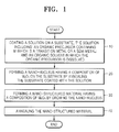
- FIG. 1 is a flow chart illustrating a method of forming an oxide-based nano-structured material according to an embodiment of the present invention.
- a solution is coated on a substrate, the solution including: an organic precursor containing M which is a transition metal or a semi metal; and an organic solvent in which the organic precursor is dissolved.
- an organic precursor containing M is mixed with an organic solvent to prepare the solution,
- the volume ratio between the organic precursor and an alcohol-based organic solvent is in the range of about 1:1 to 1,5000 in the solution,
- the organic precursor may be M(CH 3 COO) 2 ⁇ 2H 2 O.
- M may be a transition metal selected from the group consisting of Ti, V, Cr, Zn, Y, Zr and Nb, or a semi metal selected from the group consisting of Si, Ge and As.
- the organic solvent may be an alcohol-based organic solvent such as methanol and ethanol.
- the solution may be coated on the substrate using dipping, spin coating, or spray coating.
- the substrate may be formed of Al 2 O 3 , quartz, Si, GaN, or glass.
- the following process can be performed.
- the organic precursor containing M for example, M(CH 3 COO) 2 ⁇ 2H 2 O is dissolved in the alcohol-based organic solvent such as methanol, ethanol, and isopropyl alcohol (IPA) in a volume ratio between 1:1 and 1:5000, and the solution is stirred at room temperature for about 1 minute to 24 hours.
- the substrate is dipped in the stirred solution for about 1 second to 1 hour to uniformly coat the substrate with the solution.
- the substrate is taken out of the solution.
- the thickness of the thin film formed of the solution on the substrate may be adjusted to about 1 to 1000 nm by controlling the dipping time or other conditions
- the solution when the solution is coated on the substrate using the spin coating, about 0.01 to 100 ml of the solution is dropped on the substrate using a pipette while rotating the substrate at about 100 to 10000 rpm to form a thin film on the substrate.
- the solution when the solution is coated on the substrate using the spray coating, the solution can be thinly coated on the substrate using appropriate spray equipment.
- M(CH 3 COO) 2 ⁇ 2H 2 O is used as the organic precursor containing M and an alcohol-based organic solvent is used as the organic solvent, but the invention is not limited thereto.
- the organic precursor may be M(CH 3 COO) 2 ⁇ H 2 O, M(CH 3 COO) 2 , M(CH 3 ) 2 , M(C 2 H 5 ) 2 , M(C 5 H 7 O 2 ) 2 , or the like.
- the organic solvent may be a non-alcohol-based organic solvent.
- the substrate coated with the solution is annealed to form a nano-nucleus having a composition of MxOy in which x is an integer of 1 to 3 and y is an integer of 1 to 6 on the substrate.
- the annealing to form the nano-nucleus may be performed using a hot plate, a furnace, a vacuum chamber, or the like The annealing may be performed at a temperature in the range of about 50 to 500°C for about 1 second to 1 hour. While the organic solvent in the solution coated on the substrate is volatilized through the annealing, a plurality of nano-nuclei of an oxide having a uniform size formed of a transition metal or a semi metal which are dissolved in the solution are formed.
- the nano-nuclei may have about several to several tens of nanometers.
- a nano-nuclei including ZnO is formed on the substrate.
- the nano-nuclei grow to form a nano-structured material having a composition of MxOy in which x is an integer of 1 to 3 and y is an integer of 1 to 6 on the substrate to a desired size.
- a physiochemical process such as sputtering, thermal chemical vapor deposition, metal-organic CVD (MOCVD), vapor liquid solid epitaxial (VSLE), pulsed laser deposition (PLD), and sol-gel process may be used to grow the nano-nuclei.
- MOCVD metal-organic CVD
- VSLE vapor liquid solid epitaxial
- PLD pulsed laser deposition
- sol-gel process may be used to grow the nano-nuclei.
- a reaction precursor including M may be supplied to the nano-nuclei as a source material for the growth of the nano-nuclei.
- M a source material for the growth of the nano-nuclei.
- Zn(CH 3 ) 2 as an M source material, and O 2 gas as an O source can each be supplied to the substrate when using MOCVD for the growth of the nano-nuclei.
- Ar can be used as a carrier gas.
- the nano-structured material grown from the nano-nuclei may have various shapes such as a nano-wire shape, a nano-rod shape, and a nano-wall shape.
- the nano-structured material is annealed.
- the annealing of the nano-structured material may be performed using a hot plate, a furnace, a vacuum chamber, or the like.
- the annealing may be performed at a temperature in the range of about 100 to 1200°C for about 1 minute to 24 hours.
- the temperature at which the nano-structured material is annealed in this operation may be higher than that at which the substrate is annealed in operation 20.
- the annealing time for the nano-structured material may be longer than that for the substrate in operation 20.
- those conditions are not necessary, and the annealing can be performed on conditions contrary to those described above to obtain the purpose of the annealing in operation 40.
- the annealing of the nano-structured material may be performed in normal atmospheric conditions or a vacuum chamber containing oxygen.
- the oxide-based nano-structured material having a uniform composition can be obtained since lack of oxygen in the nano-structured material is compensated by annealing of the nano-structured material. Further, a lattice-matched nano-structured material can be obtained due to improvement in crystallinity of the nano-structured material, and thus the crystal quality can be improved.
- the nano-structured material having excellent crystallinity can be employed as a component in diodes or optoelectronic devices to improve electrical and optical properties of the devices.
- an oxide-based nano-structured material of the present invention a nano-nucleus having the same composition as the desired oxide-based nano-structured material is used to grow the oxide-based nano-structured material, and the nano-nucleus is formed using a wet chemical process. Since the oxide-based nano-structured material according to the present invention is grown using a nano-nucleus having the same composition as the desired oxide-based nano-structured material, the nano-structured material does not include impurities.
- the process of forming the nano-structured material can be simplified, and the costs therefor can be lowered compared to conventional methods" Further, the crystal quality can be improved by realizing the nano-structured material having a uniform composition, and the injection of a doping element can be easily controlled when the resulting nano-structured material is doped.
- the oxide-based nano-structured material formed according to the present invention can provide a uniform connection when applied to minimized and integrated electronic circuits, and also provide stable electrical and optical properties.
- the oxide-based nano-structured material formed according to the present invention can be widely applied to the fields of nano-electronic devices such as FETs, SETs, photodiodes, biochemical sensors, and logic circuits, solar batteries, or displays.
- nano-electronic devices such as FETs, SETs, photodiodes, biochemical sensors, and logic circuits, solar batteries, or displays.
Landscapes
- Chemical & Material Sciences (AREA)
- Engineering & Computer Science (AREA)
- Materials Engineering (AREA)
- Metallurgy (AREA)
- Organic Chemistry (AREA)
- Crystallography & Structural Chemistry (AREA)
- Chemical Kinetics & Catalysis (AREA)
- General Chemical & Material Sciences (AREA)
- Mechanical Engineering (AREA)
- Nanotechnology (AREA)
- Inorganic Chemistry (AREA)
- Physics & Mathematics (AREA)
- Thermal Sciences (AREA)
- Manufacturing & Machinery (AREA)
- Dispersion Chemistry (AREA)
- Condensed Matter Physics & Semiconductors (AREA)
- General Physics & Mathematics (AREA)
- Composite Materials (AREA)
- Ceramic Engineering (AREA)
- Liquid Deposition Of Substances Of Which Semiconductor Devices Are Composed (AREA)
- Thin Film Transistor (AREA)
Abstract
Description
- This application claims the benefit of
Korean Patent Application Nos. 10-2006-0122630, filed on December 5, 2006 10-2007-0036582, filed on April 13, 2007 - The present invention relates to a method of forming an oxide-based nano-structured material, and more particularly, to a method of forming a nano-structured material using an oxide of a transition metal or a semi metal.
- Oxide-based nano-structured materials containing a metal or non-metal element are potentially applicable to the field of nano-electronic devices such as field effect transistors (FETs), single electron transistors (SETs), photodiodes, biochemical sensors, and logic circuits, Accordingly, research on properties of nano-structured materials and methods of forming the same have been conducted in various technical fields.
- According to a conventional method of forming an oxide-based nano-structured material, a noble metal such as Au, Ag, Pd, and Pt is deposited on a substrate using sputtering or thermal evaporation to form a nano-level noble metal thin film, and then the substrate is annealed to form noble metal particles or a noble metal cluster. Then, an oxide-based nano-structured material is grown from the substrate using the noble metal particles or the noble metal cluster as a nucleus through a physical or chemical process.
- However, this conventional method of forming an oxide-based nano-structured material is complicated and requires a large area substrate, and thus also requires large-scale equipment for the growth of the oxide-based nano-structured material. Further, as a result of the complicated process of forming the noble metal nano particles which function as the nucleus, and then growing the oxide-based nano-structured material therefrom, the noble metal remains in the resulting oxide-based nano-structured material as an impurity. In addition, the manufacturing costs increase due to the noble metal. Therefore, mass production of the oxide-based nano-structured material is limited.
- In addition, a connection between the noble metal particles or the noble metal cluster and the oxide-based nano-structured material is incomplete since they have different compositions, and a dopant is not easily injected into the resulting nano-structure. In particular, although the material itself used in the nano-structured material has excellent electrical properties, it is not easy to control growth rate, size, and shape of the nano-structured material according to a plane index of the noble metal used as the nucleus. Thus, the oxide-based nano-structured material cannot have a uniform composition, shape and size, and as such is unable to have stable properties.. Therefore, since the oxide-based nano-structured material formed according to the conventional method provides unstable electrical properties, application to integrated high-speed electronic circuits is limited..
- The present invention provides a method of forming an oxide-based nano-structured material for realizing a oxide-based nano-structured material having a uniform composition at low costs by growing the oxide-based nano-structured material without impurities, and providing stable electrical properties appropriate for the application to be minimized and integrated electronic circuits.
- According to an aspect of the present invention, there is provided a method of forming an oxide-based nano-structured material, the method including:
- coating a solution on a substrate, the solution including (a) an organic precursor containing M which is a transition metal or a semi metal and (b) an organic solvent dissolving the organic precursor;
- forming a nano-nucleus having a composition of MxOy in which x is an integer of 1 to 3 and y is an integer of 1 to 6 on the substrate by annealing the substrate coated with the solution;
- forming a nano-structured material having a composition of MxOy in which x is an integer of 1 to 3 and y is an integer of 1 to 6 by growing the nano-nucleus while supplying a reaction precursor containing M into the nano-nucleus; and
- annealing the nano-structured material.
- The solution may be prepared by mixing the organic precursor and an alcohol-based organic solvent in a volume ratio of between 1:1 and 1:5000.
- The coating of the solution on the substrate may be performed using dipping, spin coating, or spray coating.
- The annealing of the substrate coated with the solution may be performed at a temperature in the range of 50 to 500°C for 1 second to 1 hour.
- The forming a nano-structured material may be performed using a process selected from the group consisting of sputtering, thermal chemical vapor deposition, metal-organic CVD (MOCVD), vapor liquid solid epitaxial (VSLE), pulsed laser deposition (PLD), and sol-gel process to grow the nano-nucleus.
- The annealing the nano-structured material may be performed at a temperature in the range of 100 to 1200°C for 1 minute to 24 hours.
- The nano-structured material may have a nano-wire shape, a nano-rod shape, or a nano-wall shape.
- According to a method of forming an oxide-based nano-structured material of the present invention, the nano-structured material does not include an impurity since the oxide-based nano-structured material is grown using a nano-nucleus having the same composition as the desired oxide-based nano-structured material. Further, an oxide-based nano-structured material having excellent crystalline properties can be formed through a simple process at low manufacturing costs by employing a wet chemical process to form the nano-nucleus. Therefore, the oxide-based nano-structured material formed according to the present invention can provide a uniform connection when applied to minimized and integrated electronic circuits, and also provide stable electrical and optical properties..
- The above and other features and advantages of the present invention will become more apparent by describing in detail exemplary embodiments thereof with reference to the attached drawing in which:
-
FIG. 1 is a flow chart illustrating a method of forming an oxide-based nano-structured material according to an embodiment of the present invention. - Hereinafter, the present invention will now be described more fully with reference to the accompanying drawing, in which exemplary embodiments of the invention are shown. The invention may, however, be embodied in many different forms and should not be construed as being limited to the embodiments set forth herein; rather, these embodiments are provided so that this disclosure will be thorough and complete, and will fully convey the concept of the invention to those skilled in the art.
-
FIG. 1 is a flow chart illustrating a method of forming an oxide-based nano-structured material according to an embodiment of the present invention. - Referring to
FIG. 1 , inoperation 10, a solution is coated on a substrate, the solution including: an organic precursor containing M which is a transition metal or a semi metal; and an organic solvent in which the organic precursor is dissolved. - For this, an organic precursor containing M is mixed with an organic solvent to prepare the solution, The volume ratio between the organic precursor and an alcohol-based organic solvent is in the range of about 1:1 to 1,5000 in the solution,
- The organic precursor may be M(CH3COO)2·2H2O. Here, M may be a transition metal selected from the group consisting of Ti, V, Cr, Zn, Y, Zr and Nb, or a semi metal selected from the group consisting of Si, Ge and As.
- The organic solvent may be an alcohol-based organic solvent such as methanol and ethanol.
- The solution may be coated on the substrate using dipping, spin coating, or spray coating. The substrate may be formed of Al2O3, quartz, Si, GaN, or glass.
- When the solution is coated using the dipping, for example, the following process can be performed. First, the organic precursor containing M, for example, M(CH3COO)2·2H2O is dissolved in the alcohol-based organic solvent such as methanol, ethanol, and isopropyl alcohol (IPA) in a volume ratio between 1:1 and 1:5000, and the solution is stirred at room temperature for about 1 minute to 24 hours. Then, the substrate is dipped in the stirred solution for about 1 second to 1 hour to uniformly coat the substrate with the solution. Then, the substrate is taken out of the solution. The thickness of the thin film formed of the solution on the substrate may be adjusted to about 1 to 1000 nm by controlling the dipping time or other conditions
- For example, when the solution is coated on the substrate using the spin coating, about 0.01 to 100 ml of the solution is dropped on the substrate using a pipette while rotating the substrate at about 100 to 10000 rpm to form a thin film on the substrate.
- Also for example, when the solution is coated on the substrate using the spray coating, the solution can be thinly coated on the substrate using appropriate spray equipment.
- In this embodiment, M(CH3COO)2·2H2O is used as the organic precursor containing M and an alcohol-based organic solvent is used as the organic solvent, but the invention is not limited thereto. For example, the organic precursor may be M(CH3COO)2·H2O, M(CH3COO)2, M(CH3)2, M(C2H5)2, M(C5H7O2)2, or the like. Further, the organic solvent may be a non-alcohol-based organic solvent.
- In
operation 20, the substrate coated with the solution is annealed to form a nano-nucleus having a composition of MxOy in which x is an integer of 1 to 3 and y is an integer of 1 to 6 on the substrate. - The annealing to form the nano-nucleus may be performed using a hot plate, a furnace, a vacuum chamber, or the like The annealing may be performed at a temperature in the range of about 50 to 500°C for about 1 second to 1 hour. While the organic solvent in the solution coated on the substrate is volatilized through the annealing, a plurality of nano-nuclei of an oxide having a uniform size formed of a transition metal or a semi metal which are dissolved in the solution are formed. The nano-nuclei may have about several to several tens of nanometers.
- For example, when Zn(CH3COO)2·2H2O is used as the organic precursor, a nano-nuclei including ZnO is formed on the substrate.
- In
operation 30, the nano-nuclei grow to form a nano-structured material having a composition of MxOy in which x is an integer of 1 to 3 and y is an integer of 1 to 6 on the substrate to a desired size. - A physiochemical process such as sputtering, thermal chemical vapor deposition, metal-organic CVD (MOCVD), vapor liquid solid epitaxial (VSLE), pulsed laser deposition (PLD), and sol-gel process may be used to grow the nano-nuclei.
- While the nano-nuclei grow, a reaction precursor including M may be supplied to the nano-nuclei as a source material for the growth of the nano-nuclei. For example, Zn(CH3)2 as an M source material, and O2 gas as an O source can each be supplied to the substrate when using MOCVD for the growth of the nano-nuclei. Here, Ar can be used as a carrier gas.
- The nano-structured material grown from the nano-nuclei may have various shapes such as a nano-wire shape, a nano-rod shape, and a nano-wall shape.
- In
operation 40, the nano-structured material is annealed. - The annealing of the nano-structured material may be performed using a hot plate, a furnace, a vacuum chamber, or the like. The annealing may be performed at a temperature in the range of about 100 to 1200°C for about 1 minute to 24 hours. The temperature at which the nano-structured material is annealed in this operation may be higher than that at which the substrate is annealed in
operation 20. Further, the annealing time for the nano-structured material may be longer than that for the substrate inoperation 20. However, those conditions are not necessary, and the annealing can be performed on conditions contrary to those described above to obtain the purpose of the annealing inoperation 40. The annealing of the nano-structured material may be performed in normal atmospheric conditions or a vacuum chamber containing oxygen. - The oxide-based nano-structured material having a uniform composition can be obtained since lack of oxygen in the nano-structured material is compensated by annealing of the nano-structured material. Further, a lattice-matched nano-structured material can be obtained due to improvement in crystallinity of the nano-structured material, and thus the crystal quality can be improved. The nano-structured material having excellent crystallinity can be employed as a component in diodes or optoelectronic devices to improve electrical and optical properties of the devices.
- According to a method of forming an oxide-based nano-structured material of the present invention, a nano-nucleus having the same composition as the desired oxide-based nano-structured material is used to grow the oxide-based nano-structured material, and the nano-nucleus is formed using a wet chemical process. Since the oxide-based nano-structured material according to the present invention is grown using a nano-nucleus having the same composition as the desired oxide-based nano-structured material, the nano-structured material does not include impurities. Thus, the process of forming the nano-structured material can be simplified, and the costs therefor can be lowered compared to conventional methods" Further, the crystal quality can be improved by realizing the nano-structured material having a uniform composition, and the injection of a doping element can be easily controlled when the resulting nano-structured material is doped. The oxide-based nano-structured material formed according to the present invention can provide a uniform connection when applied to minimized and integrated electronic circuits, and also provide stable electrical and optical properties.
- The oxide-based nano-structured material formed according to the present invention can be widely applied to the fields of nano-electronic devices such as FETs, SETs, photodiodes, biochemical sensors, and logic circuits, solar batteries, or displays.
- While the present invention has been particularly shown and described with reference to exemplary embodiments thereof, it will be understood by those of ordinary skill in the art that various changes in form and details may be made therein without departing from the spirit and scope of the present invention as defined by the following claims.
Claims (13)
- A method of forming an oxide-based nano-structured material, the method comprising;coating a solution on a substrate, the solution including (a) an organic precursor containing M which is a transition metal or a semi metal and (b) an organic solvent dissolving the organic precursor;forming a nano-nucleus having a composition of MxOy in which x is an integer of 1 to 3 and y is an integer of 1 to 6 on the substrate by annealing the substrate coated with the solution;forming a nano-structured material having a composition of MxOy in which x is an integer of 1 to 3 and y is an integer of 1 to 6 by growing the nano-nucleus while supplying a reaction precursor containing M into the nano-nucleus; andannealing the nano-structured material.
- The method of claim 1, wherein M is a transition metal selected from the group consisting of Ti, V, Cr, Zn, Y, Zr and Nb.
- The method of claim 1, wherein M is a semi metal selected from the group consisting of Si, Ge and As.
- The method of one of claims 1 to 3, wherein the solution is prepared by mixing M(CH3COO)2·2H2O as the organic precursor and an alcohol-based organic solvent as the organic solvent.
- The method of claim 4, wherein the organic precursor and the alcohol-based organic solvent are mixed in a volume ratio of between 1:1 and 1:5000.
- The method of one of claims 1 to 5, wherein the coating of the solution on the substrate is performed using dipping, spin coating, or spray coating.
- The method of one of claims 1 to 6, wherein the annealing of the substrate coated with the solution is performed at a temperature in the range of 50 to 500°C.
- The method of claim 7, wherein the annealing of the substrate coated with the solution is performed for a time in the range of 1 second to 1 hour.
- The method of one of claims 1 to 8, wherein the forming of a nano-structured material is performed using a process selected from the group consisting of sputtering, thermal chemical vapor deposition, metal-organic CVD (MOCVD), vapor liquid solid epitaxial (VSLE), pulsed laser deposition (PLD), and a sol-gel process to grow the nano-nucleus.
- The method of one of claims 1 to 9, wherein the annealing of the nano-structured material is performed at a temperature in the range of 100 to 1200°C.
- The method of claim 10, wherein the annealing the nano-structured material is performed for a time in the range of 1 minute to 24 hours.
- The method of one of claims 1 to 11, wherein the nano-structured material has a nano-wire shape, a nano-rod shape, or a nano-wall shape..
- The method of one of claims 1 to 12, wherein the substrate is formed of one selected from the group consisting of Al2O3, quartz, Si, GaN, and glass.
Applications Claiming Priority (2)
| Application Number | Priority Date | Filing Date | Title |
|---|---|---|---|
| KR20060122630 | 2006-12-05 | ||
| KR1020070036582A KR100825765B1 (en) | 2006-12-05 | 2007-04-13 | Method for producing oxide-based nanostructures |
Publications (1)
| Publication Number | Publication Date |
|---|---|
| EP1930469A1 true EP1930469A1 (en) | 2008-06-11 |
Family
ID=38701669
Family Applications (1)
| Application Number | Title | Priority Date | Filing Date |
|---|---|---|---|
| EP07116733A Withdrawn EP1930469A1 (en) | 2006-12-05 | 2007-09-19 | Method of forming oxide-based nano-structured material |
Country Status (2)
| Country | Link |
|---|---|
| EP (1) | EP1930469A1 (en) |
| GB (1) | GB2444586A (en) |
Cited By (1)
| Publication number | Priority date | Publication date | Assignee | Title |
|---|---|---|---|---|
| WO2014045241A2 (en) | 2012-09-20 | 2014-03-27 | Ecole Polytechnique Federale De Lausanne (Epfl) | Method for hardening a coating of a solar collector element, and elements produced by means of said method |
Citations (2)
| Publication number | Priority date | Publication date | Assignee | Title |
|---|---|---|---|---|
| WO2006004248A1 (en) * | 2004-03-11 | 2006-01-12 | Postech Foundation | Photocatalyst including oxide-based nanomaterial |
| US20060091499A1 (en) * | 2004-10-29 | 2006-05-04 | Sharp Laboratories Of America, Inc. | ALD ZnO seed layer for deposition of ZnO nanostructures on a silicon substrate |
Family Cites Families (1)
| Publication number | Priority date | Publication date | Assignee | Title |
|---|---|---|---|---|
| US20060040168A1 (en) * | 2004-08-20 | 2006-02-23 | Ion America Corporation | Nanostructured fuel cell electrode |
-
2007
- 2007-09-19 EP EP07116733A patent/EP1930469A1/en not_active Withdrawn
- 2007-09-26 GB GB0718766A patent/GB2444586A/en not_active Withdrawn
Patent Citations (2)
| Publication number | Priority date | Publication date | Assignee | Title |
|---|---|---|---|---|
| WO2006004248A1 (en) * | 2004-03-11 | 2006-01-12 | Postech Foundation | Photocatalyst including oxide-based nanomaterial |
| US20060091499A1 (en) * | 2004-10-29 | 2006-05-04 | Sharp Laboratories Of America, Inc. | ALD ZnO seed layer for deposition of ZnO nanostructures on a silicon substrate |
Non-Patent Citations (2)
| Title |
|---|
| JUAN ZHAO ET AL: "Growth of ZnO nanorods by the chemical solution method with assisted electrical field", JOURNAL OF THE AMERICAN CERAMIC SOCIETY AMERICAN CERAMIC SOC USA, vol. 89, no. 8, August 2006 (2006-08-01), pages 2654 - 2659, XP002474586, ISSN: 0002-7820 * |
| OLSON ET AL: "Hybrid photovoltaic devices of polymer and ZnO nanofiber composites", THIN SOLID FILMS, ELSEVIER-SEQUOIA S.A. LAUSANNE, CH, vol. 496, no. 1, 1 February 2006 (2006-02-01), pages 26 - 29, XP005181420, ISSN: 0040-6090 * |
Cited By (1)
| Publication number | Priority date | Publication date | Assignee | Title |
|---|---|---|---|---|
| WO2014045241A2 (en) | 2012-09-20 | 2014-03-27 | Ecole Polytechnique Federale De Lausanne (Epfl) | Method for hardening a coating of a solar collector element, and elements produced by means of said method |
Also Published As
| Publication number | Publication date |
|---|---|
| GB0718766D0 (en) | 2007-11-07 |
| GB2444586A (en) | 2008-06-11 |
Similar Documents
| Publication | Publication Date | Title |
|---|---|---|
| US20080268656A1 (en) | Method of forming oxide-based nano-structured material | |
| Galazka | β-Ga2O3 for wide-bandgap electronics and optoelectronics | |
| CN112359421B (en) | Method for preparing layered bismuth-oxygen-selenium semiconductor film by reverse airflow method | |
| Hung et al. | Low-temperature solution approach toward highly aligned ZnO nanotip arrays | |
| US7767140B2 (en) | Method for manufacturing zinc oxide nanowires and device having the same | |
| US8173205B2 (en) | Method for fabricating ZnO thin films | |
| US8513641B2 (en) | Core-shell nanowire comprising silicon rich oxide core and silica shell | |
| CN102037165A (en) | Method and Thin Film Devices for Fabricating Nanostructures on Metal Oxide Substrates | |
| CN1328410C (en) | Low-pressure metal organic chemical vapour phase depositing apparatus for zinc oxide and process thereof | |
| CN102051593B (en) | Method and device for epitaxially growing metal oxide transparent conductive film | |
| CN109437124B (en) | Method for synthesizing single-layer transition metal chalcogenide | |
| CN100487909C (en) | Heterogeneous p-n nano-line array, its production and use | |
| WO2008117932A1 (en) | Method of manufacturing oxide-based nano-structured material | |
| Prakash et al. | Molecular Beam Epitaxy for Oxide | |
| KR100456016B1 (en) | A process for preparing a zinc oxide nanowire by metal organic chemical vapor deposition and a nanowire prepared therefrom | |
| GB2444586A (en) | Method of forming oxide based nano structures | |
| CN101798672A (en) | Method for preparing P-type zinc oxide film from in situ low-pressure oxidized aluminum-doped zinc nitride | |
| GB2482915A (en) | Growing Silicon by Plasma Enhanced Chemical Vapour Deposition | |
| CN101693528B (en) | Method for growing ZnSe monocrystal nanowire | |
| KR101486955B1 (en) | A method for fabricating aligned oxide semiconductor wire patterns and electronic devices with the same | |
| KR102726926B1 (en) | Method for preparing thin film of three-dimensional transition metal dichalcogenide having high uniformity | |
| JP5042636B2 (en) | Functional element | |
| KR100536483B1 (en) | Zinc oxide nanoneedle, preparation thereof, and electronic device using same | |
| CN114672767A (en) | A kind of chemical vapor deposition preparation method of large-scale platinum ditelluride | |
| CN118649858B (en) | A wafer-level ferromagnetic metal-organic thin film and its preparation method |
Legal Events
| Date | Code | Title | Description |
|---|---|---|---|
| PUAI | Public reference made under article 153(3) epc to a published international application that has entered the european phase |
Free format text: ORIGINAL CODE: 0009012 |
|
| AK | Designated contracting states |
Kind code of ref document: A1 Designated state(s): AT BE BG CH CY CZ DE DK EE ES FI FR GB GR HU IE IS IT LI LT LU LV MC MT NL PL PT RO SE SI SK TR |
|
| AX | Request for extension of the european patent |
Extension state: AL BA HR MK RS |
|
| 17P | Request for examination filed |
Effective date: 20081209 |
|
| AKX | Designation fees paid |
Designated state(s): AT BE BG CH CY CZ DE DK EE ES FI FR GB GR HU IE IS IT LI LT LU LV MC MT NL PL PT RO SE SI SK TR |
|
| 17Q | First examination report despatched |
Effective date: 20090217 |
|
| STAA | Information on the status of an ep patent application or granted ep patent |
Free format text: STATUS: THE APPLICATION IS DEEMED TO BE WITHDRAWN |
|
| 18D | Application deemed to be withdrawn |
Effective date: 20090630 |