EP1930216A1 - Wire beam - Google Patents
Wire beam Download PDFInfo
- Publication number
- EP1930216A1 EP1930216A1 EP06077193A EP06077193A EP1930216A1 EP 1930216 A1 EP1930216 A1 EP 1930216A1 EP 06077193 A EP06077193 A EP 06077193A EP 06077193 A EP06077193 A EP 06077193A EP 1930216 A1 EP1930216 A1 EP 1930216A1
- Authority
- EP
- European Patent Office
- Prior art keywords
- conductors
- mid
- wire beam
- support member
- moulding
- Prior art date
- Legal status (The legal status is an assumption and is not a legal conclusion. Google has not performed a legal analysis and makes no representation as to the accuracy of the status listed.)
- Withdrawn
Links
- 238000000034 method Methods 0.000 claims abstract description 55
- 230000008569 process Effects 0.000 claims abstract description 30
- 239000004020 conductor Substances 0.000 claims abstract description 26
- 238000004519 manufacturing process Methods 0.000 claims abstract description 21
- 238000004070 electrodeposition Methods 0.000 claims abstract description 6
- 238000000465 moulding Methods 0.000 description 18
- RYGMFSIKBFXOCR-UHFFFAOYSA-N Copper Chemical compound [Cu] RYGMFSIKBFXOCR-UHFFFAOYSA-N 0.000 description 15
- 229920005989 resin Polymers 0.000 description 15
- 239000011347 resin Substances 0.000 description 15
- 229910052802 copper Inorganic materials 0.000 description 14
- 239000010949 copper Substances 0.000 description 14
- 238000002347 injection Methods 0.000 description 10
- 239000007924 injection Substances 0.000 description 10
- 238000007747 plating Methods 0.000 description 9
- 239000000758 substrate Substances 0.000 description 8
- 238000001746 injection moulding Methods 0.000 description 6
- 239000002184 metal Substances 0.000 description 6
- 229910052751 metal Inorganic materials 0.000 description 6
- 239000003054 catalyst Substances 0.000 description 5
- 239000004033 plastic Substances 0.000 description 5
- 229920000642 polymer Polymers 0.000 description 5
- 239000000126 substance Substances 0.000 description 5
- 238000013461 design Methods 0.000 description 4
- 238000004049 embossing Methods 0.000 description 4
- 239000010410 layer Substances 0.000 description 4
- 238000012986 modification Methods 0.000 description 4
- 230000004048 modification Effects 0.000 description 4
- 230000008901 benefit Effects 0.000 description 3
- 238000005516 engineering process Methods 0.000 description 3
- 230000009467 reduction Effects 0.000 description 3
- 238000012552 review Methods 0.000 description 3
- 238000012546 transfer Methods 0.000 description 3
- PXHVJJICTQNCMI-UHFFFAOYSA-N Nickel Chemical compound [Ni] PXHVJJICTQNCMI-UHFFFAOYSA-N 0.000 description 2
- 239000000654 additive Substances 0.000 description 2
- 230000000996 additive effect Effects 0.000 description 2
- 238000005530 etching Methods 0.000 description 2
- 239000011888 foil Substances 0.000 description 2
- 238000003384 imaging method Methods 0.000 description 2
- 239000000976 ink Substances 0.000 description 2
- 150000002739 metals Chemical class 0.000 description 2
- 238000012545 processing Methods 0.000 description 2
- 229920001169 thermoplastic Polymers 0.000 description 2
- 239000004416 thermosoftening plastic Substances 0.000 description 2
- BQCADISMDOOEFD-UHFFFAOYSA-N Silver Chemical compound [Ag] BQCADISMDOOEFD-UHFFFAOYSA-N 0.000 description 1
- ATJFFYVFTNAWJD-UHFFFAOYSA-N Tin Chemical compound [Sn] ATJFFYVFTNAWJD-UHFFFAOYSA-N 0.000 description 1
- 230000004913 activation Effects 0.000 description 1
- 239000000853 adhesive Substances 0.000 description 1
- 230000001070 adhesive effect Effects 0.000 description 1
- 239000003518 caustics Substances 0.000 description 1
- 238000010276 construction Methods 0.000 description 1
- 239000011889 copper foil Substances 0.000 description 1
- 238000005260 corrosion Methods 0.000 description 1
- 230000007797 corrosion Effects 0.000 description 1
- 238000011161 development Methods 0.000 description 1
- 238000007772 electroless plating Methods 0.000 description 1
- 238000002474 experimental method Methods 0.000 description 1
- 229910052737 gold Inorganic materials 0.000 description 1
- 239000010931 gold Substances 0.000 description 1
- 238000010348 incorporation Methods 0.000 description 1
- 238000003780 insertion Methods 0.000 description 1
- 230000037431 insertion Effects 0.000 description 1
- 239000000463 material Substances 0.000 description 1
- 239000002991 molded plastic Substances 0.000 description 1
- 238000010137 moulding (plastic) Methods 0.000 description 1
- 229910052759 nickel Inorganic materials 0.000 description 1
- 239000002861 polymer material Substances 0.000 description 1
- 239000002952 polymeric resin Substances 0.000 description 1
- 238000007639 printing Methods 0.000 description 1
- 239000011241 protective layer Substances 0.000 description 1
- 229910052709 silver Inorganic materials 0.000 description 1
- 239000004332 silver Substances 0.000 description 1
- 229920003002 synthetic resin Polymers 0.000 description 1
- 239000013585 weight reducing agent Substances 0.000 description 1
Images
Classifications
-
- B—PERFORMING OPERATIONS; TRANSPORTING
- B60—VEHICLES IN GENERAL
- B60R—VEHICLES, VEHICLE FITTINGS, OR VEHICLE PARTS, NOT OTHERWISE PROVIDED FOR
- B60R16/00—Electric or fluid circuits specially adapted for vehicles and not otherwise provided for; Arrangement of elements of electric or fluid circuits specially adapted for vehicles and not otherwise provided for
- B60R16/02—Electric or fluid circuits specially adapted for vehicles and not otherwise provided for; Arrangement of elements of electric or fluid circuits specially adapted for vehicles and not otherwise provided for electric constitutive elements
- B60R16/0207—Wire harnesses
Definitions
- the invention concerns a wire beam configuration, e.g. to be used in a vehicle.
- Wire beams in vehicles often include a carrier or support body, on which or in which a plurality of isolated copper wires are mounted.
- Wire beams are rather large and laborious products. The assembly times are rather long. The reliability and serviceability of complex wire beams may be problematic in some cases.
- One aim of the present invention is to provide an improved wire beam (or wire tree) manufacture method, having a shorter processing time and resulting in a more reliable product.
- Another aim of the invention is to provide an improved and more reliable wire beam.
- the method for manufacturing a wire beam comprising a support member and a number of conductors, preferrably comprises to incorporate or integrate the conductors on or in the support member by means of a so-called moulded interconnect device (MID) manufacture method.
- MID moulded interconnect device
- a wire beam according to the invention comprising a support member and a number of conductors, preferably is a so-called moulded interconnect device (MID) the conductors of which being incorporated at, on or in of the support member.
- MID moulded interconnect device
- MIDs Moulded Interconnect devices
- MIDs can be defined as an injection moulded thermoplastic substrate which incorporates a conductive circuit pattern, and integrates mechanical and electrical functions. They are usually three dimensional and a variety of techniques may be used to apply the conductors and components. The technology has made significant advances in recent years, particularly the development of high-temperature resins and using rapid prototyping techniques to generate pre-production examples, but requirements for multilayers, high component densities and plated-through holes will continue to be met by conventional planar printed circuit board technology. A review can be found at http://www.primefaraday.org.uk/technology-watch/technology-reviews/moulded-interconnect-devices.pdf
- the intented conducting tracks are preprocessed (e.g. by laser surface treating) and subsequently (electroless) metallized.
- the conductive tracks applied to the synthetic carrier (support member) have a flat shape. No assembly is needed anymore.
- MID is mainly used for small products and for low power applications. Using MID technology for large products and/or high power applications in e.g. automotive, aviation etc. is not known from the prior art.
- MID based wire beams included reduction of the assembly time, reliability, weight reduction, cost reduction and space reduction.
- Application areas include all areas in which wiring beams (trees) are used in combination with high(er) power, e.g. automotive, aviation, aerospace.
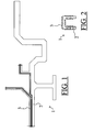
- the wire beam 1 shown in figure 1 comprises a support member 2 and a number of conductors 3.
- the wire beam has the shape of a moulded interconnect device (MID): the conductors 3 are incorporated at the outer or inner (see figure 2 ) surface of the support member 2.
- MID moulded interconnect device
- the wire beam 1 is made by the moulded interconnect device (MID) manufacture method which is known as such, so it may be redundant to discuss several MID techniques. However, for the sake of completeness, below some items of the MID process will be reviewed, referencing to http://www.primefaraday.org.uk/technology-watch/technology-reviews/moulded-interconnect-devices.pdf.
- MID moulded interconnect device
- MIDs can be produced in a variety of ways to suit the application at hand.
- Established methods of manufacture include Single-shot injection moulding, Two-shot moulding and Film Techniques.
- the moulding process is followed by a series of metallizing steps that are very similar to those employed for conventional printed circuitry.
- One of the key techniques utilised in the manufacture of MIDs with fine circuit traces is photoimaging.
- the MID substrate is chemically treated to promote adhesion between the plastic and metal that will be plated on it.
- a thin layer of electroless copper is deposited onto the substrate's surface to make it conductive, followed by the application of an electrophoretic resist resin.
- Two-Shot Moulding uses two separate moulding cycles and usually different polymers to form the component. It requires the construction of different mould cavities for each shot.
- Catalysed resin versions of this process use a polymer that contains a small quantity of plating catalyst.
- the part is designed so that imaging is undertaken during moulding by leaving this catalysed resin exposed on the surface of the final part only where the circuit traces are required. This is accomplished by creating two moulds.
- the first shot is moulded and then inserted into the second mould in which the second resin system forms the final three-dimensional features of the component.
- either the first or second shot resin may be the one containing a plating catalyst.
- a variation of this technique is to use resins which do not contain a plating catalyst.
- the first shot is moulded and chemically treated with a catalyst before moulding the second shot. Copper plating is then undertaken and only the resin that has been chemically treated plates to form circuits.
- two-shot moulding can enable very complex three-dimensional circuitry to be produced, limited only by an ability to mould the component since there are no additional imaging steps involved.
- Plated-through holes can be accommodated, but because circuit design changes usually require mould modifications it is more difficult and expensive to incorporate changes on parts within this process.
- Line and width spacing is limited by the moulding process, and it is generally difficult to achieve spacings as low as other PCB techniques; a typical value is 0.25mm. It is the least labour-intensive process and generally the easiest to automate for high-volume production. However, tooling costs are high, which means that it is more suited to high-volume production requirements, typically associated with the telecommunications and automotive industries.
- Film techniques have in common the fact that the conducting material starts out as a separate flexible film and is subsequently attached to an injection-moulded plastic substrate.
- the conductors are usually formed from copper laminate, foil or silver conductive inks on a carrier. Typical film processes are the Capture Process, the Transfer Process and Hot Stamping.
- the capture process utilises preformed circuits on a flexible carrier, which are inserted into an injection mould.
- the circuits are formed either by printing conductive inks, or by etching copper-clad films.
- Circuits on a flexible carrier are die-cut to shape and can be thermoformed into three dimensions before insertion into the mould.
- Polymeric resin is injected behind the carrier, thus forcing it against the outer surfaces of the mould when the cycle is complete, the carrier with circuit becomes an integral part of a rigid injection moulded item; plating may be used to increase circuit thickness or provide a different metal topcoat, and circuits on the carrier can be single or double-sided (connected by vias in the carrier).
- the transfer process is a variation of the capture process in that the flexible film is peeled away rather than remaining with the moulded part. In this case, the top of the circuits are flush with the moulded surface which can have benefits for applications requiring sliding contacts.
- Hot stamping is another technique that utilises flexible copper foil coated with an adhesive.
- a special embossing die is built incorporating a heated block. The substrate is injection moulded prior to applying the circuit. Foil is pressed onto the polymer surface using this heated die and is simultaneously cut into the shape of the embossing die, thus forming a circuit.
- the plastic surface where the circuit is to be embossed must be comparatively flat or have a smooth, uniform contour so that the embossing die can precisely contact the surface.
- these film processes are more easily applied to relatively flat surfaces but are capable of providing moderately complex three-dimensional circuits using special techniques. Since the circuitry is on a separate carrier it is easy to modify circuit design provided this does not necessitate mould modifications. Track line and width spacing in the region of 0.025mm is no real problem, but is it difficult to provide plated through holes.
- the three-dimensional circuit carrier is injection moulded from a modified polymer material.
- the modification allows laser activation of circuit tracks on the surface of the circuit carrier.
- the activated areas become metalized in a chemical metalisation bath in order to build conductive tracks.
- a number of tracks may - in first instance - be short-circuited at the ends of the wire beams, facilitating to include all or a plurality of conductive tracks together in an electrical circuit which is used to perform electrodeposition (process for applying a galvanic layer using electric current) upon the tracks, viz. to provide them with an additional conductive layer which is thick and robust enough to conduct large currents which may be used in the relevant, e.g. automotive, applications.
- Those short-circuited ends of the conductive tracks may be cut or punched off after the electrodeposition process has been completed.
- the conductive tracks may be covered by a protective layer, e.g. made of a polymer or an anti-corrosive conductor.
Landscapes
- Engineering & Computer Science (AREA)
- Mechanical Engineering (AREA)
- Injection Moulding Of Plastics Or The Like (AREA)
- Manufacturing Of Printed Wiring (AREA)
Abstract
Manufacturing a wire beam (1), comprising a support member (2) and a number of conductors (3). In order to incorporate the conductors on or in the support member the wire beam is manufactured by means of a so-called moulded interconnect device (MID) manufacture process. At least part of the conductors may be shaped, during the MID manufacturing process, as conductors which are conductively interconnected at their ends. The interconnected conductors then may be used as a common electrode during a electrodeposition process in which the conductors are galvanized electrically to provide them with an additional conductive layer. The interconnected ends are removed after completion of the electrodeposition process.
Description
- The invention concerns a wire beam configuration, e.g. to be used in a vehicle.
- Wire beams in vehicles (cars, trucks, aeraoplanes etc.) often include a carrier or support body, on which or in which a plurality of isolated copper wires are mounted. Wire beams are rather large and laborious products. The assembly times are rather long. The reliability and serviceability of complex wire beams may be problematic in some cases.
- One aim of the present invention is to provide an improved wire beam (or wire tree) manufacture method, having a shorter processing time and resulting in a more reliable product. Another aim of the invention is to provide an improved and more reliable wire beam.
- According to the invention the method for manufacturing a wire beam, comprising a support member and a number of conductors, preferrably comprises to incorporate or integrate the conductors on or in the support member by means of a so-called moulded interconnect device (MID) manufacture method.
- Moreover, a wire beam according to the invention, comprising a support member and a number of conductors, preferably is a so-called moulded interconnect device (MID) the conductors of which being incorporated at, on or in of the support member.
- Moulded Interconnect devices (MIDs) can be defined as an injection moulded thermoplastic substrate which incorporates a conductive circuit pattern, and integrates mechanical and electrical functions. They are usually three dimensional and a variety of techniques may be used to apply the conductors and components. The technology has made significant advances in recent years, particularly the development of high-temperature resins and using rapid prototyping techniques to generate pre-production examples, but requirements for multilayers, high component densities and plated-through holes will continue to be met by conventional planar printed circuit board technology. A review can be found at http://www.primefaraday.org.uk/technology-watch/technology-reviews/moulded-interconnect-devices.pdf
- By using MID techniques, the intented conducting tracks are preprocessed (e.g. by laser surface treating) and subsequently (electroless) metallized. The conductive tracks applied to the synthetic carrier (support member) have a flat shape. No assembly is needed anymore. Until now MID is mainly used for small products and for low power applications. Using MID technology for large products and/or high power applications in e.g. automotive, aviation etc. is not known from the prior art.
- The electric current which might be conducted by MID tracks is presumed to be rather restricted. However, experiments, done by applicant, indicate that the limits are much higher than generally presumed until now.
- Advantages of using MID based wire beams included reduction of the assembly time, reliability, weight reduction, cost reduction and space reduction. Application areas include all areas in which wiring beams (trees) are used in combination with high(er) power, e.g. automotive, aviation, aerospace.
-
-
Figure 1 shows a view of an example of a wire beam made by the method according to the invention; -
Figure 2 shows a cross-sectional view of an exemplary wire beam. - The wire beam 1 shown in
figure 1 , comprises asupport member 2 and a number ofconductors 3. The wire beam has the shape of a moulded interconnect device (MID): theconductors 3 are incorporated at the outer or inner (seefigure 2 ) surface of thesupport member 2. - The wire beam 1 is made by the moulded interconnect device (MID) manufacture method which is known as such, so it may be redundant to discuss several MID techniques. However, for the sake of completeness, below some items of the MID process will be reviewed, referencing to
http://www.primefaraday.org.uk/technology-watch/technology-reviews/moulded-interconnect-devices.pdf. - Essentially, MIDs can be produced in a variety of ways to suit the application at hand. Established methods of manufacture include Single-shot injection moulding, Two-shot moulding and Film Techniques.
- In the case of single-shot injection moulding, the moulding process is followed by a series of metallizing steps that are very similar to those employed for conventional printed circuitry. One of the key techniques utilised in the manufacture of MIDs with fine circuit traces is photoimaging. To describe this process in simple terms, the MID substrate is chemically treated to promote adhesion between the plastic and metal that will be plated on it. Typically, a thin layer of electroless copper is deposited onto the substrate's surface to make it conductive, followed by the application of an electrophoretic resist resin. Exposure to ultraviolet light through a photomask - a film that carries the artwork of the required circuit traces - causes the resin to harden where the circuit pattern is required; the unhardened resin is then removed, revealing the underlying electroless copper which is then stripped off via chemical means. In the next stage the hardened resist is also chemically removed to reveal the circuit traces underneath. This leaves the plastic moulding with only the desired circuit pattern.
- The typical process stages for single-shot injection moulding of MIDs are:
- Injection mould the substrate: The part is injection moulded in a platable grade of thermoplastic.
- Electroless plate: The surface is chemically prepared to accept electroless plating and a thin layer of electroless copper is deposited on the entire surface.
- Coat resist: A photosensitive polymer resist is applied over the entire part including through-holes (if any) and three-dimensional features.
- Expose to UV and develop: The moulding is exposed to UV light through a conforming phototool such that the resist hardens. The unexposed resist is then chemically removed in the developing stage.
- Electroplate metals: Copper and metals such as tin/lead or nickel/gold are deposited.
- Strip resist and etch background copper: The resist is removed from unplated areas and the background copper is etched.
- There is a variation of this process which utilises fully additive plating techniques. In this case the entire plastic substrate is copper plated to a specified final thickness before resist is applied. The photomask is designed so that this resist is exposed and hardened only where the circuit tracks are required. After unhardened resist is chemically removed, the entire thickness of copper which has been uncovered is removed, again leaving the plastic substrate with only the desired circuit pattern. However, the copper tracks are still covered with hardened resist, which is then chemically removed so that the circuitry can be finished as required.
- Two-Shot Moulding uses two separate moulding cycles and usually different polymers to form the component. It requires the construction of different mould cavities for each shot. Catalysed resin versions of this process use a polymer that contains a small quantity of plating catalyst. The part is designed so that imaging is undertaken during moulding by leaving this catalysed resin exposed on the surface of the final part only where the circuit traces are required. This is accomplished by creating two moulds. The first shot is moulded and then inserted into the second mould in which the second resin system forms the final three-dimensional features of the component. Depending on part design, either the first or second shot resin may be the one containing a plating catalyst. Chemical treatment is undertaken to promote adhesion between the plastic and the metal plated onto it so that when the moulding is put through an electroless copper plating cycle, only resin containing the catalyst plates and thus creates the circuit pattern. Other electroless metal overlays can be applied if desired, and it is not unusual to employ rotary moulds or robotic handling for two-shot moulding processes.
The process stages therefore are: - Injection mould first shot: A first shot, which usually contains non-catalysed resin, is injection moulded in one cavity in a mould. This produces a first-stage moulding having identifiable areas for placement or incorporation of further moulding material for additional processing.
- Injection mould second shot: The first-stage moulding is inserted into a second cavity where a second shot, generally of platable catalysed resin, is introduced into the mould. This typically produces a moulding with exposed, platable, catalysed resin on its surface, the patterns of which define the required circuit tracks.
- Promote adhesion: As part of the plating process, the moulding undergoes a chemical treatment to enhance the ability of catalysed resin to accept plating.
- Plate the part: The moulding is copper plated to a specified thickness. Metallic or organic finishes may then be applied.
- A variation of this technique is to use resins which do not contain a plating catalyst. In this case the first shot is moulded and chemically treated with a catalyst before moulding the second shot. Copper plating is then undertaken and only the resin that has been chemically treated plates to form circuits.
- So, two-shot moulding can enable very complex three-dimensional circuitry to be produced, limited only by an ability to mould the component since there are no additional imaging steps involved. Plated-through holes can be accommodated, but because circuit design changes usually require mould modifications it is more difficult and expensive to incorporate changes on parts within this process. Line and width spacing is limited by the moulding process, and it is generally difficult to achieve spacings as low as other PCB techniques; a typical value is 0.25mm. It is the least labour-intensive process and generally the easiest to automate for high-volume production. However, tooling costs are high, which means that it is more suited to high-volume production requirements, typically associated with the telecommunications and automotive industries.
- Film techniques have in common the fact that the conducting material starts out as a separate flexible film and is subsequently attached to an injection-moulded plastic substrate. The conductors are usually formed from copper laminate, foil or silver conductive inks on a carrier. Typical film processes are the Capture Process, the Transfer Process and Hot Stamping.
- The capture process utilises preformed circuits on a flexible carrier, which are inserted into an injection mould. The circuits are formed either by printing conductive inks, or by etching copper-clad films. Circuits on a flexible carrier are die-cut to shape and can be thermoformed into three dimensions before insertion into the mould. Polymeric resin is injected behind the carrier, thus forcing it against the outer surfaces of the mould when the cycle is complete, the carrier with circuit becomes an integral part of a rigid injection moulded item; plating may be used to increase circuit thickness or provide a different metal topcoat, and circuits on the carrier can be single or double-sided (connected by vias in the carrier).
- The transfer process is a variation of the capture process in that the flexible film is peeled away rather than remaining with the moulded part. In this case, the top of the circuits are flush with the moulded surface which can have benefits for applications requiring sliding contacts.
- Hot stamping is another technique that utilises flexible copper foil coated with an adhesive. A special embossing die is built incorporating a heated block. The substrate is injection moulded prior to applying the circuit. Foil is pressed onto the polymer surface using this heated die and is simultaneously cut into the shape of the embossing die, thus forming a circuit. It is a relatively simple technique but the plastic surface where the circuit is to be embossed must be comparatively flat or have a smooth, uniform contour so that the embossing die can precisely contact the surface. In general, these film processes are more easily applied to relatively flat surfaces but are capable of providing moderately complex three-dimensional circuits using special techniques. Since the circuitry is on a separate carrier it is easy to modify circuit design provided this does not necessitate mould modifications. Track line and width spacing in the region of 0.025mm is no real problem, but is it difficult to provide plated through holes.
- MID processes like 2-component injection moulding, hot stamping etc., reviewed in the preceding, are already used to manufacture 3D-MIDs. At present the predominantly used processes are two-shot injection moulding, hot embossing, insert moulding and laser structuring (additive and subtractive). The associated high initial manufacturing costs, however, considerably limit the efficiency of these methods for small production runs and design modifications. Prototyping shortly before series production is almost impossible. Moreover, increasing miniaturisation of the circuits on MID components leads to a considerable rise in tooling-up time and expense. A rather novel process, introduced by LPKF (www.lpkf.com), the socalled MID-LDS method (LDS standing for Laser Direct Structuring) is a flexible and economic alternative. According to the LDS process the three-dimensional circuit carrier is injection moulded from a modified polymer material. The modification allows laser activation of circuit tracks on the surface of the circuit carrier. The activated areas become metalized in a chemical metalisation bath in order to build conductive tracks. Advantages of the LDS method are:
- More flexibility because the laser directly transfers the artwork from the computer to the injection-moulded component, so no additional tools or masks are required. Structuring takes place solely on the basis of the existing CAD data.
- Tooling costs significantly reduced because laser-structurable MIDs can be made using 1-component injection moulding.
- Lasers are ideal for the production of ultra-fine structures.
- High cost efficiency for fine structures and small to medium production runs in particular.
- Highly pro-environment because no caustic or etching chemicals are used.
- According to a preferred and more elaborated embodiment of the invention a number of tracks may - in first instance - be short-circuited at the ends of the wire beams, facilitating to include all or a plurality of conductive tracks together in an electrical circuit which is used to perform electrodeposition (process for applying a galvanic layer using electric current) upon the tracks, viz. to provide them with an additional conductive layer which is thick and robust enough to conduct large currents which may be used in the relevant, e.g. automotive, applications. Those short-circuited ends of the conductive tracks may be cut or punched off after the electrodeposition process has been completed.
- To protect the conductive tracks (e.g. to be used in trucks etc.) against corrosion etc., the conductive tracks may be covered by a protective layer, e.g. made of a polymer or an anti-corrosive conductor.
Claims (5)
- Method for manufacturing a wire beam (1), comprising a support member (2) and a number of conductors (3), the method comprising to incorporate the conductors at, on or in the support member by means of a so-called moulded interconnect device (MID) manufacturing process.
- Method according to claim 1, at least part of the conductors being shaped, during the MID manufacturing process, as conductors which are conductively interconnected at their ends, the interconnected conductors being used as a common electrode during a consecutive electrodeposition process in which the conductors are galvanized electrically to provide them with an additional conductive layer; the interconnected ends being removed after completion of the electrodeposition process.
- Wire beam (1), comprising a support member (2) and a number of conductors (3), the wire beam being a so-called moulded interconnect device (MID) the conductors of which being incorporated at, on or in of the support member.
- Wire beam according to claim 3, at least part of the conductors comprising an additional conductive layer.
- Wire beam according to claim 3 or 4, at least part of the conductors comprising an anti-corrosive layer.
Priority Applications (4)
| Application Number | Priority Date | Filing Date | Title |
|---|---|---|---|
| EP06077193A EP1930216A1 (en) | 2006-12-07 | 2006-12-07 | Wire beam |
| PCT/NL2007/050618 WO2008069657A1 (en) | 2006-12-07 | 2007-12-04 | Wire beam |
| EP07851878A EP2099651A1 (en) | 2006-12-07 | 2007-12-04 | Wire beam |
| US12/517,829 US20100012372A1 (en) | 2006-12-07 | 2007-12-04 | Wire Beam |
Applications Claiming Priority (1)
| Application Number | Priority Date | Filing Date | Title |
|---|---|---|---|
| EP06077193A EP1930216A1 (en) | 2006-12-07 | 2006-12-07 | Wire beam |
Publications (1)
| Publication Number | Publication Date |
|---|---|
| EP1930216A1 true EP1930216A1 (en) | 2008-06-11 |
Family
ID=37950618
Family Applications (2)
| Application Number | Title | Priority Date | Filing Date |
|---|---|---|---|
| EP06077193A Withdrawn EP1930216A1 (en) | 2006-12-07 | 2006-12-07 | Wire beam |
| EP07851878A Withdrawn EP2099651A1 (en) | 2006-12-07 | 2007-12-04 | Wire beam |
Family Applications After (1)
| Application Number | Title | Priority Date | Filing Date |
|---|---|---|---|
| EP07851878A Withdrawn EP2099651A1 (en) | 2006-12-07 | 2007-12-04 | Wire beam |
Country Status (3)
| Country | Link |
|---|---|
| US (1) | US20100012372A1 (en) |
| EP (2) | EP1930216A1 (en) |
| WO (1) | WO2008069657A1 (en) |
Cited By (4)
| Publication number | Priority date | Publication date | Assignee | Title |
|---|---|---|---|---|
| EP2168818A1 (en) | 2008-09-30 | 2010-03-31 | Sistema S.r.l. | Device for electrifying actuator assemblies and manufacturing method associated therewith |
| EP2178351A1 (en) * | 2008-10-15 | 2010-04-21 | Nederlandse Organisatie voor toegepast-natuurwetenschappelijk Onderzoek TNO | Method for the manufacture of products including conductive tracks. |
| EP2171796A4 (en) * | 2007-07-20 | 2012-10-17 | Laird Technologies Inc | Hybrid antenna structure |
| EP2827452A4 (en) * | 2012-03-16 | 2015-11-04 | Ntn Toyo Bearing Co Ltd | Multiband antenna and manufacturing method thereof |
Families Citing this family (2)
| Publication number | Priority date | Publication date | Assignee | Title |
|---|---|---|---|---|
| US10381042B2 (en) * | 2014-11-14 | 2019-08-13 | Samsung Electronics Co., Ltd. | Method and system for generating multimedia clip |
| US20180300542A1 (en) * | 2017-04-18 | 2018-10-18 | Nuance Communications, Inc. | Drawing emojis for insertion into electronic text-based messages |
Citations (4)
| Publication number | Priority date | Publication date | Assignee | Title |
|---|---|---|---|---|
| DE19601202A1 (en) * | 1996-01-15 | 1997-03-06 | Siemens Ag | Data carrier card using moulded interconnect device technology |
| WO2002031925A1 (en) * | 2000-09-30 | 2002-04-18 | Leopold Kostal Gmbh & Co. Kg. | Method for fitting an object with a cable form comprising at least one flat conductor, and electric/electronic devices connected thereto |
| EP1383360A1 (en) * | 2002-07-18 | 2004-01-21 | FESTO AG & Co | Injection moulded lead carrier and method of producing the same |
| WO2005109978A1 (en) * | 2004-05-11 | 2005-11-17 | Tyco Electronics Pretema Gmbh & Co. Kg | Releasable electrical contact of three-dimensional moulded interconnect devices |
Family Cites Families (7)
| Publication number | Priority date | Publication date | Assignee | Title |
|---|---|---|---|---|
| US4560991A (en) * | 1983-07-27 | 1985-12-24 | Eastman Kodak Company | Electroformed charge electrode structure for ink jet printers |
| US5476211A (en) * | 1993-11-16 | 1995-12-19 | Form Factor, Inc. | Method of manufacturing electrical contacts, using a sacrificial member |
| US5917707A (en) * | 1993-11-16 | 1999-06-29 | Formfactor, Inc. | Flexible contact structure with an electrically conductive shell |
| US6741085B1 (en) * | 1993-11-16 | 2004-05-25 | Formfactor, Inc. | Contact carriers (tiles) for populating larger substrates with spring contacts |
| US5772451A (en) * | 1993-11-16 | 1998-06-30 | Form Factor, Inc. | Sockets for electronic components and methods of connecting to electronic components |
| DE10065624C2 (en) * | 2000-12-29 | 2002-11-14 | Hans Kragl | Coupling arrangement for optically coupling an optical waveguide to an electro-optical or opto-electrical semiconductor converter |
| KR101011913B1 (en) * | 2002-09-09 | 2011-02-01 | 스미토모덴키고교가부시키가이샤 | Plated polyester resin molded article and manufacturing method thereof |
-
2006
- 2006-12-07 EP EP06077193A patent/EP1930216A1/en not_active Withdrawn
-
2007
- 2007-12-04 WO PCT/NL2007/050618 patent/WO2008069657A1/en not_active Ceased
- 2007-12-04 US US12/517,829 patent/US20100012372A1/en not_active Abandoned
- 2007-12-04 EP EP07851878A patent/EP2099651A1/en not_active Withdrawn
Patent Citations (4)
| Publication number | Priority date | Publication date | Assignee | Title |
|---|---|---|---|---|
| DE19601202A1 (en) * | 1996-01-15 | 1997-03-06 | Siemens Ag | Data carrier card using moulded interconnect device technology |
| WO2002031925A1 (en) * | 2000-09-30 | 2002-04-18 | Leopold Kostal Gmbh & Co. Kg. | Method for fitting an object with a cable form comprising at least one flat conductor, and electric/electronic devices connected thereto |
| EP1383360A1 (en) * | 2002-07-18 | 2004-01-21 | FESTO AG & Co | Injection moulded lead carrier and method of producing the same |
| WO2005109978A1 (en) * | 2004-05-11 | 2005-11-17 | Tyco Electronics Pretema Gmbh & Co. Kg | Releasable electrical contact of three-dimensional moulded interconnect devices |
Non-Patent Citations (2)
| Title |
|---|
| http://www.primefaraday.org.uk/technology-watch/technology-reviews/moulded-interconnect-devices.pdf |
| www.lpkf.com |
Cited By (5)
| Publication number | Priority date | Publication date | Assignee | Title |
|---|---|---|---|---|
| EP2171796A4 (en) * | 2007-07-20 | 2012-10-17 | Laird Technologies Inc | Hybrid antenna structure |
| EP2168818A1 (en) | 2008-09-30 | 2010-03-31 | Sistema S.r.l. | Device for electrifying actuator assemblies and manufacturing method associated therewith |
| EP2178351A1 (en) * | 2008-10-15 | 2010-04-21 | Nederlandse Organisatie voor toegepast-natuurwetenschappelijk Onderzoek TNO | Method for the manufacture of products including conductive tracks. |
| EP2827452A4 (en) * | 2012-03-16 | 2015-11-04 | Ntn Toyo Bearing Co Ltd | Multiband antenna and manufacturing method thereof |
| US9912056B2 (en) | 2012-03-16 | 2018-03-06 | Ntn Corporation | Multiband antenna and manufacturing method thereof |
Also Published As
| Publication number | Publication date |
|---|---|
| US20100012372A1 (en) | 2010-01-21 |
| EP2099651A1 (en) | 2009-09-16 |
| WO2008069657A1 (en) | 2008-06-12 |
Similar Documents
| Publication | Publication Date | Title |
|---|---|---|
| JP7127083B2 (en) | Application specific electronics packaging system, method and device | |
| US5738797A (en) | Three-dimensional multi-layer circuit structure and method for forming the same | |
| JP4152274B2 (en) | Injection molding conductor support device and manufacturing method thereof | |
| US20100012372A1 (en) | Wire Beam | |
| US3438127A (en) | Manufacture of circuit modules using etched molds | |
| US20040074045A1 (en) | Electrical connectivity through a hinge | |
| US20130075946A1 (en) | Method of fabricating micro structured surfaces with electrically conductive patterns | |
| EP0641152A1 (en) | Process for forming a circuit with a laser and component formed thereby | |
| KR20090117634A (en) | Manufacturing method of wiring circuit board | |
| GB2322735A (en) | Three-dimensional electronic circuit with multiple conductor layers and method for manufacturing same | |
| KR101541730B1 (en) | Plastic injection molded parts having electric circuit and manufacturing process thereof | |
| CN101730397B (en) | Structure and manufacturing method of multilayer three-dimensional circuit | |
| CN103717015B (en) | Flexible printed circuit board manufacture method | |
| CN109479373A (en) | Mold interconnecting device and the method for manufacturing it | |
| JPH0779191B2 (en) | Manufacturing method of three-dimensional wiring board | |
| CN113766746A (en) | Method for manufacturing precision circuit | |
| Hunter | The Adhesion Promotion and Metallisation Process: The Critical Step in MID Manufacturing | |
| KR19990084276A (en) | Method of manufacturing double-sided circuit board. | |
| CN102694228A (en) | Method for forming wire connection of antenna on substrate | |
| JPH09148712A (en) | Method of manufacturing three-dimensional molded circuit body and three-dimensional molded circuit body obtained thereby | |
| JPH0378291A (en) | Manufacture of three-dimensional printed-circuit board | |
| JPS5877287A (en) | Method of producing printed circuit board | |
| JPH08139432A (en) | Method for manufacturing three-dimensional circuit board | |
| JPH0821776B2 (en) | Double-sided circuit board manufacturing method | |
| JPH07283513A (en) | Manufacturing method of three-dimensional injection molded circuit parts |
Legal Events
| Date | Code | Title | Description |
|---|---|---|---|
| PUAI | Public reference made under article 153(3) epc to a published international application that has entered the european phase |
Free format text: ORIGINAL CODE: 0009012 |
|
| AK | Designated contracting states |
Kind code of ref document: A1 Designated state(s): AT BE BG CH CY CZ DE DK EE ES FI FR GB GR HU IE IS IT LI LT LU LV MC NL PL PT RO SE SI SK TR |
|
| AX | Request for extension of the european patent |
Extension state: AL BA HR MK RS |
|
| AKX | Designation fees paid | ||
| REG | Reference to a national code |
Ref country code: DE Ref legal event code: 8566 |
|
| STAA | Information on the status of an ep patent application or granted ep patent |
Free format text: STATUS: THE APPLICATION IS DEEMED TO BE WITHDRAWN |
|
| 18D | Application deemed to be withdrawn |
Effective date: 20081212 |