EP1928079A2 - Programmable conduction mode control for switching circuits - Google Patents
Programmable conduction mode control for switching circuits Download PDFInfo
- Publication number
- EP1928079A2 EP1928079A2 EP07121449A EP07121449A EP1928079A2 EP 1928079 A2 EP1928079 A2 EP 1928079A2 EP 07121449 A EP07121449 A EP 07121449A EP 07121449 A EP07121449 A EP 07121449A EP 1928079 A2 EP1928079 A2 EP 1928079A2
- Authority
- EP
- European Patent Office
- Prior art keywords
- conduction mode
- switching
- mode
- circuit
- signal
- Prior art date
- Legal status (The legal status is an assumption and is not a legal conclusion. Google has not performed a legal analysis and makes no representation as to the accuracy of the status listed.)
- Granted
Links
- 230000001939 inductive effect Effects 0.000 claims abstract description 17
- 238000000034 method Methods 0.000 claims description 11
- 230000001276 controlling effect Effects 0.000 description 7
- 238000010586 diagram Methods 0.000 description 6
- 230000008901 benefit Effects 0.000 description 5
- 238000004804 winding Methods 0.000 description 5
- 238000012986 modification Methods 0.000 description 4
- 230000004048 modification Effects 0.000 description 4
- 230000001934 delay Effects 0.000 description 2
- 230000003111 delayed effect Effects 0.000 description 2
- 238000001914 filtration Methods 0.000 description 2
- 239000007787 solid Substances 0.000 description 2
- 239000003990 capacitor Substances 0.000 description 1
- 238000006243 chemical reaction Methods 0.000 description 1
- 230000000694 effects Effects 0.000 description 1
- 238000004519 manufacturing process Methods 0.000 description 1
- 238000012544 monitoring process Methods 0.000 description 1
- 238000011084 recovery Methods 0.000 description 1
- 230000001105 regulatory effect Effects 0.000 description 1
- 238000001228 spectrum Methods 0.000 description 1
Images



Classifications
-
- H—ELECTRICITY
- H02—GENERATION; CONVERSION OR DISTRIBUTION OF ELECTRIC POWER
- H02M—APPARATUS FOR CONVERSION BETWEEN AC AND AC, BETWEEN AC AND DC, OR BETWEEN DC AND DC, AND FOR USE WITH MAINS OR SIMILAR POWER SUPPLY SYSTEMS; CONVERSION OF DC OR AC INPUT POWER INTO SURGE OUTPUT POWER; CONTROL OR REGULATION THEREOF
- H02M3/00—Conversion of DC power input into DC power output
- H02M3/22—Conversion of DC power input into DC power output with intermediate conversion into AC
- H02M3/24—Conversion of DC power input into DC power output with intermediate conversion into AC by static converters
- H02M3/28—Conversion of DC power input into DC power output with intermediate conversion into AC by static converters using discharge tubes with control electrode or semiconductor devices with control electrode to produce the intermediate AC
- H02M3/325—Conversion of DC power input into DC power output with intermediate conversion into AC by static converters using discharge tubes with control electrode or semiconductor devices with control electrode to produce the intermediate AC using devices of a triode or a transistor type requiring continuous application of a control signal
- H02M3/335—Conversion of DC power input into DC power output with intermediate conversion into AC by static converters using discharge tubes with control electrode or semiconductor devices with control electrode to produce the intermediate AC using devices of a triode or a transistor type requiring continuous application of a control signal using semiconductor devices only
Definitions
- the subject matter of this disclosure relates to power supply circuits, and more particularly to circuitry and methodology for controlling conduction mode in a switching circuit, such as a regulator.
- Switching regulators usually operate in either a continuous conduction mode (CCM) for higher power applications, or in a discontinuous conduction mode (DCM) for lower power applications.
- CCM continuous conduction mode
- DCM discontinuous conduction mode
- a DCM switching regulator is able to operate at a higher frequency, which results in a smaller transformer size and higher power density.
- DCM operation is associated with high resistive loss and high ripple voltage.
- a switching regulator may be controlled to operate at the boundary between CCM and DCM, i.e. in a boundary conduction mode (BCM).
- a BCM controller adjusts switching frequency according to load and line conditions. Load step change and line voltage variation affect the switching frequency directly. The resulting variable switching frequency may shift the noise spectrum out of an acceptable range of electromagnetic interference (EMI) and cause uncertainty for EMI filtering.
- EMI electromagnetic interference
- Variable switching frequency also affects output voltage ripple. When the switching frequency is high, output voltage ripple is low. Conversely, when switching frequency is low, output voltage ripple is high.
- Another disadvantage is "jittering" at light load conditions, when the switching frequency can reach a very high level.
- DCM operation enables a switching regulator to alleviate the EMI and "jittering" problems and conveniently provide ripple filtering. Therefore, it would be desirable to provide a conduction mode control system that will allow a switching regulator to combine benefits of BCM and DCM by having a capability to operate in either mode, selectively. Also, it would be desirable to control a switching converter so as to support its operation in a hybrid DCM/BCM mode, in which the converter is able to switch between BCM and DCM, depending on specific conditions.
- a control system that controls a switching circuit having a switching element and an inductive element coupled to an output of the switching element, includes a switching control circuit that controls the switching element to operate the switching circuit in a first conduction mode of operation, such as a boundary conduction mode (BCM), in which current in the inductive element is maintained at a non-zero level during a first time period within each switching cycle.
- a conduction mode control circuit is configured for switching the switching circuit into a second conduction mode of operation, such as a discontinuous conduction mode (DCM), in which current in the inductive element is maintained at a non-zero level during a second time period within each switching cycle.
- the first time period differs from the second time period.
- the mode control circuit may set the switching circuit into a third conduction mode, in which the switching circuit may operate in the first conduction mode at a first predetermined condition and to operate in the second conduction mode at a second predetermined condition.
- the switching circuit in the third conduction mode, may be controlled to operate in BCM at a heavy load condition and to operate in DCM at a light load condition.
- the switching circuit may include a switching regulator, such as a flyback switching regulator.
- the flyback switching regulator may be controlled to have current in its transformer at a non-zero level during first and second time periods, respectively, in each switching cycle.
- the first time period may differ from the second time period.
- the mode control circuit is responsive to a mode control signal having a parameter, such as frequency, programmable to select between the first conduction mode and the second conduction mode.
- the parameter of the mode control signal may be programmable to enable the switching circuit to operate in the third conduction mode combining the first conduction mode and the second conduction mode.
- the mode control circuit may include a signal selector for selecting between the mode control signal and a conduction mode support signal produced.
- the switching circuit may be controlled to operate in the first conduction mode when the frequency of the mode control signal is set to a value exceeding an expected maximum frequency of the conduction mode support signal.
- the second conduction mode may be set when the frequency of the mode control signal is less than an expected minimum frequency of the conduction mode support signal.
- the third conduction mode may be established when the frequency of the mode control signal is in a range between the expected minimum frequency and the expected maximum frequency of the conduction mode support signal.
- a power supply system may comprise a switching circuit, and a mode control circuit for controlling a conduction mode of the switching circuit.
- the control circuit may be responsive to a mode control signal having a parameter, such as frequency, programmable to enable the switching circuit to switch between the first conduction mode and the second conduction mode.
- the mode control circuit may include a signal selector for selecting between the mode control signal and a conduction mode support signal supplied to the mode control circuit to operate the switching circuit in the first conduction mode.
- the mode control circuit may further include an output circuit responsive to the signal selector for providing a switch control signal for controlling the switching element.
- the signal selector may be configured for passing to the output circuit a selected one of the mode control signal and the conduction mode support signal, and preventing from passing to the output circuit a non-selected one of the mode control signal and the conduction mode support signal.
- the signal selector may be configured to pass the conduction mode support signal to the output circuit to operate the switching circuit in the first conduction mode if the signal selector receives the conduction mode support signal after receiving the mode control signal.
- the mode control signal may be passed to the output circuit to operate the switching circuit in the second conduction mode if the signal selector receives the mode control signal after receiving the conduction mode support signal.
- the signal selector may include first and second flip-flop circuits having respective set inputs supplied by the conduction mode support signal and the mode control signal, respectively.
- the signal selector may further include an output gate circuit responsive to respective outputs of the first and second flip-flop circuits and having an output connected to respective reset inputs of the first and second flip-flop circuits.
- the parameter of the mode control signal may be programmable to enable operation of the switching circuit in a third conduction mode combining the first conduction mode and the second conduction mode.
- frequency of the mode control signal may be programmable to set a conduction mode of the switching circuit.
- the control method of the present disclosure may further comprise the step of selecting between the mode control signal and an additional control signal to provide control of the switching element.
- the switching circuit may be controlled to operate in the first conduction mode if the additional control signal is supplied after the mode control signal.
- the second conduction mode may be set if the additional control signal is supplied before the mode control signal.
- FIG. 1 shows an exemplary No-Opto flyback switching regulator 10 having a switch S, a transformer Tr with primary and secondary windings w pr and w sec , and controller 12 that controls switching of the switch S in BCM operation.
- a sense resistor Rsense is coupled to the switch S to monitor current I at the output of the switch S.
- a capacitor C and a diode D are coupled to the secondary winding w sec .
- the flyback switching regular 10 may convert an input DC voltage Vin into one or more output DC voltages with very high power conversion efficiency.
- the controller 12 may include a BCM control block 20 for controlling BCM operation of the flyback switching regulator 10.
- the BCM control block may include a subtraction circuit 202 that determines a difference between the input voltage Vin supplied to the switching regulator 10 and a switching voltage Vsw produced at the output of the switch S.
- the output signal of the subtraction circuit 202 which reflects the output voltage, is supplied to a compensator Gc that produces a reference current value Iref to regulate the output voltage to Vref.
- the compensator Gc may be an error amplifier that produces an output current Iref in order to keep the output voltage regulated.
- the BCM control block 20 may include an overcurrent (OC) comparator 204, a voltage collapse (VC) comparator 206, and an RS flip-flop circuit 208 coupled to outputs of the comparators 204 and 206.
- the OC comparator 204 compares a sensed current I with the reference current value Iref to produce an overcurrent signal OC when the sensed current I reaches the reference current value Iref.
- the sensed current I may be determined by monitoring a voltage across the sense resistor Rsense.
- the VC comparator 206 compares the input voltage Vin with the switch voltage Vsw to produce a voltage collapse signal VC when the switch voltage Vsw falls below the input voltage Vin.
- the VC signal is supplied to the S-input of the RS flip-flop circuit 208 to set a gate control signal at the Q-output of the RS flip-flop circuit 208.
- the OC signal is applied as a gate reset signal to the R-input of the RS flip-flop circuit 208 to reset the gate control signal at the Q-output.
- the gate control signal When the gate control signal is set, it turns on the switch S. When the gate control signal is reset, it turns off the switch S.
- the BCM control block 20 detects collapse of the switch voltage Vsw, which indicates that the current i' sec flowing through the diode D in the secondary winding of the transformer Tr crosses a zero level.
- the VC signal is produced to turn on the switch S.
- the OC signal gate reset signal
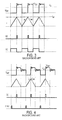
- FIG. 4 shows a timing diagram illustrating a conventional flyback switching regulator operating in DCM.
- a fixed frequency synchronization signal SYNC is supplied to turn on the switch of the DCM switching regulator, whereas the OC signal is used to turn off the switch.
- the secondary current i'sec is at a zero level much longer than in the BCM switching regulator described previously. Therefore, the BCM operation substantially reduces the ripple voltage at the output of the switch, and substantially reduces the resistive loss.
- FIG. 5 illustrates a known BCM control block 30 that provides minimum off-time control to reduce the "jittering" problem.
- the BCM control block 30 comprises a VC comparator 302 and an OC comparator 304 that generate the VC and OC signals in a manner similar to producing these signals in the BCM arrangement in FIG. 2 .
- the BCM control block 30 includes a fixed time delay circuit Min-OFF 306 that delays the OC signal and supplies the delayed signal to a first input of an AND gate circuit 308. A second input of the AND gate circuit 308 is fed with the VC signal.
- the output of the AND gate circuit 308 is supplied to the S-input of an RS flip-flop circuit 310 that produces a gate control signal at its Q-output.
- the Min-OFF delay circuit 306 delays the turning-on of the switch to set the minimum off-time period of the switch. If the switching off-time period is longer than the delay period, the delay circuit 306 has no effect on the switching.
- FIG. 6 illustrates another known way of reducing "jittering.”
- BCM control block 40 comprises a VC comparator 402 and an OC comparator 404 that generate the VC and OC signals in a manner similar to producing these signals in the BCM arrangement in FIG. 2 .
- the BCM control block 40 includes a MIN-Iref circuit 406 for setting a minimum value of the reference current Iref.
- the MIN-Iref circuit 406 may be a limiting circuit that prevents the reference current Iref from falling below a preset minimum value.
- the OC and VC signals are respectively supplied to the R- and S-inputs of the flip-flop circuit 410 that produces the gate control signal at its Q-output.
- the BCM control block 40 sets the minimum time period for the sensed current I to reach the reference value Iref. As a result, the minimum on-time period for the switching of the flyback switching regulator is established.
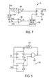
- FIG. 7 shows a conduction mode control arrangement that enables the flyback switching regulator 10 to operate alternatively in BCM or in DCM, combining advantages of these conductions modes, in accord with the teachings herein. Also, as discussed in more detail below, the conduction mode control arrangement in FIG. 7 enables the flyback switching regulator to operate in a hybrid BCM/DCM mode, in which the switching regulator operates in BCM at some predetermined conditions and operates in DCM at other predetermined conditions.
- a conduction mode control block 50 in FIG. 7 comprises a VC comparator 502 and an OC comparator 504 that respectively generate the described VC and OC signals using a subtraction circuit 506 and compensator Gc in a manner similar to production of these signals in the BCM arrangement in FIG. 2 .
- the conduction mode control block 50 receives an external synchronization signal SYNC having a programmable frequency f sync .
- the SYNC signal may be generated by an external pulse signal generator.
- the VC signal and the SYNC signal are supplied to a second pulse selector (SPS) 508 having its output coupled to an S-input of the flip-flop circuit 510 that produces a gate control signal at its Q-output.
- the gate control signal controls switching of the switch S ( FIG. 1 ) in the flyback switching regulator 10.
- the SPS 508 is configured to pass to its output only one or the other of the supplied input signals. In particular, only that input signal which is supplied later than the other input signal is allowed to pass to the output of the SPS 508.
- the SPS 508 may comprise RS flip-flop circuits 602 and 604, an AND gate circuit 606 and a delay circuit 608.
- the VC and SYNC signals are respectively supplied to S-inputs of the flip-flop circuits 602 and 604 to set output signals at their Q-ouputs.
- the output signals of the flip-flop circuits 602 and 604 are supplied to respective inputs of the AND gate circuit 606.
- the output signal of the AND gate 606 is delayed by the delay circuit 608 and supplied to R-inputs of the flip-flop circuits 602 and 604 to reset their output signals.
- the delay circuit 609 may delay the output signal of the AND gate 606 by about 100 ns.
- the SPS 508 passes the VC signal to set the gate control signal if the VC signal is produced after the SYNC signal is supplied, and passes the SYNC signal to set the gate control signal if the VC signal is produced before the SYNC signal is supplied. Further, when the SYNC signal is at a high level, the VC signal always passes to the input of the flip-flop circuit 510. However, when the SYNC signal is at a low level, the VC signal is prevented from passing to the input of the flip-flop circuit 510 to keep the switch S of the flyback switching regulator in an off-state.
- the conduction mode control block 50 uses control signals OC, VC and SYNC to control switching of the flyback switching regulator 10.
- the switch S is turned off by the OC signal when the sensed current I reaches the reference current value Iref.
- the flyback switching regulator 10 operates in BCM (dotted waveform of current I).
- BCM dotted waveform of current I
- the VC signal causes the switch S to turn on immediately after the current i'sec in the secondary winding falls to a zero level.
- the current in the transformer Tr is maintained at a non-zero level during time period T1 within each switching cycle of the switching regulator 10.
- the flyback switching regulator 10 operates in DCM (solid waveform of current I).
- DCM solid waveform of current I.
- the current in the transformer Tr remains at a zero level until the SYNC signal is supplied to turn on the switch S.
- the current in the transformer Tr is maintained at a non-zero level during time period T2 within each switching cycle of the switching regulator 10.
- the time period T1 differs from the time period T2.
- a desired conduction mode of the flyback switching regulator 10 may be set by programming the frequency f sync of the SYNC signal.
- the frequency f sync may be set higher than the expected maximum BCM frequency.
- the second pulse selector 508 selects the VC signal instead of the SYNC signal.
- the frequency f sync may be set lower than the expected minimum BCM frequency.
- the second pulse selector 508 selects the SYNC signal instead of the VC signal.
- the BCM frequency may correspond to the frequency of the VC signal.
- the frequency f sync may be selected in a range between the expected maximum BCM frequency and the expected minimum BCM frequency.
- the flyback switching regulator 10 may automatically switch between the BCM and DCM modes of operation depending on load and line conditions. For example, the flyback switching regulator 10 will operate in the BCM at a heavier load, and in the DCM at a lighter load.
- the flyback switching regulator 10 may be controlled to operate in any one of three conduction modes using the same control arrangement such as shown in FIG. 7 .
- the flyback switching regulator 10 may be set to operate in DCM for lower power applications or at light load, to operate in BCM for higher power applications or at full load, and to operate in the hybrid BCM/DCM mode for intermediate power applications or at variable load.
Landscapes
- Engineering & Computer Science (AREA)
- Power Engineering (AREA)
- Dc-Dc Converters (AREA)
- Electronic Switches (AREA)
Abstract
Description
- The subject matter of this disclosure relates to power supply circuits, and more particularly to circuitry and methodology for controlling conduction mode in a switching circuit, such as a regulator.
- Switching regulators usually operate in either a continuous conduction mode (CCM) for higher power applications, or in a discontinuous conduction mode (DCM) for lower power applications. For example, when a switching regulator operates in CCM, current in its inductive element is always above zero, whereas in a DCM switching regulator, current in the inductive element falls to zero during a time period within each switching cycle.
- To take full advantage of energy transfer efficiency, most flyback switching regulators operate in DCM where an inherent diode reverse recovery problem is absent and switches operate at zero current turn-on. Due to reduced device stresses, a DCM switching regulator is able to operate at a higher frequency, which results in a smaller transformer size and higher power density. However, DCM operation is associated with high resistive loss and high ripple voltage. To minimize these disadvantages while maintaining advantages of DCM operation, a switching regulator may be controlled to operate at the boundary between CCM and DCM, i.e. in a boundary conduction mode (BCM).
- The efficiency of a BCM regulator is higher than that of a DCM regulator. However, the difference in efficiency between these modes becomes much smaller at high line voltage conditions. In addition, BCM operation has some disadvantages. A BCM controller adjusts switching frequency according to load and line conditions. Load step change and line voltage variation affect the switching frequency directly. The resulting variable switching frequency may shift the noise spectrum out of an acceptable range of electromagnetic interference (EMI) and cause uncertainty for EMI filtering.
- Variable switching frequency also affects output voltage ripple. When the switching frequency is high, output voltage ripple is low. Conversely, when switching frequency is low, output voltage ripple is high.
- Another disadvantage is "jittering" at light load conditions, when the switching frequency can reach a very high level.
- DCM operation enables a switching regulator to alleviate the EMI and "jittering" problems and conveniently provide ripple filtering. Therefore, it would be desirable to provide a conduction mode control system that will allow a switching regulator to combine benefits of BCM and DCM by having a capability to operate in either mode, selectively. Also, it would be desirable to control a switching converter so as to support its operation in a hybrid DCM/BCM mode, in which the converter is able to switch between BCM and DCM, depending on specific conditions.
- In accordance with one aspect of the disclosure, a control system that controls a switching circuit having a switching element and an inductive element coupled to an output of the switching element, includes a switching control circuit that controls the switching element to operate the switching circuit in a first conduction mode of operation, such as a boundary conduction mode (BCM), in which current in the inductive element is maintained at a non-zero level during a first time period within each switching cycle. A conduction mode control circuit is configured for switching the switching circuit into a second conduction mode of operation, such as a discontinuous conduction mode (DCM), in which current in the inductive element is maintained at a non-zero level during a second time period within each switching cycle. The first time period differs from the second time period.
- Further, the mode control circuit may set the switching circuit into a third conduction mode, in which the switching circuit may operate in the first conduction mode at a first predetermined condition and to operate in the second conduction mode at a second predetermined condition. For example, in the third conduction mode, the switching circuit may be controlled to operate in BCM at a heavy load condition and to operate in DCM at a light load condition.
- The switching circuit may include a switching regulator, such as a flyback switching regulator. In the first and second conduction modes, the flyback switching regulator may be controlled to have current in its transformer at a non-zero level during first and second time periods, respectively, in each switching cycle. The first time period may differ from the second time period.
- In accordance with an embodiment of the disclosure, the mode control circuit is responsive to a mode control signal having a parameter, such as frequency, programmable to select between the first conduction mode and the second conduction mode. Also, the parameter of the mode control signal may be programmable to enable the switching circuit to operate in the third conduction mode combining the first conduction mode and the second conduction mode.
- The mode control circuit may include a signal selector for selecting between the mode control signal and a conduction mode support signal produced. The switching circuit may be controlled to operate in the first conduction mode when the frequency of the mode control signal is set to a value exceeding an expected maximum frequency of the conduction mode support signal. The second conduction mode may be set when the frequency of the mode control signal is less than an expected minimum frequency of the conduction mode support signal. The third conduction mode may be established when the frequency of the mode control signal is in a range between the expected minimum frequency and the expected maximum frequency of the conduction mode support signal.
- In accordance with another aspect of the disclosure, a power supply system may comprise a switching circuit, and a mode control circuit for controlling a conduction mode of the switching circuit. The control circuit may be responsive to a mode control signal having a parameter, such as frequency, programmable to enable the switching circuit to switch between the first conduction mode and the second conduction mode.
- In accordance with an embodiment of the disclosure, the mode control circuit may include a signal selector for selecting between the mode control signal and a conduction mode support signal supplied to the mode control circuit to operate the switching circuit in the first conduction mode.
- The mode control circuit may further include an output circuit responsive to the signal selector for providing a switch control signal for controlling the switching element.
- The signal selector may be configured for passing to the output circuit a selected one of the mode control signal and the conduction mode support signal, and preventing from passing to the output circuit a non-selected one of the mode control signal and the conduction mode support signal.
- In particular, the signal selector may be configured to pass the conduction mode support signal to the output circuit to operate the switching circuit in the first conduction mode if the signal selector receives the conduction mode support signal after receiving the mode control signal. The mode control signal may be passed to the output circuit to operate the switching circuit in the second conduction mode if the signal selector receives the mode control signal after receiving the conduction mode support signal.
- The signal selector may include first and second flip-flop circuits having respective set inputs supplied by the conduction mode support signal and the mode control signal, respectively.
- The signal selector may further include an output gate circuit responsive to respective outputs of the first and second flip-flop circuits and having an output connected to respective reset inputs of the first and second flip-flop circuits.
- In accordance with a method of the present invention, the following steps are carried out to control a switching circuit:
- supporting operation of the switching circuit in the first conduction mode, such as BCM, and
- providing a mode control signal having a parameter programmable to enable operation of the switching circuit in the second conduction mode, such as DCM.
- Also, the parameter of the mode control signal may be programmable to enable operation of the switching circuit in a third conduction mode combining the first conduction mode and the second conduction mode.
- For example, frequency of the mode control signal may be programmable to set a conduction mode of the switching circuit.
- The control method of the present disclosure may further comprise the step of selecting between the mode control signal and an additional control signal to provide control of the switching element.
- In particular, the switching circuit may be controlled to operate in the first conduction mode if the additional control signal is supplied after the mode control signal. The second conduction mode may be set if the additional control signal is supplied before the mode control signal.
- Additional advantages and aspects of the disclosure will become readily apparent to those skilled in the art from the following detailed description, wherein embodiments of the present disclosure are shown and described, simply by way of illustration of the best mode contemplated for practicing the present disclosure. As will be described, the disclosure is capable of other and different embodiments, and its several details are susceptible of modification in various obvious respects, all without departing from the spirit of the disclosure. Accordingly, the drawings and description are to be regarded as illustrative in nature, and not as limitative.
- The following detailed description of the embodiments of the present disclosure can best be understood when read in conjunction with the following drawings, in which the features are not necessarily drawn to scale but rather are drawn as to best illustrate the pertinent features, wherein:
-
FIG. 1 shows an embodiment of a flyback switching regulator used conventionally in DCM operation. -
FIG. 2 illustrates an exemplary embodiment of a BCM control block used for controlling a flyback switching regulator. -
FIG. 3 shows a timing diagram illustrating BCM operation of the flyback switching regulator ofFig 1 . -
FIG. 4 shows a timing diagram illustrating DCM operation of the flyback switching regulator. -
FIG. 5 illustrates minimum off-time control of the flyback switching regulator. -
FIG. 6 illustrates minimum on-time control of the flyback switching regulator. -
FIG. 7 shows an exemplary embodiment of a conduction mode control block for controlling the flyback switching regulator in accord with the present disclosure. -
FIG. 8 shows an exemplary embodiment of a second pulse selector in the conduction mode control block. -
FIG. 9 shows a timing diagram illustrating selection of a conduction mode for the flyback switching regulator in accord with the present disclosure. - The present disclosure will be made using the example of a system for controlling a flyback switching regulator. It will become apparent, however, that the concept of the disclosure is applicable to setting a conduction mode of any switching circuit.
-
FIG. 1 shows an exemplary No-Optoflyback switching regulator 10 having a switch S, a transformer Tr with primary and secondary windings wpr and wsec, andcontroller 12 that controls switching of the switch S in BCM operation. A sense resistor Rsense is coupled to the switch S to monitor current I at the output of the switch S. A capacitor C and a diode D are coupled to the secondary winding wsec. The flyback switching regular 10 may convert an input DC voltage Vin into one or more output DC voltages with very high power conversion efficiency. - Referring to
FIG. 2 , thecontroller 12 may include aBCM control block 20 for controlling BCM operation of theflyback switching regulator 10. For example, the BCM control block may include asubtraction circuit 202 that determines a difference between the input voltage Vin supplied to the switchingregulator 10 and a switching voltage Vsw produced at the output of the switch S. The output signal of thesubtraction circuit 202, which reflects the output voltage, is supplied to a compensator Gc that produces a reference current value Iref to regulate the output voltage to Vref. For example, the compensator Gc may be an error amplifier that produces an output current Iref in order to keep the output voltage regulated. - Further, the
BCM control block 20 may include an overcurrent (OC)comparator 204, a voltage collapse (VC)comparator 206, and an RS flip-flop circuit 208 coupled to outputs of thecomparators OC comparator 204 compares a sensed current I with the reference current value Iref to produce an overcurrent signal OC when the sensed current I reaches the reference current value Iref. For example, the sensed current I may be determined by monitoring a voltage across the sense resistor Rsense. - The
VC comparator 206 compares the input voltage Vin with the switch voltage Vsw to produce a voltage collapse signal VC when the switch voltage Vsw falls below the input voltage Vin. The VC signal is supplied to the S-input of the RS flip-flop circuit 208 to set a gate control signal at the Q-output of the RS flip-flop circuit 208. The OC signal is applied as a gate reset signal to the R-input of the RS flip-flop circuit 208 to reset the gate control signal at the Q-output. When the gate control signal is set, it turns on the switch S. When the gate control signal is reset, it turns off the switch S. - As illustrated in the timing diagram of
FIG. 3 , theBCM control block 20 detects collapse of the switch voltage Vsw, which indicates that the current i'sec flowing through the diode D in the secondary winding of the transformer Tr crosses a zero level. Immediately after detecting the switch voltage collapse, the VC signal is produced to turn on the switch S. When the sensed current I represented on the diagram by the current in the primary winding ipr reaches the Iref level, the OC signal (gate reset signal) is produced to turn off the switch S. - For comparison,
FIG. 4 shows a timing diagram illustrating a conventional flyback switching regulator operating in DCM. A fixed frequency synchronization signal SYNC is supplied to turn on the switch of the DCM switching regulator, whereas the OC signal is used to turn off the switch. In the DCM switching regulator, the secondary current i'sec is at a zero level much longer than in the BCM switching regulator described previously. Therefore, the BCM operation substantially reduces the ripple voltage at the output of the switch, and substantially reduces the resistive loss. - However, BCM operation may result in "jittering" at light load conditions, when the switching frequency can reach a very high level.
FIG. 5 illustrates a knownBCM control block 30 that provides minimum off-time control to reduce the "jittering" problem. TheBCM control block 30 comprises aVC comparator 302 and anOC comparator 304 that generate the VC and OC signals in a manner similar to producing these signals in the BCM arrangement inFIG. 2 . Further, theBCM control block 30 includes a fixed time delay circuit Min-OFF 306 that delays the OC signal and supplies the delayed signal to a first input of an ANDgate circuit 308. A second input of the ANDgate circuit 308 is fed with the VC signal. The output of the ANDgate circuit 308 is supplied to the S-input of an RS flip-flop circuit 310 that produces a gate control signal at its Q-output. The Min-OFF delay circuit 306 delays the turning-on of the switch to set the minimum off-time period of the switch. If the switching off-time period is longer than the delay period, thedelay circuit 306 has no effect on the switching. -
FIG. 6 illustrates another known way of reducing "jittering."BCM control block 40 comprises aVC comparator 402 and anOC comparator 404 that generate the VC and OC signals in a manner similar to producing these signals in the BCM arrangement inFIG. 2 . Further, theBCM control block 40 includes a MIN-Iref circuit 406 for setting a minimum value of the reference current Iref. For example, the MIN-Iref circuit 406 may be a limiting circuit that prevents the reference current Iref from falling below a preset minimum value. The OC and VC signals are respectively supplied to the R- and S-inputs of the flip-flop circuit 410 that produces the gate control signal at its Q-output. By setting a minimum value for the reference current Iref, theBCM control block 40 sets the minimum time period for the sensed current I to reach the reference value Iref. As a result, the minimum on-time period for the switching of the flyback switching regulator is established. - Although the BCM arrangements in
FIGS. 5 and 6 limit the switching frequency of a BCM converter to a certain range, the switching frequency remains variable. Therefore, the above-discussed disadvantages of BCM converters are reduced but not eliminated. -
FIG. 7 shows a conduction mode control arrangement that enables theflyback switching regulator 10 to operate alternatively in BCM or in DCM, combining advantages of these conductions modes, in accord with the teachings herein. Also, as discussed in more detail below, the conduction mode control arrangement inFIG. 7 enables the flyback switching regulator to operate in a hybrid BCM/DCM mode, in which the switching regulator operates in BCM at some predetermined conditions and operates in DCM at other predetermined conditions. - A conduction
mode control block 50 inFIG. 7 comprises aVC comparator 502 and anOC comparator 504 that respectively generate the described VC and OC signals using asubtraction circuit 506 and compensator Gc in a manner similar to production of these signals in the BCM arrangement inFIG. 2 . In addition, the conductionmode control block 50 receives an external synchronization signal SYNC having a programmable frequency fsync. For example, the SYNC signal may be generated by an external pulse signal generator. The VC signal and the SYNC signal are supplied to a second pulse selector (SPS) 508 having its output coupled to an S-input of the flip-flop circuit 510 that produces a gate control signal at its Q-output. The gate control signal controls switching of the switch S (FIG. 1 ) in theflyback switching regulator 10. - The
SPS 508 is configured to pass to its output only one or the other of the supplied input signals. In particular, only that input signal which is supplied later than the other input signal is allowed to pass to the output of theSPS 508. As shown in the exemplary embodiment inFIG. 8 , theSPS 508 may comprise RS flip-flop circuits gate circuit 606 and adelay circuit 608. The VC and SYNC signals are respectively supplied to S-inputs of the flip-flop circuits flop circuits gate circuit 606. The output signal of the ANDgate 606 is delayed by thedelay circuit 608 and supplied to R-inputs of the flip-flop circuits gate 606 by about 100 ns. - As the AND
gate circuit 606 produces its output signal only after the last input signal is supplied at its input, theSPS 508 passes the VC signal to set the gate control signal if the VC signal is produced after the SYNC signal is supplied, and passes the SYNC signal to set the gate control signal if the VC signal is produced before the SYNC signal is supplied. Further, when the SYNC signal is at a high level, the VC signal always passes to the input of the flip-flop circuit 510. However, when the SYNC signal is at a low level, the VC signal is prevented from passing to the input of the flip-flop circuit 510 to keep the switch S of the flyback switching regulator in an off-state. - As illustrated by the waveforms in
FIG. 9 , the conductionmode control block 50 uses control signals OC, VC and SYNC to control switching of theflyback switching regulator 10. The switch S is turned off by the OC signal when the sensed current I reaches the reference current value Iref. - If the SYNC signal is supplied before the VC signal is produced (dotted waveform of the VC signal), i.e. before the switch voltage Vsw falls below the Vin level, the VC signal is selected by the
SPS 508 to turn on the switch S by setting the gate control signal. Therefore, theflyback switching regulator 10 operates in BCM (dotted waveform of current I). During BCM operation, the VC signal causes the switch S to turn on immediately after the current i'sec in the secondary winding falls to a zero level. Hence, in BCM, the current in the transformer Tr is maintained at a non-zero level during time period T1 within each switching cycle of the switchingregulator 10. - If the SYNC signal is supplied after the VC signal is produced (solid waveform of the VC signal), i.e. after the switch voltage Vsw falls below the Vin level, the SYNC signal is selected by the
SPS 508 to turn on the switch S by setting the gate control signal. Therefore, theflyback switching regulator 10 operates in DCM (solid waveform of current I). During DCM operation, the current in the transformer Tr remains at a zero level until the SYNC signal is supplied to turn on the switch S. Hence, in DCM, the current in the transformer Tr is maintained at a non-zero level during time period T2 within each switching cycle of the switchingregulator 10. The time period T1 differs from the time period T2. - A desired conduction mode of the
flyback switching regulator 10 may be set by programming the frequency fsync of the SYNC signal. In particular, to set theflyback switching regulator 10 into the BCM, the frequency fsync may be set higher than the expected maximum BCM frequency. In this case, thesecond pulse selector 508 selects the VC signal instead of the SYNC signal. To operate theflyback switching regulator 10 in DCM, the frequency fsync may be set lower than the expected minimum BCM frequency. In this case, thesecond pulse selector 508 selects the SYNC signal instead of the VC signal. The BCM frequency may correspond to the frequency of the VC signal. - Further, to establish a hybrid BCM/DCM mode of operation, the frequency fsync may be selected in a range between the expected maximum BCM frequency and the expected minimum BCM frequency. In the hybrid BCM/DCM mode, the
flyback switching regulator 10 may automatically switch between the BCM and DCM modes of operation depending on load and line conditions. For example, theflyback switching regulator 10 will operate in the BCM at a heavier load, and in the DCM at a lighter load. - Accordingly, the
flyback switching regulator 10 may be controlled to operate in any one of three conduction modes using the same control arrangement such as shown inFIG. 7 . By selecting a respective frequency of the SYNC signal, theflyback switching regulator 10 may be set to operate in DCM for lower power applications or at light load, to operate in BCM for higher power applications or at full load, and to operate in the hybrid BCM/DCM mode for intermediate power applications or at variable load. - The foregoing description illustrates and describes aspects of the present invention. Additionally, the disclosure shows and describes only preferred embodiments, but as aforementioned, it is to be understood that the invention is capable of use in various other combinations, modifications, and environments and is capable of changes or modifications within the scope of the inventive concept as expressed herein, commensurate with the above teachings, and/or the skill or knowledge of the relevant art.
- The embodiments described hereinabove are further intended to explain best modes known of practicing the invention and to enable others skilled in the art to utilize the invention in such, or other, embodiments and with the various modifications required by the particular applications or uses of the invention.
- Accordingly, the description is not intended to limit the invention to the form disclosed herein. Also, it is intended that the appended claims be construed to include alternative embodiments.
Claims (36)
- A control system (50) for controlling a switching circuit (10) having a switching element (S) and an inductive element coupled to an output of the switching element (S), the system (50) comprising:a switching control circuit for controlling the switching element (S) to operate the switching circuit (10) in a first conduction mode of operation, in which current in the inductive element is maintained at a non-zero level during a first time period within each of successive switching cycles, anda conduction mode control circuit for switching the switching circuit (10) into a second conduction mode of operation, in which current in the inductive element is maintained at a non-zero level during a second time period within each of successive switching cycles, the first time period being different from the second time period.
- The system (50) of claim 1, wherein the first conduction mode of operation is a boundary conduction mode (BCM), and the second conduction mode of operation is a discontinuous conduction mode (DCM).
- The system (50) of claim 1, wherein the mode control circuit is configured for enabling the switching circuit (10) to operate in a third conduction mode.
- The system (50) of claim 3, wherein, in the third conduction mode, the switching circuit (10) is controlled to operate in the first conduction mode in response to a first predetermined condition and to operate in the second conduction mode in response to a second predetermined condition.
- The system (50) of claim 3, wherein, in the third conduction mode, the switching circuit (10) is controlled to operate in BCM in response to the first predetermined condition and to operate in DCM in response to the second predetermined condition.
- The system (50) of claim 3, wherein, in the third conduction mode, the switching circuit (10) is controlled to operate in BCM at a heavy load condition and to operate in DCM at a lower load condition.
- The system (50) of claim 1, wherein the switching circuit (10) includes a switching regulator.
- The system (50) of claim 1, wherein the switching circuit (10) includes a flyback switching regulator having a transformer (Tr).
- The system (50) of claim 8, wherein in the first conduction mode of operation, current in the transformer (Tr) is maintained at a non-zero level during the first time period within each switching cycle; and in the second conduction mode of operation, current in the transformer (Tr) is maintained at a non-zero level during the second time period within each switching cycle.
- The system (50) of claim 1, wherein the mode control circuit is responsive to a mode control signal having a parameter programmable to select between the first conduction mode and the second conduction mode.
- The system (50) of claim 10, wherein the parameter of the mode control signal is programmable to enable the switching circuit (10) to operate in a third conduction mode combining the first conduction mode and the second conduction mode.
- The system (50) of claim 1, wherein the mode control circuit is responsive to a mode control signal having a frequency programmable to select between the first conduction mode of operation and the second conduction mode of operation.
- The system (50) of claim 12, wherein the frequency of the mode control signal is programmable to enable the switching circuit (10) to operate in a third conduction mode of operation combining the first conduction mode of operation and the second conduction mode of operation.
- The system of claim 13, (50) wherein the mode control circuit includes a signal selector for selecting between the mode control signal and a conduction mode support signal produced by the switching control circuit.
- The system (50) of claim 13, wherein the switching circuit (10) is configured to be controlled to operate in the first conduction mode when the frequency of the mode control signal is set to a value exceeding an expected maximum frequency of the conduction mode support signal.
- The system (50) of claim 15, wherein the switching circuit (10) is configured to be controlled to operate in the second conduction mode when the frequency of the mode control signal is set to a value less than an expected minimum frequency of the conduction mode support signal.
- The system (50) of claim 16, wherein the switching circuit (10) is configured to be controlled to operate in the third conduction mode when the frequency of the mode control signal is set to a value in a range between the expected minimum frequency and the expected maximum frequency of the conduction mode support signal.
- A power supply system comprising:a switching circuit (10) having a switching element (S) and an inductive element coupled to an output of the switching element (S), anda mode control circuit for controlling a conduction mode of operation of the switching circuit (10), the control circuit being responsive to a mode control signal having a parameter programmable to enable the switching circuit (10) to switch between a first conduction mode of operation, in which current in the inductive element is maintained at a non-zero level during a first time period within each switching cycle, and a second conduction mode of operation, in which current in the inductive element is maintained at a non-zero level during a second time period within each switching cycle, the first time differs from the second time period.
- The system of claim 18, wherein the mode control circuit is configured for controlling the conduction mode in response to the mode control signal having programmable frequency.
- The system of claim 19, wherein the mode control circuit includes a signal selector (508) for selecting between the mode control signal and a conduction mode support signal supplied to the mode control circuit to operate the switching circuit (10) in the first conduction mode.
- The system of claim 20, wherein the mode control circuit further includes an output circuit (510) responsive to the signal selector (508) for providing a switch control signal for controlling the switching element (S).
- The system of claim 21, wherein the signal selector (508) is configured for passing to the output circuit (510) a selected one of the mode control signal and the conduction mode support signal, and preventing from passing to the output circuit (510) a non-selected one of the mode control signal and the conduction mode support signal.
- The system of claim 22, wherein the signal selector (508) is configured to pass the conduction mode support signal to the output circuit (510) to operate the switching circuit (10) in the first conduction mode if the signal selector (508) receives the conduction mode support signal after receiving the mode control signal.
- The system of claim 23, wherein the signal selector (508) is configured to pass the mode control signal to the output circuit (510) to operate the switching circuit in the second conduction mode if the signal selector (508) receives the mode control signal after receiving the conduction mode support signal.
- The system of claim 24, wherein the signal selector (508) includes first (602) and second (604) flip-flop circuits having respective set inputs supplied by the conduction mode support signal and the mode control signal respectively.
- The system of claim 25, wherein the signal selector (508) further includes an output gate circuit (606) responsive to respective outputs of the first (602) and second (604) flip-flop circuits and having an output connected to respective reset inputs of the first (602) and second (604) flip-flop circuits.
- The system of claim 18, wherein the switching circuit (10) includes a flyback switching regulator having a transformer (Tr).
- The system of claim 27, wherein in the first conduction mode of operation, current in the transformer (Tr) is maintained at a non-zero level during the first time period within each switching cycle; and in the second conduction mode of operation, current in the transformer (Tr) is maintained at a non-zero level during the second time period within each switching cycle.
- The system of claim 18, wherein the mode control circuit is configured to enable the switching circuit (10) to operate in BCM and DCM, alternatively, in response to prescribed conditions.
- A method of controlling a switching circuit (10) having a switching element (S) and an inductive element coupled to an output of the switching element (S), the method comprising the steps of:supporting operation of the switching circuit (10) in a first conduction mode, in which current in the inductive element is maintained at a non-zero level during a first time period within each switching cycle, andproviding a mode control signal having a parameter programmable to enable operation of the switching circuit (10) in a second conduction mode, in which current in the inductive element is maintained at a non-zero level during a second time period within each switching cycle, the first time period being different from the second time period.
- The method of claim 30, wherein the parameter of the mode control signal is programmable to enable operation of the switching circuit (10) in a third conduction mode combining the first conduction mode and the second conduction mode.
- The method of claim 31, wherein the first conduction mode is BCM, and the second conduction mode is DCM.
- The method of claim 31, wherein frequency of the mode control signal is programmable to set a conduction mode of the switching circuit (10).
- The method of claim 33, further comprising the step of selecting between the mode control signal and an additional control signal to provide control of the switching element (S).
- The method of claim 34, wherein the switching circuit (10) is controlled to operate in the first conduction mode if the additional control signal is supplied after the mode control signal.
- The method of claim 35, wherein the switching circuit (10) is controlled to operate in the second conduction mode if the additional control signal is supplied before the mode control signal.
Applications Claiming Priority (1)
| Application Number | Priority Date | Filing Date | Title |
|---|---|---|---|
| US11/605,297 US7733672B2 (en) | 2006-11-29 | 2006-11-29 | Programmable conduction mode control for switching circuits |
Publications (3)
| Publication Number | Publication Date |
|---|---|
| EP1928079A2 true EP1928079A2 (en) | 2008-06-04 |
| EP1928079A3 EP1928079A3 (en) | 2010-12-01 |
| EP1928079B1 EP1928079B1 (en) | 2014-01-15 |
Family
ID=39181827
Family Applications (1)
| Application Number | Title | Priority Date | Filing Date |
|---|---|---|---|
| EP07121449.8A Not-in-force EP1928079B1 (en) | 2006-11-29 | 2007-11-23 | Programmable conduction mode control for switching circuits |
Country Status (2)
| Country | Link |
|---|---|
| US (1) | US7733672B2 (en) |
| EP (1) | EP1928079B1 (en) |
Cited By (1)
| Publication number | Priority date | Publication date | Assignee | Title |
|---|---|---|---|---|
| CN102013798A (en) * | 2009-09-04 | 2011-04-13 | 立锜科技股份有限公司 | Switching power supply and driving circuit and control method thereof |
Families Citing this family (5)
| Publication number | Priority date | Publication date | Assignee | Title |
|---|---|---|---|---|
| NZ576387A (en) * | 2009-04-20 | 2011-06-30 | Eaton Ind Co | PFC booster circuit |
| US9484803B2 (en) | 2010-12-24 | 2016-11-01 | Semiconductor Components Industries, Llc | Method for regulating an output voltage |
| US10848051B2 (en) * | 2017-10-26 | 2020-11-24 | Analog Devices International Unlimited Company | Synchronizing hiccup over-current protection of multiphase switching converters |
| CN113472210B (en) * | 2021-07-05 | 2022-05-17 | 电子科技大学 | A hybrid control circuit for primary-side feedback flyback converter |
| TWI822546B (en) * | 2022-06-01 | 2023-11-11 | 立錡科技股份有限公司 | Switched capacitor voltage converter circuit and control method of switched capacitor converter |
Family Cites Families (6)
| Publication number | Priority date | Publication date | Assignee | Title |
|---|---|---|---|---|
| US6469917B1 (en) * | 2001-08-16 | 2002-10-22 | Green Power Technologies Ltd. | PFC apparatus for a converter operating in the borderline conduction mode |
| US6728117B2 (en) * | 2001-10-23 | 2004-04-27 | Koninklijke Philips Electronics N.V. | Frequency modulated self-oscillating switching power supply |
| FR2848356A1 (en) * | 2002-12-05 | 2004-06-11 | St Microelectronics Sa | METHOD FOR CONTROLLING A POWER SUPPLY WITH A SINGLE INDUCTIVE ELEMENT AND MULTIPLE OUTPUTS, AND CORRESPONDING POWER SUPPLY, PARTICULARLY FOR A CELLULAR MOBILE TELEPHONE |
| US7045992B1 (en) * | 2004-06-22 | 2006-05-16 | National Semiconductor Corporation | Apparatus and method for start-up for a synchronous switching regulator |
| US7288924B2 (en) * | 2004-07-16 | 2007-10-30 | Cellex Power Products, Inc. | Digital input current control for switch mode power supplies |
| US7855864B2 (en) * | 2005-03-31 | 2010-12-21 | Semtech Corporation | Switched mode power supply method and apparatus |
-
2006
- 2006-11-29 US US11/605,297 patent/US7733672B2/en active Active
-
2007
- 2007-11-23 EP EP07121449.8A patent/EP1928079B1/en not_active Not-in-force
Non-Patent Citations (1)
| Title |
|---|
| None |
Cited By (2)
| Publication number | Priority date | Publication date | Assignee | Title |
|---|---|---|---|---|
| CN102013798A (en) * | 2009-09-04 | 2011-04-13 | 立锜科技股份有限公司 | Switching power supply and driving circuit and control method thereof |
| CN102013798B (en) * | 2009-09-04 | 2014-03-26 | 立锜科技股份有限公司 | Switching power supply and its drive circuit and control method |
Also Published As
| Publication number | Publication date |
|---|---|
| US20080122420A1 (en) | 2008-05-29 |
| EP1928079B1 (en) | 2014-01-15 |
| EP1928079A3 (en) | 2010-12-01 |
| US7733672B2 (en) | 2010-06-08 |
Similar Documents
| Publication | Publication Date | Title |
|---|---|---|
| US9093909B2 (en) | Switching mode power supply and the method thereof | |
| JP5509182B2 (en) | Method and apparatus for limiting output power in a switching power supply | |
| US5532577A (en) | Method and apparatus for multiple output regulation in a step-down switching regulator | |
| JP4856415B2 (en) | Method and apparatus for providing temporary peak power from a switching regulator | |
| US9444364B2 (en) | Adaptive peak power control | |
| US7826237B2 (en) | Method and system for efficient power control with multiple modes | |
| US7045992B1 (en) | Apparatus and method for start-up for a synchronous switching regulator | |
| US20030128018A1 (en) | Methods for regulation of power converters using primary-only feedback | |
| US8891259B2 (en) | Control circuit and method for audible noise suppression in a power converter | |
| US20130027996A1 (en) | Variable frequency timing circuit for a power supply control circuit | |
| US9680383B2 (en) | Input overvoltage protection using current limit | |
| EP1928079B1 (en) | Programmable conduction mode control for switching circuits | |
| JP2017017767A (en) | High efficiency power factor improvement circuit and switching power supply device | |
| WO2015105601A1 (en) | Circuits and techniques for improving regulation in a regulator having more than one mode of operation | |
| US10797591B2 (en) | Power controllers with frequency jittering, and control methods thereof | |
| KR101919625B1 (en) | Current controlling mode DC-DC Converter | |
| JP5974563B2 (en) | Step-up switching power supply | |
| US11996778B2 (en) | Circuit for controlling a switching mode power supply and the method thereof | |
| US11063520B2 (en) | Simplified hybrid PWM/PFM control method for SLLC converter | |
| US20160056722A1 (en) | Dc-dc converter | |
| WO2007005183A2 (en) | Switching power supply control with phase shift | |
| JP2009153373A (en) | Power supply control circuit and power supply control method | |
| US8988055B2 (en) | Digital windowing current-mode controller for a DC-DC converter | |
| JP2020065402A (en) | Switching regulator | |
| CN100492839C (en) | DC-DC converter and its controller and control method and device containing same |
Legal Events
| Date | Code | Title | Description |
|---|---|---|---|
| PUAI | Public reference made under article 153(3) epc to a published international application that has entered the european phase |
Free format text: ORIGINAL CODE: 0009012 |
|
| AK | Designated contracting states |
Kind code of ref document: A2 Designated state(s): AT BE BG CH CY CZ DE DK EE ES FI FR GB GR HU IE IS IT LI LT LU LV MC MT NL PL PT RO SE SI SK TR |
|
| AX | Request for extension of the european patent |
Extension state: AL BA HR MK RS |
|
| PUAL | Search report despatched |
Free format text: ORIGINAL CODE: 0009013 |
|
| AK | Designated contracting states |
Kind code of ref document: A3 Designated state(s): AT BE BG CH CY CZ DE DK EE ES FI FR GB GR HU IE IS IT LI LT LU LV MC MT NL PL PT RO SE SI SK TR |
|
| AX | Request for extension of the european patent |
Extension state: AL BA HR MK RS |
|
| 17P | Request for examination filed |
Effective date: 20110601 |
|
| AKX | Designation fees paid |
Designated state(s): AT BE BG CH CY CZ DE DK EE ES FI FR GB GR HU IE IS IT LI LT LU LV MC MT NL PL PT RO SE SI SK TR |
|
| 17Q | First examination report despatched |
Effective date: 20110816 |
|
| RAP1 | Party data changed (applicant data changed or rights of an application transferred) |
Owner name: LINEAR TECHNOLOGY CORPORATION |
|
| GRAP | Despatch of communication of intention to grant a patent |
Free format text: ORIGINAL CODE: EPIDOSNIGR1 |
|
| INTG | Intention to grant announced |
Effective date: 20130828 |
|
| GRAS | Grant fee paid |
Free format text: ORIGINAL CODE: EPIDOSNIGR3 |
|
| GRAA | (expected) grant |
Free format text: ORIGINAL CODE: 0009210 |
|
| AK | Designated contracting states |
Kind code of ref document: B1 Designated state(s): AT BE BG CH CY CZ DE DK EE ES FI FR GB GR HU IE IS IT LI LT LU LV MC MT NL PL PT RO SE SI SK TR |
|
| REG | Reference to a national code |
Ref country code: GB Ref legal event code: FG4D Ref country code: CH Ref legal event code: EP |
|
| REG | Reference to a national code |
Ref country code: AT Ref legal event code: REF Ref document number: 650193 Country of ref document: AT Kind code of ref document: T Effective date: 20140215 |
|
| REG | Reference to a national code |
Ref country code: IE Ref legal event code: FG4D |
|
| REG | Reference to a national code |
Ref country code: DE Ref legal event code: R096 Ref document number: 602007034772 Country of ref document: DE Effective date: 20140227 |
|
| REG | Reference to a national code |
Ref country code: NL Ref legal event code: T3 |
|
| REG | Reference to a national code |
Ref country code: AT Ref legal event code: MK05 Ref document number: 650193 Country of ref document: AT Kind code of ref document: T Effective date: 20140115 |
|
| REG | Reference to a national code |
Ref country code: LT Ref legal event code: MG4D |
|
| PG25 | Lapsed in a contracting state [announced via postgrant information from national office to epo] |
Ref country code: LT Free format text: LAPSE BECAUSE OF FAILURE TO SUBMIT A TRANSLATION OF THE DESCRIPTION OR TO PAY THE FEE WITHIN THE PRESCRIBED TIME-LIMIT Effective date: 20140115 Ref country code: IS Free format text: LAPSE BECAUSE OF FAILURE TO SUBMIT A TRANSLATION OF THE DESCRIPTION OR TO PAY THE FEE WITHIN THE PRESCRIBED TIME-LIMIT Effective date: 20140515 |
|
| PG25 | Lapsed in a contracting state [announced via postgrant information from national office to epo] |
Ref country code: AT Free format text: LAPSE BECAUSE OF FAILURE TO SUBMIT A TRANSLATION OF THE DESCRIPTION OR TO PAY THE FEE WITHIN THE PRESCRIBED TIME-LIMIT Effective date: 20140115 Ref country code: SE Free format text: LAPSE BECAUSE OF FAILURE TO SUBMIT A TRANSLATION OF THE DESCRIPTION OR TO PAY THE FEE WITHIN THE PRESCRIBED TIME-LIMIT Effective date: 20140115 Ref country code: FI Free format text: LAPSE BECAUSE OF FAILURE TO SUBMIT A TRANSLATION OF THE DESCRIPTION OR TO PAY THE FEE WITHIN THE PRESCRIBED TIME-LIMIT Effective date: 20140115 Ref country code: PT Free format text: LAPSE BECAUSE OF FAILURE TO SUBMIT A TRANSLATION OF THE DESCRIPTION OR TO PAY THE FEE WITHIN THE PRESCRIBED TIME-LIMIT Effective date: 20140515 Ref country code: CY Free format text: LAPSE BECAUSE OF FAILURE TO SUBMIT A TRANSLATION OF THE DESCRIPTION OR TO PAY THE FEE WITHIN THE PRESCRIBED TIME-LIMIT Effective date: 20140115 Ref country code: ES Free format text: LAPSE BECAUSE OF FAILURE TO SUBMIT A TRANSLATION OF THE DESCRIPTION OR TO PAY THE FEE WITHIN THE PRESCRIBED TIME-LIMIT Effective date: 20140115 |
|
| PG25 | Lapsed in a contracting state [announced via postgrant information from national office to epo] |
Ref country code: BE Free format text: LAPSE BECAUSE OF FAILURE TO SUBMIT A TRANSLATION OF THE DESCRIPTION OR TO PAY THE FEE WITHIN THE PRESCRIBED TIME-LIMIT Effective date: 20140115 Ref country code: LV Free format text: LAPSE BECAUSE OF FAILURE TO SUBMIT A TRANSLATION OF THE DESCRIPTION OR TO PAY THE FEE WITHIN THE PRESCRIBED TIME-LIMIT Effective date: 20140115 |
|
| REG | Reference to a national code |
Ref country code: DE Ref legal event code: R097 Ref document number: 602007034772 Country of ref document: DE |
|
| PG25 | Lapsed in a contracting state [announced via postgrant information from national office to epo] |
Ref country code: EE Free format text: LAPSE BECAUSE OF FAILURE TO SUBMIT A TRANSLATION OF THE DESCRIPTION OR TO PAY THE FEE WITHIN THE PRESCRIBED TIME-LIMIT Effective date: 20140115 Ref country code: RO Free format text: LAPSE BECAUSE OF FAILURE TO SUBMIT A TRANSLATION OF THE DESCRIPTION OR TO PAY THE FEE WITHIN THE PRESCRIBED TIME-LIMIT Effective date: 20140115 Ref country code: CZ Free format text: LAPSE BECAUSE OF FAILURE TO SUBMIT A TRANSLATION OF THE DESCRIPTION OR TO PAY THE FEE WITHIN THE PRESCRIBED TIME-LIMIT Effective date: 20140115 Ref country code: DK Free format text: LAPSE BECAUSE OF FAILURE TO SUBMIT A TRANSLATION OF THE DESCRIPTION OR TO PAY THE FEE WITHIN THE PRESCRIBED TIME-LIMIT Effective date: 20140115 |
|
| PLBE | No opposition filed within time limit |
Free format text: ORIGINAL CODE: 0009261 |
|
| STAA | Information on the status of an ep patent application or granted ep patent |
Free format text: STATUS: NO OPPOSITION FILED WITHIN TIME LIMIT |
|
| PG25 | Lapsed in a contracting state [announced via postgrant information from national office to epo] |
Ref country code: SK Free format text: LAPSE BECAUSE OF FAILURE TO SUBMIT A TRANSLATION OF THE DESCRIPTION OR TO PAY THE FEE WITHIN THE PRESCRIBED TIME-LIMIT Effective date: 20140115 Ref country code: PL Free format text: LAPSE BECAUSE OF FAILURE TO SUBMIT A TRANSLATION OF THE DESCRIPTION OR TO PAY THE FEE WITHIN THE PRESCRIBED TIME-LIMIT Effective date: 20140115 |
|
| 26N | No opposition filed |
Effective date: 20141016 |
|
| REG | Reference to a national code |
Ref country code: DE Ref legal event code: R097 Ref document number: 602007034772 Country of ref document: DE Effective date: 20141016 |
|
| PG25 | Lapsed in a contracting state [announced via postgrant information from national office to epo] |
Ref country code: SI Free format text: LAPSE BECAUSE OF FAILURE TO SUBMIT A TRANSLATION OF THE DESCRIPTION OR TO PAY THE FEE WITHIN THE PRESCRIBED TIME-LIMIT Effective date: 20140115 |
|
| PG25 | Lapsed in a contracting state [announced via postgrant information from national office to epo] |
Ref country code: MC Free format text: LAPSE BECAUSE OF FAILURE TO SUBMIT A TRANSLATION OF THE DESCRIPTION OR TO PAY THE FEE WITHIN THE PRESCRIBED TIME-LIMIT Effective date: 20140115 Ref country code: LU Free format text: LAPSE BECAUSE OF FAILURE TO SUBMIT A TRANSLATION OF THE DESCRIPTION OR TO PAY THE FEE WITHIN THE PRESCRIBED TIME-LIMIT Effective date: 20141123 |
|
| REG | Reference to a national code |
Ref country code: CH Ref legal event code: PL |
|
| PG25 | Lapsed in a contracting state [announced via postgrant information from national office to epo] |
Ref country code: LI Free format text: LAPSE BECAUSE OF NON-PAYMENT OF DUE FEES Effective date: 20141130 Ref country code: CH Free format text: LAPSE BECAUSE OF NON-PAYMENT OF DUE FEES Effective date: 20141130 |
|
| REG | Reference to a national code |
Ref country code: IE Ref legal event code: MM4A |
|
| PG25 | Lapsed in a contracting state [announced via postgrant information from national office to epo] |
Ref country code: IE Free format text: LAPSE BECAUSE OF NON-PAYMENT OF DUE FEES Effective date: 20141123 |
|
| REG | Reference to a national code |
Ref country code: FR Ref legal event code: PLFP Year of fee payment: 9 |
|
| PG25 | Lapsed in a contracting state [announced via postgrant information from national office to epo] |
Ref country code: BG Free format text: LAPSE BECAUSE OF FAILURE TO SUBMIT A TRANSLATION OF THE DESCRIPTION OR TO PAY THE FEE WITHIN THE PRESCRIBED TIME-LIMIT Effective date: 20140115 |
|
| PG25 | Lapsed in a contracting state [announced via postgrant information from national office to epo] |
Ref country code: GR Free format text: LAPSE BECAUSE OF FAILURE TO SUBMIT A TRANSLATION OF THE DESCRIPTION OR TO PAY THE FEE WITHIN THE PRESCRIBED TIME-LIMIT Effective date: 20140416 |
|
| PG25 | Lapsed in a contracting state [announced via postgrant information from national office to epo] |
Ref country code: MT Free format text: LAPSE BECAUSE OF FAILURE TO SUBMIT A TRANSLATION OF THE DESCRIPTION OR TO PAY THE FEE WITHIN THE PRESCRIBED TIME-LIMIT Effective date: 20140115 Ref country code: TR Free format text: LAPSE BECAUSE OF FAILURE TO SUBMIT A TRANSLATION OF THE DESCRIPTION OR TO PAY THE FEE WITHIN THE PRESCRIBED TIME-LIMIT Effective date: 20140115 Ref country code: HU Free format text: LAPSE BECAUSE OF FAILURE TO SUBMIT A TRANSLATION OF THE DESCRIPTION OR TO PAY THE FEE WITHIN THE PRESCRIBED TIME-LIMIT; INVALID AB INITIO Effective date: 20071123 |
|
| REG | Reference to a national code |
Ref country code: FR Ref legal event code: PLFP Year of fee payment: 10 |
|
| REG | Reference to a national code |
Ref country code: FR Ref legal event code: PLFP Year of fee payment: 11 |
|
| REG | Reference to a national code |
Ref country code: FR Ref legal event code: PLFP Year of fee payment: 12 |
|
| REG | Reference to a national code |
Ref country code: DE Ref legal event code: R082 Ref document number: 602007034772 Country of ref document: DE Representative=s name: MUELLER-BORE & PARTNER PATENTANWAELTE PARTG MB, DE Ref country code: DE Ref legal event code: R081 Ref document number: 602007034772 Country of ref document: DE Owner name: ANALOG DEVICES INTERNATIONAL UNLIMITED COMPANY, IE Free format text: FORMER OWNER: LINEAR TECHNOLOGY CORP., MILPITAS, CALIF., US Ref country code: DE Ref legal event code: R082 Ref document number: 602007034772 Country of ref document: DE Representative=s name: WITHERS & ROGERS LLP, DE |
|
| REG | Reference to a national code |
Ref country code: DE Ref legal event code: R082 Ref document number: 602007034772 Country of ref document: DE Representative=s name: WITHERS & ROGERS LLP, DE |
|
| REG | Reference to a national code |
Ref country code: GB Ref legal event code: 732E Free format text: REGISTERED BETWEEN 20210930 AND 20211006 |
|
| PGFP | Annual fee paid to national office [announced via postgrant information from national office to epo] |
Ref country code: NL Payment date: 20211020 Year of fee payment: 15 |
|
| REG | Reference to a national code |
Ref country code: NL Ref legal event code: PD Owner name: ANALOG DEVICES INTERNATIONAL UNLIMITED COMPANY; IE Free format text: DETAILS ASSIGNMENT: CHANGE OF OWNER(S), ASSIGNMENT; FORMER OWNER NAME: LINEAR TECHNOLOGY LLC Effective date: 20211216 |
|
| PGFP | Annual fee paid to national office [announced via postgrant information from national office to epo] |
Ref country code: GB Payment date: 20211020 Year of fee payment: 15 |
|
| PGFP | Annual fee paid to national office [announced via postgrant information from national office to epo] |
Ref country code: IT Payment date: 20211025 Year of fee payment: 15 Ref country code: FR Payment date: 20211020 Year of fee payment: 15 |
|
| PGFP | Annual fee paid to national office [announced via postgrant information from national office to epo] |
Ref country code: DE Payment date: 20220616 Year of fee payment: 16 |
|
| REG | Reference to a national code |
Ref country code: NL Ref legal event code: MM Effective date: 20221201 |
|
| GBPC | Gb: european patent ceased through non-payment of renewal fee |
Effective date: 20221123 |
|
| PG25 | Lapsed in a contracting state [announced via postgrant information from national office to epo] |
Ref country code: NL Free format text: LAPSE BECAUSE OF NON-PAYMENT OF DUE FEES Effective date: 20221201 |
|
| PG25 | Lapsed in a contracting state [announced via postgrant information from national office to epo] |
Ref country code: IT Free format text: LAPSE BECAUSE OF NON-PAYMENT OF DUE FEES Effective date: 20221123 Ref country code: GB Free format text: LAPSE BECAUSE OF NON-PAYMENT OF DUE FEES Effective date: 20221123 |
|
| PG25 | Lapsed in a contracting state [announced via postgrant information from national office to epo] |
Ref country code: FR Free format text: LAPSE BECAUSE OF NON-PAYMENT OF DUE FEES Effective date: 20221130 |
|
| REG | Reference to a national code |
Ref country code: DE Ref legal event code: R119 Ref document number: 602007034772 Country of ref document: DE |
|
| PG25 | Lapsed in a contracting state [announced via postgrant information from national office to epo] |
Ref country code: DE Free format text: LAPSE BECAUSE OF NON-PAYMENT OF DUE FEES Effective date: 20240601 |
|
| PG25 | Lapsed in a contracting state [announced via postgrant information from national office to epo] |
Ref country code: DE Free format text: LAPSE BECAUSE OF NON-PAYMENT OF DUE FEES Effective date: 20240601 |