EP1925968A2 - Liquid crystal device and electronic apparatus - Google Patents
Liquid crystal device and electronic apparatus Download PDFInfo
- Publication number
- EP1925968A2 EP1925968A2 EP07022369A EP07022369A EP1925968A2 EP 1925968 A2 EP1925968 A2 EP 1925968A2 EP 07022369 A EP07022369 A EP 07022369A EP 07022369 A EP07022369 A EP 07022369A EP 1925968 A2 EP1925968 A2 EP 1925968A2
- Authority
- EP
- European Patent Office
- Prior art keywords
- liquid crystal
- substrate
- crystal layer
- polarizing plate
- crystal device
- Prior art date
- Legal status (The legal status is an assumption and is not a legal conclusion. Google has not performed a legal analysis and makes no representation as to the accuracy of the status listed.)
- Withdrawn
Links
Images





Classifications
-
- G—PHYSICS
- G02—OPTICS
- G02F—OPTICAL DEVICES OR ARRANGEMENTS FOR THE CONTROL OF LIGHT BY MODIFICATION OF THE OPTICAL PROPERTIES OF THE MEDIA OF THE ELEMENTS INVOLVED THEREIN; NON-LINEAR OPTICS; FREQUENCY-CHANGING OF LIGHT; OPTICAL LOGIC ELEMENTS; OPTICAL ANALOGUE/DIGITAL CONVERTERS
- G02F1/00—Devices or arrangements for the control of the intensity, colour, phase, polarisation or direction of light arriving from an independent light source, e.g. switching, gating or modulating; Non-linear optics
- G02F1/01—Devices or arrangements for the control of the intensity, colour, phase, polarisation or direction of light arriving from an independent light source, e.g. switching, gating or modulating; Non-linear optics for the control of the intensity, phase, polarisation or colour
- G02F1/13—Devices or arrangements for the control of the intensity, colour, phase, polarisation or direction of light arriving from an independent light source, e.g. switching, gating or modulating; Non-linear optics for the control of the intensity, phase, polarisation or colour based on liquid crystals, e.g. single liquid crystal display cells
- G02F1/133—Constructional arrangements; Operation of liquid crystal cells; Circuit arrangements
- G02F1/1333—Constructional arrangements; Manufacturing methods
- G02F1/1335—Structural association of cells with optical devices, e.g. polarisers or reflectors
- G02F1/133528—Polarisers
-
- G—PHYSICS
- G02—OPTICS
- G02F—OPTICAL DEVICES OR ARRANGEMENTS FOR THE CONTROL OF LIGHT BY MODIFICATION OF THE OPTICAL PROPERTIES OF THE MEDIA OF THE ELEMENTS INVOLVED THEREIN; NON-LINEAR OPTICS; FREQUENCY-CHANGING OF LIGHT; OPTICAL LOGIC ELEMENTS; OPTICAL ANALOGUE/DIGITAL CONVERTERS
- G02F1/00—Devices or arrangements for the control of the intensity, colour, phase, polarisation or direction of light arriving from an independent light source, e.g. switching, gating or modulating; Non-linear optics
- G02F1/01—Devices or arrangements for the control of the intensity, colour, phase, polarisation or direction of light arriving from an independent light source, e.g. switching, gating or modulating; Non-linear optics for the control of the intensity, phase, polarisation or colour
- G02F1/13—Devices or arrangements for the control of the intensity, colour, phase, polarisation or direction of light arriving from an independent light source, e.g. switching, gating or modulating; Non-linear optics for the control of the intensity, phase, polarisation or colour based on liquid crystals, e.g. single liquid crystal display cells
- G02F1/133—Constructional arrangements; Operation of liquid crystal cells; Circuit arrangements
- G02F1/1333—Constructional arrangements; Manufacturing methods
- G02F1/1337—Surface-induced orientation of the liquid crystal molecules, e.g. by alignment layers
-
- G—PHYSICS
- G02—OPTICS
- G02F—OPTICAL DEVICES OR ARRANGEMENTS FOR THE CONTROL OF LIGHT BY MODIFICATION OF THE OPTICAL PROPERTIES OF THE MEDIA OF THE ELEMENTS INVOLVED THEREIN; NON-LINEAR OPTICS; FREQUENCY-CHANGING OF LIGHT; OPTICAL LOGIC ELEMENTS; OPTICAL ANALOGUE/DIGITAL CONVERTERS
- G02F1/00—Devices or arrangements for the control of the intensity, colour, phase, polarisation or direction of light arriving from an independent light source, e.g. switching, gating or modulating; Non-linear optics
- G02F1/01—Devices or arrangements for the control of the intensity, colour, phase, polarisation or direction of light arriving from an independent light source, e.g. switching, gating or modulating; Non-linear optics for the control of the intensity, phase, polarisation or colour
- G02F1/13—Devices or arrangements for the control of the intensity, colour, phase, polarisation or direction of light arriving from an independent light source, e.g. switching, gating or modulating; Non-linear optics for the control of the intensity, phase, polarisation or colour based on liquid crystals, e.g. single liquid crystal display cells
- G02F1/133—Constructional arrangements; Operation of liquid crystal cells; Circuit arrangements
- G02F1/1333—Constructional arrangements; Manufacturing methods
- G02F1/1335—Structural association of cells with optical devices, e.g. polarisers or reflectors
-
- G—PHYSICS
- G02—OPTICS
- G02F—OPTICAL DEVICES OR ARRANGEMENTS FOR THE CONTROL OF LIGHT BY MODIFICATION OF THE OPTICAL PROPERTIES OF THE MEDIA OF THE ELEMENTS INVOLVED THEREIN; NON-LINEAR OPTICS; FREQUENCY-CHANGING OF LIGHT; OPTICAL LOGIC ELEMENTS; OPTICAL ANALOGUE/DIGITAL CONVERTERS
- G02F1/00—Devices or arrangements for the control of the intensity, colour, phase, polarisation or direction of light arriving from an independent light source, e.g. switching, gating or modulating; Non-linear optics
- G02F1/01—Devices or arrangements for the control of the intensity, colour, phase, polarisation or direction of light arriving from an independent light source, e.g. switching, gating or modulating; Non-linear optics for the control of the intensity, phase, polarisation or colour
- G02F1/13—Devices or arrangements for the control of the intensity, colour, phase, polarisation or direction of light arriving from an independent light source, e.g. switching, gating or modulating; Non-linear optics for the control of the intensity, phase, polarisation or colour based on liquid crystals, e.g. single liquid crystal display cells
- G02F1/133—Constructional arrangements; Operation of liquid crystal cells; Circuit arrangements
- G02F1/1333—Constructional arrangements; Manufacturing methods
- G02F1/1335—Structural association of cells with optical devices, e.g. polarisers or reflectors
- G02F1/133528—Polarisers
- G02F1/133531—Polarisers characterised by the arrangement of polariser or analyser axes
-
- G—PHYSICS
- G02—OPTICS
- G02F—OPTICAL DEVICES OR ARRANGEMENTS FOR THE CONTROL OF LIGHT BY MODIFICATION OF THE OPTICAL PROPERTIES OF THE MEDIA OF THE ELEMENTS INVOLVED THEREIN; NON-LINEAR OPTICS; FREQUENCY-CHANGING OF LIGHT; OPTICAL LOGIC ELEMENTS; OPTICAL ANALOGUE/DIGITAL CONVERTERS
- G02F1/00—Devices or arrangements for the control of the intensity, colour, phase, polarisation or direction of light arriving from an independent light source, e.g. switching, gating or modulating; Non-linear optics
- G02F1/01—Devices or arrangements for the control of the intensity, colour, phase, polarisation or direction of light arriving from an independent light source, e.g. switching, gating or modulating; Non-linear optics for the control of the intensity, phase, polarisation or colour
- G02F1/13—Devices or arrangements for the control of the intensity, colour, phase, polarisation or direction of light arriving from an independent light source, e.g. switching, gating or modulating; Non-linear optics for the control of the intensity, phase, polarisation or colour based on liquid crystals, e.g. single liquid crystal display cells
- G02F1/137—Devices or arrangements for the control of the intensity, colour, phase, polarisation or direction of light arriving from an independent light source, e.g. switching, gating or modulating; Non-linear optics for the control of the intensity, phase, polarisation or colour based on liquid crystals, e.g. single liquid crystal display cells characterised by the electro-optical or magneto-optical effect, e.g. field-induced phase transition, orientation effect, guest-host interaction or dynamic scattering
- G02F1/139—Devices or arrangements for the control of the intensity, colour, phase, polarisation or direction of light arriving from an independent light source, e.g. switching, gating or modulating; Non-linear optics for the control of the intensity, phase, polarisation or colour based on liquid crystals, e.g. single liquid crystal display cells characterised by the electro-optical or magneto-optical effect, e.g. field-induced phase transition, orientation effect, guest-host interaction or dynamic scattering based on orientation effects in which the liquid crystal remains transparent
- G02F1/1396—Devices or arrangements for the control of the intensity, colour, phase, polarisation or direction of light arriving from an independent light source, e.g. switching, gating or modulating; Non-linear optics for the control of the intensity, phase, polarisation or colour based on liquid crystals, e.g. single liquid crystal display cells characterised by the electro-optical or magneto-optical effect, e.g. field-induced phase transition, orientation effect, guest-host interaction or dynamic scattering based on orientation effects in which the liquid crystal remains transparent the liquid crystal being selectively controlled between a twisted state and a non-twisted state, e.g. TN-LC cell
-
- G—PHYSICS
- G02—OPTICS
- G02F—OPTICAL DEVICES OR ARRANGEMENTS FOR THE CONTROL OF LIGHT BY MODIFICATION OF THE OPTICAL PROPERTIES OF THE MEDIA OF THE ELEMENTS INVOLVED THEREIN; NON-LINEAR OPTICS; FREQUENCY-CHANGING OF LIGHT; OPTICAL LOGIC ELEMENTS; OPTICAL ANALOGUE/DIGITAL CONVERTERS
- G02F2413/00—Indexing scheme related to G02F1/13363, i.e. to birefringent elements, e.g. for optical compensation, characterised by the number, position, orientation or value of the compensation plates
- G02F2413/10—Indexing scheme related to G02F1/13363, i.e. to birefringent elements, e.g. for optical compensation, characterised by the number, position, orientation or value of the compensation plates with refractive index ellipsoid inclined, or tilted, relative to the LC-layer surface O plate
- G02F2413/105—Indexing scheme related to G02F1/13363, i.e. to birefringent elements, e.g. for optical compensation, characterised by the number, position, orientation or value of the compensation plates with refractive index ellipsoid inclined, or tilted, relative to the LC-layer surface O plate with varying inclination in thickness direction, e.g. hybrid oriented discotic LC
-
- H—ELECTRICITY
- H04—ELECTRIC COMMUNICATION TECHNIQUE
- H04N—PICTORIAL COMMUNICATION, e.g. TELEVISION
- H04N13/00—Stereoscopic video systems; Multi-view video systems; Details thereof
- H04N13/30—Image reproducers
- H04N13/302—Image reproducers for viewing without the aid of special glasses, i.e. using autostereoscopic displays
- H04N13/31—Image reproducers for viewing without the aid of special glasses, i.e. using autostereoscopic displays using parallax barriers
Definitions
- the present invention relates to a liquid crystal device that displays at least two images in directions different from each other or one another at the same time.
- the present invention further relates to an electronic apparatus that is provided with such a liquid crystal device.
- a liquid crystal device has a pair of substrates and a liquid crystal layer that is sandwiched between the pair of substrates.
- a known liquid crystal device of the related art has a barrier mask substrate that is provided on the surface of one of the pair of the substrates described above.
- the barrier mask substrate has a barrier layer through which openings are formed.
- two observers can monitor two images on an individual basis, which means that one person can view one of two images obliquely from the left side while the other person can view the other image obliquely from the right side, which is achieved by making the display directions of the above-mentioned two images substantially different from each other.
- a liquid crystal device that can perform "dual-screen" (i.e., in a virtual sense) display as described above, each of the observers monitors display not from the normal direction of the substrate (i.e., from the front direction) but mainly from an oblique angle thereof.
- a typical liquid crystal device is configured to offer the maximum display contrast when viewed in the front direction thereof, disadvantageously, it is difficult to ensure a satisfactory contrast when viewed at an oblique angle. For this reason, if_such a liquid crystal device is used for a dual-screen display application without adopting any effective technical solution, the display contrast of individual left and right images at their optimum angle of view for display will be poor, which deteriorates the visibility of the individual images.
- An advantage of some aspects of the invention is to provide a liquid crystal device and an electronic apparatus that makes it possible to enhance the display contrast of individual (for example, left and right, or first and second, though not limited thereto) images at their optimum angle of view for display so as to improve the visibility of the individual images.
- the invention provides, as a first aspect thereof, a liquid crystal device that displays at least two images in directions different from each other or one another at the same time, the liquid crystal device including: a first substrate that has a translucent property; a second substrate that is opposed to the first substrate, the second substrate having a translucent property; a liquid crystal layer that is interposed between the first substrate and the second substrate, the liquid crystal layer having a twist angle of ninety degrees or in the neighborhood thereof; a first polarizing plate that is provided at a layer opposite to the liquid crystal layer with the first substrate being interposed therebetween; and a second polarizing plate that is provided at a layer opposite to the liquid crystal layer with the second substrate being interposed therebetween, wherein the absorption axis of the first polarizing plate is shifted from an orientation direction of the liquid crystal layer on the surface of the first substrate by an angular amount of not less than one degree and not more than three degrees in the direction opposite to the twist direction of the liquid crystal layer,
- the absorption axis of the first polarizing plate and the absorption axis of the second polarizing plate are not orthogonal to each other when viewed from the front direction (that is, the direction of the normal of the substrate) but orthogonal to each other when viewed obliquely at a specified inclination.
- the maximum contrast is obtained when viewed obliquely at the specified inclination.
- the maximum contrast is obtained when viewed from a direction orthogonal to the clear viewing direction, which is determined by the twist direction of the liquid crystal layer. Therefore, the invention makes it possible to enhance the display contrast of individual left and right images at their optimum angle of view for display so as to improve the visibility of the individual images.
- the phrase "the direction opposite to the twist direction (i.e., twist angle) of the liquid crystal layer” means the following direction. That is, when viewed from the second-substrate side, in a case where the liquid crystal layer is twisted counterclockwise from the second substrate toward the first substrate, "the direction opposite to the twist direction of the liquid crystal layer” means the counterclockwise direction for the absorption axis of the first polarizing plate whereas "the direction opposite to the twist direction of the liquid crystal layer” means the clockwise direction for the absorption axis of the second polarizing plate.
- the direction opposite to the twist direction of the liquid crystal layer means the clockwise direction for the absorption axis of the first polarizing plate whereas "the direction opposite to the twist direction of the liquid crystal layer” means the counterclockwise direction for the absorption axis of the second polarizing plate.
- the direction opposite to the twist direction of the liquid crystal layer means, for the absorption axis of the first polarizing plate, the direction that is opposite to the clear viewing direction across the orientation direction of the liquid crystal layer on the surface of the first substrate, that is, the direction that is opposite to the clear viewing direction with the orientation direction of the liquid crystal layer on the surface of the first substrate being sandwiched therebetween.
- the direction opposite to the twist direction of the liquid crystal layer means, for the absorption axis of the second polarizing plate, the direction that is opposite to the clear viewing direction across the orientation direction of the liquid crystal layer on the surface of the second substrate, that is, the direction that is opposite to the clear viewing direction with the orientation direction of the liquid crystal layer on the surface of the second substrate being sandwiched therebetween.
- other constituent element(s) that has a translucent property i.e., other translucent constituent element(s) may be interposed between the first substrate and the first polarizing plate and/or between the second substrate and the second polarizing plate.
- the retardation of the liquid crystal layer is not less than 0.30 ⁇ m and not more than 0.37 ⁇ m.
- the retardation within the range described above is a value that is smaller than the optimum one that is obtained/assumed when the liquid crystal device is observed from the front thereof. According to such a configuration, it is possible to obtain an optimum retardation when the liquid crystal device is observed at an oblique angle because the optical path of light that passes through the liquid crystal layer is relatively long in such a setting, which increases the apparent retardation to the light.
- the retardation is set at a value that is not less than 0.30 ⁇ m; and in addition, it is possible to obtain optimum contrast when viewed at an inclined direction if the retardation is set at a value that is not more than 0.37 ⁇ m. Therefore, the above configuration makes it possible to enhance the display contrast of individual images at their optimum angle of view for display so as to improve the visibility of the individual images.
- the liquid crystal device further comprises, in addition to the configuration described above: a first film that is interposed between the first substrate and the first polarizing plate, the first film having an orientation axis that is substantially in alignment with the absorption axis of the first polarizing plate, the first film containing discotic polymer liquid crystal that has hybrid orientation; and a second film that is interposed between the second substrate and the second polarizing plate, the second film having an orientation axis that is substantially in alignment with the absorption axis of the second polarizing plate, the second film containing discotic polymer liquid crystal that has hybrid orientation.
- the invention makes it possible to enhance the display contrast of individual images at their optimum angle of view for display so as to improve the visibility of the individual images.
- the retardation of the liquid crystal layer is 0.32 ⁇ m or in the neighborhood thereof; each of the absorption axis of the first polarizing plate and the orientation axis of the first film is shifted from the orientation direction of the liquid crystal layer on the surface of the first substrate by the angular amount of two degrees or in the neighborhood thereof in the direction opposite to the twist direction of the liquid crystal layer; and each of the absorption axis of the second polarizing plate and the orientation axis of the second film is shifted from the orientation direction of the liquid crystal layer on the surface of the second substrate by the angular amount of two degrees or in the neighborhood thereof in the direction opposite to the twist direction of the liquid crystal layer.
- the retardation of the liquid crystal layer is 0.35 ⁇ m or in the neighborhood thereof; each of the absorption axis of the first polarizing plate and the orientation axis of the first film is shifted from the orientation direction of the liquid crystal layer on the surface of the first substrate by the angular amount of two degrees or in the neighborhood thereof in the direction opposite to the twist direction of the liquid crystal layer; and each of the absorption axis of the second polarizing plate and the orientation axis of the second film is shifted from the orientation direction of the liquid crystal layer on the surface of the second substrate by the angular amount of two degrees or in the neighborhood thereof in the direction opposite to the twist direction of the liquid crystal layer.
- the invention provides, as a second aspect thereof, an electronic apparatus that has the liquid crystal device having the configuration described above in a display section thereof. According to such a configuration, it is possible to provide an electronic apparatus that is capable of displaying at least two images in directions different from each other or one another at the same time, and offering high-quality display with high contrast at the viewing angle that is most suitable for observation/monitoring of these individual images.
- Fig. 1 is an enlarged plain view of a liquid crystal device according to a first exemplary embodiment of the invention.
- Fig. 2 is a sectional view that schematically illustrates an exemplary configuration of the liquid crystal device shown in Fig. 1.
- Fig. 3A is an enlarged plain view of a liquid crystal panel
- Fig. 3B is an enlarged plain view of a barrier mask substrate.
- Fig. 4 is a sectional view that schematically illustrates an example of the configuration of an optical film in detail.
- Fig. 5 is a schematic sectional view of a liquid crystal layer and a viewing angle compensation film that explains the function of the viewing angle compensation film.
- Fig. 6 is a diagram that illustrates a sectional view of the liquid crystal device illustrated in Fig. 1 while explaining the relationship between viewing angles and the corresponding observed images.
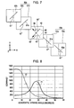
- Fig. 7 is a schematic diagram that illustrates optical conditions in the liquid crystal device.
- Fig. 8 is a graph that represents the viewing angle characteristic of contrast in the liquid crystal device according to the exemplary embodiment of the invention, which is compared with that of a conventional liquid crystal device.
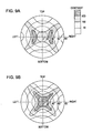
- Fig. 9 is a set of diagrams that illustrate the viewing angle characteristic of contrast in the liquid crystal device according to the exemplary embodiment of the invention, which is compared with that of the conventional liquid crystal device.
- Fig. 10 is a graph that shows a relationship between the retardation of the liquid crystal layer 40 of the liquid crystal device and the contrast offered thereby when viewed obliquely with a horizontal inclination of thirty degrees, which change as the angles of the lower optical axes thereof and those of the upper optical axes thereof are changed.
- Fig. 11 is a graph that shows a relationship between the retardation of the liquid crystal layer 40 of the liquid crystal device and the transmission factor thereof, which change as the angles of the lower optical axes thereof and those of the upper optical axes thereof are changed.
- Fig. 12 is a set of diagrams that illustrate the optical conditions illustrated in Figs. 10 and 11.
- Fig. 13 is an enlarged plain view of a liquid crystal device according to a third exemplary embodiment of the invention.
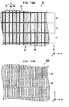
- Fig. 14A is an enlarged plain view of a liquid crystal panel
- Fig. 14B is an enlarged plain view of a barrier mask substrate.
- Fig. 15 is a perspective view of a display device for a car navigation system.
- Fig. 1 is an enlarged plain view of a liquid crystal device 1 according to a first exemplary embodiment of the present invention.
- Fig. 2 is a sectional view that schematically illustrates an exemplary configuration of the liquid crystal device 1 shown in Fig. 1.
- the liquid crystal device 1 is provided with a liquid crystal panel 2, which functions as a display panel, and is further provided with a barrier mask substrate 30 that is adhered to the liquid crystal panel 2 via an adhesive 35.
- the liquid crystal panel 2 has a pair of an element substrate 10 and a counter substrate (i.e., opposite substrate) that is adhered to each other via a frame-patterned sealant, which is not shown in the drawing.
- the distance between the element substrate 10 and the counter substrate 20 is determined by columnar spacers, which are not shown in the drawing.
- the element substrate 10 includes a glass substrate 11 that constitutes a first substrate according to the invention, whereas the counter substrate 20 includes a glass substrate 21 that constitutes a second substrate according to the invention.
- a TN-mode liquid crystal layer 40 is sandwiched between the element substrate 10 and the counter substrate 20.
- the barrier mask substrate 30 includes a glass substrate 31 as its base substance.
- a barrier layer 32 having light-shielding property is deposited on the liquid-crystal-panel-side (2) surface of the glass substrate 31. Opening portions 33 are formed in the barrier layer 32.
- Fig. 3A is an enlarged plain view of the liquid crystal panel 2 that is before being adhered to the barrier mask substrate 30.
- Fig. 3B is an enlarged plain view of the barrier mask substrate 30 that is before being adhered to the liquid crystal panel 2.
- the liquid crystal device 1 illustrated in Fig. 1 is made up of the liquid crystal panel 2 and the barrier mask substrate 30 adhered to each other.
- the shaded region with half-tone dots in Fig. 1 denotes an area that is covered by the barrier layer 32 formed in the barrier mask substrate 30.
- the liquid crystal panel 2 has rectangular pixels 4r, 4g, and 4b (hereafter correctively referred to as "pixel 4" as long as the context allows) that are arrayed in a matrix pattern.
- the pixels 4r perform red-color display.
- the pixels 4g perform green-color display.
- the pixels 4b perform blue-color display.
- the pixels 4r, the pixels 4g, and the pixels 4b are arranged in a repetitive pattern in the order of appearance herein when viewed along the X direction in the drawing. On the other hand, when viewed along the Y direction, the pixels 4 form a stripe pattern.
- each of the groups of the pixels 4r, 4g, and 4b are arranged in such a manner that each color component forms vertical lines in the Y direction so that the entire arrangement is recognized as a vertical stripe pattern according to the drawing.
- a light-shielding layer 14 that is made of a black resin is formed between each adjacent two of the pixels 4.
- each row of the pixels 4 that is aligned in the X direction is referred to as a pixel row 5.
- each one of the pixels 4 contributes to the display of either the first image or the second image.
- the pixels 4 that function to display the first image may be referred to as pixels 4L
- the pixels 4 that function to display the second image may be referred to as pixels 4R.
- the pixels 4L and the pixels 4R are arranged in an alternating order when viewed along the direction of each of the pixel rows 5, that is, the X direction.
- each of the pixels 4L and the pixels 4R is aligned in a line in such a manner that the entire arrangement constitutes a vertical stripe pattern of the pixels 4L and the pixels 4R.
- the barrier layer 32 formed in the barrier mask substrate 30 has, as illustrated in Fig. 3B, the opening portions 33 at regions that substantially overlap the light-shielding layer 14 between the pixels 4L and the pixels 4R when viewed from the normal direction of the liquid crystal panel 2.
- the phrase "between the pixels 4L and the pixels 4R" has a special connotation; it exclusively refers to regions where the pixels 4L lie adjacent to the pixels 4R and they are arrayed in the order of appearance herein (i.e., 4L before 4R) when viewed in a direction from the right to the left in the drawing (i.e., the negative direction along the X axis).
- the phrase "between the pixels 4L and the pixels 4R" does not contain regions where the pixels 4R lie before the adjacent pixels 4L when viewed along the above-identified direction. Therefore, the opening portions 33 are provided for every other line of the light-shielding layer 14 when viewed in the X direction.
- the width of the opening portion 33 is configured to be slightly greater than that of the light-shielding layer 14.
- the element substrate 10 of the liquid crystal device 1 is a so-called TFT array substrate that includes TFT (Thin Film Transistor) elements 22. Each of the TFT elements 22 corresponds to one of the pixels 4.
- the element substrate 10 further includes gate lines (not shown in the drawing), data lines 28, and pixel electrodes 24, though not limited thereto. Each of the gate lines is connected to the corresponding one of the TFT elements 22. The same holds true for the data lines 28 and pixel electrodes 24.
- First, second, third, and fourth component layers are laminated on one surface of the glass substrate 11 of the element substrate 10 that is closer to the liquid crystal layer 40 than the other surface thereof.
- an interlayer insulation film 41, an interlayer insulation film 42, and an interlayer insulation film 43 are interposed between the first component layer and the second component layer, the second component layer and the third component layer, and the third component layer and the fourth component layer, respectively.
- TFD Thin Film Diode
- a gate electrode 22g which constitutes a part of each of the TFT element 22s, is formed on the first component layer that is deposited on the surface of the glass substrate 11.
- the second component layer is deposited over the first component layer with the interlayer insulation film 41 interposed therebetween.
- the interlayer insulation film 41 is made of SiO 2 , SiN, or the like.
- a semiconductor layer 22a made of amorphous silicon is formed on the second component layer at a position that overlaps each of the gate electrodes 22g.
- a source electrode 22s is formed at the source region of the semiconductor layer 22a in such a manner that the source electrode 22s partially overlies the semiconductor layer 22a.
- a drain electrode 22d is formed at the drain region of the semiconductor layer 22a in such a manner that the drain electrode 22d partially overlies the semiconductor layer 22a.
- Each of the TFT elements 22 is made up of the semiconductor layer 22a, the source electrode 22s, the drain electrode 22d, and the gate electrode 22g.
- the third component layer is deposited over the second component layer with the interlayer insulation film 42 interposed therebetween.
- the interlayer insulation film 42 is made of SiO 2 , SiN, or the like.
- the data lines 28 are formed on the third component layer. Each of the data lines 28 is connected to the corresponding source electrode 22s of the TFT element 22 via a contact hole that is formed in (or penetrates through) the interlayer insulation film 42.
- the fourth component layer is deposited over the third component layer with the interlayer insulation film 43 interposed therebetween.
- the interlayer insulation film 43 is made of SiN or the like.
- the pixel electrodes 24 each of which is made of translucent ITO (indium Tin Oxide) are formed on the fourth component layer.
- Each of the pixel electrodes 24 is connected to the corresponding drain electrode 22d of the TFT element 22 via a contact hole that penetrates through the interlayer insulation films 42 and 43.
- An alignment film i.e., orientation film
- polyimide which is not shown in the drawing
- a viewing angle compensation film 51a and a polarizing plate (film) 52a are laminated on the other surface of the glass substrate 11 that is opposite to the above-mentioned one surface thereof which is closer to the liquid crystal layer 40.
- the viewing angle compensation film 51a and the polarizing plate 52a are deposited in the order of appearance herein; in other words, the viewing angle compensation film 51a is deposited on the other surface of the glass substrate 11, and the polarizing plate 52a is deposited on the viewing angle compensation film 51a.
- the viewing angle compensation film 51a corresponds to a first film according to the invention.
- the polarizing plate 52a corresponds to a first polarizing plate according to the invention.
- a combination film made up of the viewing angle compensation film 51a and the polarizing plate 52a deposited on the glass substrate 11 is collectively referred to as an optical film 50a.
- a backlight 48, which irradiates light toward the liquid crystal device 1, is provided at a position that faces to (i.e., is opposed to) the optical film 50a.
- Fig. 4 is a sectional view that schematically illustrates an example of the configuration of the optical film 50a in detail.
- the optical film 50a has a laminated structure that includes an adhesive layer 55, the viewing angle compensation film 51a, and the polarizing plate 52a, which are deposited in the order of appearance herein.
- the polarizing plate 52a is made up of a pair of TAC (cellulose triacetate / triacetyl cellulose) films 53 and a polarizer 54 that contains iodine. In the configuration of the polarizing plate 52a, the iodine-containing polarizer 54 is sandwiched between the pair of TAC films 53.
- the optical film 50a is bonded to the glass substrate 11 by means of the adhesive layer 55.
- Fig. 5 is a schematic sectional view of the liquid crystal layer 40 and the viewing angle compensation film 51a that explains the function of the viewing angle compensation film 51a.
- the viewing angle compensation film 51a contains a flat discotic-type polymer liquid crystal 510 that indicates an optically negative single axiality.
- the viewing angle compensation film 51a is formed as a solidified film of the nematic hybrid orientation/alignment property/structure of the flat discotic-type polymer liquid crystal 510.
- An angle formed by the direction of the normal of a flat disc, which is formed by the discotic-type polymer liquid crystal 510, and the film plane at the upper face of the film is not the same as an angle formed thereby at the lower face thereof, which indicates hybrid orientation (i.e., alignment).
- the above-mentioned angles change progressively (i.e., continually) between the upper face of the film and the lower face thereof.
- the direction obtained by projecting the normal direction of the flat disc plane formed by the discotic-type polymer liquid crystal 510 onto the film surface is referred to as the orientation axis of the viewing angle compensation film 51a.
- the viewing angle compensation film 51 is capable of compensating the tilt of the liquid crystal layer 40 by means of the discotic-type polymer liquid crystal 510. Since the tilt direction of the discotic-type polymer liquid crystal 510 (a molecule having a negative single axiality) contained in the viewing angle compensation film 51a changes progressively, there exists a combination that cancels refractive index anisotropy between the molecule having a negative single axiality and a liquid crystal molecule (a molecule having a positive single axiality) contained in the liquid crystal layer 40. If one focuses attention on such a combination, an index of refraction is equalized regardless of the difference in viewing directions. As a result thereof, it is possible to enhance the viewing angle characteristics of the liquid crystal device 1. In addition thereto, it is further possible to increase contrast that is obtained/perceived when an observer monitors the display of the liquid crystal device 1 at an oblique angle, which improves the visibility of images.
- a plurality of color filters having red, green, and blue colors are formed on one surface of the glass substrate 21 of the counter substrate 20 that is closer to the liquid crystal layer 40 than the other surface thereof.
- the red color filters 12r, green color filters 12g (not shown in the drawing), and blue color filters 12b correspond to the pixels 4r, 4g, and 4b, respectively.
- these color filters may be correctively referred to as color filters 12.
- Each of the color filters 12 functions as a layer that absorbs light having a specified wavelength out of an incident light. Thanks to the color filter 12, transmitted light has any one desired color component (for example, red light, green light, or blue light).
- the light-shielding layer 14 that is made of a black resin is formed between each adjacent two of the pixels 4.
- the common electrode 23 is connected to a constant potential line that is not shown in the drawing. Therefore, the common electrode 23 is maintained at a constant potential level.
- An alignment film, that is, an orientation film, which is made of polyimide, is formed on the surface of the common electrode 23. This orientation film is not shown in the drawing.
- an overcoat film made of a translucent resin may be laminated on the color filters 12 and the light-shielding layer 14. If such an alternative configuration is adopted, the common electrode 23 is formed on the overcoat film.
- the liquid crystal layer 40 is sandwiched between the element substrate 10 and the counter substrate 20.
- the liquid crystal layer is configured to operate in a TN mode.
- the twist angle of the liquid crystal layer 40 is set at 90 degrees (90°).
- a driving voltage is applied between the common electrode 23 and the pixel electrodes 24, an electric field is generated in the liquid crystal layer 40.
- the orientation state of the liquid crystal molecules contained in the liquid crystal layer 40 changes as the electric field occurs.
- the liquid crystal device 1 performs display by utilizing a polarization conversion function that is offered in accordance with the orientation state of the liquid crystal molecules as well as a polarization selection function that is offered by the polarizing plate 52a and a polarizing plate 52b.
- the barrier mask substrate 30 is adhered by means of the adhesive 35 to the other surface of the glass substrate 21 that is opposite to the above-mentioned one surface thereof that is closer to the liquid crystal layer 40.
- the barrier mask substrate 30 includes the glass substrate 31 as its base substance.
- the barrier layer 32 is deposited on the liquid-crystal-layer-side (40) surface of the glass substrate 31.
- the glass substrate 21 is treated by means of chemical etching processing, CMP (Chemical Mechanical Polishing) or the like so as to have a thickness of approximately 50 ⁇ m.
- CMP Chemical Mechanical Polishing
- the liquid crystal device 1 is able to display the first image and the second image each at a preferred angle.
- a viewing angle compensation film 51b and the polarizing plate 52b are laminated on the outer surface of the glass substrate 31, that is, one surface of the glass substrate 31 that is opposite to the other surface that is closer to the glass substrate 21. Note that-the viewing angle compensation film 51b and the polarizing plate 52b are deposited thereon in the order of appearance herein.
- the viewing angle compensation film 51b corresponds to a second film according to the invention, whereas the polarizing plate 52b corresponds to a second polarizing plate according to the invention.
- a combination film made up of the viewing angle compensation film 51b and the polarizing plate 52b deposited on the glass substrate 31 is collectively referred to as an optical film 50b.
- the configuration of the optical film 50b is the same as that of the optical film 50a. The detailed configuration thereof is illustrated in Fig. 4.
- Fig. 6 is a diagram that illustrates a sectional view of the liquid crystal device 1 having the above-described configuration while explaining the relationship between viewing angles and the corresponding observed images. It should be noted that Fig. 6 highlights a plurality of beams of light that pass through the opening portion 33 formed at an area between the pixel 4b (pixel 4R) and the pixel 4r (pixel 4L). The behavior of light that passes through any other opening portion 33 is the same as that illustrated in this drawing. It should be further noted that the thickness of the glass substrate 21 in this drawing is increased in such a manner that it is not in proportion to other components for the purpose of making the explanation of each optical path easier. In order to simplify illustration, the components of the element substrate 10 are omitted from the drawing.
- Display light coming from the pixel 4r passes through the opening portion 33 and then is refracted to change its direction at the time of entering an air layer. Consequently, the display light is observed within a range of visualization angle that is denoted as 9r in the drawing.
- display light coming from the pixel 4g is observed within a range of visualization angle that is denoted as 9g in the drawing
- display light coming from the pixel 4b is observed within a range of visualization angle that is denoted as 9b therein.
- the visualization angle range 9r and the visualization angle range 9b partially overlap with each other.
- the visualization angle range 9r partially overlaps with the visualization angle range 9g. The same applies for the visualization angle range 9b and the visualization angle range 9g.
- the barrier layer 32 blocks the display light coming from the pixel 4b within an angular range VL, which extends from the center to the left, the display light coming from the pixel 4r only is observed in the angular range VL.
- the barrier layer 32 blocks the display light coming from the pixel 4r within an angular range VR, which extends from the center to the right, the display light coming from the pixel 4b only is observed in the angular range VR.
- the first image based on the pixel 4L only is observed in the angular range VL
- the second image based on the pixel 4R only is observed in the angular range VR.
- the liquid crystal device 1 is capable of displaying two different images, one within the angular range VL and the other within the angular range VR. It is possible to adjust both of the angular ranges VL and VR by modifying the width of the opening portion 33, the thickness of the glass substrate 21, and/or any other similar factor.
- each of the angular ranges VL and VR may be set between fifteen degrees and fifty degrees (15-50°) inclusive, when measured from the direction of the normal of the glass substrate 21.
- the center angular range VC which lies between the left angular range VL and the right angular range VR. That is, the center angular range VC constitutes a mixed image area where both of the first image and the second image are observed. This is because the width in the X direction of the opening portion 33 is greater than that of the light-shielding layer 14.
- the liquid crystal device 1 is a so-called “dual-screen” display device that is able to display two different images in directions different from each other concurrently, which are observed obliquely from the left side and the right side at the same time. For this reason, it is preferable that the liquid crystal device 1 offers a wide viewing angle. In particular, it is preferable that the liquid crystal device 1 has a high contrast when monitored from a direction that is slanted by approximately thirty degrees (30°) with respect to the frontal direction thereof. Optical Condition
- Fig. 7 is a schematic diagram that illustrates an example of the optical condition of the liquid crystal device 1.
- the X-axis direction in this drawing corresponds to the horizontal direction at the time of observation, whereas the Y-axis direction in this drawing corresponds to the vertical direction at the time of observation.
- the Y direction is taken as a referential axis for indicating angles.
- a counterclockwise angular direction is denoted with a symbol "+" (plus), whereas a clockwise angular direction is denoted with a symbol "-" (minus).
- the orientation direction 64 of the liquid crystal layer 40 on the surface of the glass substrate 11 forms an angle of positive 45 degrees (+45°) with the Y-axis direction
- the orientation direction 65 of the liquid crystal layer 40 on the surface of the glass substrate 21 forms an angle o negative 45 degrees (-45°) with the Y-axis direction. Therefore, a twist angle 66 of the liquid crystal layer 40 is 90 degrees (90°). More specifically, it is twisted at 90 degrees (90°) in a counterclockwise direction from the glass substrate 21 (upper substrate) to the glass substrate 11 (lower substrate). Therefore, the direction of twelve o'clock (viewed from +Y) constitutes a clear viewing direction.
- the above orientation directions 64 and 65 agree with the direction of rubbing processing of the alignment/orientation film.
- the retardation ( ⁇ nd) of the liquid crystal layer 40 is set at 0.35 ⁇ m.
- the value/symbol ⁇ n denotes the refractive index anisotropy of liquid crystal molecules contained in the liquid crystal layer 40.
- the value/symbol “d” denotes the thickness of the liquid crystal layer 40.
- the above retardation value is smaller than the optimum one that is obtained/assumed when the liquid crystal device 1 is observed from the front thereof. According to such a setting, it is possible to obtain an optimum retardation when the liquid crystal device 1 is observed at an oblique angle because the optical path of light that passes through the liquid crystal layer 40 is relatively long in such a case, which increases the apparent retardation to the light.
- the orientation axis 61a of the viewing angle compensation film 51a has the same angle as that of the absorption axis 62a of the polarizing plate 52a. That is, each of them forms an angle of positive 47 degrees (+47°) with the Y-axis direction.
- each of the orientation axis 61a and the absorption axis 62a is shifted by an angle of two degrees (2°) in a direction that is opposite to the clear viewing direction across the orientation direction 64 of the liquid crystal layer 40 on the surface of the glass substrate 11.
- the orientation axis 61a and the absorption axis 62a may be correctively referred to as lower optical axes.
- the orientation axis 61b of the viewing angle compensation film 51b has the same angle as that of the absorption axis 62b of the polarizing plate 52b. That is, each of them forms an angle of negative 47 degrees (-47°) with the Y-axis direction.
- each of the orientation axis 61b and the absorption axis 62b is shifted by an angle of two degrees (2°) in a direction that is opposite to the clear viewing direction across the orientation direction 65 of the liquid crystal layer 40 on the surface of the glass substrate 21.
- the orientation axis 61b and the absorption axis 62b may be correctively referred to as upper optical axes.
- an angle formed by the lower optical axes and the upper optical axes is ninety-four degrees (94°) with the Y-axis being the center thereof. Thus, it is wider by two degrees (2°) each at the left and the right in comparison with the twist angle 66 of the liquid crystal layer 40. If such a configuration is adopted, the absorption axis 62a of the polarizing plate 52a and the absorption axis 62b of the polarizing plate 52b are not orthogonal to each other when viewed from the front direction (that is, the direction of the normal of the glass substrate 21) but orthogonal to each other when viewed obliquely at a specified inclination.
- the liquid crystal device 1 is capable of offering high-contrast display when monitored at a horizontally inclined direction.
- Fig. 8 is a graph that represents the visual characteristics of display contrast for horizontal (left and right) viewing angle.
- Fig. 9 is a set of contour contrast curves obtained when the viewing angle is modified horizontally and vertically.
- the curve 71 illustrated in Fig. 8 represents the viewing angle characteristic of the liquid crystal device 1 according to the present embodiment of the invention.
- the curve 72 illustrated therein represents the viewing angle characteristic of conventional liquid crystal devices.
- the retardation of the liquid crystal layer is 0.40 ⁇ m.
- both of the absorption axis of the polarizing plate and the orientation axis of the viewing angle compensation film agree with, that is, not shifted from, the orientation direction of the liquid crystal layer on the surface of the substrate.
- the liquid crystal device 1 features an enhanced contrast in the proximity of thirty degrees (30°) in the viewing angle range where the first image and the second image can be observed obliquely from the left and the right.
- the liquid crystal device 1 offers a high contrast of approximately 900, which is well over the contrast of conventional liquid crystal devices, that is, approximately 100.
- the liquid crystal device 1 is capable of performing a high-contrast display at the viewing angle that is most suitable for observation/monitoring of the first image and the second image.
- the invention ensures high visibility of images.
- the retardation of the liquid crystal layer 40 can be made smaller by decreasing the thickness of the liquid crystal layer 40 and by modifying the angles of the viewing angle compensation films 51a and 51b as well as those of the polarizing plates 52a and 52b.
- the thickness of the liquid crystal layer 40 can be reduced if, for example, the height of columnar spacers is lowered. Such a modification makes it easier to determine the height of the spacers. Therefore, the liquid crystal device 1 can be manufactured in an easier manner in comparison with conventional liquid crystal devices.
- FIG. 10 shows a relationship between the retardation of the liquid crystal layer 40 of the liquid crystal device 1 according to the first embodiment of the invention and the contrast offered thereby when viewed obliquely with a horizontal inclination of thirty degrees (30°), which change as the angles of the lower optical axes (i.e., orientation axis 61a and absorption axis 62a) thereof and those of the upper optical axes (i.e., orientation axis 61b and absorption axis 62b) thereof are changed.
- Six curves shown in Fig. 10 indicate examples of a variety of visual characteristics corresponding to a plurality of patterns of angles formed by the lower optical axes and the upper optical axes.
- curves 88CR, 90CR, 92CR, 94CR, 96CR, and 98CR represent visual characteristics obtained when the angles formed by the lower optical axes and the upper optical axes are 88°, 90°, 92°, 94°, 96°, and 98°, respectively.
- Fig. 12 is a set of diagrams that illustrates these optical conditions.
- Fig. 12A shows the orientation directions 64 and 65 of the liquid crystal layer 40 that are twisted by ninety degrees (90°) from each other.
- Fig. 12B illustrates the lower optical axes and the upper optical axes when the angle formed thereby is eighty-eight degrees (88°).
- Fig. 12A shows the orientation directions 64 and 65 of the liquid crystal layer 40 that are twisted by ninety degrees (90°) from each other.
- Fig. 12B illustrates the lower optical axes and the upper optical axes when the angle formed thereby is eighty-eight degrees (88°).
- 12C, 12D, 12E, 12F, and 12G illustrate the lower optical axes and the upper optical axes when the angles formed thereby are 90°, 92°, 94°, 96°, and 98°, respectively.
- the lower optical axes and the upper optical axes are symmetric with respect to the Y direction.
- the viewing angle characteristics change significantly when the optical conditions are changed in the configuration of the liquid crystal device 1 according to the first embodiment of the invention.
- optical condition is not limited to the specific example described above. That is, it may be arbitrarily modified within the technical scope of the invention.
- the absorption axis 62a of the polarizing plate 52a may be shifted from the orientation direction 64 of the liquid crystal layer 40 on the surface of the glass substrate 11 by an angular amount of not less than one degree and not more than three degrees (i.e., a shift range of 1-3° inclusive) in the direction opposite to the twist direction of the liquid crystal layer 40.
- Fig. 11 shows, in the configuration of the liquid crystal device 1 according to the first embodiment of the invention, a relationship between the retardation of the liquid crystal layer 40 and the transmission factor thereof, which change as the angles of the lower optical axes (i.e., orientation axis 61a and absorption axis 62a) thereof and those of the upper optical axes (i.e., orientation axis 61b and absorption axis 62b) thereof are changed.
- Six curves shown in Fig. 11 indicate examples of a variety of visual characteristics corresponding to a plurality of patterns of angles formed by the lower optical axes and the upper optical axes, which is similar to Fig. 10.
- curves 88T, 90T, 92T, 94T, 96T, and 98T represent visual characteristics obtained when the angles formed by the lower optical axes and the upper optical axes are 88°, 90°, 92°, 94°, 96°, and 98°, respectively.
- the arrangements of the lower optical axes and the upper optical axes in these 88°, 90°, 92°, 94°, 96°, and 98° angular conditions are illustrated in Figs. 12B, 12C, 12D, 12E, 12F, and 12G, respectively.
- the transmission factor increases as the retardation of the liquid crystal layer 40 increases.
- the transmission factor is raised, the visibility of the first image and the second image is enhanced.
- the incremental change of the transmission factor is relatively small when the retardation of the liquid crystal layer 40 is set at 0.30 ⁇ m or greater.
- the transmission factor decreases at a relatively large drop rate when the retardation of the liquid crystal layer 40 is less than 0.30 ⁇ m. For this reason, it is preferable to set the retardation of the liquid crystal layer 40 at 0.30 ⁇ m or greater for the purpose of ensuring a high transmission factor.
- a liquid crystal device 1B according to a third exemplary embodiment of the invention is explained below.
- the arrangement positions of the pixels 4L, the pixels 4R, and the opening portions 33 of the liquid crystal device 1B are modified in comparison with those of the liquid crystal device 1 according to the first embodiment of the invention.
- the configuration of the liquid crystal device 1B according to the present embodiment of the invention is the same as that of the liquid crystal device 1 according to the first embodiment of the invention. Therefore, in the following description, the liquid crystal device 1B according to the present embodiment of the invention is explained while highlighting the above difference.
- the same reference numerals are consistently used in Fig. 13 and Fig. 14 for the same components as those of the liquid crystal device 1 illustrated in Fig. 1 and Fig. 3 to omit any redundant explanation thereof.
- Fig. 13 is an enlarged plain view of a liquid crystal device 1B according to the third exemplary embodiment of the invention.
- the liquid crystal device 1B is also a so-called dual-screen display device that is able to display two different images, the first and second images, in directions different from each other concurrently.
- the liquid crystal device 1B is provided with a liquid crystal panel 2B that functions as a display panel and is further provided with a barrier mask substrate 30B that is adhered to the liquid crystal panel 2B via an adhesive 35, which is the same configuration as that of the liquid crystal device 1.
- Fig. 14A is an enlarged plain view of the liquid crystal panel 2B that is before being adhered to the barrier mask substrate 30B.
- FIG. 14B is an enlarged plain view of the barrier mask substrate 30B that is before being adhered to the liquid crystal panel 2B.
- the shaded region with half-tone dots in Fig. 13 denotes an area that is covered by the barrier layer 32 formed in the barrier mask substrate 30B.
- the liquid crystal panel 2B has rectangular pixels 4r, 4g, and 4b.
- the pixels 4r perform red-color display.
- the pixels 4g perform green-color display.
- the pixels 4b perform blue-color display.
- the pixels 4r, the pixels 4g, and the pixels 4b are arranged in a repetitive pattern in the order of appearance herein when viewed along the X direction in the drawing.
- the pixels 4 form a stripe pattern. That is, each of the groups of the pixels 4r, 4g, and 4b are arranged in such a manner that each color component forms vertical lines in the Y direction so that the entire arrangement is recognized as a vertical stripe pattern according to the drawing.
- a light-shielding layer 14 is formed between each adjacent two of the pixels 4.
- Each of the pixels 4 functions as either one of a pixel 4L that displays the first image and a pixel 4R that displays the second image.
- the pixels 4L and 4R are arranged in an alternating order when viewed along the X direction.
- the pixels 4L and 4R are arranged in an alternating order when viewed along the Y direction that is orthogonal to the X direction. That is, when viewed along the X direction of each pixel row 5, the pixel 4L, the light-shielding layer 14, the pixel 4R, and the light-shielding layer 14 are arranged in the order of appearance herein, which constitute a unit of cyclic array.
- the above-mentioned unit of cyclic arrangement is shifted by a half pitch cyclic amount between each of vertically adjacent two pixel rows 5.
- the pixels 4L and the pixels 4R are arrayed in an alternating order.
- the positions of the opening portions 33 formed in the barrier layer 32 of the barrier mask substrate 30B are modified from those of the liquid crystal device 1 according to the first embodiment of the invention.
- the barrier layer 32 formed in the barrier mask substrate 30B has the opening portions 33 at regions that substantially overlap the light-shielding layer 14 between the pixels 4L and the pixels 4R when viewed from the normal direction of the liquid crystal panel 2B.
- the phrase "between the pixels 4L and the pixels 4R” has a special connotation; it exclusively refers to regions where the pixels 4L lie adjacent to the pixels 4R and they are arrayed in the order of appearance herein (i.e., 4L before 4R) when viewed in a direction from the right to the left in the drawing (i.e., the negative direction along the X axis). Accordingly, the phrase “between the pixels 4L and the pixels 4R” does not contain regions where the pixels 4R lie before the adjacent pixels 4L when viewed along the above-identified direction. Therefore, the opening portions 33 are provided for every other line of the light-shielding layer 14 when viewed both in the X direction and in the Y direction.
- the opening portions 33 are staggered (i.e., shifted) by a half pitch cyclic amount between each of vertically adjacent two pixel rows 5 so that the layout of the opening portions 33 corresponds to the array pattern of the pixels 4L and 4R.
- the slit-shaped opening portions 33 each of which has a length that is substantially equal to the Y-axial width of the pixel row 5 are arranged in an oblique direction.
- the barrier layer 32 having such an array pattern is called as a step barrier.
- the width of the opening portion 33 is configured to be slightly greater than that of the light-shielding layer 14.
- a distance between two of the pixels 4L that are closest to each other among the pixels 4L that contribute to the same color-phase display equals a value obtained by multiplying that of a normal liquid crystal device which does not perform dual-screen display by ⁇ 2. Therefore, the resolution of display according to the liquid crystal device 1B having the above-mentioned step barrier configuration equals a value that is calculated by multiplying that of the normal liquid crystal device by 1/ ⁇ 2. The same feature applies for the pixels 4R.
- display resolution of the liquid crystal device 1 according to the first embodiment of the invention which has a stripe array pattern of the pixels 4L and 4R, is a half (1/2) of that of a normal liquid crystal device. Therefore, the above-described configuration according to the present embodiment of the invention makes it possible to improve the resolution of display in comparison with that of the first embodiment of the invention, specifically, by a multiplication factor of ⁇ 2.
- the liquid crystal device 1B is also capable of displaying two different images, for example, the first image within the angular range VL and the second image within the angular range VR, as the liquid crystal device 1 according to the first embodiment of the invention does.
- the retardation of the liquid crystal layer 40 of the liquid crystal device 1B is set at 0.35 ⁇ m, which is the same as that of the liquid crystal device 1 according to the first embodiment of the invention.
- each of the orientation axis 61a of the viewing angle compensation film 51a and the absorption axis 62a of the polarizing plate 52a is shifted from the orientation direction 64 of the liquid crystal layer 40 on the surface of the glass substrate 11 (+45°) by the angular amount of two degrees (2°) in the direction opposite to the twist direction of the liquid crystal layer 40
- each of the orientation axis 61b of the viewing angle compensation film 51b and the absorption axis 62b of the polarizing plate 52b is shifted from the orientation direction 65 of the liquid crystal layer 40 on the surface of the glass substrate 21 (-45°) by the angular amount of two degrees (2°) in the direction opposite to the twist direction of the liquid crystal layer 40.
- the liquid crystal device 1B of the present embodiment of the invention is also capable of performing a high-contrast display at the viewing angle that is most suitable for observation/monitoring of the first image and the second image, as the liquid crystal device 1 of the first embodiment of the invention does.
- the invention ensures high visibility of images.
- the liquid crystal device 1 described above can be used, as an example of various applications thereof, in a display device 100 illustrated in Fig. 15, which makes up a car navigation system among various kinds of electronic apparatuses. Thanks to the liquid crystal device 1 built in the display section 110 thereof, the display device 100 is capable of displaying two different images in directions different from each other at the same time. For example, the display device 100 is capable of displaying a map image toward a driver's seat while displaying movie pictures toward a front passenger's seat at the same time. In such an application, the invention makes it possible to offer high-quality display with a high contrast.
- the liquid crystal device 1 can be implemented as a variety of electronic apparatuses, including but not limited to, a mobile computer, a digital camera, a digital video camera, automobile-installed equipment, audio equipment, in addition to the display device 100 described above.
- the liquid crystal device 1 displays two images in directions different from each other at the same time. Notwithstanding the foregoing, the invention may be modified in such a manner that the liquid crystal device displays three or more images concurrently.
- the liquid crystal device can be modified to display three or more images concurrently by providing pixels 4C that display a third image in addition to the pixels 4L that display the first image and the pixels 4R that display the second image, and by emitting the transmitted light toward directions different from one another by means of the barrier layer 32 of the barrier mask substrate 30. In such a configuration, it is possible to control the display directions thereof by adjusting the distance between the color filters 12 and the barrier layer 32.
Landscapes
- Physics & Mathematics (AREA)
- Nonlinear Science (AREA)
- Mathematical Physics (AREA)
- Chemical & Material Sciences (AREA)
- Crystallography & Structural Chemistry (AREA)
- General Physics & Mathematics (AREA)
- Optics & Photonics (AREA)
- Liquid Crystal (AREA)
- Spectroscopy & Molecular Physics (AREA)
- Polarising Elements (AREA)
Abstract
Description
- The present invention relates to a liquid crystal device that displays at least two images in directions different from each other or one another at the same time. The present invention further relates to an electronic apparatus that is provided with such a liquid crystal device.
- As a known general configuration, a liquid crystal device has a pair of substrates and a liquid crystal layer that is sandwiched between the pair of substrates. A known liquid crystal device of the related art has a barrier mask substrate that is provided on the surface of one of the pair of the substrates described above. The barrier mask substrate has a barrier layer through which openings are formed. With such a configuration, the above-mentioned known liquid crystal device of the related art is capable of displaying two images in directions different from each other at the same time.
Japanese Patent No. 2,857,429 - It is further known in the art that, as an exemplary application thereof, two observers can monitor two images on an individual basis, which means that one person can view one of two images obliquely from the left side while the other person can view the other image obliquely from the right side, which is achieved by making the display directions of the above-mentioned two images substantially different from each other. In a liquid crystal device that can perform "dual-screen" (i.e., in a virtual sense) display as described above, each of the observers monitors display not from the normal direction of the substrate (i.e., from the front direction) but mainly from an oblique angle thereof.
- Since a typical liquid crystal device is configured to offer the maximum display contrast when viewed in the front direction thereof, disadvantageously, it is difficult to ensure a satisfactory contrast when viewed at an oblique angle. For this reason, if_such a liquid crystal device is used for a dual-screen display application without adopting any effective technical solution, the display contrast of individual left and right images at their optimum angle of view for display will be poor, which deteriorates the visibility of the individual images.
- An advantage of some aspects of the invention is to provide a liquid crystal device and an electronic apparatus that makes it possible to enhance the display contrast of individual (for example, left and right, or first and second, though not limited thereto) images at their optimum angle of view for display so as to improve the visibility of the individual images.
- In order to address the above-identified problem without any limitation thereto, the invention provides, as a first aspect thereof, a liquid crystal device that displays at least two images in directions different from each other or one another at the same time, the liquid crystal device including: a first substrate that has a translucent property; a second substrate that is opposed to the first substrate, the second substrate having a translucent property; a liquid crystal layer that is interposed between the first substrate and the second substrate, the liquid crystal layer having a twist angle of ninety degrees or in the neighborhood thereof; a first polarizing plate that is provided at a layer opposite to the liquid crystal layer with the first substrate being interposed therebetween; and a second polarizing plate that is provided at a layer opposite to the liquid crystal layer with the second substrate being interposed therebetween, wherein the absorption axis of the first polarizing plate is shifted from an orientation direction of the liquid crystal layer on the surface of the first substrate by an angular amount of not less than one degree and not more than three degrees in the direction opposite to the twist direction of the liquid crystal layer, and the absorption axis of the second polarizing plate is shifted from an orientation direction of the liquid crystal layer on the surface of the second substrate by an angular amount of not less than one degree and not more than three degrees in the direction opposite to the twist direction of the liquid crystal layer.
- According to such a configuration, the absorption axis of the first polarizing plate and the absorption axis of the second polarizing plate are not orthogonal to each other when viewed from the front direction (that is, the direction of the normal of the substrate) but orthogonal to each other when viewed obliquely at a specified inclination. As a result thereof, the maximum contrast is obtained when viewed obliquely at the specified inclination. Specifically, the maximum contrast is obtained when viewed from a direction orthogonal to the clear viewing direction, which is determined by the twist direction of the liquid crystal layer. Therefore, the invention makes it possible to enhance the display contrast of individual left and right images at their optimum angle of view for display so as to improve the visibility of the individual images. Herein, the phrase "the direction opposite to the twist direction (i.e., twist angle) of the liquid crystal layer" means the following direction. That is, when viewed from the second-substrate side, in a case where the liquid crystal layer is twisted counterclockwise from the second substrate toward the first substrate, "the direction opposite to the twist direction of the liquid crystal layer" means the counterclockwise direction for the absorption axis of the first polarizing plate whereas "the direction opposite to the twist direction of the liquid crystal layer" means the clockwise direction for the absorption axis of the second polarizing plate. On the other hand, when viewed from the second-substrate side, in a case where the liquid crystal layer is twisted clockwise from the second substrate toward the first substrate, "the direction opposite to the twist direction of the liquid crystal layer" means the clockwise direction for the absorption axis of the first polarizing plate whereas "the direction opposite to the twist direction of the liquid crystal layer" means the counterclockwise direction for the absorption axis of the second polarizing plate. In other words, "the direction opposite to the twist direction of the liquid crystal layer" means, for the absorption axis of the first polarizing plate, the direction that is opposite to the clear viewing direction across the orientation direction of the liquid crystal layer on the surface of the first substrate, that is, the direction that is opposite to the clear viewing direction with the orientation direction of the liquid crystal layer on the surface of the first substrate being sandwiched therebetween. Similarly, "the direction opposite to the twist direction of the liquid crystal layer" means, for the absorption axis of the second polarizing plate, the direction that is opposite to the clear viewing direction across the orientation direction of the liquid crystal layer on the surface of the second substrate, that is, the direction that is opposite to the clear viewing direction with the orientation direction of the liquid crystal layer on the surface of the second substrate being sandwiched therebetween. It should be noted that other constituent element(s) that has a translucent property (i.e., other translucent constituent element(s)) may be interposed between the first substrate and the first polarizing plate and/or between the second substrate and the second polarizing plate.
- In the above configuration of the liquid crystal device according to the first aspect of the invention, it is preferable that the retardation of the liquid crystal layer is not less than 0.30 µm and not more than 0.37 µm. The retardation within the range described above is a value that is smaller than the optimum one that is obtained/assumed when the liquid crystal device is observed from the front thereof. According to such a configuration, it is possible to obtain an optimum retardation when the liquid crystal device is observed at an oblique angle because the optical path of light that passes through the liquid crystal layer is relatively long in such a setting, which increases the apparent retardation to the light. In particular, it is possible to obtain sufficient brightness if the retardation is set at a value that is not less than 0.30 µm; and in addition, it is possible to obtain optimum contrast when viewed at an inclined direction if the retardation is set at a value that is not more than 0.37 µm. Therefore, the above configuration makes it possible to enhance the display contrast of individual images at their optimum angle of view for display so as to improve the visibility of the individual images.
- It is preferable that the liquid crystal device according to the first aspect of the invention further comprises, in addition to the configuration described above: a first film that is interposed between the first substrate and the first polarizing plate, the first film having an orientation axis that is substantially in alignment with the absorption axis of the first polarizing plate, the first film containing discotic polymer liquid crystal that has hybrid orientation; and a second film that is interposed between the second substrate and the second polarizing plate, the second film having an orientation axis that is substantially in alignment with the absorption axis of the second polarizing plate, the second film containing discotic polymer liquid crystal that has hybrid orientation.
According to such a configuration, it is possible to widen the viewing angle range within which high contrast is obtained thanks to the viewing angle compensation functions of the first and second films. Therefore, the invention makes it possible to enhance the display contrast of individual images at their optimum angle of view for display so as to improve the visibility of the individual images. - In the above configuration of the liquid crystal device according to the first aspect of the invention, it is preferable that the retardation of the liquid crystal layer is 0.32 µm or in the neighborhood thereof; each of the absorption axis of the first polarizing plate and the orientation axis of the first film is shifted from the orientation direction of the liquid crystal layer on the surface of the first substrate by the angular amount of two degrees or in the neighborhood thereof in the direction opposite to the twist direction of the liquid crystal layer; and each of the absorption axis of the second polarizing plate and the orientation axis of the second film is shifted from the orientation direction of the liquid crystal layer on the surface of the second substrate by the angular amount of two degrees or in the neighborhood thereof in the direction opposite to the twist direction of the liquid crystal layer. According to such a configuration, it is possible to enhance the display contrast of individual images at their optimum angle of view for display.
- In the above configuration of the liquid crystal device according to the first aspect of the invention, it is preferable that the retardation of the liquid crystal layer is 0.35 µm or in the neighborhood thereof; each of the absorption axis of the first polarizing plate and the orientation axis of the first film is shifted from the orientation direction of the liquid crystal layer on the surface of the first substrate by the angular amount of two degrees or in the neighborhood thereof in the direction opposite to the twist direction of the liquid crystal layer; and each of the absorption axis of the second polarizing plate and the orientation axis of the second film is shifted from the orientation direction of the liquid crystal layer on the surface of the second substrate by the angular amount of two degrees or in the neighborhood thereof in the direction opposite to the twist direction of the liquid crystal layer. According to such a configuration, it is possible to enhance the display contrast of individual images at their optimum angle of view for display while increasing display brightness.
- In order to address the above-identified problem without any limitation thereto, the invention provides, as a second aspect thereof, an electronic apparatus that has the liquid crystal device having the configuration described above in a display section thereof. According to such a configuration, it is possible to provide an electronic apparatus that is capable of displaying at least two images in directions different from each other or one another at the same time, and offering high-quality display with high contrast at the viewing angle that is most suitable for observation/monitoring of these individual images.
- The invention will be described with reference to the accompanying drawings, wherein like numbers reference like elements.
- Fig. 1 is an enlarged plain view of a liquid crystal device according to a first exemplary embodiment of the invention.
- Fig. 2 is a sectional view that schematically illustrates an exemplary configuration of the liquid crystal device shown in Fig. 1.
- Fig. 3A is an enlarged plain view of a liquid crystal panel, whereas Fig. 3B is an enlarged plain view of a barrier mask substrate.
- Fig. 4 is a sectional view that schematically illustrates an example of the configuration of an optical film in detail.
- Fig. 5 is a schematic sectional view of a liquid crystal layer and a viewing angle compensation film that explains the function of the viewing angle compensation film.
- Fig. 6 is a diagram that illustrates a sectional view of the liquid crystal device illustrated in Fig. 1 while explaining the relationship between viewing angles and the corresponding observed images.
- Fig. 7 is a schematic diagram that illustrates optical conditions in the liquid crystal device.
- Fig. 8 is a graph that represents the viewing angle characteristic of contrast in the liquid crystal device according to the exemplary embodiment of the invention, which is compared with that of a conventional liquid crystal device.
- Fig. 9 is a set of diagrams that illustrate the viewing angle characteristic of contrast in the liquid crystal device according to the exemplary embodiment of the invention, which is compared with that of the conventional liquid crystal device.
- Fig. 10 is a graph that shows a relationship between the retardation of the
liquid crystal layer 40 of the liquid crystal device and the contrast offered thereby when viewed obliquely with a horizontal inclination of thirty degrees, which change as the angles of the lower optical axes thereof and those of the upper optical axes thereof are changed. - Fig. 11 is a graph that shows a relationship between the retardation of the
liquid crystal layer 40 of the liquid crystal device and the transmission factor thereof, which change as the angles of the lower optical axes thereof and those of the upper optical axes thereof are changed. - Fig. 12 is a set of diagrams that illustrate the optical conditions illustrated in Figs. 10 and 11.
- Fig. 13 is an enlarged plain view of a liquid crystal device according to a third exemplary embodiment of the invention.
- Fig. 14A is an enlarged plain view of a liquid crystal panel, whereas Fig. 14B is an enlarged plain view of a barrier mask substrate.
- Fig. 15 is a perspective view of a display device for a car navigation system.
- With reference to accompanying drawings, exemplary embodiments of the invention are described below. It should be noted that, in the accompanying drawings that are mentioned below, the dimensions and/or scales of constituent elements are modified from those that will be adopted in an actual implementation of the invention for the purpose of making them easily recognizable in each illustration.
- Fig. 1 is an enlarged plain view of a
liquid crystal device 1 according to a first exemplary embodiment of the present invention. Fig. 2 is a sectional view that schematically illustrates an exemplary configuration of theliquid crystal device 1 shown in Fig. 1. As illustrated in Fig. 2, theliquid crystal device 1 is provided with aliquid crystal panel 2, which functions as a display panel, and is further provided with abarrier mask substrate 30 that is adhered to theliquid crystal panel 2 via an adhesive 35. - The
liquid crystal panel 2 has a pair of anelement substrate 10 and a counter substrate (i.e., opposite substrate) that is adhered to each other via a frame-patterned sealant, which is not shown in the drawing. The distance between theelement substrate 10 and thecounter substrate 20 is determined by columnar spacers, which are not shown in the drawing. Theelement substrate 10 includes aglass substrate 11 that constitutes a first substrate according to the invention, whereas thecounter substrate 20 includes aglass substrate 21 that constitutes a second substrate according to the invention. A TN-modeliquid crystal layer 40 is sandwiched between theelement substrate 10 and thecounter substrate 20. Thebarrier mask substrate 30 includes aglass substrate 31 as its base substance. Abarrier layer 32 having light-shielding property is deposited on the liquid-crystal-panel-side (2) surface of theglass substrate 31. Openingportions 33 are formed in thebarrier layer 32. - Fig. 3A is an enlarged plain view of the
liquid crystal panel 2 that is before being adhered to thebarrier mask substrate 30. Fig. 3B is an enlarged plain view of thebarrier mask substrate 30 that is before being adhered to theliquid crystal panel 2. Theliquid crystal device 1 illustrated in Fig. 1 is made up of theliquid crystal panel 2 and thebarrier mask substrate 30 adhered to each other. The shaded region with half-tone dots in Fig. 1 denotes an area that is covered by thebarrier layer 32 formed in thebarrier mask substrate 30. - As illustrated in Fig. 3A, the
liquid crystal panel 2 hasrectangular pixels pixel 4" as long as the context allows) that are arrayed in a matrix pattern. Thepixels 4r perform red-color display. Thepixels 4g perform green-color display. Thepixels 4b perform blue-color display. It should be noted that thepixels 4r, thepixels 4g, and thepixels 4b are arranged in a repetitive pattern in the order of appearance herein when viewed along the X direction in the drawing. On the other hand, when viewed along the Y direction, thepixels 4 form a stripe pattern. That is, each of the groups of thepixels shielding layer 14 that is made of a black resin is formed between each adjacent two of thepixels 4. In the following description, each row of thepixels 4 that is aligned in the X direction is referred to as apixel row 5. - Each one of the
pixels 4 contributes to the display of either the first image or the second image. In this specification, thepixels 4 that function to display the first image may be referred to aspixels 4L, whereas thepixels 4 that function to display the second image may be referred to aspixels 4R. In the present embodiment of the invention, thepixels 4L and thepixels 4R are arranged in an alternating order when viewed along the direction of each of thepixel rows 5, that is, the X direction. On the other hand, when viewed along the Y direction, each of thepixels 4L and thepixels 4R is aligned in a line in such a manner that the entire arrangement constitutes a vertical stripe pattern of thepixels 4L and thepixels 4R. - The
barrier layer 32 formed in thebarrier mask substrate 30 has, as illustrated in Fig. 3B, the openingportions 33 at regions that substantially overlap the light-shielding layer 14 between thepixels 4L and thepixels 4R when viewed from the normal direction of theliquid crystal panel 2. Herein, it should be particularly noted that the phrase "between thepixels 4L and thepixels 4R" has a special connotation; it exclusively refers to regions where thepixels 4L lie adjacent to thepixels 4R and they are arrayed in the order of appearance herein (i.e., 4L before 4R) when viewed in a direction from the right to the left in the drawing (i.e., the negative direction along the X axis). Accordingly, the phrase "between thepixels 4L and thepixels 4R" does not contain regions where thepixels 4R lie before theadjacent pixels 4L when viewed along the above-identified direction. Therefore, the openingportions 33 are provided for every other line of the light-shielding layer 14 when viewed in the X direction. The width of the openingportion 33 is configured to be slightly greater than that of the light-shielding layer 14. - Next, with reference to Fig. 2, the configuration of the
liquid crystal device 1 having theliquid crystal panel 2 illustrated in Fig. 3A and thebarrier mask substrate 30 illustrated in Fig. 3B adhered to each other (that is, the configuration illustrated in Fig. 1) is explained in detail below. - The
element substrate 10 of theliquid crystal device 1 is a so-called TFT array substrate that includes TFT (Thin Film Transistor)elements 22. Each of theTFT elements 22 corresponds to one of thepixels 4. Theelement substrate 10 further includes gate lines (not shown in the drawing),data lines 28, andpixel electrodes 24, though not limited thereto. Each of the gate lines is connected to the corresponding one of theTFT elements 22. The same holds true for the data lines 28 andpixel electrodes 24. First, second, third, and fourth component layers are laminated on one surface of theglass substrate 11 of theelement substrate 10 that is closer to theliquid crystal layer 40 than the other surface thereof. In order to prevent the occurrence of a short-circuit malfunction between adjacent ones of these component layers, aninterlayer insulation film 41, aninterlayer insulation film 42, and aninterlayer insulation film 43 are interposed between the first component layer and the second component layer, the second component layer and the third component layer, and the third component layer and the fourth component layer, respectively. It should be noted that TFD (Thin Film Diode) elements each having two terminals or the like may be used as a substitute for theTFT elements 22 each having three terminals. These elements function as switching devices. - A
gate electrode 22g, which constitutes a part of each of theTFT element 22s, is formed on the first component layer that is deposited on the surface of theglass substrate 11. - The second component layer is deposited over the first component layer with the
interlayer insulation film 41 interposed therebetween. Theinterlayer insulation film 41 is made of SiO2, SiN, or the like. Asemiconductor layer 22a made of amorphous silicon is formed on the second component layer at a position that overlaps each of thegate electrodes 22g. Asource electrode 22s is formed at the source region of thesemiconductor layer 22a in such a manner that thesource electrode 22s partially overlies thesemiconductor layer 22a. On the other hand, adrain electrode 22d is formed at the drain region of thesemiconductor layer 22a in such a manner that thedrain electrode 22d partially overlies thesemiconductor layer 22a. Each of theTFT elements 22 is made up of thesemiconductor layer 22a, thesource electrode 22s, thedrain electrode 22d, and thegate electrode 22g. - The third component layer is deposited over the second component layer with the
interlayer insulation film 42 interposed therebetween. Theinterlayer insulation film 42 is made of SiO2, SiN, or the like. The data lines 28 are formed on the third component layer. Each of the data lines 28 is connected to thecorresponding source electrode 22s of theTFT element 22 via a contact hole that is formed in (or penetrates through) theinterlayer insulation film 42. - The fourth component layer is deposited over the third component layer with the
interlayer insulation film 43 interposed therebetween. Theinterlayer insulation film 43 is made of SiN or the like. Thepixel electrodes 24 each of which is made of translucent ITO (indium Tin Oxide) are formed on the fourth component layer. Each of thepixel electrodes 24 is connected to thecorresponding drain electrode 22d of theTFT element 22 via a contact hole that penetrates through theinterlayer insulation films - A viewing
angle compensation film 51a and a polarizing plate (film) 52a are laminated on the other surface of theglass substrate 11 that is opposite to the above-mentioned one surface thereof which is closer to theliquid crystal layer 40. The viewingangle compensation film 51a and thepolarizing plate 52a are deposited in the order of appearance herein; in other words, the viewingangle compensation film 51a is deposited on the other surface of theglass substrate 11, and thepolarizing plate 52a is deposited on the viewingangle compensation film 51a. The viewingangle compensation film 51a corresponds to a first film according to the invention. Thepolarizing plate 52a corresponds to a first polarizing plate according to the invention. In the following description, a combination film made up of the viewingangle compensation film 51a and thepolarizing plate 52a deposited on theglass substrate 11 is collectively referred to as anoptical film 50a. Abacklight 48, which irradiates light toward theliquid crystal device 1, is provided at a position that faces to (i.e., is opposed to) theoptical film 50a. - Fig. 4 is a sectional view that schematically illustrates an example of the configuration of the
optical film 50a in detail. Theoptical film 50a has a laminated structure that includes anadhesive layer 55, the viewingangle compensation film 51a, and thepolarizing plate 52a, which are deposited in the order of appearance herein. Thepolarizing plate 52a is made up of a pair of TAC (cellulose triacetate / triacetyl cellulose)films 53 and apolarizer 54 that contains iodine. In the configuration of thepolarizing plate 52a, the iodine-containingpolarizer 54 is sandwiched between the pair ofTAC films 53. Theoptical film 50a is bonded to theglass substrate 11 by means of theadhesive layer 55. - Fig. 5 is a schematic sectional view of the
liquid crystal layer 40 and the viewingangle compensation film 51a that explains the function of the viewingangle compensation film 51a. The viewingangle compensation film 51a contains a flat discotic-typepolymer liquid crystal 510 that indicates an optically negative single axiality. The viewingangle compensation film 51a is formed as a solidified film of the nematic hybrid orientation/alignment property/structure of the flat discotic-typepolymer liquid crystal 510. An angle formed by the direction of the normal of a flat disc, which is formed by the discotic-typepolymer liquid crystal 510, and the film plane at the upper face of the film is not the same as an angle formed thereby at the lower face thereof, which indicates hybrid orientation (i.e., alignment). The above-mentioned angles change progressively (i.e., continually) between the upper face of the film and the lower face thereof. The direction obtained by projecting the normal direction of the flat disc plane formed by the discotic-typepolymer liquid crystal 510 onto the film surface is referred to as the orientation axis of the viewingangle compensation film 51a. - The viewing angle compensation film 51 is capable of compensating the tilt of the
liquid crystal layer 40 by means of the discotic-typepolymer liquid crystal 510. Since the tilt direction of the discotic-type polymer liquid crystal 510 (a molecule having a negative single axiality) contained in the viewingangle compensation film 51a changes progressively, there exists a combination that cancels refractive index anisotropy between the molecule having a negative single axiality and a liquid crystal molecule (a molecule having a positive single axiality) contained in theliquid crystal layer 40. If one focuses attention on such a combination, an index of refraction is equalized regardless of the difference in viewing directions. As a result thereof, it is possible to enhance the viewing angle characteristics of theliquid crystal device 1. In addition thereto, it is further possible to increase contrast that is obtained/perceived when an observer monitors the display of theliquid crystal device 1 at an oblique angle, which improves the visibility of images. - Now, referring back to Fig. 2, we continue to explain the configuration of the
liquid crystal device 1. A plurality of color filters having red, green, and blue colors are formed on one surface of theglass substrate 21 of thecounter substrate 20 that is closer to theliquid crystal layer 40 than the other surface thereof. Thered color filters 12r,green color filters 12g (not shown in the drawing), andblue color filters 12b correspond to thepixels shielding layer 14 that is made of a black resin is formed between each adjacent two of thepixels 4. Acommon electrode 23, which is made of translucent ITO, is formed on the surface of the color filters 12 and the light-shielding layer 14. Thecommon electrode 23 is connected to a constant potential line that is not shown in the drawing. Therefore, thecommon electrode 23 is maintained at a constant potential level. An alignment film, that is, an orientation film, which is made of polyimide, is formed on the surface of thecommon electrode 23. This orientation film is not shown in the drawing. As an example of alternative configurations, an overcoat film made of a translucent resin may be laminated on the color filters 12 and the light-shielding layer 14. If such an alternative configuration is adopted, thecommon electrode 23 is formed on the overcoat film. - As has already been described, the
liquid crystal layer 40 is sandwiched between theelement substrate 10 and thecounter substrate 20. The liquid crystal layer is configured to operate in a TN mode. The twist angle of theliquid crystal layer 40 is set at 90 degrees (90°). When a driving voltage is applied between thecommon electrode 23 and thepixel electrodes 24, an electric field is generated in theliquid crystal layer 40. The orientation state of the liquid crystal molecules contained in theliquid crystal layer 40 changes as the electric field occurs. Theliquid crystal device 1 performs display by utilizing a polarization conversion function that is offered in accordance with the orientation state of the liquid crystal molecules as well as a polarization selection function that is offered by thepolarizing plate 52a and apolarizing plate 52b. - The
barrier mask substrate 30 is adhered by means of the adhesive 35 to the other surface of theglass substrate 21 that is opposite to the above-mentioned one surface thereof that is closer to theliquid crystal layer 40. Thebarrier mask substrate 30 includes theglass substrate 31 as its base substance. Thebarrier layer 32 is deposited on the liquid-crystal-layer-side (40) surface of theglass substrate 31. - The
glass substrate 21 is treated by means of chemical etching processing, CMP (Chemical Mechanical Polishing) or the like so as to have a thickness of approximately 50µm. Through such chemical processing, it is possible to adjust the distance between the color filters 12, which emit light to be displayed in a practical sense, and the openingportions 33 of thebarrier layer 32. As a result of the adjustment of the distance therebetween, it is possible to adjust an angle of the optical path leading from each of the color filters 12 to thecorresponding opening portion 33. By this means, theliquid crystal device 1 is able to display the first image and the second image each at a preferred angle. - A viewing
angle compensation film 51b and thepolarizing plate 52b are laminated on the outer surface of theglass substrate 31, that is, one surface of theglass substrate 31 that is opposite to the other surface that is closer to theglass substrate 21. Note that-the viewingangle compensation film 51b and thepolarizing plate 52b are deposited thereon in the order of appearance herein. The viewingangle compensation film 51b corresponds to a second film according to the invention, whereas thepolarizing plate 52b corresponds to a second polarizing plate according to the invention. In the following description, a combination film made up of the viewingangle compensation film 51b and thepolarizing plate 52b deposited on theglass substrate 31 is collectively referred to as anoptical film 50b. The configuration of theoptical film 50b is the same as that of theoptical film 50a. The detailed configuration thereof is illustrated in Fig. 4. - Fig. 6 is a diagram that illustrates a sectional view of the
liquid crystal device 1 having the above-described configuration while explaining the relationship between viewing angles and the corresponding observed images. It should be noted that Fig. 6 highlights a plurality of beams of light that pass through the openingportion 33 formed at an area between thepixel 4b (pixel 4R) and thepixel 4r (pixel 4L). The behavior of light that passes through any other openingportion 33 is the same as that illustrated in this drawing. It should be further noted that the thickness of theglass substrate 21 in this drawing is increased in such a manner that it is not in proportion to other components for the purpose of making the explanation of each optical path easier. In order to simplify illustration, the components of theelement substrate 10 are omitted from the drawing. - Display light coming from the
pixel 4r passes through the openingportion 33 and then is refracted to change its direction at the time of entering an air layer. Consequently, the display light is observed within a range of visualization angle that is denoted as 9r in the drawing. In the same manner as described above, display light coming from thepixel 4g is observed within a range of visualization angle that is denoted as 9g in the drawing, whereas display light coming from thepixel 4b is observed within a range of visualization angle that is denoted as 9b therein. Note that thevisualization angle range 9r and thevisualization angle range 9b partially overlap with each other. In addition, thevisualization angle range 9r partially overlaps with thevisualization angle range 9g. The same applies for thevisualization angle range 9b and thevisualization angle range 9g. - Consequently, because the
barrier layer 32 blocks the display light coming from thepixel 4b within an angular range VL, which extends from the center to the left, the display light coming from thepixel 4r only is observed in the angular range VL. On the other hand, because thebarrier layer 32 blocks the display light coming from thepixel 4r within an angular range VR, which extends from the center to the right, the display light coming from thepixel 4b only is observed in the angular range VR. In other words, the first image based on thepixel 4L only is observed in the angular range VL, whereas the second image based on thepixel 4R only is observed in the angular range VR. As described above, theliquid crystal device 1 is capable of displaying two different images, one within the angular range VL and the other within the angular range VR. It is possible to adjust both of the angular ranges VL and VR by modifying the width of the openingportion 33, the thickness of theglass substrate 21, and/or any other similar factor. For example, each of the angular ranges VL and VR may be set between fifteen degrees and fifty degrees (15-50°) inclusive, when measured from the direction of the normal of theglass substrate 21. In particular, it is preferable to set the angular range VL / VR at thirty degrees (30°) when measured from the direction of the normal of theglass substrate 21. It is possible to observe the first image or the second image featuring high quality if the angular range VL / VR is set at the above-specified angle. - Note that both of the display light coming from the
pixel 4b and the display light coming from thepixel 4r are observed in the center angular range VC, which lies between the left angular range VL and the right angular range VR. That is, the center angular range VC constitutes a mixed image area where both of the first image and the second image are observed. This is because the width in the X direction of the openingportion 33 is greater than that of the light-shielding layer 14. - As described above, the
liquid crystal device 1 is a so-called "dual-screen" display device that is able to display two different images in directions different from each other concurrently, which are observed obliquely from the left side and the right side at the same time. For this reason, it is preferable that theliquid crystal device 1 offers a wide viewing angle. In particular, it is preferable that theliquid crystal device 1 has a high contrast when monitored from a direction that is slanted by approximately thirty degrees (30°) with respect to the frontal direction thereof. Optical Condition - In order to satisfy the above-identified requirements, the
liquid crystal device 1 has distinctive characteristics in its optical condition. Fig. 7 is a schematic diagram that illustrates an example of the optical condition of theliquid crystal device 1. The X-axis direction in this drawing corresponds to the horizontal direction at the time of observation, whereas the Y-axis direction in this drawing corresponds to the vertical direction at the time of observation. In the following description, the Y direction is taken as a referential axis for indicating angles. A counterclockwise angular direction is denoted with a symbol "+" (plus), whereas a clockwise angular direction is denoted with a symbol "-" (minus). - The
orientation direction 64 of theliquid crystal layer 40 on the surface of theglass substrate 11 forms an angle of positive 45 degrees (+45°) with the Y-axis direction, whereas theorientation direction 65 of theliquid crystal layer 40 on the surface of theglass substrate 21 forms an angle o negative 45 degrees (-45°) with the Y-axis direction. Therefore, atwist angle 66 of theliquid crystal layer 40 is 90 degrees (90°). More specifically, it is twisted at 90 degrees (90°) in a counterclockwise direction from the glass substrate 21 (upper substrate) to the glass substrate 11 (lower substrate). Therefore, the direction of twelve o'clock (viewed from +Y) constitutes a clear viewing direction. Theabove orientation directions - The retardation (Δnd) of the
liquid crystal layer 40 is set at 0.35 µm. Herein, the value/symbol Δn denotes the refractive index anisotropy of liquid crystal molecules contained in theliquid crystal layer 40. The value/symbol "d" denotes the thickness of theliquid crystal layer 40. The above retardation value is smaller than the optimum one that is obtained/assumed when theliquid crystal device 1 is observed from the front thereof. According to such a setting, it is possible to obtain an optimum retardation when theliquid crystal device 1 is observed at an oblique angle because the optical path of light that passes through theliquid crystal layer 40 is relatively long in such a case, which increases the apparent retardation to the light. - The
orientation axis 61a of the viewingangle compensation film 51a has the same angle as that of theabsorption axis 62a of thepolarizing plate 52a. That is, each of them forms an angle of positive 47 degrees (+47°) with the Y-axis direction. This means that each of theorientation axis 61a of the viewingangle compensation film 51a and theabsorption axis 62a of thepolarizing plate 52a is shifted from (and thus differs from) theorientation direction 64 of theliquid crystal layer 40 on the surface of the glass substrate 11 (+45°) by the angular amount of two degrees (2°) in the direction opposite to the twist direction of theliquid crystal layer 40. In other words, each of theorientation axis 61a and theabsorption axis 62a is shifted by an angle of two degrees (2°) in a direction that is opposite to the clear viewing direction across theorientation direction 64 of theliquid crystal layer 40 on the surface of theglass substrate 11. In the following description, theorientation axis 61a and theabsorption axis 62a may be correctively referred to as lower optical axes. - On the other hand, the
orientation axis 61b of the viewingangle compensation film 51b has the same angle as that of theabsorption axis 62b of thepolarizing plate 52b. That is, each of them forms an angle of negative 47 degrees (-47°) with the Y-axis direction. This means that each of theorientation axis 61b of the viewingangle compensation film 51b and theabsorption axis 62b of thepolarizing plate 52b is shifted from theorientation direction 65 of theliquid crystal layer 40 on the surface of the glass substrate 21 (-45°) by the angular amount of two degrees (2°) in the direction opposite to the twist direction of theliquid crystal layer 40. In other words, each of theorientation axis 61b and theabsorption axis 62b is shifted by an angle of two degrees (2°) in a direction that is opposite to the clear viewing direction across theorientation direction 65 of theliquid crystal layer 40 on the surface of theglass substrate 21. In the following description, theorientation axis 61b and theabsorption axis 62b may be correctively referred to as upper optical axes. - The above description can be paraphrased as follows; an angle formed by the lower optical axes and the upper optical axes is ninety-four degrees (94°) with the Y-axis being the center thereof. Thus, it is wider by two degrees (2°) each at the left and the right in comparison with the
twist angle 66 of theliquid crystal layer 40. If such a configuration is adopted, theabsorption axis 62a of thepolarizing plate 52a and theabsorption axis 62b of thepolarizing plate 52b are not orthogonal to each other when viewed from the front direction (that is, the direction of the normal of the glass substrate 21) but orthogonal to each other when viewed obliquely at a specified inclination. As a result thereof, the maximum contrast is obtained when viewed obliquely at the specified inclination. Specifically, the maximum contrast is obtained when viewed from a direction orthogonal to the clear viewing direction, which is determined by the twist direction of theliquid crystal layer 40. The clear viewing direction according to the present embodiment of the invention is the twelve o'clock direction. Therefore, the maximum contrast is obtained when viewed from the direction of three o'clock and the direction of nine o'clock that are orthogonal to the twelve o'clock direction. In other words, the maximum contrast is obtained when viewed from horizontally inclined directions (left and right), slanted from the front direction thereof. In addition, since the retardation of theliquid crystal layer 40 is set at a small value, that is, 0.35 µm, apparent retardation obtained when viewed at a horizontally inclined direction increases, which provides the optimum retardation for a high contrast. For these reasons, theliquid crystal device 1 is capable of offering high-contrast display when monitored at a horizontally inclined direction. - Fig. 8, Figs. 9A and 9B illustrate the contrast viewing angle characteristic of the
liquid crystal device 1 in comparison with that of conventional liquid crystal devices. Specifically, Fig. 8 is a graph that represents the visual characteristics of display contrast for horizontal (left and right) viewing angle. Fig. 9 is a set of contour contrast curves obtained when the viewing angle is modified horizontally and vertically. Thecurve 71 illustrated in Fig. 8 represents the viewing angle characteristic of theliquid crystal device 1 according to the present embodiment of the invention. Thecurve 72 illustrated therein represents the viewing angle characteristic of conventional liquid crystal devices. Herein, in contrast to the configuration of the present embodiment of the invention, according to the illustrated conventional configuration, the retardation of the liquid crystal layer is 0.40 µm. In addition, according to the illustrated conventional configuration, both of the absorption axis of the polarizing plate and the orientation axis of the viewing angle compensation film agree with, that is, not shifted from, the orientation direction of the liquid crystal layer on the surface of the substrate. As understood from these drawings, theliquid crystal device 1 features an enhanced contrast in the proximity of thirty degrees (30°) in the viewing angle range where the first image and the second image can be observed obliquely from the left and the right. In particular, at the horizontal thirty-degree (30°) viewing angle, theliquid crystal device 1 offers a high contrast of approximately 900, which is well over the contrast of conventional liquid crystal devices, that is, approximately 100. As described above, theliquid crystal device 1 is capable of performing a high-contrast display at the viewing angle that is most suitable for observation/monitoring of the first image and the second image. Thus, the invention ensures high visibility of images. - In the manufacturing of the
liquid crystal device 1, the retardation of theliquid crystal layer 40 can be made smaller by decreasing the thickness of theliquid crystal layer 40 and by modifying the angles of the viewingangle compensation films polarizing plates liquid crystal layer 40 can be reduced if, for example, the height of columnar spacers is lowered. Such a modification makes it easier to determine the height of the spacers. Therefore, theliquid crystal device 1 can be manufactured in an easier manner in comparison with conventional liquid crystal devices. In addition, because the modification of the angles of the viewingangle compensation films polarizing plates liquid crystal device 1 without requiring an increase in cost in this respect. Second Embodiment - Next, a liquid crystal device 1A according to a second exemplary embodiment of the invention is explained below. The liquid crystal device 1A according to the present embodiment of the invention has the same configuration as that of the
liquid crystal device 1 according to the first embodiment of the invention described above except that the retardation of theliquid crystal layer 40 is changed from 0.35 µm to 0.32 µm. Accordingly, the same enlarged plane view of Fig. 1 and schematic sectional view of Fig. 2 apply for the liquid crystal device 1A. - In order to explain the visual characteristics of the liquid crystal device 1A according to the present embodiment of the invention, an explanation is given below of a characteristic change that occurs when the optical condition of the
liquid crystal device 1 according to the first embodiment of the invention is modified. The viewing angle characteristics of theliquid crystal device 1 according to the first embodiment of the invention change as the optical condition thereof is changed. Fig. 10 shows a relationship between the retardation of theliquid crystal layer 40 of theliquid crystal device 1 according to the first embodiment of the invention and the contrast offered thereby when viewed obliquely with a horizontal inclination of thirty degrees (30°), which change as the angles of the lower optical axes (i.e.,orientation axis 61a andabsorption axis 62a) thereof and those of the upper optical axes (i.e.,orientation axis 61b andabsorption axis 62b) thereof are changed. Six curves shown in Fig. 10 indicate examples of a variety of visual characteristics corresponding to a plurality of patterns of angles formed by the lower optical axes and the upper optical axes. Specifically, curves 88CR, 90CR, 92CR, 94CR, 96CR, and 98CR represent visual characteristics obtained when the angles formed by the lower optical axes and the upper optical axes are 88°, 90°, 92°, 94°, 96°, and 98°, respectively. Fig. 12 is a set of diagrams that illustrates these optical conditions. Fig. 12A shows theorientation directions liquid crystal layer 40 that are twisted by ninety degrees (90°) from each other. Fig. 12B illustrates the lower optical axes and the upper optical axes when the angle formed thereby is eighty-eight degrees (88°). Fig. 12C, 12D, 12E, 12F, and 12G illustrate the lower optical axes and the upper optical axes when the angles formed thereby are 90°, 92°, 94°, 96°, and 98°, respectively. In each of the above optical patterns, the lower optical axes and the upper optical axes are symmetric with respect to the Y direction. As understood from these drawings, the viewing angle characteristics change significantly when the optical conditions are changed in the configuration of theliquid crystal device 1 according to the first embodiment of the invention. - In the configuration of the liquid crystal device 1A according to the present embodiment of the invention, the angle formed by the lower optical axes and the upper optical axes is set at ninety-four degrees (94°), which is the same as that of the
liquid crystal device 1 according to the first embodiment of the invention. Accordingly, the visual characteristic of the liquid crystal device 1A according to the present embodiment of the invention is represented by the curve 94CR in Fig. 10. As has already been described above, the retardation of theliquid crystal layer 40 of the liquid crystal device 1A according to the present embodiment of the invention is set at 0.32 µm. Therefore, as shown in the graph, contrast obtained at the horizontal thirty-degree (30°) viewing angle is approximately 1400. Thus, the liquid crystal device 1A according to the present embodiment of the invention makes it possible to increase contrast, especially, at the optimum angle of view for the first and second images. Variation - In actual implementation of the invention, optical condition is not limited to the specific example described above. That is, it may be arbitrarily modified within the technical scope of the invention. For example, the
absorption axis 62a of thepolarizing plate 52a may be shifted from theorientation direction 64 of theliquid crystal layer 40 on the surface of theglass substrate 11 by an angular amount of not less than one degree and not more than three degrees (i.e., a shift range of 1-3° inclusive) in the direction opposite to the twist direction of theliquid crystal layer 40. In the same way, theabsorption axis 62b of thepolarizing plate 52b may be shifted from theorientation direction 65 of theliquid crystal layer 40 on the surface of theglass substrate 21 by an angular amount of not less than one degree and not more than three degrees (i.e., a shift range of 1-3° inclusive) in the direction opposite to the twist direction of theliquid crystal layer 40. In Fig. 10, the curves 92CR, 94CR, and 96CR fall within the above shift range. In these optical conditions, it is preferable to set the retardation of theliquid crystal layer 40 at 0.37 µm or less. As understood from the graph of Fig. 10, such a combination of optical conditions makes it possible to obtain contrast of 300 or greater when the liquid crystal device is observed/monitored from the left and right with a viewing-angular inclination of thirty degrees (30°). - Fig. 11 shows, in the configuration of the
liquid crystal device 1 according to the first embodiment of the invention, a relationship between the retardation of theliquid crystal layer 40 and the transmission factor thereof, which change as the angles of the lower optical axes (i.e.,orientation axis 61a andabsorption axis 62a) thereof and those of the upper optical axes (i.e.,orientation axis 61b andabsorption axis 62b) thereof are changed. Six curves shown in Fig. 11 indicate examples of a variety of visual characteristics corresponding to a plurality of patterns of angles formed by the lower optical axes and the upper optical axes, which is similar to Fig. 10. Specifically, curves 88T, 90T, 92T, 94T, 96T, and 98T represent visual characteristics obtained when the angles formed by the lower optical axes and the upper optical axes are 88°, 90°, 92°, 94°, 96°, and 98°, respectively. The arrangements of the lower optical axes and the upper optical axes in these 88°, 90°, 92°, 94°, 96°, and 98° angular conditions are illustrated in Figs. 12B, 12C, 12D, 12E, 12F, and 12G, respectively. - As understood from Fig. 11, in any of these angular curves (that is, angular optical conditions), the transmission factor increases as the retardation of the
liquid crystal layer 40 increases. As the transmission factor is raised, the visibility of the first image and the second image is enhanced. As understood from these curves, the incremental change of the transmission factor is relatively small when the retardation of theliquid crystal layer 40 is set at 0.30 µm or greater. In contrast, the transmission factor decreases at a relatively large drop rate when the retardation of theliquid crystal layer 40 is less than 0.30 µm. For this reason, it is preferable to set the retardation of theliquid crystal layer 40 at 0.30 µm or greater for the purpose of ensuring a high transmission factor. - As described above, in the implementation of the invention, the angle formed by the lower optical axes and the upper optical axes may be selected within a range of 92-96° inclusive; and in addition thereto, the retardation of the
liquid crystal layer 40 may be selected within a range of 0.30-0.37 µm inclusive. Having such an optical configuration, the liquid crystal device according to the invention makes it possible to enhance contrast while maintaining brightness at the optimum angle of view for the first and second image. Thus, it is possible to improve visibility of these images. - Next, with reference to Fig. 13 and Fig. 14, a
liquid crystal device 1B according to a third exemplary embodiment of the invention is explained below. The arrangement positions of thepixels 4L, thepixels 4R, and the openingportions 33 of theliquid crystal device 1B are modified in comparison with those of theliquid crystal device 1 according to the first embodiment of the invention. Except for the above difference, the configuration of theliquid crystal device 1B according to the present embodiment of the invention is the same as that of theliquid crystal device 1 according to the first embodiment of the invention. Therefore, in the following description, theliquid crystal device 1B according to the present embodiment of the invention is explained while highlighting the above difference. It should be noted that the same reference numerals are consistently used in Fig. 13 and Fig. 14 for the same components as those of theliquid crystal device 1 illustrated in Fig. 1 and Fig. 3 to omit any redundant explanation thereof. - Fig. 13 is an enlarged plain view of a
liquid crystal device 1B according to the third exemplary embodiment of the invention. Theliquid crystal device 1B is also a so-called dual-screen display device that is able to display two different images, the first and second images, in directions different from each other concurrently. Theliquid crystal device 1B is provided with a liquid crystal panel 2B that functions as a display panel and is further provided with abarrier mask substrate 30B that is adhered to the liquid crystal panel 2B via an adhesive 35, which is the same configuration as that of theliquid crystal device 1. Fig. 14A is an enlarged plain view of the liquid crystal panel 2B that is before being adhered to thebarrier mask substrate 30B. Fig. 14B is an enlarged plain view of thebarrier mask substrate 30B that is before being adhered to the liquid crystal panel 2B. The shaded region with half-tone dots in Fig. 13 denotes an area that is covered by thebarrier layer 32 formed in thebarrier mask substrate 30B. - As illustrated in Fig. 14A, the liquid crystal panel 2B has
rectangular pixels pixels 4r perform red-color display. Thepixels 4g perform green-color display. Thepixels 4b perform blue-color display. It should be noted that thepixels 4r, thepixels 4g, and thepixels 4b are arranged in a repetitive pattern in the order of appearance herein when viewed along the X direction in the drawing. On the other hand, when viewed along the Y direction, thepixels 4 form a stripe pattern. That is, each of the groups of thepixels shielding layer 14 is formed between each adjacent two of thepixels 4. - Each of the
pixels 4 functions as either one of apixel 4L that displays the first image and apixel 4R that displays the second image. Thepixels pixels pixel row 5, thepixel 4L, the light-shielding layer 14, thepixel 4R, and the light-shielding layer 14 are arranged in the order of appearance herein, which constitute a unit of cyclic array. On the other hand, when viewed along the Y direction of the plurality ofpixel rows 5, the above-mentioned unit of cyclic arrangement is shifted by a half pitch cyclic amount between each of vertically adjacent twopixel rows 5. In other words, when viewed along the direction orthogonal to the pixel row 5 (that is, when viewed along the Y direction), thepixels 4L and thepixels 4R are arrayed in an alternating order. - In accordance therewith, as illustrated in Fig. 14B, the positions of the opening
portions 33 formed in thebarrier layer 32 of thebarrier mask substrate 30B are modified from those of theliquid crystal device 1 according to the first embodiment of the invention. Thebarrier layer 32 formed in thebarrier mask substrate 30B has the openingportions 33 at regions that substantially overlap the light-shielding layer 14 between thepixels 4L and thepixels 4R when viewed from the normal direction of the liquid crystal panel 2B. Herein, it should be particularly noted that the phrase "between thepixels 4L and thepixels 4R" has a special connotation; it exclusively refers to regions where thepixels 4L lie adjacent to thepixels 4R and they are arrayed in the order of appearance herein (i.e., 4L before 4R) when viewed in a direction from the right to the left in the drawing (i.e., the negative direction along the X axis). Accordingly, the phrase "between thepixels 4L and thepixels 4R" does not contain regions where thepixels 4R lie before theadjacent pixels 4L when viewed along the above-identified direction. Therefore, the openingportions 33 are provided for every other line of the light-shielding layer 14 when viewed both in the X direction and in the Y direction. That is, in the present embodiment of the invention, the openingportions 33 are staggered (i.e., shifted) by a half pitch cyclic amount between each of vertically adjacent twopixel rows 5 so that the layout of the openingportions 33 corresponds to the array pattern of thepixels opening portions 33 each of which has a length that is substantially equal to the Y-axial width of thepixel row 5 are arranged in an oblique direction. Thebarrier layer 32 having such an array pattern is called as a step barrier. The width of the openingportion 33 is configured to be slightly greater than that of the light-shielding layer 14. - According to the
liquid crystal device 1B having the above-mentioned step barrier configuration, a distance between two of thepixels 4L that are closest to each other among thepixels 4L that contribute to the same color-phase display equals a value obtained by multiplying that of a normal liquid crystal device which does not perform dual-screen display by √2. Therefore, the resolution of display according to theliquid crystal device 1B having the above-mentioned step barrier configuration equals a value that is calculated by multiplying that of the normal liquid crystal device by 1/√2. The same feature applies for thepixels 4R. On the other hand, display resolution of theliquid crystal device 1 according to the first embodiment of the invention, which has a stripe array pattern of thepixels - The sectional view of the
liquid crystal device 1B as well as the relationship between viewing angles and the corresponding observed images thereof are the same as those of theliquid crystal device 1 according to the first embodiment of the invention, which is illustrated in Fig. 6. Therefore, theliquid crystal device 1B according to the present embodiment of the invention is also capable of displaying two different images, for example, the first image within the angular range VL and the second image within the angular range VR, as theliquid crystal device 1 according to the first embodiment of the invention does. - The retardation of the
liquid crystal layer 40 of theliquid crystal device 1B is set at 0.35 µm, which is the same as that of theliquid crystal device 1 according to the first embodiment of the invention. In addition, in the configuration of theliquid crystal device 1B according to the present embodiment of the invention, each of theorientation axis 61a of the viewingangle compensation film 51a and theabsorption axis 62a of thepolarizing plate 52a is shifted from theorientation direction 64 of theliquid crystal layer 40 on the surface of the glass substrate 11 (+45°) by the angular amount of two degrees (2°) in the direction opposite to the twist direction of theliquid crystal layer 40, whereas each of theorientation axis 61b of the viewingangle compensation film 51b and theabsorption axis 62b of thepolarizing plate 52b is shifted from theorientation direction 65 of theliquid crystal layer 40 on the surface of the glass substrate 21 (-45°) by the angular amount of two degrees (2°) in the direction opposite to the twist direction of theliquid crystal layer 40. Having such an optical configuration, theliquid crystal device 1B of the present embodiment of the invention is also capable of performing a high-contrast display at the viewing angle that is most suitable for observation/monitoring of the first image and the second image, as theliquid crystal device 1 of the first embodiment of the invention does. Thus, the invention ensures high visibility of images. - The
liquid crystal device 1 described above (including theliquid crystal devices 1A and 1B, the same applies hereafter) can be used, as an example of various applications thereof, in adisplay device 100 illustrated in Fig. 15, which makes up a car navigation system among various kinds of electronic apparatuses. Thanks to theliquid crystal device 1 built in thedisplay section 110 thereof, thedisplay device 100 is capable of displaying two different images in directions different from each other at the same time. For example, thedisplay device 100 is capable of displaying a map image toward a driver's seat while displaying movie pictures toward a front passenger's seat at the same time. In such an application, the invention makes it possible to offer high-quality display with a high contrast. - The
liquid crystal device 1 according to the present invention can be implemented as a variety of electronic apparatuses, including but not limited to, a mobile computer, a digital camera, a digital video camera, automobile-installed equipment, audio equipment, in addition to thedisplay device 100 described above. - Although various exemplary embodiments of the present invention are described above, needless to say, the invention is in no case restricted to these exemplary embodiments described herein; the invention may be configured in an adaptable manner in a variety of variations and/or modifications without departing from the spirit thereof. Some of conceivable variation examples are as follows.
- The
liquid crystal device 1 according to the exemplary embodiments of the invention described above displays two images in directions different from each other at the same time. Notwithstanding the foregoing, the invention may be modified in such a manner that the liquid crystal device displays three or more images concurrently. The liquid crystal device can be modified to display three or more images concurrently by providing pixels 4C that display a third image in addition to thepixels 4L that display the first image and thepixels 4R that display the second image, and by emitting the transmitted light toward directions different from one another by means of thebarrier layer 32 of thebarrier mask substrate 30. In such a configuration, it is possible to control the display directions thereof by adjusting the distance between the color filters 12 and thebarrier layer 32. - According to the exemplary embodiments of the invention described above, the
twist angle 66 of theliquid crystal layer 40 is set at ninety degrees (90°). In addition, the lower optical axes and the upper optical axes are shifted from theorientation direction liquid crystal layer 40 by the angular amount of two degrees (2°), respectively. However, it is not necessary for these optical components to conform to exactly the same angles as specified in the specification. As long as the invention is implemented with an optical angular configuration that is substantially in accordance with the specified values described herein, it is possible to obtain advantageous effects of the invention even if there is any negligible angular difference therebetween. For example, even in a case where there occurs any unintended angular differences of approximately ±1° in these specified angles due to variation in production thereof or any other similar reasons, the invention is still possible to offer substantially the same advantageous effects as those described in this specification.
Claims (6)
- A liquid crystal device that displays at least two images in directions different from each other or one another at the same time, the liquid crystal device comprising:a first substrate that has a translucent property;a second substrate that is opposed to the first substrate, the second substrate having a translucent property;a liquid crystal layer that is interposed between the first substrate and the second substrate, the liquid crystal layer having a twist angle of ninety degrees or in the neighborhood thereof;a first polarizing plate that is provided at a layer opposite to the liquid crystal layer with the first substrate being interposed therebetween; anda second polarizing plate that is provided at a layer opposite to the liquid crystal layer with the second substrate being interposed therebetween,wherein the absorption axis of the first polarizing plate is shifted from an orientation direction of the liquid crystal layer on the surface of the first substrate by an angular amount of not less than one degree and not more than three degrees in the direction opposite to the twist direction of the liquid crystal layer, and
the absorption axis of the second polarizing plate is shifted from an orientation direction of the liquid crystal layer on the surface of the second substrate by an angular amount of not less than one degree and not more than three degrees in the direction opposite to the twist direction of the liquid crystal layer. - The liquid crystal device according to claim 1, wherein the retardation of the liquid crystal layer is not less than 0.30 µm and not more than 0.37 µm.
- The liquid crystal device according to claims 1 or 2, further comprising:a first film that is interposed between the first substrate and the first polarizing plate, the first film having an orientation axis that is substantially in alignment with the absorption axis of the first polarizing plate, the first film containing discotic polymer liquid crystal that has hybrid orientation; anda second film that is interposed between the second substrate and the second polarizing plate, the second film having an orientation axis that is substantially in alignment with the absorption axis of the second polarizing plate, the second film containing discotic polymer liquid crystal that has hybrid orientation.
- The liquid crystal device according to claim 3, wherein the retardation of the liquid crystal layer is 0.32 µm or in the neighborhood thereof; each of the absorption axis of the first polarizing plate and the orientation axis of the first film is shifted from the orientation direction of the liquid crystal layer on the surface of the first substrate by the angular amount of the two degrees or in the neighborhood thereof in the direction opposite to the twist direction of the liquid crystal layer; and each of the absorption axis of the second polarizing plate and the orientation axis of the second film is shifted from the orientation direction of the liquid crystal layer on the surface of the second substrate by the angular amount of two degrees or in the neighborhood thereof in the direction opposite to the twist direction of the liquid crystal layer.
- The liquid crystal device according to claim 3, wherein the retardation of the liquid crystal layer is 0.35 µm or in the neighborhood thereof; each of the absorption axis of the first polarizing plate and the orientation axis of the first film is shifted from the orientation direction of the liquid crystal layer on the surface of the first substrate by the angular amount of two degrees or in the neighborhood thereof in the direction opposite to the twist direction of the liquid crystal layer; and each of the absorption axis of the second polarizing plate and the orientation axis of the second film is shifted from the orientation direction of the liquid crystal layer on the surface of the second substrate by the angular amount of two degrees or in the neighborhood thereof in the direction opposite to the twist direction of the liquid crystal layer.
- An electronic apparatus that has the liquid crystal device according to any of claims 1 to 5 in a display section thereof.
Applications Claiming Priority (1)
| Application Number | Priority Date | Filing Date | Title |
|---|---|---|---|
| JP2006315186A JP5068066B2 (en) | 2006-11-22 | 2006-11-22 | Liquid crystal device and electronic device |
Publications (2)
| Publication Number | Publication Date |
|---|---|
| EP1925968A2 true EP1925968A2 (en) | 2008-05-28 |
| EP1925968A3 EP1925968A3 (en) | 2009-11-04 |
Family
ID=38950821
Family Applications (1)
| Application Number | Title | Priority Date | Filing Date |
|---|---|---|---|
| EP07022369A Withdrawn EP1925968A3 (en) | 2006-11-22 | 2007-11-19 | Liquid crystal device and electronic apparatus |
Country Status (6)
| Country | Link |
|---|---|
| US (1) | US7583334B2 (en) |
| EP (1) | EP1925968A3 (en) |
| JP (1) | JP5068066B2 (en) |
| KR (1) | KR101408606B1 (en) |
| CN (1) | CN101187753B (en) |
| TW (1) | TWI427364B (en) |
Families Citing this family (12)
| Publication number | Priority date | Publication date | Assignee | Title |
|---|---|---|---|---|
| JP2009086024A (en) * | 2007-09-27 | 2009-04-23 | Seiko Epson Corp | Image display device and electronic apparatus |
| CN101738786B (en) * | 2008-11-26 | 2011-12-28 | 北京京东方光电科技有限公司 | LCD panel |
| US8638400B2 (en) * | 2010-07-13 | 2014-01-28 | Reald Inc. | Field-of-view compensated polarization switch for short-throw 3D projection |
| TWI414844B (en) * | 2010-07-15 | 2013-11-11 | Au Optronics Corp | Liquid crystal display panel |
| JP5628611B2 (en) * | 2010-09-16 | 2014-11-19 | 三菱電機株式会社 | Liquid crystal display |
| KR101730499B1 (en) * | 2010-11-25 | 2017-04-27 | 삼성디스플레이 주식회사 | An liquid crystal display device and the manufacturing method thereof |
| JP2012226151A (en) * | 2011-04-20 | 2012-11-15 | Sony Corp | Display device and barrier device |
| JP5745979B2 (en) | 2011-09-16 | 2015-07-08 | 三菱電機株式会社 | Multiple view liquid crystal display |
| CN103941477B (en) * | 2013-03-29 | 2016-08-17 | 友达光电股份有限公司 | Display device |
| US9664945B2 (en) | 2013-03-29 | 2017-05-30 | Au Optronics Corporation | Display apparatus |
| JP2015179217A (en) * | 2014-03-19 | 2015-10-08 | 株式会社 オルタステクノロジー | Liquid crystal display |
| CN118915355A (en) * | 2021-02-03 | 2024-11-08 | 群创光电股份有限公司 | Light emitting device |
Citations (1)
| Publication number | Priority date | Publication date | Assignee | Title |
|---|---|---|---|---|
| JP2857429B2 (en) | 1989-10-02 | 1999-02-17 | 日本放送協会 | Three-dimensional image display apparatus and method |
Family Cites Families (11)
| Publication number | Priority date | Publication date | Assignee | Title |
|---|---|---|---|---|
| JPS56130715A (en) * | 1980-03-17 | 1981-10-13 | Sharp Corp | Multilayered liquid-crystal display device |
| JPH04338732A (en) * | 1991-05-16 | 1992-11-26 | Seiko Epson Corp | liquid crystal display element |
| JP2640083B2 (en) * | 1993-09-22 | 1997-08-13 | 富士写真フイルム株式会社 | Optical compensation sheet and liquid crystal display device using the same |
| JP3096613B2 (en) * | 1995-05-30 | 2000-10-10 | 三洋電機株式会社 | 3D display device |
| JPH1039285A (en) * | 1996-07-19 | 1998-02-13 | Casio Comput Co Ltd | Liquid crystal display |
| JP3061119B2 (en) * | 1997-07-15 | 2000-07-10 | 日本電気株式会社 | Liquid crystal display |
| FR2777361B1 (en) * | 1998-04-14 | 2003-06-20 | Sextant Avionique | IMPROVED VIEWING ANGLE OF AN LCD SCREEN |
| AU2003273021A1 (en) * | 2002-10-17 | 2004-05-04 | Sharp Kabushiki Kaisha | Display device and display device mounting device |
| CN100504535C (en) * | 2002-10-17 | 2009-06-24 | 夏普株式会社 | Display device and display device mounting device |
| KR100577799B1 (en) * | 2004-02-16 | 2006-05-11 | 비오이 하이디스 테크놀로지 주식회사 | Arrangement of polarization axis and rubbing axis in fringe field driving mode liquid crystal display |
| JP4223993B2 (en) * | 2004-05-25 | 2009-02-12 | 株式会社 日立ディスプレイズ | Liquid crystal display |
-
2006
- 2006-11-22 JP JP2006315186A patent/JP5068066B2/en not_active Expired - Fee Related
-
2007
- 2007-11-16 US US11/941,256 patent/US7583334B2/en not_active Expired - Fee Related
- 2007-11-19 EP EP07022369A patent/EP1925968A3/en not_active Withdrawn
- 2007-11-20 TW TW096143953A patent/TWI427364B/en not_active IP Right Cessation
- 2007-11-21 KR KR1020070119056A patent/KR101408606B1/en not_active Expired - Fee Related
- 2007-11-21 CN CN2007101886414A patent/CN101187753B/en not_active Expired - Fee Related
Patent Citations (1)
| Publication number | Priority date | Publication date | Assignee | Title |
|---|---|---|---|---|
| JP2857429B2 (en) | 1989-10-02 | 1999-02-17 | 日本放送協会 | Three-dimensional image display apparatus and method |
Also Published As
| Publication number | Publication date |
|---|---|
| KR101408606B1 (en) | 2014-06-17 |
| US7583334B2 (en) | 2009-09-01 |
| EP1925968A3 (en) | 2009-11-04 |
| JP2008129375A (en) | 2008-06-05 |
| TW200834170A (en) | 2008-08-16 |
| KR20080046588A (en) | 2008-05-27 |
| JP5068066B2 (en) | 2012-11-07 |
| CN101187753B (en) | 2013-01-02 |
| TWI427364B (en) | 2014-02-21 |
| CN101187753A (en) | 2008-05-28 |
| US20080117365A1 (en) | 2008-05-22 |
Similar Documents
| Publication | Publication Date | Title |
|---|---|---|
| US7583334B2 (en) | Liquid crystal device and electronic apparatus | |
| EP1898651B1 (en) | Electrooptical device and electronic apparatus | |
| JP4259579B2 (en) | Electro-optical device, electronic apparatus, and driving method of electro-optical device | |
| JP5301251B2 (en) | Liquid crystal display | |
| US20070296900A1 (en) | Image display device having wide and narrow viewing angle modes and method of driving the same | |
| JP2003140172A (en) | Liquid crystal display device and method of manufacturing liquid crystal display device | |
| US8081274B2 (en) | Liquid crystal device having a first polarizing element deviated up to a range of plus or minus 1 degree relative to a Y axis of a second polarizing element | |
| JP2009192865A (en) | Liquid crystal device and electronic apparatus | |
| US8212978B2 (en) | Liquid crystal apparatus and electronic apparatus | |
| KR20120111372A (en) | Liquid crystal display | |
| US7369197B2 (en) | Polarizer, panel for a liquid crystal display, and liquid crystal display, including a scattering layer | |
| WO2010137363A1 (en) | Liquid crystal display device | |
| JP4768480B2 (en) | Viewing angle control display device and terminal equipped with the same | |
| JP2008083324A (en) | Liquid crystal display device and electronic device | |
| JP2021067808A (en) | Liquid crystal display device | |
| JP3452481B2 (en) | Liquid crystal display | |
| JP2010169785A (en) | Double-screen liquid crystal display device | |
| JP2013164626A (en) | Liquid crystal device and electronic apparatus | |
| KR100741127B1 (en) | Liquid crystal display elements | |
| WO2019123709A1 (en) | Liquid crystal panel and liquid crystal display device equipped with same | |
| JP2014102521A (en) | Liquid crystal device and electronic equipment |
Legal Events
| Date | Code | Title | Description |
|---|---|---|---|
| PUAI | Public reference made under article 153(3) epc to a published international application that has entered the european phase |
Free format text: ORIGINAL CODE: 0009012 |
|
| AK | Designated contracting states |
Kind code of ref document: A2 Designated state(s): AT BE BG CH CY CZ DE DK EE ES FI FR GB GR HU IE IS IT LI LT LU LV MC MT NL PL PT RO SE SI SK TR |
|
| AX | Request for extension of the european patent |
Extension state: AL BA HR MK RS |
|
| PUAL | Search report despatched |
Free format text: ORIGINAL CODE: 0009013 |
|
| AK | Designated contracting states |
Kind code of ref document: A3 Designated state(s): AT BE BG CH CY CZ DE DK EE ES FI FR GB GR HU IE IS IT LI LT LU LV MC MT NL PL PT RO SE SI SK TR |
|
| AX | Request for extension of the european patent |
Extension state: AL BA HR MK RS |
|
| 17P | Request for examination filed |
Effective date: 20100420 |
|
| AKX | Designation fees paid |
Designated state(s): DE FR GB |
|
| 17Q | First examination report despatched |
Effective date: 20100616 |
|
| RAP1 | Party data changed (applicant data changed or rights of an application transferred) |
Owner name: SONY CORPORATION |
|
| RAP1 | Party data changed (applicant data changed or rights of an application transferred) |
Owner name: JAPAN DISPLAY WEST INC. |
|
| RAP1 | Party data changed (applicant data changed or rights of an application transferred) |
Owner name: JAPAN DISPLAY INC. |
|
| STAA | Information on the status of an ep patent application or granted ep patent |
Free format text: STATUS: THE APPLICATION IS DEEMED TO BE WITHDRAWN |
|
| 18D | Application deemed to be withdrawn |
Effective date: 20160330 |