EP1923737A1 - Thin film transistor substrate and method of producing the same - Google Patents
Thin film transistor substrate and method of producing the same Download PDFInfo
- Publication number
- EP1923737A1 EP1923737A1 EP07020791A EP07020791A EP1923737A1 EP 1923737 A1 EP1923737 A1 EP 1923737A1 EP 07020791 A EP07020791 A EP 07020791A EP 07020791 A EP07020791 A EP 07020791A EP 1923737 A1 EP1923737 A1 EP 1923737A1
- Authority
- EP
- European Patent Office
- Prior art keywords
- wiring line
- pixel electrode
- region
- passivation layer
- electrode
- Prior art date
- Legal status (The legal status is an assumption and is not a legal conclusion. Google has not performed a legal analysis and makes no representation as to the accuracy of the status listed.)
- Granted
Links
Images








Classifications
-
- G—PHYSICS
- G02—OPTICS
- G02F—OPTICAL DEVICES OR ARRANGEMENTS FOR THE CONTROL OF LIGHT BY MODIFICATION OF THE OPTICAL PROPERTIES OF THE MEDIA OF THE ELEMENTS INVOLVED THEREIN; NON-LINEAR OPTICS; FREQUENCY-CHANGING OF LIGHT; OPTICAL LOGIC ELEMENTS; OPTICAL ANALOGUE/DIGITAL CONVERTERS
- G02F1/00—Devices or arrangements for the control of the intensity, colour, phase, polarisation or direction of light arriving from an independent light source, e.g. switching, gating or modulating; Non-linear optics
- G02F1/01—Devices or arrangements for the control of the intensity, colour, phase, polarisation or direction of light arriving from an independent light source, e.g. switching, gating or modulating; Non-linear optics for the control of the intensity, phase, polarisation or colour
- G02F1/13—Devices or arrangements for the control of the intensity, colour, phase, polarisation or direction of light arriving from an independent light source, e.g. switching, gating or modulating; Non-linear optics for the control of the intensity, phase, polarisation or colour based on liquid crystals, e.g. single liquid crystal display cells
- G02F1/133—Constructional arrangements; Operation of liquid crystal cells; Circuit arrangements
- G02F1/136—Liquid crystal cells structurally associated with a semi-conducting layer or substrate, e.g. cells forming part of an integrated circuit
-
- H—ELECTRICITY
- H10—SEMICONDUCTOR DEVICES; ELECTRIC SOLID-STATE DEVICES NOT OTHERWISE PROVIDED FOR
- H10D—INORGANIC ELECTRIC SEMICONDUCTOR DEVICES
- H10D86/00—Integrated devices formed in or on insulating or conducting substrates, e.g. formed in silicon-on-insulator [SOI] substrates or on stainless steel or glass substrates
- H10D86/01—Manufacture or treatment
- H10D86/021—Manufacture or treatment of multiple TFTs
- H10D86/0231—Manufacture or treatment of multiple TFTs using masks, e.g. half-tone masks
-
- G—PHYSICS
- G02—OPTICS
- G02F—OPTICAL DEVICES OR ARRANGEMENTS FOR THE CONTROL OF LIGHT BY MODIFICATION OF THE OPTICAL PROPERTIES OF THE MEDIA OF THE ELEMENTS INVOLVED THEREIN; NON-LINEAR OPTICS; FREQUENCY-CHANGING OF LIGHT; OPTICAL LOGIC ELEMENTS; OPTICAL ANALOGUE/DIGITAL CONVERTERS
- G02F1/00—Devices or arrangements for the control of the intensity, colour, phase, polarisation or direction of light arriving from an independent light source, e.g. switching, gating or modulating; Non-linear optics
- G02F1/01—Devices or arrangements for the control of the intensity, colour, phase, polarisation or direction of light arriving from an independent light source, e.g. switching, gating or modulating; Non-linear optics for the control of the intensity, phase, polarisation or colour
- G02F1/13—Devices or arrangements for the control of the intensity, colour, phase, polarisation or direction of light arriving from an independent light source, e.g. switching, gating or modulating; Non-linear optics for the control of the intensity, phase, polarisation or colour based on liquid crystals, e.g. single liquid crystal display cells
- G02F1/133—Constructional arrangements; Operation of liquid crystal cells; Circuit arrangements
- G02F1/136—Liquid crystal cells structurally associated with a semi-conducting layer or substrate, e.g. cells forming part of an integrated circuit
- G02F1/1362—Active matrix addressed cells
- G02F1/136227—Through-hole connection of the pixel electrode to the active element through an insulation layer
-
- H—ELECTRICITY
- H10—SEMICONDUCTOR DEVICES; ELECTRIC SOLID-STATE DEVICES NOT OTHERWISE PROVIDED FOR
- H10D—INORGANIC ELECTRIC SEMICONDUCTOR DEVICES
- H10D86/00—Integrated devices formed in or on insulating or conducting substrates, e.g. formed in silicon-on-insulator [SOI] substrates or on stainless steel or glass substrates
- H10D86/40—Integrated devices formed in or on insulating or conducting substrates, e.g. formed in silicon-on-insulator [SOI] substrates or on stainless steel or glass substrates characterised by multiple TFTs
-
- H—ELECTRICITY
- H10—SEMICONDUCTOR DEVICES; ELECTRIC SOLID-STATE DEVICES NOT OTHERWISE PROVIDED FOR
- H10D—INORGANIC ELECTRIC SEMICONDUCTOR DEVICES
- H10D86/00—Integrated devices formed in or on insulating or conducting substrates, e.g. formed in silicon-on-insulator [SOI] substrates or on stainless steel or glass substrates
- H10D86/40—Integrated devices formed in or on insulating or conducting substrates, e.g. formed in silicon-on-insulator [SOI] substrates or on stainless steel or glass substrates characterised by multiple TFTs
- H10D86/60—Integrated devices formed in or on insulating or conducting substrates, e.g. formed in silicon-on-insulator [SOI] substrates or on stainless steel or glass substrates characterised by multiple TFTs wherein the TFTs are in active matrices
Definitions
- the present invention relates to a thin film transistor substrate and a method of producing the same and, more particularly, to a thin film transistor substrate that has reduced production cost and defect rate and a method of producing the same pixel electrode.
- a liquid crystal display includes two substrates and a liquid crystal layer that is interposed between the two substrates.
- One of the two substrates is a thin film transistor substrate.
- a plurality of wiring lines is formed on an insulating substrate.
- a representative example of a process of forming wiring lines includes a photolithography process in which constituent substances are layered and patterned using a mask process.
- the photolithography process includes numerous processes such as deposition of thin film, application of a photoresist, alignment of a mask, exposing, developing, etching, and stripping, the process time is long and product cost is high.
- a lift-off process has been used to reduce the number of mask processes.
- a lift-off process when a passivation layer and a pixel electrode of a thin film transistor substrate are used, the passivation layer is patterned using a photoresist pattern, a conductive substance is layered on the entire substrate surface, and the photoresist pattern and some of the conductive substance for the pixel electrode that is provided on the photoresist pattern are simultaneously removed using a stripper to form the pixel electrode.
- the stripper is brought into contact with a lateral surface or a lower surface of the photoresist pattern.
- a contact area of the stripper and the photoresist pattern must be large enough to prevent the formation of unacceptable patterns resulting from the remaining photoresist pattern. That is, it is required that the passivation layer, which is provided under the photoresist pattern, be overetched to form desirable undercuts in the photoresist pattern. It is also required that step coverage of the conductive substance for the pixel electrode, which is provided on the photoresist pattern, is not very high.
- the stripper since the stripper is frequently reused, defects may form on the thin film transistor substrate when the conductive substance for the pixel electrode remains in the stripper undissolved.
- the conductive substance for the pixel electrode since the conductive substance for the pixel electrode is removed during the lift-off process, reduction in the production cost of the thin film transistor substrate may be affected.
- the present invention provides a thin film transistor substrate that has reduced production cost and defect rate.
- the present invention is also provides a method of producing the thin film transistor substrate.
- the present invention is a thin film transistor substrate including a gate wiring line formed on an insulating substrate and including a gate electrode, a data wiring line formed on the gate wiring line and including a source electrode and a drain electrode, a passivation layer pattern formed on the data wiring line except on a part of the drain electrode and a pixel region, and a pixel electrode electrically connected to the drain electrode and including zinc oxide.
- the present invention is a thin film transistor substrate including a gate wiring line formed on an insulating substrate and including a gate electrode, a data wiring line formed on the gate wiring line and including a source electrode and a drain electrode, a passivation layer pattern formed on the data wiring line except on a part of the drain electrode and a pixel region, and a pixel electrode electrically connected to the drain electrode, contacting the insulating substrate and including zinc oxide.
- the present invention is a method of producing a thin film transistor substrate.
- the method includes forming a gate wiring line including a gate electrode on an insulating substrate, forming a data wiring line including a source electrode and a drain electrode on the gate wiring line, forming a passivation layer pattern on the data wiring line except for a part of the drain electrode and a pixel region, and forming a pixel electrode electrically connected to the drain electrode.
- the pixel electrode includes zinc oxide.
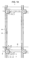
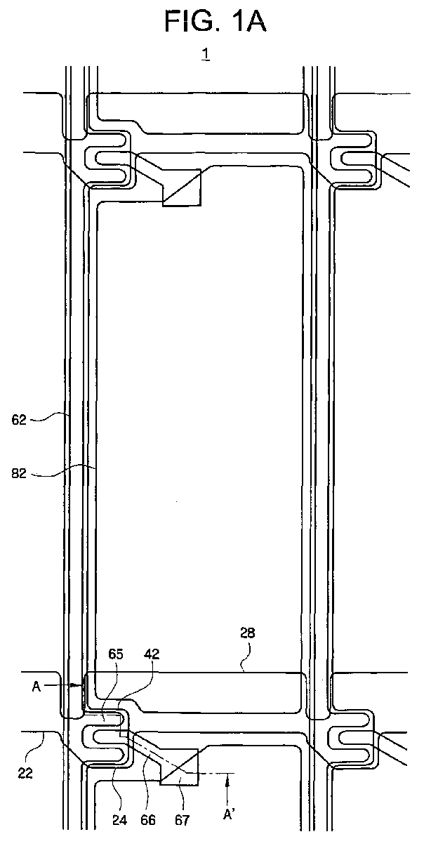
- FIG 1A is a layout view of the thin film transistor substrate according to the first embodiment of the present invention.
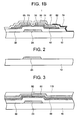
- FIG 1B is a sectional view of the thin film transistor substrate taken along the line A-A' of FIG 1A.
- a thin film transistor substrate 1 according to the first embodiment of the present invention is provided with gate wiring lines 22 and 24, a storage wiring line 28, a gate insulating layer pattern 32, an active layer pattern 42, ohmic contact layer patterns 55 and 56, data wiring lines 62, 65, 66, and 67, an overetched passivation layer pattern 74, and a pixel electrode 82 that are formed on an insulating substrate 10.
- the insulating substrate 10 may be made of a substance having desired levels of heat resistance and light transmission, such as transparent glass or plastics.
- the gate wiring lines 22 and 24 are formed on the insulating substrate 10 and extend in a first direction. Typically, the gate wiring lines 22, 24 are disposed parallel to a long side of the thin film transistor substrate 1.
- the gate wiring lines 22 and 24 include a plurality of gate lines 22 that transmits gate signals and gate electrodes 24 protruding from the gate lines 22.
- the gate electrode 24 constitutes three terminals of the thin film transistor in conjunction with a source electrode 65 and a drain electrode 66, which are described below.
- the storage wiring 28 may be formed by expanding a portion of the gate line 22.
- the storage wiring 28 is not limited to being made this way.
- it may be separated from the gate wiring lines 22, 24 in some embodiments.
- the shape of the storage wiring line 28 may vary, and the storage wiring line 28 may be omitted if necessary.
- the gate wiring lines 22 and 24, and the storage wiring line 28 may be made of an aluminum-based metal, such as aluminum (Al) and an aluminum alloy, a silver-based metal, such as silver (Ag) and a silver alloy, a copper-based metal, such as copper (Cu) and a copper alloy, a molybdenum-based metal, such as molybdenum (Mo) and a molybdenum alloy, chromium (Cr), titanium (Ti), or tantalum (Ta).
- the gate wiring lines 22 and 24, and the storage wiring line 28 may have a multilayered structure including two conductive layers having different physical properties (not shown).
- the gate wiring lines 22 and 24, and the storage wiring line 28 may be formed by applying PEDOT (PolyEthyleneDiOxyThiophene) that is a conductive organic polymer-based substance using a predetermined coating process, or by printing the conductive organic polymer-based substance using an inject-printing process.
- PEDOT PolyEthyleneDiOxyThiophene
- a gate insulating layer pattern 32 that is made of an inorganic insulating substance such as silicon oxide (SiOx) or silicon nitride (SiNx) or an organic insulating substance such as BCB (BenzoCycloButene), an acryl-based substance, or polyimide covers the gate wiring lines 22 and 24 and the storage wiring line 28 on the gate wiring lines 22 and 24 and the insulating substrate 10. That is, the gate insulating layer pattern 32 may be formed to expose a pixel region.
- an inorganic insulating substance such as silicon oxide (SiOx) or silicon nitride (SiNx) or an organic insulating substance such as BCB (BenzoCycloButene), an acryl-based substance, or polyimide
- the pixel region is defined by the gate wiring lines 22 and 24 and data wiring lines 62, 65, 66, and 67, and may be considered the region through which light emitted from a backlight assembly (not shown) passes in the liquid crystal display including the thin film transistor substrate 1.
- the active layer pattern 42 that is made of hydrogenated amorphous silicon, polysilicon, or the conductive organic substance is formed on an upper part of the gate insulating layer pattern 32.
- the active layer pattern 42 may have any suitable shape, and may be formed as an island or a stripe, for example.
- the active layer pattern may be provided under the data line 62 and extend to an upper part of the gate electrode 24.
- the active layer pattern 42 according to the present embodiment may substantially overlap all of the gate electrode and the data wiring lines 62, 65, 66, and 67 as described below. That is, the active layer pattern 42 may protrude from the source electrode 65 and the drain electrode 66.
- the shape of the active layer pattern 42 is not limited to the stripe, but may vary. In the case of when the active layer pattern 42 has an island shape, the active layer pattern 42 may be provided on the gate electrode 24 to overlap the gate electrode 24, and also overlap at least a portion of the source electrode 65 and the drain electrode 66.
- Ohmic contact layer patterns 55 and 56 that are made of silicide, n+ hydrogenated amorphous silicon in which an n-type impurity is doped at a high concentration, or ITO in which a p-type impurity is doped may be formed on the upper part of the active layer pattern 42.
- the ohmic contact layer patterns 55 and 56 are provided on the active layer pattern 42 to form a pair, and improves the contact characteristic between the source electrode 65 and the drain electrode 66 as described below, and the active layer pattern 42.
- the ohmic contact layer patterns 55 and 56 may be omitted.
- the data wiring lines 62, 65, 66, and 67 that include the data lines 62, the source electrode 65, the drain electrode 66, and a drain electrode expanded part 67 are formed on the ohmic contact layer patterns 55 and 56.
- the data lines 62 are disposed on the ohmic contact layer patterns 55 and 56 in a second direction.
- the second direction is substantially perpendicular to the first direction.
- a plurality of data lines is provided parallel to a short side of the thin film transistor substrate 1.
- the source electrodes 65 are connected to the data lines 62. A plurality of source electrodes 65 may be connected to the single data line 62. The source electrodes 65 face the drain electrodes 66 that are spaced apart from the source electrodes. The active layer pattern 42 is exposed in the area between the source electrode 65 and the drain electrode 66.
- the drain electrode 66 may include the drain electrode expanded part 67 that is formed by expanding an end of the drain electrode 66.
- the drain electrode expanded part 67 does not overlap the overetched passivation layer pattern 74 as described below, and is electrically connected directly to the pixel electrode 82. That is, the overetched passivation layer pattern 74 and the pixel electrode 82 may be formed on the same layer on the drain electrode expanded part 67.
- the drain electrode expanded part 67 is formed outside the pixel region to prevent an aperture ratio from being reduced.
- the data wiring lines 62, 65, 66, and 67 may be made of a refractory metal that has a high melting point, such as chromium, molybdenum-based metal, tantalum, and titanium. Additionally, the data wiring lines 62, 65, 66, and 67 may have a multilayered structure that includes a lower refractory metal layer (not shown) and an upper layer (not shown) which is made of a substance having low resistance and provided on the lower refractory metal layer.
- Examples of the multilayered structure may include a dual layer structure that has a lower chromium layer and an upper aluminum layer or a lower aluminum layer and an upper molybdenum layer, and a triple layer structure that has a molybdenum layer, an aluminum layer, and a molybdenum layer.
- the overetched passivation layer pattern 74 that is made of an organic insulating film is formed on the data wiring lines 62, 65, 66, and 67 and the exposed gate insulating layer pattern 32.
- the overetched passivation layer pattern 74 of the present embodiment includes two regions that are spaced apart from each other to expose at least a portion of the drain electrode 66, specifically, at least a portion of the drain electrode expanded part 67.
- the overetched passivation layer pattern 74 may not be formed in the pixel region through which light emitted from the backlight assembly passes.
- the overetched passivation layer pattern 74 is made of an inorganic substance that includes silicon nitride or silicon oxide, an organic substance that has excellent planarization property and photosensitivity, or a low dielectric insulating substance, such as a-Si:C:O or a-Si:O:F, that is formed using plasma enhanced chemical vapor deposition (PECVD). Additionally, the overetched passivation layer pattern 74 may have a dual layer structure including a lower inorganic layer and an upper organic layer in order to assure excellent property of the organic layer and to protect the exposed portion of the active layer pattern 42.
- PECVD plasma enhanced chemical vapor deposition
- the pixel electrode 82 may be formed in the pixel region of the insulating substrate 10, and is electrically directly connected to the drain electrode expanded part 67. That is, the overetched passivation layer pattern 74 may not be provided under the pixel electrode 82 while a portion of the ohmic contact layer pattern 56 and an end of the gate insulating layer pattern 32 that protrude from the drain electrode expanded part 67 are formed under the pixel electrode 82.
- the pixel electrode 82 of the present embodiment is made of a substance that includes zinc oxide.
- the pixel electrode 82 may be made of a substance that contains zinc oxide and one or more of Al 2 O 3 , AlF 3 , B 2 O 3 , Ga 2 O 3 , Y 2 O 3 , SiO 2 , SiO, TiO 2 , ZrO 3 , HfO 2 , and GeO 2 as an additive.
- the additive is selected in consideration of the desired resistance level and a current characteristic of the thin film transistor substrate 1.
- the pixel electrode 82 may include ZAO (aluminum doped zinc oxide). The step coverage of the ZAO is not very high.
- the pixel electrode 82 may be made of a transparent conductive substance such as ITO (Indium Tin Oxide) or IZO (Indium Zinc Oxide), or a reflective conductive substance such as copper (Cu) or silver (Ag).
- ITO Indium Tin Oxide
- IZO Indium Zinc Oxide
- Cu copper
- Au silver
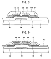
- FIGS. 2 to 13 are sectional views illustrating a method of producing a thin film transistor substrate according to the first embodiment of the present invention.
- gate wiring lines 22 and 24 that include a gate electrode 24, and a storage wiring line 28 are formed on an insulating substrate 10.
- a gate conductive layer is layered on the insulating substrate 10 using, for example, sputtering, and subjected to a photolithography process to form the gate line 22, the gate electrode 24, and the storage wiring line 28.
- a gate insulating layer 30, an active layer 40 that is made of hydrogenated amorphous silicon, and an ohmic contact layer 50 that is made of silicide, n+ hydrogenated amorphous silicon in which an n-type impurity is doped at a high concentration, or ITO in which a p-type impurity is doped are layered on the resulting structure.
- the gate insulating layer 30, the active layer 40, and the ohmic contact layer 50 may be layered using, for example, chemical vapor deposition (CVD).
- the conductive layer 60 for data wiring line is deposited on the ohmic contact layer 50 using, for example, sputtering, and a photoresist layer 110 is layered on the ohmic contact layer 50.
- the photoresist layer 110 is patterned to form photoresist patterns 112 and 114 for data wiring line on the conductive layer 60 for data wiring line.
- the photoresist patterns 112 and 114 for data wiring line include two regions having different thicknesses, and the photoresist pattern 114 for data wiring line having a large thickness covers regions in which the data line 62, the drain electrode expanded part 67, the source electrode 65, and the drain electrode 66 are formed.
- the photoresist pattern 112 for data wiring line having a small thickness covers the gap between the source electrode 65 and the drain electrode 66.
- the above-mentioned photoresist patterns 112 and 114 for data wiring line that include the regions having different thicknesses may be formed using a slit mask or a half tone mask, both of which are well known.
- the exposed conductive layer 60 for the data wiring line is etched using the photoresist patterns 112 and 114 as an etching mask.
- the etching of the conductive layer 60 for the data wiring line depends on the type and thickness of the conductive layer 60 that is used for the data wiring line.
- the conductive layer 60 for the data wiring line is subjected to wet etching.
- the conductive layer patterns 61 for the data lines 62 and the data wiring lines are formed.
- the patterns of the source electrode 65 and the drain electrode 66 of the channel region are not formed, and the conductive layer patterns 61 for the data wiring lines are not separated but form a single body in the channel region.
- formation of the conductive layer patterns 61 results in part of the active layer 40 to be exposed.
- the ohmic contact layer 50 and the active layer 40 provided under the ohmic contact layer are etched to form the incomplete ohmic contact layer pattern 51 and the incomplete active layer pattern 41 provided under the incomplete ohmic contact layer pattern 51.
- the ohmic contact layer 50 and the active layer 40 may be subjected to, for example, dry etching.
- the ohmic contact layer 50 and the active layer 40 are etched to expose the gate insulating layer 30.
- the photoresist pattern 112 for data wiring line having a small thickness is removed to expose the conductive layer pattern 61.
- the photoresist pattern 112 for a data wiring line having a small thickness may be removed by, for example, an ashing process using oxygen.
- the photoresist pattern 112 for the data wiring line having the small thickness of the photoresist patterns 112 and 114 may be removed in advance of etching the ohmic contact layer 50 and the active layer 40. In this case, the ashing process may be omitted.
- the exposed conductive layer pattern 61 for data wiring line of the channel region is etched using the photoresist pattern 114 for data wiring line having the large thickness as the etching mask.
- the source electrode 65, the drain electrode 66, and the drain electrode expanded part 67 are formed, and the incomplete ohmic contact layer pattern 51 is exposed in the area between the source electrode 65 and the drain electrode 66.
- the exposed portion of the incomplete ohmic contact layer pattern 51 is etched to perform separation.
- the production of the ohmic contact layer patterns 55 and 56 is finished.
- the incomplete active layer pattern 41 is exposed in the region in which the incomplete ohmic contact layer pattern 51 is etched. In this case, a portion of the incomplete active layer pattern 41 is etched to form the active layer pattern 42.
- a passivation layer 70 is layered on the resulting structure using, for example, CVD.
- a photoresist substance is applied to the passivation layer 70 and then patterned to form the photoresist patterns 122 and 124.
- the photoresist patterns 122 and 124 include a first region 122 and a second region 124.
- the first region 122 is formed on the portion of the passivation layer 70 provided on the data wiring lines 62, 65, and 66, but not on the portion of the passivation layer 70 and the drain electrode expanded part 67 provided on the gate wiring lines 22 and 24. Since the mask covers the first region 122, the first region 122 is not exposed, and the pixel region is exposed.
- the second region 124 Since the photoresist substance is exposed using, for example, the slit mask, the second region 124 has the thickness that is smaller than that of the first region 122.
- the second region 124 is formed on the portion of the passivation layer 70 provided on the active layer pattern 42 that protrudes from the drain electrode expanded part 67, and the portion of the passivation layer 70 provided on the gate insulating layer 30 that protrudes from the active layer pattern 42.
- the second region 124 may be formed on the portion of the passivation layer 70 provided on the storage wiring line 28.
- the second region 124 is spaced apart from the first region 122, and at least a portion of the passivation layer 70 that is provided on the drain electrode expanded part 67 is exposed in the gap between the first region 122 and the second region 124. Since the mask does not cover the gap between the first region and the second region, the gap is exposed to light during the exposure process.
- the exposed passivation layer 70 is subjected to first etching using the photoresist patterns 122 and 124 as the etching mask to form the passivation layer patterns 72.
- the etching of the passivation layer 70 is performed using a dry etching process.
- the passivation layer patterns 72 are spaced apart from each other to expose a portion of the drain electrode expanded part 67 provided under the photoresist patterns 122 and 124.
- the gate insulating layer 30 may be etched to form the gate insulating layer pattern 32. During the first etching, the overetching of the passivation layer 70 may not occur.
- Examples of an etching gas that is used during the first etching include CF 4 , SF 6 , CHF 3 , O 2 , or a mixture thereof.
- the etching rate may be controlled by adjusting the concentrations or proportions of the constituent elements.
- an etch back process is performed to remove the second region 124 using a stripper.
- the thickness of the first region 122 is reduced.
- the passivation layer pattern 72 is subjected to second etching using the first region 122 as the etching mask to form the overetched passivation layer pattern 74. Accordingly, an undercut is formed in the first region 122 so that the first region 122 protrudes from the overetched passivation layer pattern 74 and an area of the exposed drain electrode expanded part 67 is enlarged.
- the etching gas that is used during the second etching may be the same as the first etching gas.
- the first and the second etching gases may be different from each other in terms of the concentration or proportion of the constituent elements. It is preferable that the length of the first region 122 protruding from the overetched passivation layer pattern 74 be 3 ⁇ m or more so that a cut portion is formed during the application of a conductive substance for pixel electrodes (see reference numeral 80 of FIG 13) as described below.
- the drain electrode expanded part 67 and the insulating substrate 10 of the pixel region are exposed.
- a conductive substance for a pixel electrode 80 containing zinc oxide is layered on the whole surface of the resulting structure using a deposition process, such as sputtering.
- the conductive substance for pixel electrode 80 may be made of a substance that contains zinc oxide and one or more of Al 2 O 3 , AlF 3 , B 2 O 3 , Ga 2 O 3 , Y 2 O 3 , SiO 2 , SiO, TiO 2 , ZrO 3 , HfO 2 , and GeO 2 as an additive.
- the additive is selected in consideration of the desired resistance of the substance and a current characteristic of the thin film transistor substrate.
- Examples of the conductive substance for a pixel electrode 80 may include ZAO.
- ZAO may be deposited at a deposition pressure in the range of 0.3 to 3.0 Pa and a temperature in the range of 25 to 120°C to the thickness in the range of 10 to 200 nm. A portion of ZAO is layered on the first region 122 having a small thickness, and another portion of ZAO is layered on the structure that is not covered with the first region 122.
- the conductive substance for the pixel electrode 80 that is made of the ZAO has poor step coverage, the conductive substance for the pixel electrode 80 is not layered on an undercut region of the first region 122 and the overetched passivation layer pattern 74. That is, the conductive substance for the pixel electrode 80 that is layered on the first region 122 and the conductive substance for the pixel electrode 80 that is layered on the portion other than the first region 122 are not connected to each other and the cut portion is formed at an end of the first region 122.
- the portion of the conductive substance for the pixel electrode 80 includes the cut portion, efficiency of a subsequent lift off process may be improved. This results from the use of ZAO as the conductive substance for the pixel electrode 80. Lift off performance of ZAO will be described in detail.
- the first region 122 and the conductive substance for the pixel electrode 80 that is provided on the first region 122 are removed using the lift off process.
- a stripper that contains, for example, amines or glycols is injected to the above-mentioned cut portion by a spray process or a dip process to come into contact with the first region 122 of the photoresist patterns 122 and 124, the first region 122 is dissolved by the stripper to be separated from the overetched passivation layer pattern 74 and, at the same time, the conductive substance for the pixel electrode 80 that is made of ZAO and provided on the first region 122 is removed.
- the removal of the first region 122 and the conductive substance for pixel electrode 80 that is provided on the first region 122 depends on a contact time and a contact area between the first region 122 and the stripper, and the step coverage and the deposition temperature of the conductive substance for the pixel electrode 80.
- the lift off performance improves as the deposition temperature of the conductive substance for the pixel electrode 80 is reduced.
- the temperature of the chamber is reduced.
- most of the deposition devices are operated at high temperatures (for example, about 100°C), it is difficult to reduce the temperature of the devices. Accordingly, there is a need to find a conductive substance for the pixel electrode 80 that provides the desired level of lift-off performance even though the deposition is performed at the temperature that is almost the same as the operation temperature of the deposition chamber.
- the conductive substance for the pixel electrode 80 that can provide the desired level of lift-off performance may contain zinc oxide.
- the conductive substance for pixel electrode 80 may be made of a substance that contains zinc oxide and one or more of Al 2 O 3 , AlF 3 , B 2 O 3 , Ga 2 O 3 , Y 2 O 3 , SiO 2 , SiO, TiO 2 , ZrO 3 , HfO 2 , and GeO 2 as an additive.
- examples of the conductive substance for pixel electrode 80 include ZAO. The step coverage and the lift off performance of the conductive substance for pixel electrode 80 that includes the ZAO, and the current-voltage characteristic of the thin film transistor substrate 1 that is produced using the conductive substance for pixel electrode 80 will be described in detail.
- the first region 122 and the conductive substance for pixel electrode 80 that is provided on the first region 122 are removed to finish the production of the pixel electrode 82 that is formed directly on the insulating substrate 10 and comes directly into contact with the drain electrode expanded part 67.
- ZAO is used as the conductive substance for pixel electrode 80, and the pixel electrode 82 is formed using the lift-off process instead of patterning and etching to prevent a skew that may occur due to the high etching rate of ZAO.
- FIGS. 14 to 17 are sectional views illustrating a method of producing thin film transistor substrate according to the second embodiment of the present invention.
- the method of producing the thin film transistor substrate according to the second embodiment of the present invention is the same as the method according to the first embodiment of the present invention, with the exception of processes after the passivation layer 70 is formed on the insulating substrate 10.
- the first region 122 of the photoresist pattern is formed on the passivation layer 70.
- the second region (see reference numeral 124 of FIG 10) is not provided in the second embodiment. Since the first region 122 of the photoresist pattern of the second embodiment is substantially the same as the first region (see reference numeral 122 of FIG 10) of the first embodiment of the present invention, a description thereof is omitted.
- the exposed passivation layer 70 is etched using the first region 122 as the etching mask.
- an overetched passivation layer pattern 74' is formed.
- the undercut is formed in the first region 122 so that the first region 122 protrudes from the overetched passivation layer pattern 74'.
- the second etching is not performed, but the etching is performed once unlike the former embodiment. Therefore, examples of the etching gas may include CF 4 , SF 6 , CHF 3 , O 2 , and a mixture thereof.
- the etching rate may be controlled by adjusting the concentration or proportions of constituent elements to achieve the desired level of overetching.
- the ohmic contact layer patterns 55 and 56 of the active layer pattern 42 and the drain electrode 66 are etched by a single etching process to form an active layer pattern 42' and ohmic contact layer patterns 55' and 56'. Accordingly, an end of the drain electrode expanded part 67 protrudes on the sidewall between the overetched passivation layer pattern 74' and an ohmic contact layer 56'.
- the gate insulating layer 30 is patterned to form a gate insulating layer pattern 32'.
- the protruding drain electrode expanded part 67 is etched to form a deformed drain electrode expanded part 67'.
- the overetched passivation layer pattern 74', the deformed drain electrode expanded part 67', the ohmic contact layer patterns 55' and 56', and the active layer pattern 42' have inclined lateral surfaces.
- the lateral surface of the overetched passivation layer pattern 74' inclines at a different angle than the lateral surface of the deformed drain electrode expanded part 67', and the undercut of the first region 122 extends into the overetched passivation layer pattern 74'.
- the conductive substance for the pixel electrode 80 containing, for example, zinc oxide is layered on the whole surface of the resulting structure using a deposition process such as sputtering.
- a deposition process such as sputtering.
- the conductive substance for the pixel electrode 80 are the same as those of the former embodiment.
- a portion of the conductive substance for pixel electrode 80 is layered on the first region 122, and another portion of the conductive substance for pixel electrode 80 is layered on the exposed structure that is not covered with the first region 122. The two portions are not connected to each other, but cut due to poor step coverage of the conductive substance for the pixel electrode 80.
- the first region 122 and the conductive substance for pixel electrode 80 that is provided on the first region 122 are removed using the lift-off process.
- the lift-off process when a stripper is injected to the above-mentioned cut portion to separate the first region 122 from the overetched passivation layer pattern 74' and, at the same time, the conductive substance for the pixel electrode 80 that is provided on the first region 122 is removed. Accordingly, a pixel electrode 82' is formed.
- the lift-off performance is affected by the step coverage and the deposition temperature of the conductive substance for the pixel electrode 80.
- the lift off performance of ZAO that is used as the conductive substance for the pixel electrode 80 of the thin film transistor substrate that is produced according to the first embodiment and the second embodiment of the present invention will be compared to that of another conductive substance, and characteristics of the thin film transistor substrates that are produced according to the first embodiment and the modification of the first embodiment will be described with reference to FIGS. 18 to 21.
- FIGS. 1A, 1B, 13, 16, 17, and 18 stripper solubilities of ZAO and IZO that are used as the conductive substance for the pixel electrode 80 according to the first embodiment and the second embodiment of the present invention are compared to each other.
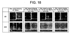
- FIG 18 schematically illustrates the stripper solubility of the conductive substance for the pixel electrode 80 that is used to produce the thin film transistor substrate according to the first embodiment of the present invention.
- the conductive substance for the pixel electrode 80 that is deposited on the upper surface of the first region 122 is removed by means of the lift off process using the stripper.
- the stripper that is used during the removal process is filtered and recycled through a stripper tank.
- the conductive substance for the pixel electrode 80 as well as the photoresist substance remains in the stripper. Accordingly, when the stripper is reused after the recycling, the conductive substance for the pixel electrode 80 remaining in the stripper may be deposited on the pixel region during the subsequent lift off process, thus forming defective pixels.
- the stripper solubility of the conductive substance for the pixel electrode 80 is chosen to be above a critical level.
- the stripper solubilities of ZAO and IZO that are used in the first embodiment and the second embodiment are compared to each other under the same condition. That is, the solubilities of ZAO and IZO in the stripper are compared to each other under four test conditions: (1) when stripping is performed using a typical lift off process for 140 sec, (2) when typical stripping is performed for 140 sec and the conductive substance for pixel electrode 80 is then dipped in the stripper for 1 min, (3) when typical stripping is performed for 140 sec and the conductive substance for pixel electrode 80 is then dipped in the stripper for 5 min, and (4) when typical stripping is performed for 140 sec and the conductive substance for pixel electrode 80 is then dipped in the stripper for 10 min.
- the lower portion is an insulating substrate and the upper portion is a pixel electrode 80 not stripped by a stripper.
- the solubility of ZAO in the stripper is better than that of IZO in the stripper under the four test conditions.
- test condition (3) since ZAO is dissolved in the stripper, after the lift-off process is performed using the stripper, all of the ZAO is dissolved while the stripper passes through the filter and the stripper tank.
- the production cost is reduced.
- FIGS. 1A, 1B, 13, 16, 17, 19, and 20 the step coverages and the lift-off performances of the conductive substances for the pixel electrode 80 that are used in the first embodiment and the second embodiment are compared.
- FIG 19 schematically illustrates the step coverage of the conductive substance for the pixel electrode that is used to produce the thin film transistor substrate according to the first embodiment of the present invention.
- FIG 20 schematically illustrates the lift-off performance of the conductive substance for the pixel electrode 80 that is used to produce the thin film transistor substrate according to the first embodiment of the present invention.
- the conductive substances for the pixel electrode 80 are deposited on the first region 122.
- the IZO is deposited at normal temperature, and the ZAO is deposited at 100°C.
- SEM scanning electron microscope
- plan views and sectional views of the observed surfaces are shown in FIG 19. From FIG 19, it can be seen that a difference in deposition characteristic of the IZO and the ZAO is insignificant in the plan views.
- the step coverage of the IZO that is indicated by the arrow and has the bright color is better than that of the ZAO.
- the step coverage is poorer in the case of low temperature deposition than in the case of high temperature deposition.
- the step coverage of ZAO is poorer than that of IZO.
- the lift off performance is reduced.
- the lift-off performances of both the conductive substances for the pixel electrode 80 that are deposited under the above-mentioned conditions are shown in FIG 20.
- the lift off performances of the IZO and the ZAO are compared with each other in the cases of when a stripping time is (1) 30 sec, (2) 60 sec, and (3) 50 sec + 50 sec.
- the left column shows the center of the insulating substrate 10
- the right column shows the first region 122 and the conductive substance for the pixel electrode 80 of the photoresist pattern that remains at an edge of the insulating substrate 10.
- FIG 20 shows that the lift-off performance of ZAO is better than that of IZO.
- the step coverage is poorer and the lift off performance is better in the case of the low temperature deposition of the conductive substance for the pixel electrode 80 in comparison with the case of the high temperature deposition. Accordingly, it can be seen that the lift-off performance of ZAO is better than that of IZO.
- ZAO is deposited at about 100°C, the deposition of ZAO may be performed without reducing the temperature of the chamber. Therefore, it is possible to avoid the delay caused by adjusting the chamber temperature and the associated cost.
- FIG 21 schematically illustrates the performance characteristics of the thin film transistor substrate that is produced using the method of producing the thin film transistor substrate according to the first embodiment of the present invention.
- the thin film transistor substrate (see reference numeral 1 of FIG 1B) that includes the ZAO as the conductive substance for the pixel electrode (see reference numeral 80 of FIGS. 13 and 16) and the thin film transistor substrate that includes the IZO as the conductive substance for the pixel electrode.
- the thin film transistor substrate in which the pixel electrode (see reference numeral 82 of FIG 1B and reference numeral 82' of FIG 17) is formed using the ZAO has a lower price and better lift-off performance than the thin film transistor substrate in which the pixel electrode is formed using IZO even though they have similar properties.
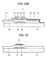
- FIG 22A is a layout view of the thin film transistor substrate according to the third embodiment of the present invention.
- FIG 22B is a sectional view of the thin film transistor substrate taken along the line B-B' of FIG 22A.
- the thin film transistor substrate according to the present embodiment has the same structure as the thin film transistor substrate 1 according to the former embodiment of the present invention, except that structures or positions of the active layer pattern 42", the data wiring lines 62", 65", 66", and 67", and the overetched passivation layer pattern 74" of the thin film transistor substrate 1" according to the present embodiment are different from those of the former embodiments.
- the active layer pattern 42" and the ohmic contact layer patterns 55" and 56" that are provided on the active layer pattern are formed as "islands.” That is, the active layer pattern 42" and the ohmic contact layer patterns 55" and 56" that are provided on the active layer pattern according to the present embodiment may overlap the gate electrode 24. Accordingly, the active layer pattern 42" and the ohmic contact layer patterns 55" and 56" that are provided on the active layer pattern may not be formed under the data line 62".
- the source electrode 65" and the drain electrode 66" are spaced apart from each other so they do not cover a portion of the ohmic contact layer patterns 55" and 56".
- the source electrode and the drain electrode are formed on the ohmic contact layer patterns 55" and 56" and the gate insulating layer pattern 32 so that the source electrode and the drain electrode do not overlap the entire ohmic contact layer patterns 55" and 56" but overlap a portion of the ohmic contact layer patterns. Meanwhile, the drain electrode expanded part 67" is formed on the gate insulating layer pattern 32".
- a portion of the overetched passivation layer pattern 74" is formed on the data wiring lines 62", 65", and 66" with the exception of the drain electrode expanded part 67", and another portion of the overetched passivation layer pattern 74" is formed on the gate insulating layer pattern 32"overetched passivation layer pattern 74.
- the pixel electrode 82" may be formed directly on the insulating substrate 10 in the pixel region, and cover an upper part of the overetched passivation layer pattern 74" and the drain electrode expanded part 67" that are formed on the gate insulating layer pattern 32.
- the pixel electrode 82" according to the present embodiment contains zinc oxide, and examples of the pixel electrode are the same as those of the former embodiment.
- FIGS. 23 to 29 are sectional views illustrating the steps of a method of producing a thin film transistor substrate according to the third embodiment of the present invention.
- the gate wiring lines 22 and 24 that include the gate line 22 and the gate electrode 24, and the storage wiring line 28 are formed on the insulating substrate 10.
- the gate insulating layer 30 made of silicon nitride, an intrinsic amorphous silicon layer, and a doped amorphous silicon layer are sequentially deposited on the resulting structure using, for example, a chemical vapor deposition process, to the thickness of 150 to 500 nm, 50 to 200 nm, and 30 to 60 nm, respectively.
- the intrinsic amorphous silicon layer and the doped amorphous silicon layer are subjected to a photolithography process to form an island-type active layer pattern 42" and incomplete ohmic contact layer pattern 51" on the gate insulating layer 30 provided on the upper part of the gate electrode 24.
- the active layer pattern 42" according to the present embodiment does not protrude from the data wiring lines 62", 65", 66", and 67". Therefore, stability is assured.
- the data wiring lines 62", 65", 66", and 67" include the data line 62" that extends perpendicularly to the gate line 22, the source electrode 65" that is connected to the data line 62" and extends to the upper part of the gate electrode 24, the drain electrode 66" that is separated from the source electrode 65” and is located across the gate electrode 24 from the source electrode 65", and the drain electrode 66", and the drain electrode expanded part 67" that extends from the drain electrode 66" to overlap the storage wiring line 28 and has a large area.
- the incomplete ohmic contact layer 51" that is not covered with the data wiring lines 62", 65", 66", and 67" is etched to form the ohmic contact layer patterns 55" and 56" and to expose the active layer pattern 42" between the ohmic contact layer patterns 55" and 56".
- an oxygen plasma process be performed in order to stabilize the exposed surface of the active layer pattern 42".
- a passivation layer 70" is formed on the resulting structure.
- a photoresist substance is applied on the passivation layer 70" and patterned to form the photoresist patterns 122 and 124.
- the photoresist patterns 122 and 124 include the first region 122 and the second region 124 that is spaced apart from the first region 122.
- the second region 124 is thinner than the first region 122.
- the positions and the formation methods of the first and the second regions 122, 124 are the same as those of the former embodiment.
- the passivation layer 70" that is exposed using the photoresist patterns 122 and 124 as the etching mask is subjected to first etching to form the passivation layer pattern 72".
- the type of the etching gas that is used to form the passivation layer pattern 72" and the position of the passivation layer pattern 72" are the same as those of the former embodiment, and the overetching of the passivation layer pattern 72" does not occur.
- an etch-back process is performed to remove the second region 124 using the stripper, thereby reducing the thickness of the first region 122.
- the passivation layer pattern 72" is subjected to a second etching using the first region 122 having a reduced thickness as the etching mask to form the overetched passivation layer pattern 74". Accordingly, the undercut is formed in the first region 122 so that the first region 122 protrudes from the overetched passivation layer pattern 74".
- the exposed area of the drain electrode expanded part 67" is increased.
- the composition of the etching gas is controlled so that the overetched passivation layer pattern 74" is capable of being formed.
- the source electrode 55", the drain electrode 56", and the drain electrode expanded part 67" cover the active layer pattern 42" and the ohmic contact layer patterns 55" and 56"
- the active layer pattern 42" and the ohmic contact layer patterns 55" and 56" are not etched during the first and the second etching processes of the present embodiment unlike the first embodiment of the present invention.
- the conductive substance for the pixel electrode 80 is layered on the resulting structure using a deposition process such as a sputtering process.
- the deposition condition is the same as that of the former embodiment.
- the conductive substance for the pixel electrode 80 that is used has poor step coverage, the conductive substance for the pixel electrode 80 is not layered but the cut portion is formed on the undercut portion of the first region 122 and the overetched passivation layer pattern 74".
- the first region 122 and the conductive substance for the pixel electrode 80 that is provided on the first region 122 are removed using the lift-off process to form the pixel electrode 82".
- the stripper is injected into the cut portion of the layer in which the conductive substance for the pixel electrode 80 is formed to separate the first region 122 from the overetched passivation layer pattern 74" and to remove the conductive substance for the pixel electrode 80 provided on the first region like the former embodiment.
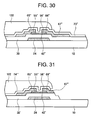
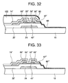
- FIGS. 30 to 33 are sectional views illustrating a method of producing a thin film transistor substrate according to a fourth embodiment of the present invention.
- the method of producing the thin film transistor substrate according to the fourth embodiment is the same as the method according to the third embodiment of the present invention, with the exception of the processes after the passivation layer 70" that is formed on the insulating substrate 10.
- the first region 122 of the photoresist pattern is formed on the passivation layer 70".
- the exposed passivation layer 70" is etched once using the first region 122 as the etching mask.
- an overetched passivation layer pattern 74′′′ is formed.
- the undercut is formed in the first region 122 so that the first region 122 protrudes from the overetched passivation layer pattern 74"'. That is, in the fourth embodiment, there is only one etching step. Accordingly, the composition of the etching gas is controlled to achieve the desired level of overetching.
- an end of the drain electrode expanded part 67" protrudes from the overetched passivation layer pattern 74"'.
- the gate insulating layer 30 is patterned to form the gate insulating layer pattern 32' during the etching. Meanwhile, since the source electrode 55", the drain electrode 56", and the drain electrode expanded part 67" cover the active layer pattern 42" and the ohmic contact layer patterns 55" and 56", the active layer pattern 42" and the ohmic contact layer patterns 55" and 56" are not etched during the etching process, unlike in the first embodiment of the present invention.
- the conductive substance for the pixel electrode 80 is layered on the entire surface of the resulting structure using a deposition process such as sputtering.
- the conductive substance for pixel electrode 80 contains zinc oxides, and preferable examples of the conductive substance for the pixel electrode are the same as those of the third embodiment.
- a portion of the conductive substance for the pixel electrode 80 is layered on the first region 122, and another portion of the conductive substance for the pixel electrode 80 is layered on the exposed structure that is not covered with the first region 122.
- the two portions are not connected to each other, but cut due to poor step coverage of the conductive substance for pixel electrode 80.
- the first region 122 and the conductive substance for pixel electrode 80 that is provided on the first region 122 are removed using the lift-off process.
- a pixel electrode 82''' is formed.
- the lift-off process and the lift-off performance are the same as those of the third embodiment.
- the thin film transistor substrates and the methods of producing the thin film transistor substrates according to the embodiments and the modifications of the present invention have one or more following advantages.
- the pixel electrode that includes low-priced zinc oxide is provided, it is possible to reduce the production cost of the thin film transistor substrate.
- the lift-off process is applied using the strip of the conductive substance for the pixel electrode that includes zinc oxide, it is possible to easily form the thin film transistor substrate.
- the conductive substance for the pixel electrode that contains zinc oxide is easily dissolved in the stripper, it is possible to improve a life of a filter when the stripper is reused and to prevent the formation of defective pixels where the conductive substance for the pixel electrode is attached to the pixel region.
Landscapes
- Physics & Mathematics (AREA)
- Nonlinear Science (AREA)
- Engineering & Computer Science (AREA)
- Microelectronics & Electronic Packaging (AREA)
- Mathematical Physics (AREA)
- Chemical & Material Sciences (AREA)
- Crystallography & Structural Chemistry (AREA)
- General Physics & Mathematics (AREA)
- Optics & Photonics (AREA)
- Thin Film Transistor (AREA)
- Liquid Crystal (AREA)
Abstract
Description
- The present invention relates to a thin film transistor substrate and a method of producing the same and, more particularly, to a thin film transistor substrate that has reduced production cost and defect rate and a method of producing the same pixel electrode.
- A liquid crystal display includes two substrates and a liquid crystal layer that is interposed between the two substrates. One of the two substrates is a thin film transistor substrate. In the thin film transistor substrate, a plurality of wiring lines is formed on an insulating substrate. A representative example of a process of forming wiring lines includes a photolithography process in which constituent substances are layered and patterned using a mask process. However, since the photolithography process includes numerous processes such as deposition of thin film, application of a photoresist, alignment of a mask, exposing, developing, etching, and stripping, the process time is long and product cost is high.
- A lift-off process has been used to reduce the number of mask processes. In a lift-off process, when a passivation layer and a pixel electrode of a thin film transistor substrate are used, the passivation layer is patterned using a photoresist pattern, a conductive substance is layered on the entire substrate surface, and the photoresist pattern and some of the conductive substance for the pixel electrode that is provided on the photoresist pattern are simultaneously removed using a stripper to form the pixel electrode.
- To remove the photoresist pattern and an upper surface that is coated with the conductive substance, the stripper is brought into contact with a lateral surface or a lower surface of the photoresist pattern. In connection with this, a contact area of the stripper and the photoresist pattern must be large enough to prevent the formation of unacceptable patterns resulting from the remaining photoresist pattern. That is, it is required that the passivation layer, which is provided under the photoresist pattern, be overetched to form desirable undercuts in the photoresist pattern. It is also required that step coverage of the conductive substance for the pixel electrode, which is provided on the photoresist pattern, is not very high. Meanwhile, in the lift-off process, since the stripper is frequently reused, defects may form on the thin film transistor substrate when the conductive substance for the pixel electrode remains in the stripper undissolved. In addition, since the conductive substance for the pixel electrode is removed during the lift-off process, reduction in the production cost of the thin film transistor substrate may be affected.
- Accordingly, there remains a need to develop a thin film transistor substrate using a conductive substance for a pixel electrode that has desirable step coverage, and can desirably dissolve in a stripper to improve the lift off performance at a reduced cost.
- The present invention provides a thin film transistor substrate that has reduced production cost and defect rate. The present invention is also provides a method of producing the thin film transistor substrate.
- According to one aspect, the present invention is a thin film transistor substrate including a gate wiring line formed on an insulating substrate and including a gate electrode, a data wiring line formed on the gate wiring line and including a source electrode and a drain electrode, a passivation layer pattern formed on the data wiring line except on a part of the drain electrode and a pixel region, and a pixel electrode electrically connected to the drain electrode and including zinc oxide.
- According to another aspect, the present invention is a thin film transistor substrate including a gate wiring line formed on an insulating substrate and including a gate electrode, a data wiring line formed on the gate wiring line and including a source electrode and a drain electrode, a passivation layer pattern formed on the data wiring line except on a part of the drain electrode and a pixel region, and a pixel electrode electrically connected to the drain electrode, contacting the insulating substrate and including zinc oxide.
- According to still another aspect, the present invention is a method of producing a thin film transistor substrate. The method includes forming a gate wiring line including a gate electrode on an insulating substrate, forming a data wiring line including a source electrode and a drain electrode on the gate wiring line, forming a passivation layer pattern on the data wiring line except for a part of the drain electrode and a pixel region, and forming a pixel electrode electrically connected to the drain electrode. The pixel electrode includes zinc oxide.
- The above and other features and advantages of the present invention will become more apparent by describing in detail preferred embodiments thereof with reference to the attached drawings, in which:
- FIG 1A is a layout view of a thin film transistor substrate according to a first embodiment of the present invention;
- FIG 1B is a sectional view of the thin film transistor substrate taken along the line A-A' of FIG 1A;
- FIGS. 2 to 13 are sectional views illustrating a method of producing a thin film transistor substrate according to the first embodiment of the present invention;
- FIGS. 14 to 17 are sectional views illustrating a method of producing a thin film transistor substrate according to a second embodiment of the present invention;
- FIG 18 schematically illustrates solubility of a conductive substance for a pixel electrode in a stripper, wherein the conductive substance is used to produce the thin film transistor substrate according to the first embodiment of the present invention;
- FIG 19 schematically illustrates the step coverage of the conductive substance for the pixel electrode that is used to produce the thin film transistor substrate according to the first embodiment of the present invention;
- FIG 20 schematically illustrates lift-off performance of the conductive substance for the pixel electrode that is used to produce the thin film transistor substrate according to the first embodiment of the present invention;
- FIG 21 schematically illustrates the performance characteristics of the thin film transistor substrate that is produced using a method according to the first embodiment of the present invention;
- FIG 22A is a layout view of a thin film transistor substrate according to a third embodiment of the present invention;
- FIG 22B is a sectional view of the thin film transistor substrate taken along the line B-B' of FIG. 22A;
- FIGS. 23 to 29 are sectional views illustrating a method of producing a thin film transistor substrate according to the third embodiment of the present invention; and
- FIGS. 30 to 33 are sectional views illustrating a method of producing a thin film transistor substrate according to modification of the third embodiment of the present invention.
- Advantages and features of the present invention and methods of accomplishing the same may be understood more readily by reference to the following detailed description of preferred embodiments and the accompanying drawings. The present invention may, however, be embodied in many different forms and should not be construed as being limited to the embodiments set forth herein. Rather, these embodiments are provided so that this disclosure will be thorough and complete and will fully convey the concept of the invention to those skilled in the art. The present invention will be defined by the appended claims. Like reference numerals refer to like elements throughout the specification.
- It will be understood that when an element or layer is referred to as being "on" on "connected to" another element or layer, it can be in contact with the other element or layer or intervening elements or layers may be present. In contrast, when an element is referred to as being "directly on" or "directly connected to" another element or layer, there are no intervening elements or layers present. Like reference numerals refer to like elements throughout the specification.
- Spatially relative terms, such as "below", "beneath", "lower", "above", "upper" and the like, may be used herein for ease of description to describe one element or feature's relationship to another element(s) or feature(s) as illustrated in the figures. It will be understood that the spatially relative terms are intended to encompass different orientations of the device in use or operation in addition to the orientation depicted in the figures. Like reference numerals refer to like elements throughout the specification.
- Hereinafter, embodiments of the present invention will be described in detail with reference to the accompanying drawings.
- A thin film transistor substrate according to a first embodiment of the present invention will be described in detail with reference to FIGS. 1A and 1B. FIG 1A is a layout view of the thin film transistor substrate according to the first embodiment of the present invention. FIG 1B is a sectional view of the thin film transistor substrate taken along the line A-A' of FIG 1A.
- A thin
film transistor substrate 1 according to the first embodiment of the present invention is provided withgate wiring lines storage wiring line 28, a gateinsulating layer pattern 32, anactive layer pattern 42, ohmiccontact layer patterns data wiring lines passivation layer pattern 74, and apixel electrode 82 that are formed on aninsulating substrate 10. - The
insulating substrate 10 may be made of a substance having desired levels of heat resistance and light transmission, such as transparent glass or plastics. - The
gate wiring lines insulating substrate 10 and extend in a first direction. Typically, thegate wiring lines film transistor substrate 1. - The
gate wiring lines gate lines 22 that transmits gate signals andgate electrodes 24 protruding from thegate lines 22. Thegate electrode 24 constitutes three terminals of the thin film transistor in conjunction with asource electrode 65 and adrain electrode 66, which are described below. - The
storage wiring 28 may be formed by expanding a portion of thegate line 22. However, thestorage wiring 28 is not limited to being made this way. For example, it may be separated from thegate wiring lines storage wiring line 28 may vary, and thestorage wiring line 28 may be omitted if necessary. - The
gate wiring lines storage wiring line 28 may be made of an aluminum-based metal, such as aluminum (Al) and an aluminum alloy, a silver-based metal, such as silver (Ag) and a silver alloy, a copper-based metal, such as copper (Cu) and a copper alloy, a molybdenum-based metal, such as molybdenum (Mo) and a molybdenum alloy, chromium (Cr), titanium (Ti), or tantalum (Ta). In addition, thegate wiring lines storage wiring line 28 may have a multilayered structure including two conductive layers having different physical properties (not shown). Meanwhile, thegate wiring lines storage wiring line 28 may be formed by applying PEDOT (PolyEthyleneDiOxyThiophene) that is a conductive organic polymer-based substance using a predetermined coating process, or by printing the conductive organic polymer-based substance using an inject-printing process. - A gate insulating
layer pattern 32 that is made of an inorganic insulating substance such as silicon oxide (SiOx) or silicon nitride (SiNx) or an organic insulating substance such as BCB (BenzoCycloButene), an acryl-based substance, or polyimide covers thegate wiring lines storage wiring line 28 on thegate wiring lines substrate 10. That is, the gate insulatinglayer pattern 32 may be formed to expose a pixel region. In connection with this, the pixel region is defined by thegate wiring lines data wiring lines film transistor substrate 1. - The
active layer pattern 42 that is made of hydrogenated amorphous silicon, polysilicon, or the conductive organic substance is formed on an upper part of the gate insulatinglayer pattern 32. - The
active layer pattern 42 may have any suitable shape, and may be formed as an island or a stripe, for example. When the active layer pattern has the stripe shape as shown in the present embodiment, the active layer pattern may be provided under thedata line 62 and extend to an upper part of thegate electrode 24. Theactive layer pattern 42 according to the present embodiment may substantially overlap all of the gate electrode and thedata wiring lines active layer pattern 42 may protrude from thesource electrode 65 and thedrain electrode 66. However, the shape of theactive layer pattern 42 is not limited to the stripe, but may vary. In the case of when theactive layer pattern 42 has an island shape, theactive layer pattern 42 may be provided on thegate electrode 24 to overlap thegate electrode 24, and also overlap at least a portion of thesource electrode 65 and thedrain electrode 66. - Ohmic
contact layer patterns active layer pattern 42. The ohmiccontact layer patterns active layer pattern 42 to form a pair, and improves the contact characteristic between thesource electrode 65 and thedrain electrode 66 as described below, and theactive layer pattern 42. When the contact characteristic between theactive layer pattern 42 and thesource electrode 65 and thedrain electrode 66 that are provided on the upper part of theactive layer pattern 42 is acceptable, the ohmiccontact layer patterns - The
data wiring lines source electrode 65, thedrain electrode 66, and a drain electrode expandedpart 67 are formed on the ohmiccontact layer patterns - The data lines 62 are disposed on the ohmic
contact layer patterns film transistor substrate 1. - The
source electrodes 65 are connected to the data lines 62. A plurality ofsource electrodes 65 may be connected to thesingle data line 62. Thesource electrodes 65 face thedrain electrodes 66 that are spaced apart from the source electrodes. Theactive layer pattern 42 is exposed in the area between thesource electrode 65 and thedrain electrode 66. - The
drain electrode 66 may include the drain electrode expandedpart 67 that is formed by expanding an end of thedrain electrode 66. In the present embodiment, at least a portion of the drain electrode expandedpart 67 does not overlap the overetchedpassivation layer pattern 74 as described below, and is electrically connected directly to thepixel electrode 82. That is, the overetchedpassivation layer pattern 74 and thepixel electrode 82 may be formed on the same layer on the drain electrode expandedpart 67. - The drain electrode expanded
part 67 is formed outside the pixel region to prevent an aperture ratio from being reduced. - The
data wiring lines data wiring lines - The overetched
passivation layer pattern 74 that is made of an organic insulating film is formed on thedata wiring lines layer pattern 32. The overetchedpassivation layer pattern 74 of the present embodiment includes two regions that are spaced apart from each other to expose at least a portion of thedrain electrode 66, specifically, at least a portion of the drain electrode expandedpart 67. The overetchedpassivation layer pattern 74 may not be formed in the pixel region through which light emitted from the backlight assembly passes. In connection with this, the overetchedpassivation layer pattern 74 is made of an inorganic substance that includes silicon nitride or silicon oxide, an organic substance that has excellent planarization property and photosensitivity, or a low dielectric insulating substance, such as a-Si:C:O or a-Si:O:F, that is formed using plasma enhanced chemical vapor deposition (PECVD). Additionally, the overetchedpassivation layer pattern 74 may have a dual layer structure including a lower inorganic layer and an upper organic layer in order to assure excellent property of the organic layer and to protect the exposed portion of theactive layer pattern 42. - The
pixel electrode 82 may be formed in the pixel region of the insulatingsubstrate 10, and is electrically directly connected to the drain electrode expandedpart 67. That is, the overetchedpassivation layer pattern 74 may not be provided under thepixel electrode 82 while a portion of the ohmiccontact layer pattern 56 and an end of the gate insulatinglayer pattern 32 that protrude from the drain electrode expandedpart 67 are formed under thepixel electrode 82. - The
pixel electrode 82 of the present embodiment is made of a substance that includes zinc oxide. To be more specific, thepixel electrode 82 may be made of a substance that contains zinc oxide and one or more of Al2O3, AlF3, B2O3, Ga2O3, Y2O3, SiO2, SiO, TiO2, ZrO3, HfO2, and GeO2 as an additive. The additive is selected in consideration of the desired resistance level and a current characteristic of the thinfilm transistor substrate 1. Thepixel electrode 82 may include ZAO (aluminum doped zinc oxide). The step coverage of the ZAO is not very high. Accordingly, it is easy to form thepixel electrode 82 having the structure shown in the present embodiment using ZAO, and it is possible to reduce the production cost of the thinfilm transistor substrate 1 due to the low-priced ZAO. Thepixel electrode 82 may be made of a transparent conductive substance such as ITO (Indium Tin Oxide) or IZO (Indium Zinc Oxide), or a reflective conductive substance such as copper (Cu) or silver (Ag). When ZAO is used, the production cost of the thinfilm transistor substrate 1 is reduced significantly but the current-voltage characteristic is not lower than when ITO is used. - Hereinafter, a method of producing the thin film transistor substrate according to the first embodiment of the present invention will be described in detail with reference to FIGS. 1A, 1B, and 2 to 13. FIGS. 2 to 13 are sectional views illustrating a method of producing a thin film transistor substrate according to the first embodiment of the present invention.
- First, with reference to FIGS. 1A and 2,
gate wiring lines gate electrode 24, and astorage wiring line 28 are formed on an insulatingsubstrate 10. To be more specific, a gate conductive layer is layered on the insulatingsubstrate 10 using, for example, sputtering, and subjected to a photolithography process to form thegate line 22, thegate electrode 24, and thestorage wiring line 28. - Subsequently, with reference to FIGS. 3 and 1A, a
gate insulating layer 30, anactive layer 40 that is made of hydrogenated amorphous silicon, and anohmic contact layer 50 that is made of silicide, n+ hydrogenated amorphous silicon in which an n-type impurity is doped at a high concentration, or ITO in which a p-type impurity is doped, are layered on the resulting structure. Thegate insulating layer 30, theactive layer 40, and theohmic contact layer 50 may be layered using, for example, chemical vapor deposition (CVD). - Subsequently, the
conductive layer 60 for data wiring line is deposited on theohmic contact layer 50 using, for example, sputtering, and aphotoresist layer 110 is layered on theohmic contact layer 50. - Subsequently, with reference to FIGS. 3, 4, and 1A, the
photoresist layer 110 is patterned to formphotoresist patterns conductive layer 60 for data wiring line. Thephotoresist patterns photoresist pattern 114 for data wiring line having a large thickness covers regions in which thedata line 62, the drain electrode expandedpart 67, thesource electrode 65, and thedrain electrode 66 are formed. Thephotoresist pattern 112 for data wiring line having a small thickness covers the gap between thesource electrode 65 and thedrain electrode 66. The above-mentionedphotoresist patterns - Subsequently, with reference to FIGS. 1A, 4, and 5, the exposed
conductive layer 60 for the data wiring line is etched using thephotoresist patterns conductive layer 60 for the data wiring line depends on the type and thickness of theconductive layer 60 that is used for the data wiring line. Preferably, theconductive layer 60 for the data wiring line is subjected to wet etching. As a result, theconductive layer patterns 61 for the data lines 62 and the data wiring lines are formed. At this point, the patterns of thesource electrode 65 and thedrain electrode 66 of the channel region are not formed, and theconductive layer patterns 61 for the data wiring lines are not separated but form a single body in the channel region. - As shown in FIG 5, formation of the
conductive layer patterns 61 results in part of theactive layer 40 to be exposed. As shown in FIGS. 1A, 5, and 6, theohmic contact layer 50 and theactive layer 40 provided under the ohmic contact layer are etched to form the incomplete ohmiccontact layer pattern 51 and the incompleteactive layer pattern 41 provided under the incomplete ohmiccontact layer pattern 51. Theohmic contact layer 50 and theactive layer 40 may be subjected to, for example, dry etching. Theohmic contact layer 50 and theactive layer 40 are etched to expose thegate insulating layer 30. - Subsequently, with reference to FIGS. 1A, 6, and 7, among the
photoresist patterns photoresist pattern 112 for data wiring line having a small thickness is removed to expose theconductive layer pattern 61. Thephotoresist pattern 112 for a data wiring line having a small thickness may be removed by, for example, an ashing process using oxygen. Thephotoresist pattern 112 for the data wiring line having the small thickness of thephotoresist patterns ohmic contact layer 50 and theactive layer 40. In this case, the ashing process may be omitted. - Subsequently, with reference to FIGS. 1A, 7, and 8, the exposed
conductive layer pattern 61 for data wiring line of the channel region is etched using thephotoresist pattern 114 for data wiring line having the large thickness as the etching mask. As a result, thesource electrode 65, thedrain electrode 66, and the drain electrode expandedpart 67 are formed, and the incomplete ohmiccontact layer pattern 51 is exposed in the area between thesource electrode 65 and thedrain electrode 66. Subsequently, the exposed portion of the incomplete ohmiccontact layer pattern 51 is etched to perform separation. As a result, the production of the ohmiccontact layer patterns active layer pattern 41 is exposed in the region in which the incomplete ohmiccontact layer pattern 51 is etched. In this case, a portion of the incompleteactive layer pattern 41 is etched to form theactive layer pattern 42. - Subsequently, with reference to FIG 9, a
passivation layer 70 is layered on the resulting structure using, for example, CVD. - Subsequently, with reference to FIGS. 1A and 10, a photoresist substance is applied to the
passivation layer 70 and then patterned to form thephotoresist patterns photoresist patterns first region 122 and asecond region 124. Thefirst region 122 is formed on the portion of thepassivation layer 70 provided on thedata wiring lines passivation layer 70 and the drain electrode expandedpart 67 provided on thegate wiring lines first region 122, thefirst region 122 is not exposed, and the pixel region is exposed. Since the photoresist substance is exposed using, for example, the slit mask, thesecond region 124 has the thickness that is smaller than that of thefirst region 122. Thesecond region 124 is formed on the portion of thepassivation layer 70 provided on theactive layer pattern 42 that protrudes from the drain electrode expandedpart 67, and the portion of thepassivation layer 70 provided on thegate insulating layer 30 that protrudes from theactive layer pattern 42. In addition, thesecond region 124 may be formed on the portion of thepassivation layer 70 provided on thestorage wiring line 28. Thesecond region 124 is spaced apart from thefirst region 122, and at least a portion of thepassivation layer 70 that is provided on the drain electrode expandedpart 67 is exposed in the gap between thefirst region 122 and thesecond region 124. Since the mask does not cover the gap between the first region and the second region, the gap is exposed to light during the exposure process. - Subsequently, with reference to FIGS. 10 and 11, the exposed
passivation layer 70 is subjected to first etching using thephotoresist patterns passivation layer patterns 72. The etching of thepassivation layer 70 is performed using a dry etching process. Thepassivation layer patterns 72 are spaced apart from each other to expose a portion of the drain electrode expandedpart 67 provided under thephotoresist patterns gate insulating layer 30 may be etched to form the gate insulatinglayer pattern 32. During the first etching, the overetching of thepassivation layer 70 may not occur. Examples of an etching gas that is used during the first etching include CF4, SF6, CHF3, O2, or a mixture thereof. The etching rate may be controlled by adjusting the concentrations or proportions of the constituent elements. - Subsequently, with reference to FIGS. 11 and 12, an etch back process is performed to remove the
second region 124 using a stripper. In this case, the thickness of thefirst region 122 is reduced. Next, thepassivation layer pattern 72 is subjected to second etching using thefirst region 122 as the etching mask to form the overetchedpassivation layer pattern 74. Accordingly, an undercut is formed in thefirst region 122 so that thefirst region 122 protrudes from the overetchedpassivation layer pattern 74 and an area of the exposed drain electrode expandedpart 67 is enlarged. In this case, the etching gas that is used during the second etching may be the same as the first etching gas. Alternatively, the first and the second etching gases may be different from each other in terms of the concentration or proportion of the constituent elements. It is preferable that the length of thefirst region 122 protruding from the overetchedpassivation layer pattern 74 be 3 µm or more so that a cut portion is formed during the application of a conductive substance for pixel electrodes (seereference numeral 80 of FIG 13) as described below. - After the first etching and the second etching are performed, the drain electrode expanded
part 67 and the insulatingsubstrate 10 of the pixel region are exposed. - Subsequently, with reference to FIGS. 1A, 12, 13, for example, a conductive substance for a
pixel electrode 80 containing zinc oxide is layered on the whole surface of the resulting structure using a deposition process, such as sputtering. To be more specific, the conductive substance forpixel electrode 80 may be made of a substance that contains zinc oxide and one or more of Al2O3, AlF3, B2O3, Ga2O3, Y2O3, SiO2, SiO, TiO2, ZrO3, HfO2, and GeO2 as an additive. The additive is selected in consideration of the desired resistance of the substance and a current characteristic of the thin film transistor substrate. Examples of the conductive substance for apixel electrode 80 may include ZAO. In the case of when the ZAO is used as the conductive substance forpixel electrode 80, ZAO may be deposited at a deposition pressure in the range of 0.3 to 3.0 Pa and a temperature in the range of 25 to 120°C to the thickness in the range of 10 to 200 nm. A portion of ZAO is layered on thefirst region 122 having a small thickness, and another portion of ZAO is layered on the structure that is not covered with thefirst region 122. In this case, since the conductive substance for thepixel electrode 80 that is made of the ZAO has poor step coverage, the conductive substance for thepixel electrode 80 is not layered on an undercut region of thefirst region 122 and the overetchedpassivation layer pattern 74. That is, the conductive substance for thepixel electrode 80 that is layered on thefirst region 122 and the conductive substance for thepixel electrode 80 that is layered on the portion other than thefirst region 122 are not connected to each other and the cut portion is formed at an end of thefirst region 122. As described above, since the portion of the conductive substance for thepixel electrode 80 includes the cut portion, efficiency of a subsequent lift off process may be improved. This results from the use of ZAO as the conductive substance for thepixel electrode 80. Lift off performance of ZAO will be described in detail. - Subsequently, with reference to FIGS. 1A, 1B, and 13, the
first region 122 and the conductive substance for thepixel electrode 80 that is provided on thefirst region 122 are removed using the lift off process. To be more specific, when a stripper that contains, for example, amines or glycols, is injected to the above-mentioned cut portion by a spray process or a dip process to come into contact with thefirst region 122 of thephotoresist patterns first region 122 is dissolved by the stripper to be separated from the overetchedpassivation layer pattern 74 and, at the same time, the conductive substance for thepixel electrode 80 that is made of ZAO and provided on thefirst region 122 is removed. - In connection with this, the removal of the
first region 122 and the conductive substance forpixel electrode 80 that is provided on thefirst region 122 depends on a contact time and a contact area between thefirst region 122 and the stripper, and the step coverage and the deposition temperature of the conductive substance for thepixel electrode 80. Through the above-mentioned description, it can be understood that when the width of the undercut portion of thefirst region 122 which is formed by the overetchedpassivation layer pattern 74 under thefirst region 122 is not changed, the removal of thefirst region 122 and the conductive substance for thepixel electrode 80 provided on thefirst region 122 which depends on the step coverage of the conductive substance for thepixel electrode 80, that is, the lift off performance, is excellent. - In general, the lift off performance improves as the deposition temperature of the conductive substance for the
pixel electrode 80 is reduced. Naturally, when the deposition temperature of the conductive substance for thepixel electrode 80 is low, the temperature of the chamber is reduced. However, since most of the deposition devices are operated at high temperatures (for example, about 100°C), it is difficult to reduce the temperature of the devices. Accordingly, there is a need to find a conductive substance for thepixel electrode 80 that provides the desired level of lift-off performance even though the deposition is performed at the temperature that is almost the same as the operation temperature of the deposition chamber. The conductive substance for thepixel electrode 80 that can provide the desired level of lift-off performance may contain zinc oxide. To be more specific, the conductive substance forpixel electrode 80 may be made of a substance that contains zinc oxide and one or more of Al2O3, AlF3, B2O3, Ga2O3, Y2O3, SiO2, SiO, TiO2, ZrO3, HfO2, and GeO2 as an additive. As described above, examples of the conductive substance forpixel electrode 80 include ZAO. The step coverage and the lift off performance of the conductive substance forpixel electrode 80 that includes the ZAO, and the current-voltage characteristic of the thinfilm transistor substrate 1 that is produced using the conductive substance forpixel electrode 80 will be described in detail. - The
first region 122 and the conductive substance forpixel electrode 80 that is provided on thefirst region 122 are removed to finish the production of thepixel electrode 82 that is formed directly on the insulatingsubstrate 10 and comes directly into contact with the drain electrode expandedpart 67. ZAO is used as the conductive substance forpixel electrode 80, and thepixel electrode 82 is formed using the lift-off process instead of patterning and etching to prevent a skew that may occur due to the high etching rate of ZAO. - A method of producing a thin film transistor substrate according to modification of the first embodiment of the present invention will now be described with reference to FIGS. 14 to 17. Hereinafter, a description may be omitted or briefly provided for the structure, constitution, and process that are the same as in the embodiment of FIGS. 1A, 1B, and 2 to 13, in the present invention, and the description will focus on the differences between the embodiments. FIGS. 14 to 17 are sectional views illustrating a method of producing thin film transistor substrate according to the second embodiment of the present invention.
- The method of producing the thin film transistor substrate according to the second embodiment of the present invention is the same as the method according to the first embodiment of the present invention, with the exception of processes after the
passivation layer 70 is formed on the insulatingsubstrate 10. - With reference to FIG 14, the
first region 122 of the photoresist pattern is formed on thepassivation layer 70. Unlike in the first embodiment, the second region (seereference numeral 124 of FIG 10) is not provided in the second embodiment. Since thefirst region 122 of the photoresist pattern of the second embodiment is substantially the same as the first region (seereference numeral 122 of FIG 10) of the first embodiment of the present invention, a description thereof is omitted. - Subsequently, with reference to FIGS. 14 and 15, the exposed
passivation layer 70 is etched using thefirst region 122 as the etching mask. As a result, an overetched passivation layer pattern 74' is formed. Accordingly, the undercut is formed in thefirst region 122 so that thefirst region 122 protrudes from the overetched passivation layer pattern 74'. That is, in the present modification, the second etching is not performed, but the etching is performed once unlike the former embodiment. Therefore, examples of the etching gas may include CF4, SF6, CHF3, O2, and a mixture thereof. The etching rate may be controlled by adjusting the concentration or proportions of constituent elements to achieve the desired level of overetching. The ohmiccontact layer patterns active layer pattern 42 and thedrain electrode 66 are etched by a single etching process to form an active layer pattern 42' and ohmic contact layer patterns 55' and 56'. Accordingly, an end of the drain electrode expandedpart 67 protrudes on the sidewall between the overetched passivation layer pattern 74' and an ohmic contact layer 56'. In addition, thegate insulating layer 30 is patterned to form a gate insulating layer pattern 32'. - Subsequently, with reference to FIGS. 15 and 16, the protruding drain electrode expanded
part 67 is etched to form a deformed drain electrode expanded part 67'. Accordingly, the overetched passivation layer pattern 74', the deformed drain electrode expanded part 67', the ohmic contact layer patterns 55' and 56', and the active layer pattern 42' have inclined lateral surfaces. The lateral surface of the overetched passivation layer pattern 74' inclines at a different angle than the lateral surface of the deformed drain electrode expanded part 67', and the undercut of thefirst region 122 extends into the overetched passivation layer pattern 74'. Subsequently, the conductive substance for thepixel electrode 80 containing, for example, zinc oxide, is layered on the whole surface of the resulting structure using a deposition process such as sputtering. Preferable examples of the conductive substance for thepixel electrode 80 are the same as those of the former embodiment. A portion of the conductive substance forpixel electrode 80 is layered on thefirst region 122, and another portion of the conductive substance forpixel electrode 80 is layered on the exposed structure that is not covered with thefirst region 122. The two portions are not connected to each other, but cut due to poor step coverage of the conductive substance for thepixel electrode 80. - Subsequently, with reference to FIGS. 16 and 17, the
first region 122 and the conductive substance forpixel electrode 80 that is provided on thefirst region 122 are removed using the lift-off process. During the lift-off process, when a stripper is injected to the above-mentioned cut portion to separate thefirst region 122 from the overetched passivation layer pattern 74' and, at the same time, the conductive substance for thepixel electrode 80 that is provided on thefirst region 122 is removed. Accordingly, a pixel electrode 82' is formed. As described above, the lift-off performance is affected by the step coverage and the deposition temperature of the conductive substance for thepixel electrode 80. - Hereinafter, the lift off performance of ZAO that is used as the conductive substance for the
pixel electrode 80 of the thin film transistor substrate that is produced according to the first embodiment and the second embodiment of the present invention will be compared to that of another conductive substance, and characteristics of the thin film transistor substrates that are produced according to the first embodiment and the modification of the first embodiment will be described with reference to FIGS. 18 to 21. - With reference to FIGS. 1A, 1B, 13, 16, 17, and 18, stripper solubilities of ZAO and IZO that are used as the conductive substance for the
pixel electrode 80 according to the first embodiment and the second embodiment of the present invention are compared to each other. FIG 18 schematically illustrates the stripper solubility of the conductive substance for thepixel electrode 80 that is used to produce the thin film transistor substrate according to the first embodiment of the present invention. - The conductive substance for the
pixel electrode 80 that is deposited on the upper surface of thefirst region 122 is removed by means of the lift off process using the stripper. The stripper that is used during the removal process is filtered and recycled through a stripper tank. In this case, the conductive substance for thepixel electrode 80 as well as the photoresist substance remains in the stripper. Accordingly, when the stripper is reused after the recycling, the conductive substance for thepixel electrode 80 remaining in the stripper may be deposited on the pixel region during the subsequent lift off process, thus forming defective pixels. In order to prevent the formation of defective pixels, the stripper solubility of the conductive substance for thepixel electrode 80 is chosen to be above a critical level. - With reference to FIG 18, the stripper solubilities of ZAO and IZO that are used in the first embodiment and the second embodiment are compared to each other under the same condition. That is, the solubilities of ZAO and IZO in the stripper are compared to each other under four test conditions: (1) when stripping is performed using a typical lift off process for 140 sec, (2) when typical stripping is performed for 140 sec and the conductive substance for
pixel electrode 80 is then dipped in the stripper for 1 min, (3) when typical stripping is performed for 140 sec and the conductive substance forpixel electrode 80 is then dipped in the stripper for 5 min, and (4) when typical stripping is performed for 140 sec and the conductive substance forpixel electrode 80 is then dipped in the stripper for 10 min. In FIG 18, the lower portion is an insulating substrate and the upper portion is apixel electrode 80 not stripped by a stripper. As seen in FIG 18, the solubility of ZAO in the stripper is better than that of IZO in the stripper under the four test conditions. Particularly, under test condition (3), since ZAO is dissolved in the stripper, after the lift-off process is performed using the stripper, all of the ZAO is dissolved while the stripper passes through the filter and the stripper tank. Thus, it is possible to prevent the formation of defective pixels that is caused by deposition of ZAO on the pixel region during the subsequent lift-off process. In addition, since it is unnecessary to frequently replace the filter, the production cost is reduced. - With reference to FIGS. 1A, 1B, 13, 16, 17, 19, and 20, the step coverages and the lift-off performances of the conductive substances for the
pixel electrode 80 that are used in the first embodiment and the second embodiment are compared. FIG 19 schematically illustrates the step coverage of the conductive substance for the pixel electrode that is used to produce the thin film transistor substrate according to the first embodiment of the present invention. FIG 20 schematically illustrates the lift-off performance of the conductive substance for thepixel electrode 80 that is used to produce the thin film transistor substrate according to the first embodiment of the present invention. - The conductive substances for the
pixel electrode 80 are deposited on thefirst region 122. The IZO is deposited at normal temperature, and the ZAO is deposited at 100°C. Next, the surfaces on which the conductive substances forpixel electrode 80 are deposited are observed using a scanning electron microscope (SEM), and plan views and sectional views of the observed surfaces are shown in FIG 19. From FIG 19, it can be seen that a difference in deposition characteristic of the IZO and the ZAO is insignificant in the plan views. However, in the sectional views, the step coverage of the IZO that is indicated by the arrow and has the bright color is better than that of the ZAO. In general, it is known that the step coverage is poorer in the case of low temperature deposition than in the case of high temperature deposition. It can be seen that, since IZO is deposited at low temperatures, the step coverage of ZAO is poorer than that of IZO. As described above, in the case of when the step coverage is excellent, the lift off performance is reduced. - The lift-off performances of both the conductive substances for the
pixel electrode 80 that are deposited under the above-mentioned conditions are shown in FIG 20. The lift off performances of the IZO and the ZAO are compared with each other in the cases of when a stripping time is (1) 30 sec, (2) 60 sec, and (3) 50 sec + 50 sec. In FIG 20, with respect to each of the conductive substances forpixel electrode 80, the left column shows the center of the insulatingsubstrate 10, and the right column shows thefirst region 122 and the conductive substance for thepixel electrode 80 of the photoresist pattern that remains at an edge of the insulatingsubstrate 10. Spots or lines mean thefirst region 122 and the conductive substance for thepixel electrode 80 of the photoresist pattern that are not removed but remain on the insulatingsubstrate 10. Under the above-mentioned conditions, FIG 20 shows that the lift-off performance of ZAO is better than that of IZO. In general, it is known that the step coverage is poorer and the lift off performance is better in the case of the low temperature deposition of the conductive substance for thepixel electrode 80 in comparison with the case of the high temperature deposition. Accordingly, it can be seen that the lift-off performance of ZAO is better than that of IZO. In addition, since ZAO is deposited at about 100°C, the deposition of ZAO may be performed without reducing the temperature of the chamber. Therefore, it is possible to avoid the delay caused by adjusting the chamber temperature and the associated cost. - Hereinafter, the current-voltage characteristic of the thin film transistor substrate that is produced using the method according to the first embodiment and the second embodiment will be described with reference to FIG 21. FIG 21 schematically illustrates the performance characteristics of the thin film transistor substrate that is produced using the method of producing the thin film transistor substrate according to the first embodiment of the present invention.
- With reference to FIG 21, there is an insignificant difference in the current-voltage characteristic of the thin film transistor substrate (see
reference numeral 1 of FIG 1B) that includes the ZAO as the conductive substance for the pixel electrode (seereference numeral 80 of FIGS. 13 and 16) and the thin film transistor substrate that includes the IZO as the conductive substance for the pixel electrode. It can be seen that the thin film transistor substrate in which the pixel electrode (seereference numeral 82 of FIG 1B and reference numeral 82' of FIG 17) is formed using the ZAO has a lower price and better lift-off performance than the thin film transistor substrate in which the pixel electrode is formed using IZO even though they have similar properties. - A thin film transistor substrate according to a third embodiment of the present invention will be described with reference to FIGS. 22A and 22B. FIG 22A is a layout view of the thin film transistor substrate according to the third embodiment of the present invention. FIG 22B is a sectional view of the thin film transistor substrate taken along the line B-B' of FIG 22A.
- For convenience of description, the members that have the same function as the members shown in the drawings of the former embodiment are referred to as the same reference numeral, and the description thereof will be omitted or abbreviated. As shown in FIGS. 22A and 22B, the thin film transistor substrate according to the present embodiment has the same structure as the thin
film transistor substrate 1 according to the former embodiment of the present invention, except that structures or positions of theactive layer pattern 42", thedata wiring lines 62", 65", 66", and 67", and the overetchedpassivation layer pattern 74" of the thinfilm transistor substrate 1" according to the present embodiment are different from those of the former embodiments. - In the thin film transistor substrate according to the present embodiment, the
active layer pattern 42" and the ohmiccontact layer patterns 55" and 56" that are provided on the active layer pattern are formed as "islands." That is, theactive layer pattern 42" and the ohmiccontact layer patterns 55" and 56" that are provided on the active layer pattern according to the present embodiment may overlap thegate electrode 24. Accordingly, theactive layer pattern 42" and the ohmiccontact layer patterns 55" and 56" that are provided on the active layer pattern may not be formed under thedata line 62". - The source electrode 65" and the
drain electrode 66" are spaced apart from each other so they do not cover a portion of the ohmiccontact layer patterns 55" and 56". The source electrode and the drain electrode are formed on the ohmiccontact layer patterns 55" and 56" and the gate insulatinglayer pattern 32 so that the source electrode and the drain electrode do not overlap the entire ohmiccontact layer patterns 55" and 56" but overlap a portion of the ohmic contact layer patterns. Meanwhile, the drain electrode expandedpart 67" is formed on the gate insulatinglayer pattern 32". - A portion of the overetched
passivation layer pattern 74" is formed on thedata wiring lines 62", 65", and 66" with the exception of the drain electrode expandedpart 67", and another portion of the overetchedpassivation layer pattern 74" is formed on the gate insulatinglayer pattern 32"overetchedpassivation layer pattern 74. - The
pixel electrode 82" may be formed directly on the insulatingsubstrate 10 in the pixel region, and cover an upper part of the overetchedpassivation layer pattern 74" and the drain electrode expandedpart 67" that are formed on the gate insulatinglayer pattern 32. Thepixel electrode 82" according to the present embodiment contains zinc oxide, and examples of the pixel electrode are the same as those of the former embodiment. - Hereinafter, a method of producing the thin film transistor substrate according to the third embodiment of the present invention will be described in detail with reference to FIGS. 23 to 29, 22A, and 22B. In the present embodiment, a description may be omitted or abbreviated for elements that are substantially the same as in the first embodiment and the second embodiment, and the description will focus on the differences between embodiments. FIGS. 23 to 29 are sectional views illustrating the steps of a method of producing a thin film transistor substrate according to the third embodiment of the present invention.
- With reference to FIGS. 22A, 22B, and 23, the
gate wiring lines gate line 22 and thegate electrode 24, and thestorage wiring line 28 are formed on the insulatingsubstrate 10. Subsequently, thegate insulating layer 30 made of silicon nitride, an intrinsic amorphous silicon layer, and a doped amorphous silicon layer are sequentially deposited on the resulting structure using, for example, a chemical vapor deposition process, to the thickness of 150 to 500 nm, 50 to 200 nm, and 30 to 60 nm, respectively. The intrinsic amorphous silicon layer and the doped amorphous silicon layer are subjected to a photolithography process to form an island-typeactive layer pattern 42" and incomplete ohmiccontact layer pattern 51" on thegate insulating layer 30 provided on the upper part of thegate electrode 24. Theactive layer pattern 42" according to the present embodiment does not protrude from thedata wiring lines 62", 65", 66", and 67". Therefore, stability is assured. - Subsequently, with reference to FIGS. 22A, 23, and 24, the
data wiring lines 62", 65", 66", and 67" are formed on the resulting structure using sputtering. Thedata wiring lines 62", 65", 66", and 67" include thedata line 62" that extends perpendicularly to thegate line 22, thesource electrode 65" that is connected to thedata line 62" and extends to the upper part of thegate electrode 24, thedrain electrode 66" that is separated from thesource electrode 65" and is located across thegate electrode 24 from thesource electrode 65", and thedrain electrode 66", and the drain electrode expandedpart 67" that extends from thedrain electrode 66" to overlap thestorage wiring line 28 and has a large area. - Subsequently, the incomplete
ohmic contact layer 51" that is not covered with thedata wiring lines 62", 65", 66", and 67" is etched to form the ohmiccontact layer patterns 55" and 56" and to expose theactive layer pattern 42" between the ohmiccontact layer patterns 55" and 56". In connection with this, it is preferable that an oxygen plasma process be performed in order to stabilize the exposed surface of theactive layer pattern 42". - Subsequently, with reference to FIGS. 24 and 25, a
passivation layer 70" is formed on the resulting structure. - Subsequently, with reference to FIGS. 25 and 26, a photoresist substance is applied on the
passivation layer 70" and patterned to form thephotoresist patterns photoresist patterns first region 122 and thesecond region 124 that is spaced apart from thefirst region 122. Thesecond region 124 is thinner than thefirst region 122. The positions and the formation methods of the first and thesecond regions - Subsequently, with reference to FIGS. 26 and 27, the
passivation layer 70" that is exposed using thephotoresist patterns passivation layer pattern 72". The type of the etching gas that is used to form thepassivation layer pattern 72" and the position of thepassivation layer pattern 72" are the same as those of the former embodiment, and the overetching of thepassivation layer pattern 72" does not occur. - Subsequently, with reference to FIGS. 27 and 28, an etch-back process is performed to remove the
second region 124 using the stripper, thereby reducing the thickness of thefirst region 122. Thepassivation layer pattern 72" is subjected to a second etching using thefirst region 122 having a reduced thickness as the etching mask to form the overetchedpassivation layer pattern 74". Accordingly, the undercut is formed in thefirst region 122 so that thefirst region 122 protrudes from the overetchedpassivation layer pattern 74". In addition, the exposed area of the drain electrode expandedpart 67" is increased. The composition of the etching gas is controlled so that the overetchedpassivation layer pattern 74" is capable of being formed. However, since thesource electrode 55", thedrain electrode 56", and the drain electrode expandedpart 67" cover theactive layer pattern 42" and the ohmiccontact layer patterns 55" and 56", theactive layer pattern 42" and the ohmiccontact layer patterns 55" and 56" are not etched during the first and the second etching processes of the present embodiment unlike the first embodiment of the present invention. - Subsequently, with reference to FIGS. 1A, 28, and 29, the conductive substance for the
pixel electrode 80 is layered on the resulting structure using a deposition process such as a sputtering process. In this case, the deposition condition is the same as that of the former embodiment. Additionally, like the former embodiment, since the conductive substance for thepixel electrode 80 that is used has poor step coverage, the conductive substance for thepixel electrode 80 is not layered but the cut portion is formed on the undercut portion of thefirst region 122 and the overetchedpassivation layer pattern 74". - Subsequently, with reference to FIGS. 22A, 22B, and 29, the
first region 122 and the conductive substance for thepixel electrode 80 that is provided on thefirst region 122 are removed using the lift-off process to form thepixel electrode 82". The stripper is injected into the cut portion of the layer in which the conductive substance for thepixel electrode 80 is formed to separate thefirst region 122 from the overetchedpassivation layer pattern 74" and to remove the conductive substance for thepixel electrode 80 provided on the first region like the former embodiment. - A method of producing the thin film transistor substrate according to the modification of the third embodiment of the present invention will be described with reference to FIGS. 30 to 33. Hereinafter, a description may be omitted or abbreviated for a structure, constitution, and process that is substantially the same as in the embodiment of FIGS. 22 to 29, and the description will focus on the differences between the embodiments. FIGS. 30 to 33 are sectional views illustrating a method of producing a thin film transistor substrate according to a fourth embodiment of the present invention.
- The method of producing the thin film transistor substrate according to the fourth embodiment is the same as the method according to the third embodiment of the present invention, with the exception of the processes after the
passivation layer 70" that is formed on the insulatingsubstrate 10. - With reference to FIG 30, the
first region 122 of the photoresist pattern is formed on thepassivation layer 70". There is no second region (seereference numeral 124 of FIG. 26) in the fourth embodiment, unlike in the third embodiment. - Subsequently, with reference to FIGS. 30 and 31, the exposed
passivation layer 70" is etched once using thefirst region 122 as the etching mask. As a result, an overetchedpassivation layer pattern 74‴ is formed. Accordingly, the undercut is formed in thefirst region 122 so that thefirst region 122 protrudes from the overetchedpassivation layer pattern 74"'. That is, in the fourth embodiment, there is only one etching step. Accordingly, the composition of the etching gas is controlled to achieve the desired level of overetching. During the etching process, an end of the drain electrode expandedpart 67" protrudes from the overetchedpassivation layer pattern 74"'. In addition, thegate insulating layer 30 is patterned to form the gate insulating layer pattern 32' during the etching. Meanwhile, since thesource electrode 55", thedrain electrode 56", and the drain electrode expandedpart 67" cover theactive layer pattern 42" and the ohmiccontact layer patterns 55" and 56", theactive layer pattern 42" and the ohmiccontact layer patterns 55" and 56" are not etched during the etching process, unlike in the first embodiment of the present invention. - Subsequently, with reference to FIGS. 31 and 32, the conductive substance for the
pixel electrode 80 is layered on the entire surface of the resulting structure using a deposition process such as sputtering. Like the third embodiment, the conductive substance forpixel electrode 80 contains zinc oxides, and preferable examples of the conductive substance for the pixel electrode are the same as those of the third embodiment. A portion of the conductive substance for thepixel electrode 80 is layered on thefirst region 122, and another portion of the conductive substance for thepixel electrode 80 is layered on the exposed structure that is not covered with thefirst region 122. Like the third embodiment, the two portions are not connected to each other, but cut due to poor step coverage of the conductive substance forpixel electrode 80. - Subsequently, with reference to FIGS. 32 and 33, the
first region 122 and the conductive substance forpixel electrode 80 that is provided on thefirst region 122 are removed using the lift-off process. Thus, a pixel electrode 82''' is formed. The lift-off process and the lift-off performance are the same as those of the third embodiment. - As described above, the thin film transistor substrates and the methods of producing the thin film transistor substrates according to the embodiments and the modifications of the present invention have one or more following advantages.
- First, since the pixel electrode that includes low-priced zinc oxide is provided, it is possible to reduce the production cost of the thin film transistor substrate.
- Second, since the lift-off process is applied using the strip of the conductive substance for the pixel electrode that includes zinc oxide, it is possible to easily form the thin film transistor substrate.
- Third, since the conductive substance for the pixel electrode that contains zinc oxide is easily dissolved in the stripper, it is possible to improve a life of a filter when the stripper is reused and to prevent the formation of defective pixels where the conductive substance for the pixel electrode is attached to the pixel region.
- Although the present invention has been described in connection with the exemplary embodiments of the present invention, it will be apparent to those skilled in the art that various modifications and changes may be made thereto without departing from the scope and spirit of the invention. Therefore, it should be understood that the above embodiments are not limitative, but illustrative in all aspects.
Claims (23)
- A thin film transistor substrate comprising:a gate wiring line formed on an insulating substrate and comprising a gate electrode;a data wiring line formed on the gate wiring line and comprising a source electrode and a drain electrode;a passivation layer pattern formed on the data wiring line except on a part of the drain electrode and a pixel region; anda pixel electrode electrically connected to the drain electrode and comprising zinc oxide.
- The thin film transistor substrate of claim 1, wherein the pixel electrode comprises one or more of Al2O3, AlF3, B2O3, Ga2O3, Y2O3, Si02, SiO, TiO2, ZrO3, HfO2, and GeO2 as an additive.
- The thin film transistor substrate of claim 1, wherein the pixel electrode comprises aluminum-doped zinc oxide (ZAO).
- The thin film transistor substrate of claim 1, further comprising:a gate insulating layer pattern formed on the gate wiring line except on the pixel region.
- The thin film transistor substrate of claim 4, wherein the pixel electrode contacts the insulating substrate in the pixel region.
- The thin film transistor substrate of claim 1, further comprising:an active layer pattern provided between the gate wiring line and the data wiring line,wherein the active layer pattern covers the entire data wiring line.
- The thin film transistor substrate of claim 1, further comprising:an active layer pattern provided between the gate wiring line and the data wiring line,wherein the active layer pattern is an island formed on the gate electrode.
- A thin film transistor substrate comprising:a gate wiring line formed on an insulating substrate and comprising a gate electrode;a data wiring line formed on the gate wiring line and comprising a source electrode and a drain electrode;a passivation layer pattern formed on the data wiring line except on a part of the drain electrode and a pixel region; anda pixel electrode electrically connected to the drain electrode, contacting the insulating substrate and comprising zinc oxide.
- A method of producing a thin film transistor substrate, the method comprising:forming a gate wiring line comprising a gate electrode on an insulating substrate;forming a data wiring line comprising a source electrode and a drain electrode on the gate wiring line;forming a passivation layer pattern on the data wiring line except for a part of the drain electrode and a pixel region; andforming a pixel electrode electrically connected to the drain electrode and comprising zinc oxide.
- The method of claim 9, wherein the forming of the passivation layer pattern comprises:forming a passivation layer on the gate wiring line and the data wiring line;forming a photoresist pattern on the passivation layer to remove the passivation layer from the drain electrode and the pixel region; andoveretching the passivation layer using the photoresist pattern as an etching mask.
- The method of claim 10, wherein:the photoresist pattern comprises a first region and a second region;the first region is formed on the gate wiring line and the data wiring line with the exception of a part of the drain electrode; andthe second region is formed between an end of the drain electrode and the pixel region, the second region being thinner than the first region.
- The method of claim 11, wherein the overetching of the passivation layer comprises:performing a first etching of the passivation layer using the photoresist pattern as the etching mask;stripping the second region; andperforming a second etching of the passivation layer so that an undercut is formed in the passivation layer under the first region.
- The method of claim 10, wherein the photoresist pattern is formed on the gate wiring line and the data wiring line with the exception of a part of the drain electrode.
- The method of claim 12, wherein the overetching of the passivation layer comprises:etching the passivation layer using the photoresist pattern as the etching mask so that the undercut is formed in the passivation layer.
- The method of claim 10, wherein the forming of the pixel electrode comprises:applying a conductive substance for the pixel electrode to the entire surface of the insulating substrate including where the photoresist pattern is formed; andperforming a lift off process of the conductive substance for the pixel electrode formed on the photoresist pattern by removing the photoresist pattern to form the pixel electrode.
- The method of claim 15, wherein the performing of the lift off process of the conductive substance for the pixel electrode comprises:removing the photoresist pattern from the gate wiring line and the data wiring line with the exception of a part of the drain electrode using a stripper so as to remove the conductive substance for the pixel electrode from the gate wiring line and the data wiring line with the exception of a part of the drain electrode.
- The method of claim 16, wherein the conductive substance for the pixel electrode remains in the stripper after the performing of the lift off process, and the stripper is reused after being filtered and recycled through a stripper tank after the performing of the lift off process, and the conductive substance for the pixel electrode remaining in the stripper is dissolved in the stripper during recycling.
- The method of claim 15, wherein the conductive substance for the pixel electrode comprises one or more of Al2O3, AlF3, B2O3, Ga2O3, Y2O3, SiO2 SiO, TiO2 ZrO3, HfO2 and GeO2 as an additive.
- The method of claim 15, wherein the conductive substance for the pixel electrode comprises aluminum-doped zinc oxide (ZAO).
- The method of claim 9, further comprising:forming a gate insulating layer on the gate wiring line after the forming of the gate wiring line,wherein the forming of the passivation layer pattern comprises etching the gate insulating layer to form a gate insulating layer pattern.
- The method of claim 20, wherein the pixel electrode contacts the insulating substrate in the pixel region.
- The method of claim 9, further comprising:forming an active layer on the gate wiring line before the forming of the data wiring line,wherein the forming of the passivation layer pattern comprises etching the active layer to form an active layer pattern.
- The method of claim 9, wherein the active layer pattern and the data wiring line are formed using the same mask.
Applications Claiming Priority (1)
| Application Number | Priority Date | Filing Date | Title |
|---|---|---|---|
| KR1020060114702A KR101300183B1 (en) | 2006-11-20 | 2006-11-20 | Thin film transistor substrate and method for fabricating the same |
Publications (2)
| Publication Number | Publication Date |
|---|---|
| EP1923737A1 true EP1923737A1 (en) | 2008-05-21 |
| EP1923737B1 EP1923737B1 (en) | 2012-06-13 |
Family
ID=39203200
Family Applications (1)
| Application Number | Title | Priority Date | Filing Date |
|---|---|---|---|
| EP07020791A Not-in-force EP1923737B1 (en) | 2006-11-20 | 2007-10-24 | Method of producing a thin film transistor substrate |
Country Status (4)
| Country | Link |
|---|---|
| US (1) | US7824972B2 (en) |
| EP (1) | EP1923737B1 (en) |
| KR (1) | KR101300183B1 (en) |
| CN (1) | CN101188242A (en) |
Cited By (1)
| Publication number | Priority date | Publication date | Assignee | Title |
|---|---|---|---|---|
| EP2479655A3 (en) * | 2011-01-21 | 2016-11-16 | Samsung Display Co., Ltd. | Touch sensing substrate and method of manufacturing the same |
Families Citing this family (9)
| Publication number | Priority date | Publication date | Assignee | Title |
|---|---|---|---|---|
| TWI484271B (en) * | 2012-08-09 | 2015-05-11 | Au Optronics Corp | Pixel structure and pixel structure manufacturing method |
| CN103337500B (en) | 2013-05-24 | 2015-12-23 | 友达光电股份有限公司 | Active element array substrate and manufacturing method thereof |
| KR102094847B1 (en) * | 2013-07-03 | 2020-03-31 | 삼성디스플레이 주식회사 | Display substrate having a thin film transistor and method of manufacturing the same |
| KR102116483B1 (en) * | 2013-10-18 | 2020-05-29 | 삼성디스플레이 주식회사 | Touch screen panel and fabrication method of the same |
| CN105070684B (en) * | 2015-07-17 | 2018-01-05 | 京东方科技集团股份有限公司 | Preparation method of array substrate, array substrate and display device |
| KR20180079511A (en) | 2016-12-30 | 2018-07-11 | 삼성디스플레이 주식회사 | Display apparatus and method of manufacturing the same |
| US10153159B1 (en) | 2017-11-30 | 2018-12-11 | International Business Machines Corporation | Source and drain formation using self-aligned processes |
| CN108010924A (en) | 2017-12-06 | 2018-05-08 | 京东方科技集团股份有限公司 | A kind of array base palte and production method, display panel |
| US10431672B1 (en) | 2018-04-20 | 2019-10-01 | International Business Machines Corporation | Method of forming a III-V and Zn based finFET structure using low temperature deposition techniques |
Citations (4)
| Publication number | Priority date | Publication date | Assignee | Title |
|---|---|---|---|---|
| JPH06349338A (en) * | 1993-06-10 | 1994-12-22 | Teijin Ltd | Transparent conductive laminate |
| US5994174A (en) * | 1997-09-29 | 1999-11-30 | The Regents Of The University Of California | Method of fabrication of display pixels driven by silicon thin film transistors |
| US20060024895A1 (en) * | 2004-07-27 | 2006-02-02 | Samsung Electronics Co., Ltd. | Thin film transistor array panel and manufacturing method thereof |
| US20060046365A1 (en) * | 2004-08-30 | 2006-03-02 | Hong-Sick Park | Method of manufacturing a thin film transistor substrate and stripping composition |
Family Cites Families (1)
| Publication number | Priority date | Publication date | Assignee | Title |
|---|---|---|---|---|
| KR101129433B1 (en) | 2004-08-30 | 2012-03-26 | 삼성전자주식회사 | Method of manufacturing thin film transistor substrate and stripping composition |
-
2006
- 2006-11-20 KR KR1020060114702A patent/KR101300183B1/en not_active Expired - Fee Related
-
2007
- 2007-10-24 EP EP07020791A patent/EP1923737B1/en not_active Not-in-force
- 2007-11-13 US US11/985,199 patent/US7824972B2/en not_active Expired - Fee Related
- 2007-11-20 CN CNA2007101928258A patent/CN101188242A/en active Pending
Patent Citations (4)
| Publication number | Priority date | Publication date | Assignee | Title |
|---|---|---|---|---|
| JPH06349338A (en) * | 1993-06-10 | 1994-12-22 | Teijin Ltd | Transparent conductive laminate |
| US5994174A (en) * | 1997-09-29 | 1999-11-30 | The Regents Of The University Of California | Method of fabrication of display pixels driven by silicon thin film transistors |
| US20060024895A1 (en) * | 2004-07-27 | 2006-02-02 | Samsung Electronics Co., Ltd. | Thin film transistor array panel and manufacturing method thereof |
| US20060046365A1 (en) * | 2004-08-30 | 2006-03-02 | Hong-Sick Park | Method of manufacturing a thin film transistor substrate and stripping composition |
Cited By (1)
| Publication number | Priority date | Publication date | Assignee | Title |
|---|---|---|---|---|
| EP2479655A3 (en) * | 2011-01-21 | 2016-11-16 | Samsung Display Co., Ltd. | Touch sensing substrate and method of manufacturing the same |
Also Published As
| Publication number | Publication date |
|---|---|
| KR101300183B1 (en) | 2013-08-26 |
| EP1923737B1 (en) | 2012-06-13 |
| CN101188242A (en) | 2008-05-28 |
| KR20080045502A (en) | 2008-05-23 |
| US20080164471A1 (en) | 2008-07-10 |
| US7824972B2 (en) | 2010-11-02 |
Similar Documents
| Publication | Publication Date | Title |
|---|---|---|
| US7824972B2 (en) | Producing a thin film transistor substrate by using a photoresist pattern having regions of different thicknesses | |
| US7776662B2 (en) | TFT LCD array substrate and manufacturing method thereof | |
| US8652886B2 (en) | Thin film transistor array substrate for a display panel and a method for manufacturing a thin film transistor array substrate for a display panel | |
| US8735976B2 (en) | TFT-LCD array substrate | |
| US20080096332A1 (en) | Method of manufacturing a thin-film transistor substrate | |
| EP1873833A1 (en) | Thin film transistor array substrate and method of fabricating the same | |
| US7968385B2 (en) | Thin film transistor panel and fabricating method thereof | |
| US8441592B2 (en) | TFT-LCD array substrate and manufacturing method thereof | |
| US6693297B2 (en) | Thin film transistor formed by an etching process with high anisotropy | |
| US20100032760A1 (en) | Thin-film transistor substrate and method of fabricating the same | |
| US8093113B2 (en) | Array substrate for LCD and method of fabrication thereof | |
| US8093595B2 (en) | Thin film array panel and manufacturing method thereof | |
| US7575945B2 (en) | Method of forming a metal line and method of manufacturing a display substrate by using the same including etching and undercutting the channel layer | |
| US7803673B2 (en) | Method of manufacturing a thin film transistor substrate | |
| KR101813719B1 (en) | Manufacturing method of thin film transisotr array substrate | |
| US8431929B2 (en) | Semiconductor structures | |
| US7561223B2 (en) | Device and method for protecting gate terminal and lead | |
| CN1953140A (en) | Film patterning method, film transistor manufacture method, substrate of the film transistor and its manufacture method | |
| CN102903678A (en) | Method for manufacturing pixel structure |
Legal Events
| Date | Code | Title | Description |
|---|---|---|---|
| PUAI | Public reference made under article 153(3) epc to a published international application that has entered the european phase |
Free format text: ORIGINAL CODE: 0009012 |
|
| AK | Designated contracting states |
Kind code of ref document: A1 Designated state(s): AT BE BG CH CY CZ DE DK EE ES FI FR GB GR HU IE IS IT LI LT LU LV MC MT NL PL PT RO SE SI SK TR |
|
| AX | Request for extension of the european patent |
Extension state: AL BA HR MK RS |
|
| RIN1 | Information on inventor provided before grant (corrected) |
Inventor name: KIM, BONG-KYUN Inventor name: LEE, BYEONG-JIN Inventor name: SHIN, WON-SUK Inventor name: HONG, SUN-YOUNG Inventor name: CHOUNG, JONG-HYUN Inventor name: PARK, HONG-SICK |
|
| 17P | Request for examination filed |
Effective date: 20081023 |
|
| 17Q | First examination report despatched |
Effective date: 20081121 |
|
| AKX | Designation fees paid |
Designated state(s): DE FR GB IT NL PL |
|
| RTI1 | Title (correction) |
Free format text: METHOD OF PRODUCING A THIN FILM TRANSISTOR SUBSTRATE |
|
| GRAP | Despatch of communication of intention to grant a patent |
Free format text: ORIGINAL CODE: EPIDOSNIGR1 |
|
| RIN1 | Information on inventor provided before grant (corrected) |
Inventor name: HONG, SUN-YOUNG Inventor name: PARK, HONG-SICK Inventor name: SHIN, WON-SUK Inventor name: LEE, BYEONG-JIN Inventor name: CHOUNG, JONG-HYUN Inventor name: KIM, BONG-KYUN |
|
| GRAS | Grant fee paid |
Free format text: ORIGINAL CODE: EPIDOSNIGR3 |
|
| GRAA | (expected) grant |
Free format text: ORIGINAL CODE: 0009210 |
|
| AK | Designated contracting states |
Kind code of ref document: B1 Designated state(s): DE FR GB IT NL PL |
|
| REG | Reference to a national code |
Ref country code: GB Ref legal event code: FG4D |
|
| REG | Reference to a national code |
Ref country code: DE Ref legal event code: R096 Ref document number: 602007023273 Country of ref document: DE Effective date: 20120809 |
|
| RAP2 | Party data changed (patent owner data changed or rights of a patent transferred) |
Owner name: SAMSUNG ELECTRONICS CO., LTD. |
|
| REG | Reference to a national code |
Ref country code: NL Ref legal event code: VDEP Effective date: 20120613 |
|
| RAP2 | Party data changed (patent owner data changed or rights of a patent transferred) |
Owner name: SAMSUNG DISPLAY CO., LTD. |
|
| PG25 | Lapsed in a contracting state [announced via postgrant information from national office to epo] |
Ref country code: PL Free format text: LAPSE BECAUSE OF FAILURE TO SUBMIT A TRANSLATION OF THE DESCRIPTION OR TO PAY THE FEE WITHIN THE PRESCRIBED TIME-LIMIT Effective date: 20120613 Ref country code: IT Free format text: LAPSE BECAUSE OF FAILURE TO SUBMIT A TRANSLATION OF THE DESCRIPTION OR TO PAY THE FEE WITHIN THE PRESCRIBED TIME-LIMIT Effective date: 20120613 |
|
| PG25 | Lapsed in a contracting state [announced via postgrant information from national office to epo] |
Ref country code: NL Free format text: LAPSE BECAUSE OF FAILURE TO SUBMIT A TRANSLATION OF THE DESCRIPTION OR TO PAY THE FEE WITHIN THE PRESCRIBED TIME-LIMIT Effective date: 20120613 |
|
| PLBE | No opposition filed within time limit |
Free format text: ORIGINAL CODE: 0009261 |
|
| STAA | Information on the status of an ep patent application or granted ep patent |
Free format text: STATUS: NO OPPOSITION FILED WITHIN TIME LIMIT |
|
| 26N | No opposition filed |
Effective date: 20130314 |
|
| REG | Reference to a national code |
Ref country code: DE Ref legal event code: R097 Ref document number: 602007023273 Country of ref document: DE Effective date: 20130314 |
|
| PGFP | Annual fee paid to national office [announced via postgrant information from national office to epo] |
Ref country code: GB Payment date: 20140924 Year of fee payment: 8 |
|
| PGFP | Annual fee paid to national office [announced via postgrant information from national office to epo] |
Ref country code: DE Payment date: 20140924 Year of fee payment: 8 Ref country code: FR Payment date: 20140925 Year of fee payment: 8 |
|
| REG | Reference to a national code |
Ref country code: DE Ref legal event code: R119 Ref document number: 602007023273 Country of ref document: DE |
|
| GBPC | Gb: european patent ceased through non-payment of renewal fee |
Effective date: 20151024 |
|
| PG25 | Lapsed in a contracting state [announced via postgrant information from national office to epo] |
Ref country code: DE Free format text: LAPSE BECAUSE OF NON-PAYMENT OF DUE FEES Effective date: 20160503 Ref country code: GB Free format text: LAPSE BECAUSE OF NON-PAYMENT OF DUE FEES Effective date: 20151024 |
|
| REG | Reference to a national code |
Ref country code: FR Ref legal event code: ST Effective date: 20160630 |
|
| PG25 | Lapsed in a contracting state [announced via postgrant information from national office to epo] |
Ref country code: FR Free format text: LAPSE BECAUSE OF NON-PAYMENT OF DUE FEES Effective date: 20151102 |