EP1919703B1 - Compositionally modulated composite materials and methods for making the same - Google Patents
Compositionally modulated composite materials and methods for making the same Download PDFInfo
- Publication number
- EP1919703B1 EP1919703B1 EP20060801305 EP06801305A EP1919703B1 EP 1919703 B1 EP1919703 B1 EP 1919703B1 EP 20060801305 EP20060801305 EP 20060801305 EP 06801305 A EP06801305 A EP 06801305A EP 1919703 B1 EP1919703 B1 EP 1919703B1
- Authority
- EP
- European Patent Office
- Prior art keywords
- particles
- compositionally modulated
- composite
- void structure
- electrodeposited
- Prior art date
- Legal status (The legal status is an assumption and is not a legal conclusion. Google has not performed a legal analysis and makes no representation as to the accuracy of the status listed.)
- Active
Links
- 239000002131 composite material Substances 0.000 title claims description 98
- 238000000034 method Methods 0.000 title claims description 62
- 239000000463 material Substances 0.000 claims description 161
- 239000002245 particle Substances 0.000 claims description 90
- PXHVJJICTQNCMI-UHFFFAOYSA-N Nickel Chemical compound [Ni] PXHVJJICTQNCMI-UHFFFAOYSA-N 0.000 claims description 67
- 239000011800 void material Substances 0.000 claims description 63
- 239000000203 mixture Substances 0.000 claims description 59
- 239000000758 substrate Substances 0.000 claims description 59
- XEEYBQQBJWHFJM-UHFFFAOYSA-N Iron Chemical compound [Fe] XEEYBQQBJWHFJM-UHFFFAOYSA-N 0.000 claims description 41
- 239000006260 foam Substances 0.000 claims description 37
- 238000004070 electrodeposition Methods 0.000 claims description 32
- 238000000151 deposition Methods 0.000 claims description 28
- 230000008021 deposition Effects 0.000 claims description 24
- 239000011248 coating agent Substances 0.000 claims description 22
- 238000000576 coating method Methods 0.000 claims description 22
- 229910052751 metal Inorganic materials 0.000 claims description 19
- 239000002184 metal Substances 0.000 claims description 19
- 239000011159 matrix material Substances 0.000 claims description 16
- 229910052759 nickel Inorganic materials 0.000 claims description 15
- PNEYBMLMFCGWSK-UHFFFAOYSA-N aluminium oxide Inorganic materials [O-2].[O-2].[O-2].[Al+3].[Al+3] PNEYBMLMFCGWSK-UHFFFAOYSA-N 0.000 claims description 14
- BASFCYQUMIYNBI-UHFFFAOYSA-N platinum Chemical compound [Pt] BASFCYQUMIYNBI-UHFFFAOYSA-N 0.000 claims description 12
- 230000036962 time dependent Effects 0.000 claims description 12
- 229910052742 iron Inorganic materials 0.000 claims description 11
- 239000010949 copper Substances 0.000 claims description 10
- 229920000642 polymer Polymers 0.000 claims description 9
- 229910052802 copper Inorganic materials 0.000 claims description 8
- 239000012530 fluid Substances 0.000 claims description 8
- RYGMFSIKBFXOCR-UHFFFAOYSA-N Copper Chemical compound [Cu] RYGMFSIKBFXOCR-UHFFFAOYSA-N 0.000 claims description 7
- 239000004744 fabric Substances 0.000 claims description 7
- BQCADISMDOOEFD-UHFFFAOYSA-N Silver Chemical compound [Ag] BQCADISMDOOEFD-UHFFFAOYSA-N 0.000 claims description 6
- 239000011521 glass Substances 0.000 claims description 6
- PCHJSUWPFVWCPO-UHFFFAOYSA-N gold Chemical compound [Au] PCHJSUWPFVWCPO-UHFFFAOYSA-N 0.000 claims description 6
- 229910052737 gold Inorganic materials 0.000 claims description 6
- 239000010931 gold Substances 0.000 claims description 6
- 229910052697 platinum Inorganic materials 0.000 claims description 6
- 229910052709 silver Inorganic materials 0.000 claims description 6
- 239000004332 silver Substances 0.000 claims description 6
- 229910017052 cobalt Inorganic materials 0.000 claims description 5
- 239000010941 cobalt Substances 0.000 claims description 5
- GUTLYIVDDKVIGB-UHFFFAOYSA-N cobalt atom Chemical compound [Co] GUTLYIVDDKVIGB-UHFFFAOYSA-N 0.000 claims description 5
- 238000012544 monitoring process Methods 0.000 claims description 3
- 238000001514 detection method Methods 0.000 claims description 2
- CIWBSHSKHKDKBQ-JLAZNSOCSA-N Ascorbic acid Chemical compound OC[C@H](O)[C@H]1OC(=O)C(O)=C1O CIWBSHSKHKDKBQ-JLAZNSOCSA-N 0.000 description 18
- 229920000049 Carbon (fiber) Polymers 0.000 description 17
- VNWKTOKETHGBQD-UHFFFAOYSA-N methane Chemical compound C VNWKTOKETHGBQD-UHFFFAOYSA-N 0.000 description 17
- 239000012071 phase Substances 0.000 description 16
- OKTJSMMVPCPJKN-UHFFFAOYSA-N Carbon Chemical compound [C] OKTJSMMVPCPJKN-UHFFFAOYSA-N 0.000 description 13
- 229910045601 alloy Inorganic materials 0.000 description 13
- 239000000956 alloy Substances 0.000 description 13
- 239000004917 carbon fiber Substances 0.000 description 13
- 229910021397 glassy carbon Inorganic materials 0.000 description 13
- 238000004891 communication Methods 0.000 description 11
- 150000003839 salts Chemical class 0.000 description 11
- KGBXLFKZBHKPEV-UHFFFAOYSA-N boric acid Chemical compound OB(O)O KGBXLFKZBHKPEV-UHFFFAOYSA-N 0.000 description 10
- 239000000470 constituent Substances 0.000 description 10
- 229910021577 Iron(II) chloride Inorganic materials 0.000 description 9
- 239000002211 L-ascorbic acid Substances 0.000 description 9
- 235000000069 L-ascorbic acid Nutrition 0.000 description 9
- DBMJMQXJHONAFJ-UHFFFAOYSA-M Sodium laurylsulphate Chemical compound [Na+].CCCCCCCCCCCCOS([O-])(=O)=O DBMJMQXJHONAFJ-UHFFFAOYSA-M 0.000 description 9
- 229960005070 ascorbic acid Drugs 0.000 description 9
- 230000000694 effects Effects 0.000 description 9
- NMCUIPGRVMDVDB-UHFFFAOYSA-L iron dichloride Chemical compound Cl[Fe]Cl NMCUIPGRVMDVDB-UHFFFAOYSA-L 0.000 description 9
- CVHZOJJKTDOEJC-UHFFFAOYSA-N saccharin Chemical compound C1=CC=C2C(=O)NS(=O)(=O)C2=C1 CVHZOJJKTDOEJC-UHFFFAOYSA-N 0.000 description 9
- 229910001030 Iron–nickel alloy Inorganic materials 0.000 description 6
- 229920005830 Polyurethane Foam Polymers 0.000 description 6
- HEMHJVSKTPXQMS-UHFFFAOYSA-M Sodium hydroxide Chemical compound [OH-].[Na+] HEMHJVSKTPXQMS-UHFFFAOYSA-M 0.000 description 6
- 230000008901 benefit Effects 0.000 description 6
- 238000009826 distribution Methods 0.000 description 6
- 239000011496 polyurethane foam Substances 0.000 description 6
- 239000010935 stainless steel Substances 0.000 description 6
- 229910001220 stainless steel Inorganic materials 0.000 description 6
- 238000006243 chemical reaction Methods 0.000 description 5
- 239000011148 porous material Substances 0.000 description 5
- 239000000126 substance Substances 0.000 description 5
- 230000003247 decreasing effect Effects 0.000 description 4
- 239000006263 elastomeric foam Substances 0.000 description 4
- 239000002659 electrodeposit Substances 0.000 description 4
- 230000003647 oxidation Effects 0.000 description 4
- 238000007254 oxidation reaction Methods 0.000 description 4
- 238000006722 reduction reaction Methods 0.000 description 4
- 241000270728 Alligator Species 0.000 description 3
- 229910052593 corundum Inorganic materials 0.000 description 3
- 230000007423 decrease Effects 0.000 description 3
- 230000032798 delamination Effects 0.000 description 3
- -1 for example Chemical class 0.000 description 3
- HBMJWWWQQXIZIP-UHFFFAOYSA-N silicon carbide Chemical compound [Si+]#[C-] HBMJWWWQQXIZIP-UHFFFAOYSA-N 0.000 description 3
- 229910010271 silicon carbide Inorganic materials 0.000 description 3
- 125000000391 vinyl group Chemical group [H]C([*])=C([H])[H] 0.000 description 3
- 229920002554 vinyl polymer Polymers 0.000 description 3
- 229910001845 yogo sapphire Inorganic materials 0.000 description 3
- 229910052581 Si3N4 Inorganic materials 0.000 description 2
- 229910000831 Steel Inorganic materials 0.000 description 2
- 230000008859 change Effects 0.000 description 2
- ZOMNIUBKTOKEHS-UHFFFAOYSA-L dimercury dichloride Chemical class Cl[Hg][Hg]Cl ZOMNIUBKTOKEHS-UHFFFAOYSA-L 0.000 description 2
- 238000001755 magnetron sputter deposition Methods 0.000 description 2
- 229910021645 metal ion Inorganic materials 0.000 description 2
- 230000000737 periodic effect Effects 0.000 description 2
- 238000012545 processing Methods 0.000 description 2
- 239000010959 steel Substances 0.000 description 2
- 229910052723 transition metal Inorganic materials 0.000 description 2
- 150000003624 transition metals Chemical class 0.000 description 2
- 229910021586 Nickel(II) chloride Inorganic materials 0.000 description 1
- 241001397658 Triadelphia Species 0.000 description 1
- 208000027418 Wounds and injury Diseases 0.000 description 1
- 238000010521 absorption reaction Methods 0.000 description 1
- 239000011157 advanced composite material Substances 0.000 description 1
- 238000013019 agitation Methods 0.000 description 1
- 230000002547 anomalous effect Effects 0.000 description 1
- 230000015572 biosynthetic process Effects 0.000 description 1
- 239000000919 ceramic Substances 0.000 description 1
- 229910010293 ceramic material Inorganic materials 0.000 description 1
- 239000004927 clay Substances 0.000 description 1
- 238000012777 commercial manufacturing Methods 0.000 description 1
- 239000004020 conductor Substances 0.000 description 1
- 230000007797 corrosion Effects 0.000 description 1
- 238000005260 corrosion Methods 0.000 description 1
- 230000006378 damage Effects 0.000 description 1
- 230000001419 dependent effect Effects 0.000 description 1
- 230000005611 electricity Effects 0.000 description 1
- 238000009713 electroplating Methods 0.000 description 1
- 239000000835 fiber Substances 0.000 description 1
- 239000003733 fiber-reinforced composite Substances 0.000 description 1
- 239000000446 fuel Substances 0.000 description 1
- 230000003116 impacting effect Effects 0.000 description 1
- 208000014674 injury Diseases 0.000 description 1
- UGKDIUIOSMUOAW-UHFFFAOYSA-N iron nickel Chemical compound [Fe].[Ni] UGKDIUIOSMUOAW-UHFFFAOYSA-N 0.000 description 1
- 239000002648 laminated material Substances 0.000 description 1
- 238000005259 measurement Methods 0.000 description 1
- 229910001092 metal group alloy Inorganic materials 0.000 description 1
- 150000002739 metals Chemical class 0.000 description 1
- 229910003465 moissanite Inorganic materials 0.000 description 1
- QMMRZOWCJAIUJA-UHFFFAOYSA-L nickel dichloride Chemical compound Cl[Ni]Cl QMMRZOWCJAIUJA-UHFFFAOYSA-L 0.000 description 1
- LGQLOGILCSXPEA-UHFFFAOYSA-L nickel sulfate Chemical compound [Ni+2].[O-]S([O-])(=O)=O LGQLOGILCSXPEA-UHFFFAOYSA-L 0.000 description 1
- 229910000363 nickel(II) sulfate Inorganic materials 0.000 description 1
- 239000012811 non-conductive material Substances 0.000 description 1
- 229920002635 polyurethane Polymers 0.000 description 1
- 239000004814 polyurethane Substances 0.000 description 1
- 239000000843 powder Substances 0.000 description 1
- 230000008569 process Effects 0.000 description 1
- 230000009467 reduction Effects 0.000 description 1
- 239000011208 reinforced composite material Substances 0.000 description 1
- 230000003252 repetitive effect Effects 0.000 description 1
- 238000011160 research Methods 0.000 description 1
- HQVNEWCFYHHQES-UHFFFAOYSA-N silicon nitride Chemical compound N12[Si]34N5[Si]62N3[Si]51N64 HQVNEWCFYHHQES-UHFFFAOYSA-N 0.000 description 1
- 239000007790 solid phase Substances 0.000 description 1
- 239000012798 spherical particle Substances 0.000 description 1
- 230000008719 thickening Effects 0.000 description 1
- 239000002341 toxic gas Substances 0.000 description 1
- 230000007704 transition Effects 0.000 description 1
Images


Classifications
-
- C—CHEMISTRY; METALLURGY
- C25—ELECTROLYTIC OR ELECTROPHORETIC PROCESSES; APPARATUS THEREFOR
- C25D—PROCESSES FOR THE ELECTROLYTIC OR ELECTROPHORETIC PRODUCTION OF COATINGS; ELECTROFORMING; APPARATUS THEREFOR
- C25D5/00—Electroplating characterised by the process; Pretreatment or after-treatment of workpieces
- C25D5/08—Electroplating with moving electrolyte e.g. jet electroplating
-
- B—PERFORMING OPERATIONS; TRANSPORTING
- B32—LAYERED PRODUCTS
- B32B—LAYERED PRODUCTS, i.e. PRODUCTS BUILT-UP OF STRATA OF FLAT OR NON-FLAT, e.g. CELLULAR OR HONEYCOMB, FORM
- B32B15/00—Layered products comprising a layer of metal
-
- B—PERFORMING OPERATIONS; TRANSPORTING
- B32—LAYERED PRODUCTS
- B32B—LAYERED PRODUCTS, i.e. PRODUCTS BUILT-UP OF STRATA OF FLAT OR NON-FLAT, e.g. CELLULAR OR HONEYCOMB, FORM
- B32B15/00—Layered products comprising a layer of metal
- B32B15/01—Layered products comprising a layer of metal all layers being exclusively metallic
- B32B15/013—Layered products comprising a layer of metal all layers being exclusively metallic one layer being formed of an iron alloy or steel, another layer being formed of a metal other than iron or aluminium
- B32B15/015—Layered products comprising a layer of metal all layers being exclusively metallic one layer being formed of an iron alloy or steel, another layer being formed of a metal other than iron or aluminium the said other metal being copper or nickel or an alloy thereof
-
- B—PERFORMING OPERATIONS; TRANSPORTING
- B32—LAYERED PRODUCTS
- B32B—LAYERED PRODUCTS, i.e. PRODUCTS BUILT-UP OF STRATA OF FLAT OR NON-FLAT, e.g. CELLULAR OR HONEYCOMB, FORM
- B32B5/00—Layered products characterised by the non- homogeneity or physical structure, i.e. comprising a fibrous, filamentary, particulate or foam layer; Layered products characterised by having a layer differing constitutionally or physically in different parts
- B32B5/02—Layered products characterised by the non- homogeneity or physical structure, i.e. comprising a fibrous, filamentary, particulate or foam layer; Layered products characterised by having a layer differing constitutionally or physically in different parts characterised by structural features of a fibrous or filamentary layer
-
- B—PERFORMING OPERATIONS; TRANSPORTING
- B32—LAYERED PRODUCTS
- B32B—LAYERED PRODUCTS, i.e. PRODUCTS BUILT-UP OF STRATA OF FLAT OR NON-FLAT, e.g. CELLULAR OR HONEYCOMB, FORM
- B32B5/00—Layered products characterised by the non- homogeneity or physical structure, i.e. comprising a fibrous, filamentary, particulate or foam layer; Layered products characterised by having a layer differing constitutionally or physically in different parts
- B32B5/16—Layered products characterised by the non- homogeneity or physical structure, i.e. comprising a fibrous, filamentary, particulate or foam layer; Layered products characterised by having a layer differing constitutionally or physically in different parts characterised by features of a layer formed of particles, e.g. chips, powder or granules
-
- B—PERFORMING OPERATIONS; TRANSPORTING
- B32—LAYERED PRODUCTS
- B32B—LAYERED PRODUCTS, i.e. PRODUCTS BUILT-UP OF STRATA OF FLAT OR NON-FLAT, e.g. CELLULAR OR HONEYCOMB, FORM
- B32B5/00—Layered products characterised by the non- homogeneity or physical structure, i.e. comprising a fibrous, filamentary, particulate or foam layer; Layered products characterised by having a layer differing constitutionally or physically in different parts
- B32B5/18—Layered products characterised by the non- homogeneity or physical structure, i.e. comprising a fibrous, filamentary, particulate or foam layer; Layered products characterised by having a layer differing constitutionally or physically in different parts characterised by features of a layer of foamed material
-
- C—CHEMISTRY; METALLURGY
- C22—METALLURGY; FERROUS OR NON-FERROUS ALLOYS; TREATMENT OF ALLOYS OR NON-FERROUS METALS
- C22C—ALLOYS
- C22C19/00—Alloys based on nickel or cobalt
-
- C—CHEMISTRY; METALLURGY
- C22—METALLURGY; FERROUS OR NON-FERROUS ALLOYS; TREATMENT OF ALLOYS OR NON-FERROUS METALS
- C22C—ALLOYS
- C22C19/00—Alloys based on nickel or cobalt
- C22C19/03—Alloys based on nickel or cobalt based on nickel
-
- C—CHEMISTRY; METALLURGY
- C22—METALLURGY; FERROUS OR NON-FERROUS ALLOYS; TREATMENT OF ALLOYS OR NON-FERROUS METALS
- C22C—ALLOYS
- C22C19/00—Alloys based on nickel or cobalt
- C22C19/07—Alloys based on nickel or cobalt based on cobalt
-
- C—CHEMISTRY; METALLURGY
- C25—ELECTROLYTIC OR ELECTROPHORETIC PROCESSES; APPARATUS THEREFOR
- C25D—PROCESSES FOR THE ELECTROLYTIC OR ELECTROPHORETIC PRODUCTION OF COATINGS; ELECTROFORMING; APPARATUS THEREFOR
- C25D15/00—Electrolytic or electrophoretic production of coatings containing embedded materials, e.g. particles, whiskers, wires
- C25D15/02—Combined electrolytic and electrophoretic processes with charged materials
-
- C—CHEMISTRY; METALLURGY
- C25—ELECTROLYTIC OR ELECTROPHORETIC PROCESSES; APPARATUS THEREFOR
- C25D—PROCESSES FOR THE ELECTROLYTIC OR ELECTROPHORETIC PRODUCTION OF COATINGS; ELECTROFORMING; APPARATUS THEREFOR
- C25D5/00—Electroplating characterised by the process; Pretreatment or after-treatment of workpieces
- C25D5/10—Electroplating with more than one layer of the same or of different metals
-
- C—CHEMISTRY; METALLURGY
- C25—ELECTROLYTIC OR ELECTROPHORETIC PROCESSES; APPARATUS THEREFOR
- C25D—PROCESSES FOR THE ELECTROLYTIC OR ELECTROPHORETIC PRODUCTION OF COATINGS; ELECTROFORMING; APPARATUS THEREFOR
- C25D5/00—Electroplating characterised by the process; Pretreatment or after-treatment of workpieces
- C25D5/18—Electroplating using modulated, pulsed or reversing current
-
- C—CHEMISTRY; METALLURGY
- C25—ELECTROLYTIC OR ELECTROPHORETIC PROCESSES; APPARATUS THEREFOR
- C25D—PROCESSES FOR THE ELECTROLYTIC OR ELECTROPHORETIC PRODUCTION OF COATINGS; ELECTROFORMING; APPARATUS THEREFOR
- C25D7/00—Electroplating characterised by the article coated
-
- C—CHEMISTRY; METALLURGY
- C25—ELECTROLYTIC OR ELECTROPHORETIC PROCESSES; APPARATUS THEREFOR
- C25D—PROCESSES FOR THE ELECTROLYTIC OR ELECTROPHORETIC PRODUCTION OF COATINGS; ELECTROFORMING; APPARATUS THEREFOR
- C25D7/00—Electroplating characterised by the article coated
- C25D7/04—Tubes; Rings; Hollow bodies
-
- F—MECHANICAL ENGINEERING; LIGHTING; HEATING; WEAPONS; BLASTING
- F41—WEAPONS
- F41H—ARMOUR; ARMOURED TURRETS; ARMOURED OR ARMED VEHICLES; MEANS OF ATTACK OR DEFENCE, e.g. CAMOUFLAGE, IN GENERAL
- F41H5/00—Armour; Armour plates
- F41H5/02—Plate construction
- F41H5/04—Plate construction composed of more than one layer
- F41H5/0442—Layered armour containing metal
- F41H5/0457—Metal layers in combination with additional layers made of fibres, fabrics or plastics
-
- F—MECHANICAL ENGINEERING; LIGHTING; HEATING; WEAPONS; BLASTING
- F41—WEAPONS
- F41H—ARMOUR; ARMOURED TURRETS; ARMOURED OR ARMED VEHICLES; MEANS OF ATTACK OR DEFENCE, e.g. CAMOUFLAGE, IN GENERAL
- F41H5/00—Armour; Armour plates
- F41H5/02—Plate construction
- F41H5/04—Plate construction composed of more than one layer
- F41H5/0471—Layered armour containing fibre- or fabric-reinforced layers
- F41H5/0478—Fibre- or fabric-reinforced layers in combination with plastics layers
-
- A—HUMAN NECESSITIES
- A63—SPORTS; GAMES; AMUSEMENTS
- A63B—APPARATUS FOR PHYSICAL TRAINING, GYMNASTICS, SWIMMING, CLIMBING, OR FENCING; BALL GAMES; TRAINING EQUIPMENT
- A63B2209/00—Characteristics of used materials
- A63B2209/02—Characteristics of used materials with reinforcing fibres, e.g. carbon, polyamide fibres
-
- A—HUMAN NECESSITIES
- A63—SPORTS; GAMES; AMUSEMENTS
- A63B—APPARATUS FOR PHYSICAL TRAINING, GYMNASTICS, SWIMMING, CLIMBING, OR FENCING; BALL GAMES; TRAINING EQUIPMENT
- A63B49/00—Stringed rackets, e.g. for tennis
- A63B49/02—Frames
- A63B49/10—Frames made of non-metallic materials, other than wood
-
- A—HUMAN NECESSITIES
- A63—SPORTS; GAMES; AMUSEMENTS
- A63B—APPARATUS FOR PHYSICAL TRAINING, GYMNASTICS, SWIMMING, CLIMBING, OR FENCING; BALL GAMES; TRAINING EQUIPMENT
- A63B53/00—Golf clubs
- A63B53/10—Non-metallic shafts
-
- B—PERFORMING OPERATIONS; TRANSPORTING
- B32—LAYERED PRODUCTS
- B32B—LAYERED PRODUCTS, i.e. PRODUCTS BUILT-UP OF STRATA OF FLAT OR NON-FLAT, e.g. CELLULAR OR HONEYCOMB, FORM
- B32B2264/00—Composition or properties of particles which form a particulate layer or are present as additives
- B32B2264/10—Inorganic particles
-
- Y—GENERAL TAGGING OF NEW TECHNOLOGICAL DEVELOPMENTS; GENERAL TAGGING OF CROSS-SECTIONAL TECHNOLOGIES SPANNING OVER SEVERAL SECTIONS OF THE IPC; TECHNICAL SUBJECTS COVERED BY FORMER USPC CROSS-REFERENCE ART COLLECTIONS [XRACs] AND DIGESTS
- Y10—TECHNICAL SUBJECTS COVERED BY FORMER USPC
- Y10T—TECHNICAL SUBJECTS COVERED BY FORMER US CLASSIFICATION
- Y10T428/00—Stock material or miscellaneous articles
- Y10T428/12—All metal or with adjacent metals
- Y10T428/12014—All metal or with adjacent metals having metal particles
- Y10T428/12028—Composite; i.e., plural, adjacent, spatially distinct metal components [e.g., layers, etc.]
-
- Y—GENERAL TAGGING OF NEW TECHNOLOGICAL DEVELOPMENTS; GENERAL TAGGING OF CROSS-SECTIONAL TECHNOLOGIES SPANNING OVER SEVERAL SECTIONS OF THE IPC; TECHNICAL SUBJECTS COVERED BY FORMER USPC CROSS-REFERENCE ART COLLECTIONS [XRACs] AND DIGESTS
- Y10—TECHNICAL SUBJECTS COVERED BY FORMER USPC
- Y10T—TECHNICAL SUBJECTS COVERED BY FORMER US CLASSIFICATION
- Y10T428/00—Stock material or miscellaneous articles
- Y10T428/12—All metal or with adjacent metals
- Y10T428/12479—Porous [e.g., foamed, spongy, cracked, etc.]
-
- Y—GENERAL TAGGING OF NEW TECHNOLOGICAL DEVELOPMENTS; GENERAL TAGGING OF CROSS-SECTIONAL TECHNOLOGIES SPANNING OVER SEVERAL SECTIONS OF THE IPC; TECHNICAL SUBJECTS COVERED BY FORMER USPC CROSS-REFERENCE ART COLLECTIONS [XRACs] AND DIGESTS
- Y10—TECHNICAL SUBJECTS COVERED BY FORMER USPC
- Y10T—TECHNICAL SUBJECTS COVERED BY FORMER US CLASSIFICATION
- Y10T428/00—Stock material or miscellaneous articles
- Y10T428/249921—Web or sheet containing structurally defined element or component
- Y10T428/249953—Composite having voids in a component [e.g., porous, cellular, etc.]
- Y10T428/249967—Inorganic matrix in void-containing component
- Y10T428/24997—Of metal-containing material
Definitions
- the disclosure relates generally to composite materials and methods for making them.
- Such materials and methods of making such materials including methods of making electrodeposited compositionally modulated materials.
- Embodiments of the materials disclosed herein exhibit exceptional structural to weight characteristics.
- each type of composite material can include two or more phases wherein one phase makes up the majority of the material and is known as the matrix material and the second phase (an potentially additional phases) make(s) up a lesser extent of the composite and can be dispersed within the matrix material or layered within the matrix material to form a sandwich.
- the presence of the second and additional phases affects the material properties of the composite material. That is, the material properties of the composite material are dependent upon the material properties of the first phase and the second phase (and additional phases) as well as the amounts of the included phase forming the composite.
- the material properties of a composite can be tailored for a specific application by the selection of specific concentrations of the phases, as well as potentially, the sizes, shapes, distribution, and orientations of the included phases.
- a structural composite includes two or more layers of material, wherein one or more of the layers may be formed of a composite material in and of itself (e.g., a fiber-reinforced layer or particle-reinforced layer).
- a composite material in and of itself (e.g., a fiber-reinforced layer or particle-reinforced layer).
- Each layer of a structural composite provides a different function or provides a specific material property to the structural composite.
- one layer can provide toughness to blunt or plastically deform any sharp projectile
- a second layer can provide impact resistance so as to absorb kinetic energy of a ballistic that hits the composite
- a third layer can provide strength so as to maintain structural integrity of the composite even after the composite material has been hit by shrapnel or a projectile.
- material transitions between these layers are discontinuous.
- nanolaminate layers may provide enhanced material properties not achievable by their constituent materials on other length scales.
- certain bimetallic multilayer systems exhibit an anomalous jump in elastic modulus at a specific nanoscale layer thickness, a phenomenon known as the supermodulus effect.
- systems such as DC magnetron sputtering or other deposition techniques that deposit material on top of a substantially flat surface have been utilized. Electrodeposition methods and microstructures produced thereby are e.g.
- Compositionally Modulated Material defines a material whose chemical composition can be represented by a periodic function of one or more space coordinates, such as, tor example, a growth direction of the material.
- Composition Cycle defines the deposition of one cycle of the compositionally modulated material (i.e., the deposition corresponding to one cycle of the periodic function).
- Electrodeposition defines a process in which electricity drives formation of a deposit on an electrode at least partially submerged in a bath including a component, which forms a solid phase upon either oxidation or reduction.
- Electrodeposited Components defines constituents of a material deposited using electrodeposition.
- Electrodeposited components include metal ions forming a metal salt, as well as particles which are deposited in a metal matrix formed by electrodeposition.
- Nanolaminate defines a material that includes a plurality of adjacent layers that each have a thickness of less than about 100 nanometers.
- Widelength defines a length equal to the thickness of a composition cycle
- Waveform defines a time-varying signal.
- inventions herein provide composite materials and methods for making them.
- the composite material includes a compositionally modulated nanolaminate coating electrically deposited into an open, accessible void structure of a porous substrate.
- the composites can include a greater amount of nanolaminate material per unit volume than can be achieved by depositing a nanolaminate material solely on a two-dimensional surface.
- the nanolaminate material as well as other material electrodeposited to form the composites are compositionally modulated in a manner so that discontinuities between layers are minimized or potentially even eliminated.
- embodiments described in the present disclosure are also directed to composite materials that include a substrate material defining an accessible interior void structure, and an electrodeposited compositionally modulated material at least partially disposed within the accessible void structure.
- the electrodeposited compositionally modulated material includes at least one portion of a plurality of composition cycles having wavelengths between about 200 nanometers and 1 nanometer.
- the at least one portion includes a plurality of composition cycles having wavelengths between about 100 nanometers and 1 nanometer.
- the at least one portion includes a plurality of composition cycles having wavelengths between about 75 nanometers and 10 nanometers.
- the at least one portion includes a plurality of composition cycles having wavelengths between about 60 nanometers and 25 nanometers.
- the composite materials may include wavelengths within the at least one portion that are substantially equivalent. That is, a thickness of each of the layers within the at least one portion can all be described as having a substantially similar or equivalent wavelength.
- regions within the electrodeposited compositionally modulated material have a composition that varies continuously, such that discontinuities are masked or substantially or completely eliminated.
- the composite materials can have enhanced or increased structural properties including an enhanced strength or elastic modulus through the supermodulus effect.
- the composite materials can also include one or more regions wherein the composition cycles are greater than 200 nanometers.
- the composite material can include an electrodeposited material that includes at least one portion wherein the thickness of the deposited layers is 100 nanometers, or less and one or more regions wherein the thickness of the deposited material is greater than 100 nanometers.
- the electrodeposited compositionally modulated material includes at least one of nickel, iron, copper, cobalt, gold, silver, platinum and combinations thereof.
- the electrodeposited compositionally modulated material includes a metal matrix material and a plurality of particles disposed within the metal matrix material.
- the particles can be nanosized particles (e.g., particles having a mean grain size of 200 nm, 100 nm, 75 nm, 50 nm, 30 nm, 20 nm, 15 nm, 10 nm, 5 nm, 4 nm 3 nm, 2 nm, or 1 nm) and in some embodiments, 85% or more (e.g., 87%, 89%, 90%, 93%, 95%, 96%, 97%, 98%, 99%, 100%) of the nanosized particles have an average grain size within a range of 10 nm to 100 nm.
- nanosized particles e.g., particles having a mean grain size of 200 nm, 100 nm, 75 nm, 50 nm, 30 nm, 20 nm, 15 nm, 10 nm, 5 nm, 4 nm 3 nm, 2 nm, or 1 nm
- the nanosized particles have an average grain size within a range of 20 nm to 50 nm, 30 nm to 50 nm, 10 nm to 30 nm, or 1 to 10 nm.
- the particles are formed of carbide particles, alumina particles, glass particles, and polymer particles.
- the electrodeposited compositionally modulated material fills at least 10% of the accessible interior void structure. In other embodiments, the compositionally modulated material fills at least 20%, 30%, 40%, 50%, 60%, 70%, 80%, or 90% of the accessible interior void structure. In other embodiments, the compositionally modulated material fills 100% of the accessible interior.
- the substrate material comprises a conductive, consolidated material, such as a foam or a fabric.
- embodiments of this disclosure are directed to a composite material that includes a material defining an accessible interior void structure, and an electrodeposited compositionally modulated material at least partially disposed within the accessible void structure.
- the electrodeposited compositionally modulated material includes a first portion and a second portion having a Vicker's hardness value at least: 10% greater, (e.g. 20%, 30%, 40%, 50%, 60%, 70%, 80%, 90%, 100%, 150%, 200%, 500% or more) than the first portion.
- the electrodeposited compositionally modulated material includes at least one of nickel, iron, copper, cobalt, gold, silver, platinum and combination thereof.
- the first portion of the electrodeposited compositionally modulated material includes a metal matrix material with a first concentration of particles and the second portion includes the metal matrix with a second concentration of particles, wherein the second concentration of particles is greater than the first concentration.
- the particles disposed in the metal matrix can be nanosized particles (e.g., particles having a mean grain size of 200 nm, 100 mm, 75 nm, 50 nm, 30 nm, 20 nm, 15 nm, 10 nm, 5 nm, 4 nm 3 nm, 2 nm, or 1 nm) and in some embodiments, 85% or more (e.g., 87%, 89%, 90%, 93%, 95%, 96%, 97%, 98%, 99%, 100%) of the nanosized particles have an average grain size within a range of 10 nm to 100 nm.
- nanosized particles e.g., particles having a mean grain size of 200 nm, 100 mm, 75 nm, 50 nm, 30 nm, 20 nm, 15 nm, 10 nm, 5 nm, 4 nm 3 nm, 2 nm, or 1 nm
- the nanosized particles have an average grain size within a range of 20 nm to 50 nm, 30 nm to 50 nm, 10 nm to 30 nm, or 1 to 10 nm.
- the particles are formed of carbide particles, alumina particles, glass particles, and polymer particles.
- the electrodeposited compositionally modulated material fills at least 10% of the accessible interior void structure. In other embodiments, the compositionally modulated material fills at least: 20%, 30%, 40%, 50%, 60%, 70%, 80%, or 90%. In other embodiments, the compositionally modulated material fills substantially (i.e., all or nearly all) 100% of the accessible interior void structure.
- the substrate material comprises a conductive, consolidated material, such as a foam or a fabric.
- embodiments of the disclosure are directed to methods for forming a composite.
- the methods include providing a preform having an accessible interior void structure, and electrodepositing a nanolaminate coating into the accessible interior void structure to form the composite.
- inventions described herein are directed to methods of forming a composite using electrodeposition.
- the methods includes providing a bath including at least two electrodepositable components; connecting a porous preform including an accessible interior void structure to a first electrode; inserting the porous preform into the bath; inserting a second electrode into the bath; applying voltage or current to the first electrode with a time varying frequency.
- the time varying frequency as applied oscillates at least for two cycles (e.g., 2, 3, 4, 5, 10, 20, 30, 50, 100 or more) to deposit a compositionally modulated material within the accessible interior void structure of the porous preform.
- embodiments described herein are directed to methods of forming a composite using electrodeposition.
- the methods include: (1) flowing a fluid including at least two electrodepositable components through a porous preform having an accessible void structure at a first flow rate, the porous preform being in physical contact with a first electrode; (2) applying a voltage or current between the first electrode and a second electrode to deposit a material at least partially disposed within the void structure, the material including the at least two electrodepositable components; and (3) modulating the flow rate at a time dependent frequency wherein the time dependent frequency oscillates for at least two cycles (e.g., 2, 3, 4, 5, 10, 20, 50, 100 or more) to compositionally modulate the material.
- the time dependent frequency oscillates for at least two cycles (e.g., 2, 3, 4, 5, 10, 20, 50, 100 or more) to compositionally modulate the material.
- Embodiments of the above methods can also include one or more of the following optional features.
- One or more steps of controlling pH of the bath, and/or monitoring and/or adjusting the concentration of the at least two electrodepositable components can be included in the methods described above.
- the pH of the bath can be monitored and adjusted during application of the voltage or current to the first electrode.
- the concentration of one or more of the at least two electrodepositable components in the bath can be monitored to detect a difference from a predetermined concentration level tor forming the compositionally modulated material. Upon detection of a difference from the predetermined level for any of the electrodepositable components, the concentration of that component can be adjusted to eliminate or decrease the detected difference.
- the time varying frequency oscillates according to one of a triangle wave, a sine wave, a square wave, a saw tooth wave, or any combination of the foregoing waveforms.
- the flow rate of the bath and/or an applied voltage or current are modulated at a time varying frequency.
- the bath can include any transition metal, such as, for example, nickel, iron, copper, gold, silver, platinum, and alloys of these elements.
- the bath may include particles, such as, for example, alumina particles, silicon carbide particle, silicon nitride particles, or glass particles, that will become disposed within an electrodeposited metal matrix.
- the electrodeposited compositionally modulated material fills at least 10% of the accessible interior void structure.
- the compositionally modulated material fills at least: 20%, 30%, 40%, 50%, 60%, 70%, 80%, or 90%. In other embodiments, the compositionally modulated material fills substantially 100% of the accessible interior void structure. In certain embodiments, the compositionally modulated material has a thickness that continuously increases through a portion (e.g., through the depth) of the composite. In some embodiments, the methods can include a step of depositing a compositionally modulated layer on an exterior surface of the composite.
- the substrate material comprises a consolidated material, such as, a foam or a fabric.
- the substrate material is conductive. In certain embodiments, the substrate material can be a foam having layers consisting of different porosities.
- embodiments of the disclosure include a method for forming a component, such as, for example, a panel for a vehicle, a frame for a sporting good, or a body panel or plate for a suit of armor.
- the method includes stamping a porous preform having an accessible interior void structure into a predetermined shape to form an object and electrodepositing a nanolaminate coating to fill at least a portion of the accessible interior void structure of the object to form the component.
- the nanolaminate coating may be formed using any electrodeposition method, including those methods disclosed herein.
- electrodepositing the nanolaminate coating includes applying a voltage or current with a time varying frequency to an electrode submerged in a fluid containing electrodepositable components.
- electrodepositing the nanolaminate coating includes modulating a flow rate of a fluid including electrodepositable components through the accessible interior voids structure at a time dependent frequency.
- composite materials herein described are light in weight but also structurally strong and sound, such that the composite materials can be used in ballistic applications (e.g., body armor panels or tank panels), in automotive, watercraft or aircraft protection applications (e.g., car door panels, racing shells and boat, plane and helicopter body parts) and in sporting equipment applications (e.g., golf club shafts and tennis racket frames).
- ballistic applications e.g., body armor panels or tank panels
- automotive, watercraft or aircraft protection applications e.g., car door panels, racing shells and boat, plane and helicopter body parts
- sporting equipment applications e.g., golf club shafts and tennis racket frames.
- the composite materials may be used in combination with other types of ballistic or structural applications, known now or developed after this disclosure.
- the composite can include a greater amount per unit volume of material of the electrodeposited material than conventional composites, which include deposits solely along a two-dimensional flat surface.
- the composite material in accordance with the features described above can be tailored for applications where it is advantageous for the material properties of the electrodeposited compositionally modulated material to dominate or to provide a greater impact on the overall material properties of the composite material.
- the compositionally modulated material can be easily deposited using electrodeposition techniques. The electrodeposition techniques described in this application can be used to control and modulate the composition of the deposited material within the void structure.
- the electrodeposition techniques are easily scalable to commercial manufacturing techniques and do not involve relatively expensive equipment, such as, for example, dc magnetron sputtering apparatus, or involve processing under extreme environments, such as toxic gases and vacuum atmospheric conditions.
- relatively expensive equipment such as, for example, dc magnetron sputtering apparatus
- processing under extreme environments such as toxic gases and vacuum atmospheric conditions.
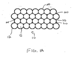
- FIG. 1A is an illustration of a cross-sectional view of a composite material.
- This composite material includes a bed of conductive particles electrochemically sintered together with a compositionally modulated electrodeposited material.
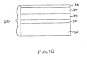
- FIG. 1B is an illustration of an enlarged cross-sectional view of the compositionally modulated electrodeposited material of FIG. 1A .
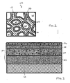
- FIG. 2 is another illustration of a cross-sectional view of a composite material in accordance with another embodiment of the present disclosure.
- This composite material includes a consolidated porous substrate with a compositionally modulated electrodeposited material filling at least a portion of an open, accessible void structure of the porous substrate.
- FIG. 3 is an illustration of a cross-sectional view of the compositionally modulated electrodeposited material of FIG. 2 along one of the voids.
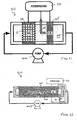
- FIG. 4 is an illustration of an electroplating cell including a working electrode attached to a porous substrate.
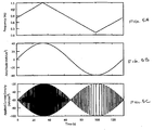
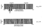
- FIGS. 5A, 5B, 5C , 5D, and 5E are graphs showing electrodeposition conditions and resulting composition maps for the deposition conditions.
- FIG. 5A is a plot of applied frequency to a working electrode in an electrochemical cell versus time.
- FIG. 5B is a plot of applied amplitude to a working electrode in an electrochemical cell versus time.
- FIG. 5C is a plot of applied current density to a working electrode in an electrochemical cell versus time.
- FIG. 5D is an envisioned resulting deposit composition map corresponding to the applied current density given in FIG. 5C (i.e., one frequency modulation cycle of deposition).
- FIG. 5E is an envisioned composition map corresponding to application of ten frequency modulation cycles of deposition.
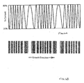
- FIG. 6A is a graph showing a waveform of iron content in a nickel-iron compositionally modulated electrodeposited coating and FIG. 6B is the corresponding composition map.
- FIGS. 7A-7C are illustrations of cross-sectional views of various embodiments of composite materials in accordance with the present disclosure.
- FIG. 7A is an illustration of a composite including an electrochemically infused particle bed having a particle distribution that gradually increases from the exterior surfaces of the composite into the center of the composite.
- FIGS. 7B and 7C are other illustrations of a composite including an electrochemically infused particle bed.
- the particles In FIG. 7B , the particles have a repeating size distribution.
- the particles have a graded distribution.
- FIGS. 8A and 8B are illustrations of two separate embodiments of a compositionally modulated material disposed within the void structure between four particles.
- FIG. 9 is an illustration of a cross-sectional view of an embodiment of a composite material including a nanostructured capping layer deposited on an exterior surface of a porous substrate.
- FIG. 10 is an illustration of a cross-sectional view of an embodiment of a consolidated, conductive porous substrate with a tailored filling of a compositionally modulated electrodeposit coating disposed within its accessible void structure.
- Deposition conditions for this embodiment have been tailored to not only vary a thickness of the coating throughout the depth of the consolidated conductive porous substrate, but also to cap or seal the composite with a dense compositionally modulated layer that closes off accessibility to the interior void structure.
- FIG. 11 is an illustration of a flow cell for electrodepositing a compositionally modulated material into a void structure of an electrically conductive porous substrate.
- FIG. 12 is an illustration of a flow cell for electrodepositing a compositionally modulated material into a void structure of an electrically non-conductive porous substrate.
- FIGS. 13A, 13B, and 13C illustrate deposition conditions and a resulting compositionally modulating electrodeposit for Example 6.
- FIG. 13A is a graph of the frequency and duty cycle modulation waveform for producing the applied current density waveform shown in FIG. 13B.
- FIG. 13C is a cross-sectional view of the compositionally modulating material that is produced under the applied current shown in FIG. 13B .
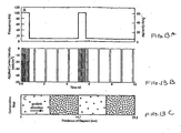
- FIG. 1A shows an exemplary composite material 10 including a porous substrate 12 that is electrochemically sintered or held together by a compositionally modulated electrodeposited material 20.
- the porous substrate 12 shown in FIG. 1A consists of a bed of conductive particles 15 that are hexagonally, closed packed to form a structure that has at least about 26% by volume of open accessible void space 25 due to the arrangement of the particles 15.
- a compositionally modulated material 20 is deposited within the open void space 25 to electrochemically sinter the particles together to form the composite material 10.
- the compositionally modulated electrodeposited material 20, shown in an enlarged cross-sectional view in FIG. 1B includes at least two constituents.
- compositionally modulated describes a material in which the chemical composition varies throughout at least one spatial coordinate, such as, for example, the material's depth.
- the resulting compositionally modulated electrodeposited material 20 includes alloys having a chemical make-up according to Ni x Fe 1-x , where x is a function of applied current or voltage and mass flow of the bath solution.
- the chemical make-up of a deposited layer can be controlled and varied through its depth (i.e., growth direction).
- the compositionally modulated electrodeposited material 20 shown in FIG. 1B includes several different alloys as illustrated by layers 30, 32, 34, 36, and 38.
- layers 32 and 36 represent nickel-rich (x>0.5) deposits, whereas layers 30, 34, and 38 represent iron-rich (x ⁇ 0.5) deposits. While layers 32 and 36 are both nickel rich deposits, the value for x in each of layers 32 and 36 need not be the same. For example, the x value in layer 32 may be 0.7 whereas the x value in layer 36 may be 0.6. Likewise, the x values in layers 30, 34, and 38 can also vary or remain constant. In addition to the composition of the constituents (e.g., Ni and Fe) varying through the depth of the electrodeposited material 20, a thickness of each of the layers 30 to 38 varies through the depth as well. FIG. 1B , while not to scale, illustrates the change or modulation in thickness through the layers 30, 32, 34, 36, and 38.
- the constituents e.g., Ni and Fe
- FIG. 2 illustrates another embodiment of the composite material 10.
- the porous substrate 12 is a consolidated porous body. That is, the porous substrate 12 in this embodiment is a unitary piece that includes a plurality of voids 25 that define an accessible, interior void structure. Examples of consolidated porous bodies include, foams, fabrics, meshes, and partially sintered compacts.
- the compositionally modulated material 20 is electrodeposited throughout the accessible, interior void structure to form a coating along the walls of the substrate 12 defining the voids 25.
- the compositionally modulated material 20 disposed within the plurality of voids 25 includes multiple alloys illustrated as distinct layers 30, 32, 34, and 36. As described above the compositionally modulated material 20 is varied in both constituent concentration (i.e., to form the different alloy layers making up the material 20) and in thickness of the layers.
- the nickel-rich layers 32 and 36 further include a concentration of particles disposed therein, thereby forming particle-reinforced composite layers. As shown in FIG. 3 , layers 32 and 36 need not include the same concentration of particles, thereby allowing the compositionally modulated material 20 to be further tailored to provide optimal material properties.
- the concentration of particles per layer can be controlled through modulating the flow rate of the bath during electrodeposition.
- the particles can have any shape, such as spherical particles, pyramidal particles, rectangular particles, or irregularly shaped particles.
- the particles can be of any length scale, such as for example, millimeter sized (e.g., 1 to 5 millimeter), micron-sized (e.g., 100 microns to 0.1 microns), nanometer sized (e.g., 100 nm to 1 nm).
- 85% or more (e.g., 87%, 89%, 90%, 93%, 95%, 96%, 97%, 98%, 99%, 100%) of the nanosized particles have an average grain size within a range of 10 nm to 100 nm. In certain embodiments, 85% or more of the nanosized particles have an average grain size within a range of 20 nm to 50 nm, 30 nm to 50 nm, 10 nm to 30 nm, or 1 to 10 nm. Examples of some suitable particles include carbide particles, alumina particles, glass particles, polymer particles, silicon carbide fibers, and clay platelets.
- an electrodeposition cell 50 in one embodiment, includes a bath 55 of two or more of metal salts, a cathode (i.e., working electrode) 60, an anode (i.e., a counter electrode) 65, and a potentiostat 70, which electrically connects and controls the applied current between the working and counter electrodes, 60 and 65, respectively.
- the cell 50 can also include a reference electrode 75 to aid the potentiostat 70 in accurately controlling the applied current by providing a reference base line current measurement.
- the porous substrate 12 is positioned in contact with the working electrode 60.
- the porous substrate is formed of a conductive material and functions as an extension of the working electrode 60.
- the resulting product of the oxidation/reduction reaction deposits within the accessible interior void structure 25.
- the porous substrate 12 is formed of a nonconductive material and thus, electrodeposition occurs at a junction between the working electrode 60 and the porous substrate 12.
- one of the advantages of the methods and resulting composite materials described in this disclosure is a wide range of choices of materials available for deposition into the interior void structure 25 of the porous substrate 12.
- salts of any transition metal can be used to form the bath 55.
- some preferred materials include salts of the following metals: nickel, iron, copper, cobalt, gold, silver, and platinum.
- electrodeposition techniques have an additional advantage of easily modifiable processing conditions. For example, a ratio of the metal salts and other electrodepositable components, such as, for example, alumina particles, can be controlled by their concentration within the bath.
- a bath that has a Ni:Fe ratio of 1:1, 2:1, 3:1, 5:1, 10:1 or 20:1 by increasing or decreasing the concentration of a Fe salt within the bath in comparison to the Ni salt prior to deposition.
- Such ratios can thus be achieved for any of the electrodepositable components.
- a bath with Ni, Fe and Cu salts could yield ratios of Ni:Fe of 1:2 and a Ni:Cu of 1:3, making the overall ratio ofNi:Fe:Cu 1:2:3.
- a bath with Ni salt and alumina particles could yield a ratio of Ni:Al 2 O 3 of 2:1, 2:1, 1:2, 3:1 or 1:3 by increasing or decreasing the concentration of particles within the bath.
- FIGS. 5A, 5B, and 5C illustrate applied conditions to the electrochemical cell 50 for depositing the compositionally modulated material 20.
- FIG. 5D illustrates a resulting composition map for the applied conditions shown in FIGS. 5A, 5B, and 5C.
- FIG. 5C shows the current density over a period of 130 seconds applied to the working electrode 60. The applied current drives the oxidation/reduction reaction at the electrode to deposits a material product having the torm A x B 1-x , where A is a first bath constituent and B is a second bath constituent.
- a composition cycle 80 defines the deposition of a pair of layers.
- the first layer of the composition cycles is a A-rich and the second layer is B-rich.
- Each composition cycle has a wavelength.
- the compositionally modulated electrodeposited material 20 includes multiple composition cycles 20 (e.g., 5 composition cycles, 10 composition cycles, 20 composition cycles, 50 composition cycles, 100 composition cycles, 1,000 composition cycles, 10,000 composition cycles, 100,000 composition cycles or more).
- the applied current density as shown in FIG. 5C is determined from an applied variation in frequency of the current per time ( FIG. 5A ) in combination with an applied variation in amplitude of the current per time ( FIG. 5B ).
- an applied frequency modulation shown here as a triangle wave, effects the wavelength of the composition cycles.
- the wavelength of the composition cycles decreases as the frequency increases. While FIG. 5A illustrates this effect with an applied triangle wave, any waveform (i.e., a value that changes with time) may be applied to control or modulate the frequency and thus control or modulate the thickness/wavelengths of the deposited material 20.
- Examples of other waveforms that may be applied to tailor the changing thickness/wavelength of each of the deposited layers/composition cycles include sine waves, square waves, sawtooth waves, and any combination of these waveforms.
- the composition of the deposit i.e., x value
- FIG. 5B illustrates a sine wave modulation of the applied amplitude of the current applied to the working electrode. By changing the amplitude over time, the value of x varies over time such that not all of the Ni-rich layers have the same composition (nor do all the Fe-rich layers have the same composition). Referring to FIGS.
- the value of x is modulated within each of the layers, such that the compositionally modulated electrodeposited material 20 is graded to minimize or mask composition discontinuities.
- the compositionally modulated electrodeposited material 20 can be tailored to include layers that provide a wide range of material properties and enhancements.
- compositionally modulated electrodeposited material 20 is deposited to include one or more regions, which provide the composite material 10 with the supermodulus effect.
- the compositionally modulated electrodeposited material 20 disposed within the void structure 25 of the porous substrate 12 includes one or more regions in which all of the composition cycles include wavelengths less than 200 nm, and preferably less than about 80 nm. In one embodiment, the wavelengths are less than about 70 nm.
- the hardness of the composite material 10 is enhanced by including varying concentrations of particles (e.g., Al 2 O 3 , SiC, Si 3 N 4 ) within an electrodeposited metal. For example, by increasing the concentration of Al 2 O 3 particles dispersed within layers of an electrodeposited Ni metal, an increase in Vicker's Hardness from 240 VHN to 440 VHN is achievable.
- the compositionally modulated electrodeposited material 20 can include regions in which the composition cycles 80 include wavelengths less than 200 nm (and thus which may exhibit the supermodulus effect) and also include regions in which some portion (e.g., at least or about: 1%, 2%, 5%, 7%, 10%, 20%, 30%, 40%, 50%, 60%, 70%, 80%, 90%, 92% 95%, 97%, 99% and 100%) of the composition cycles 80 include wavelengths greater than 200 nm.
- the portion(s) of the composition cycles 80 that include wavelengths greater than 200 nm could also be represented in ranges.
- the composition cycles 80 of one or more regions could include a number of wavelengths greater than 200 nm in a range of from 1-2%, 2-5%, 1-5%, 5-7%, 5-10%, 1-10%, 10-20%, 20-30%, 30-40%, 40-50%, 50-60%, 60-70%, 70-80%, 80-90%, 90-92%, 90-95%, 95-97%, 95-99%, 95-100%, 90-100%, 80-100%, etc., with the balance of the composition cycles being less than 200 nm in that region.
- the compositionally modulated electrodeposited material 20 in some embodiments, can include one or more regions in which all of the composition cycles 80 have a wavelength of about 200 nm or less, one or more regions in which all of the composition cycles have a wavelength greater than 200 nm, and/or one or more regions in which a portion of the composition cycles 80 have a wavelength of about 200 nm or less and a portion have a wavelength greater than 200 nm. Within each of those portions, the wavelengths also can be adjusted to be of a desired size or range of sizes.
- the region(s) having composition cycles of a wavelength of about 200 nm or less can themselves have wavelengths that vary from region to region or even within a region.
- one region may have composition cycles having a wavelength of from 80-150 nm and another region in which the wavelengths are less than 80 nm.
- one region could have both composition cycles of from 80-150 nm and less than 80 nm.
- the compositionally modulated material 20 is tailored to minimize (e.g., prevent) delamination of its layers during use. For example, it is believed that when a projectile impacts a conventional laminated material, the resulting stress waves may cause delamination or debonding due to the presence of discontinuities.
- the compositionally modulated electrodeposited material 20 described herein can include a substantially continuous modulation of both its composition (i.e., x value) and wavelength such that discontinuities are minimized or eliminated, thereby preventing delamination.
- the porous substrate material 12 in addition to compositionally modulating the electrodeposited material 20 to form the composite 10, can also be made of a material that is modulated through its depth.
- the porous substrate 12 is formed of particles 15 that gradually increase in size from an exterior 100 of the compact to an interior 110 of the composite 10.
- the particles in such embodiments can range from, e.g., 5 nm on the exterior 100 to 50 microns in the interior 110, 5 nm on the exterior 100 to 10 microns in the interior 110, 5 nm on the exterior to 1 micron in the interior 110, 10 nm on the exterior 100 to 10 microns in the interior 110, or from 10 nm on the exterior 100 to 1 micron in the interior.
- the differently sized particles 15 contribute to the material properties of the composite 10. For example, smaller particles have a greater surface area energy per unit volume than larger particles of the same material.
- the porous substrate can be tailored to provide additional advantageous material properties to different regions of the composite 10. Referring to FIGS. 7B and 7C , the porous substrate 12 can have other particle arrangements to provide different material properties to the composite 10. For example, in FIG. 7B the particles have a repetitive size distribution and in FIG. 7C the particles have a graded distribution.
- FIGS. 8A and 8B show an enlarged cross-sectional view of the compositionally modulated electrodeposited material 20 disposed between four adjacent particles 15 of a porous substrate 12.
- the particles 15 forming the porous substrate 12 are non-conductive particles (e.g., alumina particles, glass particles).
- electrodeposition occurs between two electrodes disposed on either end of the porous substrate 12 and the compositionally modulated electrodeposited material 20 is deposited in a bottom-up fashion.
- the compositionally modulated electrodeposited material fills the entire void structure 25 between the four particles.
- the particles 15 are electrically conductive.
- electrodeposition can occur within the conductive porous material to produce layers that are initiated at a particle/void interface 120 and grow inwards to fill at least a portion of the interior void structure 25.
- the compositionally modulated material 20 can also be deposited on the exterior surfaces 100 of the porous substrate 12.
- an additional or capping layer 150 can be deposited onto the substrate to seal off the interior porous structure 25 as shown in FIG. 9 .
- the filling of the accessible interior void structure 25 is tailored such that the thickness of the compositionally modulating electrodeposited material 20 varies throughout the composite 10.
- FIG. 10 illustrates a composite material 10 formed of a porous conductive foam 12 and a Ni x Fe 1-x compositionally modulated material 20.
- the thickness of the compositionally modulated material 20 continuously increases (i.e., thickens) from the interior portion 110 of the porous substrate 12 to the exterior 100. To create this thickening, the current density during deposition is continuously increased.
- a dense layer of the compositionally modulated material referred to as the capping layer 150 is further applied to the exterior 100 of the substrate 12 to close off the accessible pore structure 25.
- Methods of forming the composite 10 using electrodeposition can include the following steps: (1) forming a bath including at least two electrodepositable components, (2) connecting the porous preform 12 to the working electrode 60, (3) inserting the porous preform 12, the working electrode 60, and the counter electrode 65 into the bath 55, and (4) applying a voltage or current to the working electrode 60 to drive electrodeposition.
- the voltage or current applied to the working electrode 60 varies over time so that the compositionally modulated material is electrodeposited into the voids 25 of the porous substrate 12.
- the voltage or current is applied to the electrode 60 with a time varying frequency that oscillates in accordance with a triangle wave.
- the voltage or current is applied to the electrode with a time varying frequency that oscillates in accordance with a sine wave, a square wave, a saw-tooth wave, or any other waveform, such as a combination of the foregoing waveforms.
- the voltage or current can be applied for one waveform cycle as shown in FIG. 5A , or preferably for two or more cycles (e.g., three cycles, five cycles, 10 cycles, 20 cycles).
- FIG. 5E shows the envisioned composition map for a 10 cycle deposit.
- the pH of the bath is controlled during electrodeposition. For example, prior to deposition a pH set point (e.g., a pH of 1, 2, 3, 4, 5, 6, 7, 8, 9, 10, 11, 12, 13 or 14) or range (e.g., a pH of 1-2, 2-3, 3-4, 5-6, 6-7, 7-8, 8-9, 9-10, 10-11, 11-12, 12-13, or 13-14) is determined. During electrodeposition, the pH of the bath is monitored and if a difference from the set point is determined, pH altering chemicals, such as, for example, HCl or NaOH, are added to the bath to return the bath to its pH set point.
- pH altering chemicals such as, for example, HCl or NaOH
- the concentration of the electrodepositable components in the bath can also be monitored and controlled.
- concentration sensors can be positioned within the cell 50 to monitor the concentrations of the metal salts as well as any depositable particles within the bath.
- the concentrations of the depositable components e.g., metal salts, particles
- the concentrations of the depositable components can become depleted or at least decreased from a predetermined optimal level within the bath.
- the timeliness of the deposition of the compositionally modulated material 20 can be effected.
- by monitoring and replenishing the concentrations of the depositable components electrodeposition can be optimized.
- flow rate of the bath can be modulated or varied. As described above, both the applied current or voltage and the mass flow rate of the depositable components effects the x-value of the electrodeposit (e.g., Ni x Fe 1-x ). Thus, in some embodiments, the flow rate of the bath containing the depositable components is varied in addition to the applied voltage or current to produce the modulation in the value of x. In other embodiments, the applied voltage or current remains constant and the flow rate is varied to produce the modulation in the value of x.
- the flow rate of the bath can be increased or decreased by providing agitation, such as, for example, a magnetically-controlled mixer or by adding a pump to the cell 50.
- FIGS. 11 and 12 illustrate embodiments of an electrochemical cell 50 that includes a pump 200.
- these cells 50 are referred to as flow cells because they force a bath solution through a porous substrate.
- the flow cell includes a porous working electrode 60, which is also the porous electrically-conductive substrate 12, and a porous counter electrode 65.
- the working electrode 60, the counter electrode 65 and the reference electrode 75 are in communication and are controlled by the potentiostat 70.
- the bath fluid 55 including the depositable components is forced through the porous working electrode 60 (and thus the porous substrate 12) and the counter electrode 65 at a flow rate adjustable at the pump 200.
- the flow rate of the pump 200 can be controlled in accordance with a triangle wave, square wave, sine wave, a saw tooth wave, or any other waveform, such that the flow rate can be modulated to produce the compositionally modulated material 20.
- FIG. 12 illustrates another embodiment of a flow cell 50 for use with non-conductive porous substrates 12.
- the working electrode 60 and the counter electrode 65 are disposed within a wall of the cell 50 and the bath fluid 55 is forced through the porous non-conductive substrate 12. Electrodeposition occurs in a bottom-up fashion, that is the deposition of material 20 proceeds from the working electrode 6U to the counter electrode 65 substantially filling the void structure 25 along the way.
- the porous substrate 12 forming the matrix of the composite material 10 can be formed of a light-weigh ceramic material or can include a relatively large amount (e.g., 40% by volume, 50% by volume, 60% by volume) of accessible interior void space 25.
- the compositionally modulated material 20 electrodeposited into the accessible, interior void space 25 can be tailored to provide strength at least in part through nanolaminate regions and ductility at least in part through micron or submicron sized laminated regions.
- a composite including a Ni foam porous substrate and an electrodeposited compositionally modulated NiFe alloy was formed in a laboratory using the following procedure.
- a bath was prepared using 0.2M Ni(H 2 NSO 3 ) 2 ⁇ 4H 2 O, 0.04 FeCl 2 ⁇ 4H 2 O, 0.40M H 3 BO 3 , 1.5 g/L sodium saccharin, 0.2 g/L sodium dodecyl sulfate, 1.0 g/L ascorbic acid, and HCl to attain a pH of 3.00 ⁇ 0.01.
- a 5 cm long, 1 cm wide, and 0.16 cm thick piece ofNi foam (commonly referred to a Incofoam) having a pore size of 450 microns was wrapped in vinyl electrical tape about the width and thickness of the foam such that 4 cm of length remained uncovered on one end and 0.5 cm of length remained uncovered on the other end.
- the vinyl covered portions of the foam were compressed by hand.
- the 4 cm of exposed Ni foam was dipped into a solution including 0.1M HCl to condition the substrate.
- a potentiostat (available from Gamry Instruments, Warminster, PA, part number PCl/300) was made using an alligator clip connected to the 0.5 cm-long exposed end of the nickel foam.
- a 0.5 cm by 2 cm by 3 cm piece of 40 ppi reticulated vitreous carbon was connected to the counter electrode end of the potentiostat using an alligator clip and a saturated calomel electrode (i.e., a SCE) was connected to the reference electrode terminal.
- a saturated calomel electrode i.e., a SCE
- the Ni foam, the reticulated vitreous carbon, and the SCE were immersed into the bath. Care was taken to ensure that the vinyl wrap about the Ni foam was positioned in the bath-air interface.
- the time-varying current was designed to have the following waveform characteristics: (1) the current density varied in accordance with a square-wave having a maximum deposition current of -100 mA/cm 2 and a minimum deposition current of -10 mA/cm 2 ; (2) a duty cycle of 0.17 with the "off" part of the cycle corresponding to a current density setting of -10 mA/cm 2 ; and (3) a frequency modulation according to a triangle waveform having a peak of 5.5 Hz, a minimum of 0.02 Hz, and a modulation rate of 0.01 Hz.
- the time-varying current was applied to the working electrode until a total of 10 frequency cycles had passed (i.e., 1,000 seconds of time, 10 microns of growth).
- a composite including a porous substrate formed of a piece of carbon fabric and an electrodeposited compositionally modulated NiFe alloy was formed in a laboratory using the following procedure.
- a bath was prepared using 0.2M Ni(H 2 NSO 3 ) 2 ⁇ 4H 2 O, 0.04 FeCl 2 ⁇ 4H 2 O, 0.40M H 3 BO 3 , 1.5 g/L sodium saccharin, 0.2 g/L sodium dodecyl sulfate, 1.0 g/L ascorbic acid, and NaOH to attain a pH of 3.00 ⁇ 0.01.
- a piece of wet laid carbon fabric (commercially available from MarkTek, Inc. of Chesterfield, MO, part number C10001010T) was attached to the working electrode terminal of the potentiostat.
- a 0.5 cm by 2 cm by 3 cm piece of 40 ppi reticulated vitreous carbon was connected to the counter electrode end of the potentiostat using an alligator clip and a saturated calomel electrode (i.e., a SCE) was connected to the reference electrode terminal.
- a saturated calomel electrode i.e., a SCE
- the wet laid carbon fabric, the reticulated vitreous carbon, and the SCE were immersed into the bath.
- the time-varying voltage was designed to have the following waveform characteristics: (1) the voltage versus the SCE varied in accordance with a square-wave having a maximum of -4V and a minimum of -1.5V; (2) a duty cycle of 0.17 with the "off" part of the cycle corresponding to a voltage of -1.5V; and (3) a frequency modulation according to a triangle waveform having a peak of 5.5 Hz, a minimum of 0.02 Hz, and a modulation rate of 0.01Hz.
- the time-varying voltage was applied to the working electrode until a total of 10 frequency cycles had passed (i.e., 1,000 seconds of time).
- a composite including a metallized polyurethane foam substrate and an electrodeposited compositionally modulated NiFe alloy may be formed in a laboratory using the following procedure.
- a bath is prepared using 0.4M Ni(H 2 NSO 3 ) 2 ⁇ 4H 2 O, 0.04 FeCl 2 ⁇ 4H 2 O, 0.40M H 3 BO 3 , 1.5 g/L sodium saccharin, 0.2 g/L sodium dodecyl sulfate, 1.0 g/L ascorbic acid, and HCl to attain a pH of 3.00 ⁇ 0.01.
- a 1 cm long, 1 cm wide, and 0.25 cm thick piece of metallized, reticulated polyurethane foam having a pore size of about 450 microns and a specific surface area of approximately 1200 cm 2 /cm 3 is inserted and secured as the working electrode in a flow cell similar to the flow cell shown in FIG. 11 .
- a piece of 100 ppi reticulated vitreous carbon foam is inserted and secured as the counter electrode in the flow cell. Electrical contact is made between the working electrode and the potentiostat as well as between the counter electrode and the potentiostat.
- a reference electrode is not used in this example.
- a time-varying current is applied to the working electrode to drive the electrodeposition reaction.
- the time-varying current is designed to have the following waveform characteristics: (1) an amperage varying in accordance with a square-wave with a maximum absolute amperage of -23A and a minimum absolute amperage of -5A; (2) a duty cycle of about 11% with the "off' part of the cycle corresponding to an amperage of -5A; and (3) a frequency modulation according to a triangle waveform having a peak of 1.9 Hz, a minimum of 0.019 Hz, and a modulation rate of 0.0075 Hz.
- a control waveform for the flow rate has the following characteristics: (1) a square-wave having a maximum flow rate of 500 mL/min and a minimum flow rate of 2 mL/min is set to control the boundary conditions of flow; (2) a duty cycle of about 11% with the "off" part corresponding to a flow rate of 500 mL/min; and (3) a frequency modulation according to a triangle waveform having a peak of 1.9 Hz, a minimum of 0.019 Hz, and a modulation rate of 0.0075 Hz.
- the current and flow waveforms should be in-phase with the 500 mL/min flow rate setting corresponding to the -5A and the 2 mL/min coinciding with - 23A. Both the time-varying current and the time-varying flow being applied to the working electrode until a total of 10 frequency cycles had passed (i.e., 1,333 seconds of time).
- a composite including a polyurethane, non-conductive foam substrate and an electrodeposited compositionally modulated NiFe alloy may be formed in a laboratory using the following procedure.
- a bath is prepared using 0.4M Ni(H 2 NSO 3 ) 2 ⁇ 4H 2 O, 0.04 FeCl 2 ⁇ 4H 2 O, 0.40M H 3 BO 3 , 1.5 g/L sodium saccharin, 0.2 g/L sodium dodecyl sulfate, 1.0 g/L ascorbic acid, and HCl to attain a pH of 3.00 ⁇ 0.01.
- a sheet of stainless steel, serving as the working electrode, is introduced into a flow cell, such as the flow cell shown in FIG. 12 .
- a piece of 100 ppi reticulated polyurethane foam (i.e., the porous non-conductive substrate) is then positioned above and in contact with the working electrode.
- a piece of wet laid carbon fibers or an additional steel sheet is positioned on top of the polyurethane foam to serve as the counter electrode. Electrical contact is made between the working electrode and the potentiostat as well as between the counter electrode and the potentiostat.
- a reference electrode is not used in this example.
- a time-varying current is applied to the working electrode to drive the electrodeposition reaction.
- the time-varying current is designed to have the following waveform characteristics: (1) a current density that varies accordance with a square-wave with a maximum current density of -100 mA/cm 2 and minimum current density of -20 mA/cm 2 ; (2) a duty cycle of about 11 % with the "off" part of the cycle corresponding to a current density of -20 mA/cm 2 ; and (3) a frequency modulation according to a triangle waveform navmg a peak of 1.9 Hz, a minimum of 0.019 Hz, and a modulation rate of 0.0075 Hz.
- a control waveform for the flow rate has the following characteristics: (1) a square-wave having a maximum flow rate of 636 mL/min and a minimum flow rate of 2.5 mL/min is set to control the boundary conditions of flow; (2) a duty cycle of about 11 % with the "off" part corresponding to a flow rate of 636 mL/min; and (3) a frequency modulation according to a triangle waveform having a peak of 1.9 Hz, a minimum of 0.019 Hz, and a modulation rate of 0.0075 Hz.
- the current and flow waveforms should be in-phase with the 636 mL/min flow rate setting corresponding to the -20A and the 2.5 mL/min coinciding with -100A. Both the time-varying current and the time-varying flow being applied to the working electrode until the voltage of the cell reaches 1 mV (indicating that the deposited growth front is approaching the counter electrode).
- a composite including a bed of conductive metal hollow spheres electrochemically sintered together with an electrodeposited compositionally modulated NiFe alloy may be formed in a laboratory using the following procedure.
- a bath is prepared using 0.4M Ni(H 2 NSO 3 ) 2 ⁇ 4H 2 O, 0.04 FeCl 2 ⁇ 4H 2 O, 0.40M H 3 BO 3 , 1.5 g/L sodium saccharin, 0.2 g/L sodium dodecyl sulfate, 1.0 g/L ascorbic acid, and HCl to attain a pH of 3.00 ⁇ 0.01.
- a bed of conductive, copper, hollow spheres having a mean diameter of 500 microns and positioned between two porous nonconductive screens is inserted and secured as the working electrode in a flow cell similar to the flow cell shown in FIG. 11 .
- a piece of 100 ppi reticulated vitreous carbon foam is inserted and secured as the counter electrode in the flow cell. Electrical contact is made between the working electrode and the potentiostat as well as between the counter electrode and the potentiostat.
- a reference electrode is used to monitor the potential of the working electrode.
- a time-varying current is applied to the working electrode to drive the electrodeposition reaction.
- the time-varying current is designed to have the following waveform characteristics: (1) a current density varying in accordance with a square-wave with a maximum current density of -100 mA/cm 2 and a minimum current density of -20 mA/cm 2 ; (2) a duty cycle of about 11% with the "off" part of the cycle corresponding to a current density of -20 mA/cm 2 ; and (3) a frequency modulation according to a triangle waveform having a peak of 1.9 Hz, a minimum of 0.019 Hz, and a modulation rate of 0.0075 Hz.
- a control waveform for the flow rate has the following characteristics: (1) a square-wave having a maximum flow rate of 636 mL/min and a minimum flow rate of 2.5 mL/min is set to control the boundary conditions of flow; (2) a duty cycle of about 11 % with the "off" part corresponding to a flow rate of 636 mL/min; and (3) a frequency modulation according to a triangle waveform having a peak of 1.9 Hz, a minimum of 0.019 Hz, and a modulation rate of 0.0075 Hz.
- the current and flow waveforms should be in-phase with the 636 mL/min flow rate setting corresponding to the -20 mA/cm 2 and the 2.5 mL/min coinciding with -100 mA/cm 2 . Both the time-varying current and the time-varying flow being applied to the working electrode until a total of 40 frequency cycles had passed.
- a composite including a bed of non-conductive, polymer spheres electrochemically sintered together with an electrodeposited compositionally modulated NiFe alloy may be formed in a laboratory using the following procedure.
- a bath is prepared using 0.4M Ni(H 2 NSO 3 ) 2 ⁇ 4H 2 O, 0.04 FeCl 2 ⁇ 4H 2 O, 0.40M H 3 BO 3 , 1.5 g/L sodium saccharin, 0.2 g/L sodium dodecyl sulfate, 1.0 g/L ascorbic acid, and HCl to attain a pH of 3.00 ⁇ 0.01.
- a sheet of stainless steel, serving as the working electrode, is introduced into a flow cell, such as the flow cell shown in FIG. 12 .
- a bed of polymer spheres having a mean diameter of about 500 microns are packed on top of the working electrode.
- a piece of wet laid carbon fabric or an additional steel sheet is positioned on top of the polymer spheres to serve as the counter electrode.
- a piece of nonconductive, polymer foam can be used to secure the ends of the particle bed not constrained by the electrodes. Electrical contact is made between the working electrode and the potentiostat as well as between the counter electrode and the potentiostat.
- a reference electrode is not used in this example.
- a time-varying current is applied to the working electrode to drive the electrodeposition reaction.
- the time-varying current is designed to have the following waveform characteristics: (1) a current density that varies accordance with a square-wave with a maximum current density of -100 mA/cm 2 and minimum current density of -20 mA/cm 2 ; (2) a duty cycle of about 11 % with the "off" part of the cycle corresponding to a current density of -20 mA/cm 2 ; and (3) a frequency modulation according to a triangle waveform having a peak of 1.9 Hz, a minimum of 0.019 Hz, and a modulation rate of 0.0075 Hz.
- a control waveform for the flow rate has the following characteristics: (1) a square-wave having a maximum flow rate of 636 mL/min and a minimum flow rate of 2.5 mL/min is set to control the boundary conditions of flow; (2) a duty cycle of about 11% with the "off" part corresponding to a flow rate of 636 mL/min; and (3) a frequency modulation according to a triangle waveform having a peak of 1.9 Hz, a minimum of 0.019 Hz, and a modulation rate of 0.0075 Hz.
- the current and flow waveforms should be in-phase with the 636 mL/min flow rate setting corresponding to the -20A and the 2.5 mL/min coinciding with -100A. Both the time-varying current and the time-varying flow being applied to the working electrode until the voltage of the cell reaches 1 mV (indicating that the deposited growth front is approaching the counter electrode).
- a composite including a metallized, polyurethane foam substrate and an compositionally modulated nickel matrix/alumina particle-reinforced material may be formed in a laboratory using the following procedure.
- a bath is prepared using 3.00 g/L NiSO 4 ⁇ 6H 2 O, 60g/L NiCl 2 ⁇ 6H 2 O, 40 g/L H 3 BO 3 , and 80 g/L of 5 micron sized ⁇ -alumina powder.
- a metallized, reticulated polyurethane foam cylinder having a pore diameter of about 450 microns, a thickness of 0.25 cm, a diameter of 1 cm, and a specific surface area of approximately 1200 cm 2 /cm 3 is inserted and secured as the working electrode in a flow cell similar to the flow cell shown in FIG. 11 .
- a piece of 100 ppi reticulated vitreous carbon foam is inserted and secured as the counter electrode in the flow cell. Electrical contact is made between the working electrode and the potentiostat as well as between the counter electrode and the potentiostat.
- a reference electrode is used to monitor the potential of the working electrode.
- a time-varying current is applied to the working electrode to drive the electrodeposition reaction.
- the time-varying current is designed to have the following waveform characteristics: (1) a current density varying in accordance with a square-wave with a maximum current density of -50 mA/cm 2 and a minimum current density of 0 mA/cm 2 with a mean of -25 mA/cm 2 and an amplitude of 25 mA/m 2 ; (2) a frequency modulation according to a square wave form with a mean of 55 Hz, an amplitude of 45 Hz and a modulation frequency of 2 Hz, with a duty cycle of 14% as illustrated in FIG.
- a composite for use as a lightweight auto body panel can be manufactured using the following procedure. First, a flexible sheet of nickel foam or a metallized, open cell polymer foam is stamped into a desired auto body panel shape using a light-duty press to create a preform. After obtained the desired shape, the stamped foam is connected to a negative terminal on a power supply. A piece of reticulated vitreous carbon foam of a size similar to the stamped foam is then connected to a positive terminal on the power supply.
- the stamped foam and the reticulated vitreous carbon foam are immersed in a 10:1 Ni to Fe bath formed from 0.4M Ni(H 2 NSO 3 ) 2 ⁇ 4H 2 O, 0.04 FeCl 2 ⁇ 4H 2 O, 0.40M H 3 BO 3 , 1.5 g/L sodium saccharin, 0.2 g/L sodium dodecyl sulfate, 1.0 g/L ascorbic acid, and HCl to attain a pH of 3.00 ⁇ 0.01.
- a compositionally modulated Ni x Fe 1-x coating is deposited over the entire surface of the stamped foam until 10 to 20% of the interior void space of the stamped foam is filled.
- the compositionally modulated Ni x Fe 1-x coating includes alternating regions of nanolaminates and microlaminates to provide areas of high hardness and high ductility.
- the current density is increased and deposition is focused on the external surfaces of the stamped panel to close or seal off the interior void structure.
- a 100 micron coating having both high hardness and toughness properties is deposited on the exterior surface of the stamped foam to complete the body panel.
- a composite for use as a lightweight body armor can be manufactured using the following procedure. First, a planar sheet of woven carbon fiber is cut into a desired body panel shape. After obtained the desired shape, the cut sheet of carbon fiber is connected to a negative terminal on a power supply. A piece of reticulated vitreous carbon foam of a size similar to the cut sheet of carbon fiber is then connected to a positive terminal on the power supply.
- the carbon fiber and the reticulated vitreous carbon foam are immersed in a 10:1 Ni to Fe bath formed from 0.4M Ni(H 2 NSO 3 ) 2 ⁇ 4H 2 O, 0.04 FeCl 2 ⁇ 4H 2 O, 0.40M H 3 BO 3 , 1.5 g/L sodium saccharin, 0.2 g/L sodium dodecyl sulfate, 1.0 g/L ascorbic acid, and HCl to attain a pH of 3.00 ⁇ 0.01.
- a compositionally modulated Ni x Fe 1-x coating is deposited over the entire surface of the sheet of carbon fiber until 10 to 20% of the interior void space of is filled.
- the compositionally modulated Ni x Fe 1-x coating includes alternating regions of nanolaminates and microlaminates to provide areas of high hardness and high ductility.
- a piece of reticulated metallized elastomeric foam cut to the same shape as the carbon fiber is attached to the 10 to 20% plated carbon fiber workpiece such that their dominant faces are in intimate electrical contact.
- the workpiece including both the plated carbon fiber sheet and the reticulated metallized elastomeric foam i.e., a graded porous substrate
- the workpiece including both the plated carbon fiber sheet and the reticulated metallized elastomeric foam i.e., a graded porous substrate
- electrodeposition of the compositionally modulated Ni x Fe 1-x continues until 10 to 20% of void space of the reticulated metallized elastomeric foam is filled.
- the current density is increased and deposition is focused on the external surface to close or seal off the interior void structure.
- a 100 micron coating having both high hardness and toughness properties is deposited on the exterior surface of the workpiece to complete the armor body panel.
- a composite for use as a lightweight golf club shaft can be manufactured using the following procedure. First, a stainless steel mandrel is inserted into the center of a woven carbon fiber sleeve sized to fit snugly around the mandrel. The stainless steel mandrel is then connected to a negative terminal of a power supply. A piece of reticulated vitreous carbon foam of a size similar to the stainless steel mandrel is then connected to a positive terminal on the power supply.
- the stainless steel mandrel with woven carbon fiber sleeve and the reticulated vitreous carbon foam are immersed in a 10:1 Ni to Fe bath formed from 0.4M Ni(H 2 NSO 3 ) ⁇ 4H 2 O, 0.04 FeCl 2 ⁇ 4H 2 O, 0.40M H 3 BO 3 , 1.5 g/L sodium saccharin, 0.2 g/L sodium dodecyl sulfate, 1.0 g/L ascorbic acid, and HCl to attain a pH of 3.00 ⁇ 0.01.
- a compositionally modulated Ni x Fe 1-x coating is deposited over the entire surface of the woven carbon fiber sleeve until 10 to 20% of the interior void space of the sleeve is filled.
- the compositionally modulated Ni x Fe 1-x coating includes alternating regions of nanolaminates and micro laminates to provide areas of high hardness and high ductility.
- the current density is increased and deposition is focused on the external surfaces of the sleeve to close or seal off the interior void structure.
- a 100 micron coating having both high hardness and toughness properties is deposited on the exterior surface of the sleeve to complete the golf shaft.
Description
- This application claims the benefit of U.S. Provisional Application Serial Number (U.S.S.N.)
60/707,548 U.S.S.N. 60/707,548 - The disclosure relates generally to composite materials and methods for making them. Among the embodiments described herein are such materials and methods of making such materials, including methods of making electrodeposited compositionally modulated materials. Embodiments of the materials disclosed herein exhibit exceptional structural to weight characteristics.
- In general, today's advanced material applications are subjected to environments and stresses, which benefit from unusual combinations of material properties that cannot be met by metal alloys, ceramic compacts, or polymeric materials alone. For example, in ballistic applications, a material is sought which is lightweight and thus fuel efficient, while at the same time provides great impact absorption properties to prevent injury or mechanical failure to an underlying structure designed to be hit by shrapnel or an exploding device. In aircraft or seacraft applications, materials that are strong, light-weight and at the same time corrosion resistant are also sought. To achieve these and other unusual combinations of material properties, composite materials (i.e., a multiphase material that exhibits a significant proportion of properties of its two or more constituent phases) are employed.
- There are many types of composite materials. For example, particle-reinforced composite materials, fiber-reinforced composite materials, and structural composite materials or layered composite materials are generally well-known. Each type of composite material can include two or more phases wherein one phase makes up the majority of the material and is known as the matrix material and the second phase (an potentially additional phases) make(s) up a lesser extent of the composite and can be dispersed within the matrix material or layered within the matrix material to form a sandwich. The presence of the second and additional phases affects the material properties of the composite material. That is, the material properties of the composite material are dependent upon the material properties of the first phase and the second phase (and additional phases) as well as the amounts of the included phase forming the composite. Thus, the material properties of a composite can be tailored for a specific application by the selection of specific concentrations of the phases, as well as potentially, the sizes, shapes, distribution, and orientations of the included phases.
- In general, a structural composite includes two or more layers of material, wherein one or more of the layers may be formed of a composite material in and of itself (e.g., a fiber-reinforced layer or particle-reinforced layer). Each layer of a structural composite provides a different function or provides a specific material property to the structural composite. For example, in ballistic applications one layer can provide toughness to blunt or plastically deform any sharp projectile, a second layer can provide impact resistance so as to absorb kinetic energy of a ballistic that hits the composite, and a third layer can provide strength so as to maintain structural integrity of the composite even after the composite material has been hit by shrapnel or a projectile. Typically, material transitions between these layers are discontinuous. That is, there is an abrupt change in material properties across an interface formed by two of the layers. It is well known that discontinuities often lead to failures in a composite material. For example, interlaminar failure can occur as a projectile's stress wave travels through a composite plate, impacting each of the interfaces between the layers.
- It is also well known that nanolaminate layers may provide enhanced material properties not achievable by their constituent materials on other length scales. For example, certain bimetallic multilayer systems exhibit an anomalous jump in elastic modulus at a specific nanoscale layer thickness, a phenomenon known as the supermodulus effect. In general, to deposit nanoscale multilayers, systems such as DC magnetron sputtering or other deposition techniques that deposit material on top of a substantially flat surface have been utilized.
Electrodeposition methods and microstructures produced thereby are e.g. disclosed inUS 2004/031691 A1 ,US 2004/178076 A1 ,US 2004/027715 A1 ,US 2004/154925 A1 ,US-B1-6 409 907 ,US-A-2 642 654 , andUS-A-5 268 235 . - The following terms are used throughout this disclosure. "Compositionally Modulated Material" defines a material whose chemical composition can be represented by a periodic function of one or more space coordinates, such as, tor example, a growth direction of the material.
"Composition Cycle" defines the deposition of one cycle of the compositionally modulated material (i.e., the deposition corresponding to one cycle of the periodic function).
"Electrodeposition" defines a process in which electricity drives formation of a deposit on an electrode at least partially submerged in a bath including a component, which forms a solid phase upon either oxidation or reduction.
"Electrodeposited Components" defines constituents of a material deposited using electrodeposition. Electrodeposited components include metal ions forming a metal salt, as well as particles which are deposited in a metal matrix formed by electrodeposition. "Nanolaminate" defines a material that includes a plurality of adjacent layers that each have a thickness of less than about 100 nanometers.
"Wavelength" defines a length equal to the thickness of a composition cycle "Waveform" defines a time-varying signal. - The disclosure herein provides numerous embodiments relating to composite materials and methods for making them. A few of these embodiments are briefly summarized.
- In general, embodiments herein provide composite materials and methods for making them. The composite material includes a compositionally modulated nanolaminate coating electrically deposited into an open, accessible void structure of a porous substrate. As a result of including a nanolaminate within the void structure, the composites can include a greater amount of nanolaminate material per unit volume than can be achieved by depositing a nanolaminate material solely on a two-dimensional surface. In addition, the nanolaminate material as well as other material electrodeposited to form the composites are compositionally modulated in a manner so that discontinuities between layers are minimized or potentially even eliminated.
- In one aspect, embodiments described in the present disclosure are also directed to composite materials that include a substrate material defining an accessible interior void structure, and an electrodeposited compositionally modulated material at least partially disposed within the accessible void structure. The electrodeposited compositionally modulated material includes at least one portion of a plurality of composition cycles having wavelengths between about 200 nanometers and 1 nanometer. In certain embodiments, the at least one portion includes a plurality of composition cycles having wavelengths between about 100 nanometers and 1 nanometer. In other embodiments, the at least one portion includes a plurality of composition cycles having wavelengths between about 75 nanometers and 10 nanometers. In other embodiments, the at least one portion includes a plurality of composition cycles having wavelengths between about 60 nanometers and 25 nanometers.
- Such embodiments can include one or more of the following features. The composite materials may include wavelengths within the at least one portion that are substantially equivalent. That is, a thickness of each of the layers within the at least one portion can all be described as having a substantially similar or equivalent wavelength. In other embodiments, regions within the electrodeposited compositionally modulated material have a composition that varies continuously, such that discontinuities are masked or substantially or completely eliminated. The composite materials can have enhanced or increased structural properties including an enhanced strength or elastic modulus through the supermodulus effect. In addition to having regions wherein at least one portion of a plurality of composition cycles have wavelengths between 200 nanometers and 1 nanometer, the composite materials can also include one or more regions wherein the composition cycles are greater than 200 nanometers. That is, the composite material can include an electrodeposited material that includes at least one portion wherein the thickness of the deposited layers is 100 nanometers, or less and one or more regions wherein the thickness of the deposited material is greater than 100 nanometers. In some embodiments, the electrodeposited compositionally modulated material includes at least one of nickel, iron, copper, cobalt, gold, silver, platinum and combinations thereof. In certain embodiments, the electrodeposited compositionally modulated material includes a metal matrix material and a plurality of particles disposed within the metal matrix material. The particles can be nanosized particles (e.g., particles having a mean grain size of 200 nm, 100 nm, 75 nm, 50 nm, 30 nm, 20 nm, 15 nm, 10 nm, 5 nm, 4 nm 3 nm, 2 nm, or 1 nm) and in some embodiments, 85% or more (e.g., 87%, 89%, 90%, 93%, 95%, 96%, 97%, 98%, 99%, 100%) of the nanosized particles have an average grain size within a range of 10 nm to 100 nm. In certain embodiments, 85% or more of the nanosized particles have an average grain size within a range of 20 nm to 50 nm, 30 nm to 50 nm, 10 nm to 30 nm, or 1 to 10 nm. In some embodiments, the particles are formed of carbide particles, alumina particles, glass particles, and polymer particles. The electrodeposited compositionally modulated material, in some embodiments, fills at least 10% of the accessible interior void structure. In other embodiments, the compositionally modulated material fills at least 20%, 30%, 40%, 50%, 60%, 70%, 80%, or 90% of the accessible interior void structure. In other embodiments, the compositionally modulated material fills 100% of the accessible interior. The substrate material comprises a conductive, consolidated material, such as a foam or a fabric.
- In another aspect, embodiments of this disclosure are directed to a composite material that includes a material defining an accessible interior void structure, and an electrodeposited compositionally modulated material at least partially disposed within the accessible void structure. The electrodeposited compositionally modulated material includes a first portion and a second portion having a Vicker's hardness value at least: 10% greater, (e.g. 20%, 30%, 40%, 50%, 60%, 70%, 80%, 90%, 100%, 150%, 200%, 500% or more) than the first portion.
- Embodiments of this aspect of the disclosure can include one or more of the following features. In some embodiments, the electrodeposited compositionally modulated material includes at least one of nickel, iron, copper, cobalt, gold, silver, platinum and combination thereof. In certain embodiments, the first portion of the electrodeposited compositionally modulated material includes a metal matrix material with a first concentration of particles and the second portion includes the metal matrix with a second concentration of particles, wherein the second concentration of particles is greater than the first concentration. The particles disposed in the metal matrix can be nanosized particles (e.g., particles having a mean grain size of 200 nm, 100 mm, 75 nm, 50 nm, 30 nm, 20 nm, 15 nm, 10 nm, 5 nm, 4 nm 3 nm, 2 nm, or 1 nm) and in some embodiments, 85% or more (e.g., 87%, 89%, 90%, 93%, 95%, 96%, 97%, 98%, 99%, 100%) of the nanosized particles have an average grain size within a range of 10 nm to 100 nm. In certain embodiments, 85% or more of the nanosized particles have an average grain size within a range of 20 nm to 50 nm, 30 nm to 50 nm, 10 nm to 30 nm, or 1 to 10 nm. In some embodiments, the particles are formed of carbide particles, alumina particles, glass particles, and polymer particles. The electrodeposited compositionally modulated material, in some embodiments, fills at least 10% of the accessible interior void structure. In other embodiments, the compositionally modulated material fills at least: 20%, 30%, 40%, 50%, 60%, 70%, 80%, or 90%. In other embodiments, the compositionally modulated material fills substantially (i.e., all or nearly all) 100% of the accessible interior void structure. The substrate material comprises a conductive, consolidated material, such as a foam or a fabric.
- In another aspect, embodiments of the disclosure are directed to methods for forming a composite. The methods include providing a preform having an accessible interior void structure, and electrodepositing a nanolaminate coating into the accessible interior void structure to form the composite.
- In another aspect, embodiments described herein are directed to methods of forming a composite using electrodeposition. The methods includes providing a bath including at least two electrodepositable components; connecting a porous preform including an accessible interior void structure to a first electrode; inserting the porous preform into the bath; inserting a second electrode into the bath; applying voltage or current to the first electrode with a time varying frequency. The time varying frequency as applied oscillates at least for two cycles (e.g., 2, 3, 4, 5, 10, 20, 30, 50, 100 or more) to deposit a compositionally modulated material within the accessible interior void structure of the porous preform.
- In a further aspect, embodiments described herein are directed to methods of forming a composite using electrodeposition. The methods include: (1) flowing a fluid including at least two electrodepositable components through a porous preform having an accessible void structure at a first flow rate, the porous preform being in physical contact with a first electrode; (2) applying a voltage or current between the first electrode and a second electrode to deposit a material at least partially disposed within the void structure, the material including the at least two electrodepositable components; and (3) modulating the flow rate at a time dependent frequency wherein the time dependent frequency oscillates for at least two cycles (e.g., 2, 3, 4, 5, 10, 20, 50, 100 or more) to compositionally modulate the material.
- Embodiments of the above methods can also include one or more of the following optional features. One or more steps of controlling pH of the bath, and/or monitoring and/or adjusting the concentration of the at least two electrodepositable components can be included in the methods described above. For example, in one embodiment, the pH of the bath can be monitored and adjusted during application of the voltage or current to the first electrode. Similarly, the concentration of one or more of the at least two electrodepositable components in the bath can be monitored to detect a difference from a predetermined concentration level tor forming the compositionally modulated material. Upon detection of a difference from the predetermined level for any of the electrodepositable components, the concentration of that component can be adjusted to eliminate or decrease the detected difference. In some embodiments of the methods, the time varying frequency oscillates according to one of a triangle wave, a sine wave, a square wave, a saw tooth wave, or any combination of the foregoing waveforms. In certain embodiments, the flow rate of the bath and/or an applied voltage or current are modulated at a time varying frequency. The bath can include any transition metal, such as, for example, nickel, iron, copper, gold, silver, platinum, and alloys of these elements. In addition, the bath may include particles, such as, for example, alumina particles, silicon carbide particle, silicon nitride particles, or glass particles, that will become disposed within an electrodeposited metal matrix. The electrodeposited compositionally modulated material, in some embodiments, fills at least 10% of the accessible interior void structure. In other embodiments, the compositionally modulated material fills at least: 20%, 30%, 40%, 50%, 60%, 70%, 80%, or 90%. In other embodiments, the compositionally modulated material fills substantially 100% of the accessible interior void structure. In certain embodiments, the compositionally modulated material has a thickness that continuously increases through a portion (e.g., through the depth) of the composite. In some embodiments, the methods can include a step of depositing a compositionally modulated layer on an exterior surface of the composite. The substrate material comprises a consolidated material, such as, a foam or a fabric. The substrate material is conductive. In certain embodiments, the substrate material can be a foam having layers consisting of different porosities.
- In another aspect, embodiments of the disclosure include a method for forming a component, such as, for example, a panel for a vehicle, a frame for a sporting good, or a body panel or plate for a suit of armor. The method includes stamping a porous preform having an accessible interior void structure into a predetermined shape to form an object and electrodepositing a nanolaminate coating to fill at least a portion of the accessible interior void structure of the object to form the component. The nanolaminate coating may be formed using any electrodeposition method, including those methods disclosed herein. In some embodiments, electrodepositing the nanolaminate coating includes applying a voltage or current with a time varying frequency to an electrode submerged in a fluid containing electrodepositable components. In certain embodiments, electrodepositing the nanolaminate coating includes modulating a flow rate of a fluid including electrodepositable components through the accessible interior voids structure at a time dependent frequency.
- In general, the composite material and methods of forming the composite material described above can include one or more of the following advantages. In certain embodiments, composite materials herein described are light in weight but also structurally strong and sound, such that the composite materials can be used in ballistic applications (e.g., body armor panels or tank panels), in automotive, watercraft or aircraft protection applications (e.g., car door panels, racing shells and boat, plane and helicopter body parts) and in sporting equipment applications (e.g., golf club shafts and tennis racket frames). The composite materials may be used in combination with other types of ballistic or structural applications, known now or developed after this disclosure. Due to the open, accessible void structure of the porous substrate prior to deposition of the electrodeposited compositionally modulated material, the composite can include a greater amount per unit volume of material of the electrodeposited material than conventional composites, which include deposits solely along a two-dimensional flat surface. As a result, the composite material in accordance with the features described above can be tailored for applications where it is advantageous for the material properties of the electrodeposited compositionally modulated material to dominate or to provide a greater impact on the overall material properties of the composite material. The compositionally modulated material can be easily deposited using electrodeposition techniques. The electrodeposition techniques described in this application can be used to control and modulate the composition of the deposited material within the void structure. Moreover, the electrodeposition techniques are easily scalable to commercial manufacturing techniques and do not involve relatively expensive equipment, such as, for example, dc magnetron sputtering apparatus, or involve processing under extreme environments, such as toxic gases and vacuum atmospheric conditions. Thus, methods described herein can provide a relatively low cost, efficient means of producing a light-weight, structurally advanced composite material.
- In the drawings, like reference characters generally refer to the same parts throughout the different views. Also, the drawings are not necessarily to scale, emphasis instead being placed upon illustrating the principles of the disclosure.
-
FIG. 1A is an illustration of a cross-sectional view of a composite material. This composite material includes a bed of conductive particles electrochemically sintered together with a compositionally modulated electrodeposited material. -
FIG. 1B is an illustration of an enlarged cross-sectional view of the compositionally modulated electrodeposited material ofFIG. 1A . -
FIG. 2 is another illustration of a cross-sectional view of a composite material in accordance with another embodiment of the present disclosure. This composite material includes a consolidated porous substrate with a compositionally modulated electrodeposited material filling at least a portion of an open, accessible void structure of the porous substrate. -
FIG. 3 is an illustration of a cross-sectional view of the compositionally modulated electrodeposited material ofFIG. 2 along one of the voids. -
FIG. 4 is an illustration of an electroplating cell including a working electrode attached to a porous substrate. -
FIGS. 5A, 5B, 5C ,5D, and 5E are graphs showing electrodeposition conditions and resulting composition maps for the deposition conditions.FIG. 5A is a plot of applied frequency to a working electrode in an electrochemical cell versus time.FIG. 5B is a plot of applied amplitude to a working electrode in an electrochemical cell versus time.FIG. 5C is a plot of applied current density to a working electrode in an electrochemical cell versus time.FIG. 5D is an envisioned resulting deposit composition map corresponding to the applied current density given inFIG. 5C (i.e., one frequency modulation cycle of deposition).FIG. 5E is an envisioned composition map corresponding to application of ten frequency modulation cycles of deposition. -
FIG. 6A is a graph showing a waveform of iron content in a nickel-iron compositionally modulated electrodeposited coating andFIG. 6B is the corresponding composition map. -
FIGS. 7A-7C are illustrations of cross-sectional views of various embodiments of composite materials in accordance with the present disclosure.FIG. 7A is an illustration of a composite including an electrochemically infused particle bed having a particle distribution that gradually increases from the exterior surfaces of the composite into the center of the composite.FIGS. 7B and 7C are other illustrations of a composite including an electrochemically infused particle bed. InFIG. 7B , the particles have a repeating size distribution. InFIG. 7C the particles have a graded distribution. -
FIGS. 8A and 8B are illustrations of two separate embodiments of a compositionally modulated material disposed within the void structure between four particles. -
FIG. 9 is an illustration of a cross-sectional view of an embodiment of a composite material including a nanostructured capping layer deposited on an exterior surface of a porous substrate. -
FIG. 10 is an illustration of a cross-sectional view of an embodiment of a consolidated, conductive porous substrate with a tailored filling of a compositionally modulated electrodeposit coating disposed within its accessible void structure. Deposition conditions for this embodiment have been tailored to not only vary a thickness of the coating throughout the depth of the consolidated conductive porous substrate, but also to cap or seal the composite with a dense compositionally modulated layer that closes off accessibility to the interior void structure. -
FIG. 11 is an illustration of a flow cell for electrodepositing a compositionally modulated material into a void structure of an electrically conductive porous substrate. -
FIG. 12 is an illustration of a flow cell for electrodepositing a compositionally modulated material into a void structure of an electrically non-conductive porous substrate. -
FIGS. 13A, 13B, and 13C illustrate deposition conditions and a resulting compositionally modulating electrodeposit for Example 6.FIG. 13A is a graph of the frequency and duty cycle modulation waveform for producing the applied current density waveform shown inFIG. 13B. FIG. 13C is a cross-sectional view of the compositionally modulating material that is produced under the applied current shown inFIG. 13B . - Referring now to the figures,
FIG. 1A shows an exemplarycomposite material 10 including aporous substrate 12 that is electrochemically sintered or held together by a compositionally modulatedelectrodeposited material 20. Theporous substrate 12 shown inFIG. 1A consists of a bed ofconductive particles 15 that are hexagonally, closed packed to form a structure that has at least about 26% by volume of open accessiblevoid space 25 due to the arrangement of theparticles 15. When positioned within an electrochemical cell under deposition conditions, a compositionally modulatedmaterial 20 is deposited within theopen void space 25 to electrochemically sinter the particles together to form thecomposite material 10. The compositionally modulatedelectrodeposited material 20, shown in an enlarged cross-sectional view inFIG. 1B , includes at least two constituents. The two or more constituents are electrodeposited in a manner such that an amount of the two or more constituents is varied to form different alloy layers within thematerial 20. The term "compositionally modulated" describes a material in which the chemical composition varies throughout at least one spatial coordinate, such as, for example, the material's depth. For example, in an electrochemical bath including a nickel-containing solution and an iron-containing solution, the resulting compositionally modulatedelectrodeposited material 20 includes alloys having a chemical make-up according to NixFe1-x, where x is a function of applied current or voltage and mass flow of the bath solution. Thus, by controlling or modulating at least one of the mass flow of the bath solution or the applied current or voltage to electrodes, the chemical make-up of a deposited layer can be controlled and varied through its depth (i.e., growth direction). As a result, the compositionally modulatedelectrodeposited material 20 shown inFIG. 1B includes several different alloys as illustrated bylayers - Referring to
FIG. 1B , layers 32 and 36 represent nickel-rich (x>0.5) deposits, whereaslayers layers layers layer 32 may be 0.7 whereas the x value inlayer 36 may be 0.6. Likewise, the x values inlayers electrodeposited material 20, a thickness of each of thelayers 30 to 38 varies through the depth as well.FIG. 1B , while not to scale, illustrates the change or modulation in thickness through thelayers -
FIG. 2 illustrates another embodiment of thecomposite material 10. In this embodiment, theporous substrate 12 is a consolidated porous body. That is, theporous substrate 12 in this embodiment is a unitary piece that includes a plurality ofvoids 25 that define an accessible, interior void structure. Examples of consolidated porous bodies include, foams, fabrics, meshes, and partially sintered compacts. The compositionally modulatedmaterial 20 is electrodeposited throughout the accessible, interior void structure to form a coating along the walls of thesubstrate 12 defining thevoids 25. - Referring to
FIG. 3 , the compositionally modulatedmaterial 20 disposed within the plurality of voids 25 (as shown inFIG. 2 ) includes multiple alloys illustrated asdistinct layers material 20 is varied in both constituent concentration (i.e., to form the different alloy layers making up the material 20) and in thickness of the layers. In the embodiment shown inFIG. 3 , the nickel-rich layers FIG. 3 , layers 32 and 36 need not include the same concentration of particles, thereby allowing the compositionally modulatedmaterial 20 to be further tailored to provide optimal material properties. While not wishing to be bound by any particular theory, it is believed that increasing the concentration of the particles in a layer increases the hardness of that particular layer. The concentration of particles per layer can be controlled through modulating the flow rate of the bath during electrodeposition. The particles can have any shape, such as spherical particles, pyramidal particles, rectangular particles, or irregularly shaped particles. In addition, the particles can be of any length scale, such as for example, millimeter sized (e.g., 1 to 5 millimeter), micron-sized (e.g., 100 microns to 0.1 microns), nanometer sized (e.g., 100 nm to 1 nm). In some embodiments, 85% or more (e.g., 87%, 89%, 90%, 93%, 95%, 96%, 97%, 98%, 99%, 100%) of the nanosized particles have an average grain size within a range of 10 nm to 100 nm. In certain embodiments, 85% or more of the nanosized particles have an average grain size within a range of 20 nm to 50 nm, 30 nm to 50 nm, 10 nm to 30 nm, or 1 to 10 nm. Examples of some suitable particles include carbide particles, alumina particles, glass particles, polymer particles, silicon carbide fibers, and clay platelets. - To form or deposit the compositionally modulated
electrodeposited material 20, theporous substrate 12 is submerged into an electrochemical cell. Referring toFIG. 4 , anelectrodeposition cell 50, in one embodiment, includes abath 55 of two or more of metal salts, a cathode (i.e., working electrode) 60, an anode (i.e., a counter electrode) 65, and apotentiostat 70, which electrically connects and controls the applied current between the working and counter electrodes, 60 and 65, respectively. Thecell 50 can also include areference electrode 75 to aid thepotentiostat 70 in accurately controlling the applied current by providing a reference base line current measurement. In general, when an electrical current is passed through thecell 50, an oxidation/reduction reaction involving the metal ions in thebath 55 occurs and the resulting product is deposited on the workingelectrode 60. As shown inFIG. 4 , theporous substrate 12 is positioned in contact with the workingelectrode 60. For example, in certain embodiments, the porous substrate is formed of a conductive material and functions as an extension of the workingelectrode 60. As a result, the resulting product of the oxidation/reduction reaction deposits within the accessible interiorvoid structure 25. In other embodiments, theporous substrate 12 is formed of a nonconductive material and thus, electrodeposition occurs at a junction between the workingelectrode 60 and theporous substrate 12. - In general, one of the advantages of the methods and resulting composite materials described in this disclosure is a wide range of choices of materials available for deposition into the
interior void structure 25 of theporous substrate 12. For example, salts of any transition metal can be used to form thebath 55. Specifically, some preferred materials include salts of the following metals: nickel, iron, copper, cobalt, gold, silver, and platinum. In addition to the wide range of materials available, electrodeposition techniques have an additional advantage of easily modifiable processing conditions. For example, a ratio of the metal salts and other electrodepositable components, such as, for example, alumina particles, can be controlled by their concentration within the bath. Thus, it is possible to provide a bath that has a Ni:Fe ratio of 1:1, 2:1, 3:1, 5:1, 10:1 or 20:1 by increasing or decreasing the concentration of a Fe salt within the bath in comparison to the Ni salt prior to deposition. Such ratios can thus be achieved for any of the electrodepositable components. Where more than two electrodepositable components are provided, such ratios can be achieved as between.any two of the components such that the overall ratios for all components will be that which is desired. For example, a bath with Ni, Fe and Cu salts could yield ratios of Ni:Fe of 1:2 and a Ni:Cu of 1:3, making the overall ratio ofNi:Fe:Cu 1:2:3. In addition, a bath with Ni salt and alumina particles could yield a ratio of Ni:Al2O3 of 2:1, 2:1, 1:2, 3:1 or 1:3 by increasing or decreasing the concentration of particles within the bath. -
FIGS. 5A, 5B, and 5C illustrate applied conditions to theelectrochemical cell 50 for depositing the compositionally modulatedmaterial 20.FIG. 5D illustrates a resulting composition map for the applied conditions shown inFIGS. 5A, 5B, and 5C. FIG. 5C shows the current density over a period of 130 seconds applied to the workingelectrode 60. The applied current drives the oxidation/reduction reaction at the electrode to deposits a material product having the torm AxB1-x, where A is a first bath constituent and B is a second bath constituent. - Another way of defining the modulation of the compositions of the deposited alloys (AxB1-x, where x varies) is with respect to a composition cycle. A
composition cycle 80 defines the deposition of a pair of layers. The first layer of the composition cycles is a A-rich and the second layer is B-rich. Each composition cycle has a wavelength. A value assigned to the wavelength is equal to the thickness of the two layers forming thecomposition cycle 80. That is, the wavelength has a value that is equal to two times the thickness of one of the two layers forming the composition cycle (e.g., λ=10 nm, when thickness ofNi-rich layer within the composition cycle is equal to 5 nm). By including one or more composition cycles the deposited material is compositionally modulating. In a preferred embodiment, the compositionally modulatedelectrodeposited material 20 includes multiple composition cycles 20 (e.g., 5 composition cycles, 10 composition cycles, 20 composition cycles, 50 composition cycles, 100 composition cycles, 1,000 composition cycles, 10,000 composition cycles, 100,000 composition cycles or more). - The applied current density as shown in
FIG. 5C is determined from an applied variation in frequency of the current per time (FIG. 5A ) in combination with an applied variation in amplitude of the current per time (FIG. 5B ). Referring toFIG. 5A , an applied frequency modulation, shown here as a triangle wave, effects the wavelength of the composition cycles. As shown by comparingFIGS. 5A and5D , the wavelength of the composition cycles decreases as the frequency increases. WhileFIG. 5A illustrates this effect with an applied triangle wave, any waveform (i.e., a value that changes with time) may be applied to control or modulate the frequency and thus control or modulate the thickness/wavelengths of the depositedmaterial 20. Examples of other waveforms that may be applied to tailor the changing thickness/wavelength of each of the deposited layers/composition cycles include sine waves, square waves, sawtooth waves, and any combination of these waveforms. The composition of the deposit (i.e., x value) can also be further modulated by varying the amplitude.FIG. 5B illustrates a sine wave modulation of the applied amplitude of the current applied to the working electrode. By changing the amplitude over time, the value of x varies over time such that not all of the Ni-rich layers have the same composition (nor do all the Fe-rich layers have the same composition). Referring toFIGS. 6A and 6B , in some embodiments, the value of x is modulated within each of the layers, such that the compositionally modulatedelectrodeposited material 20 is graded to minimize or mask composition discontinuities. As a result of applying one or more of the above deposition conditions, the compositionally modulatedelectrodeposited material 20 can be tailored to include layers that provide a wide range of material properties and enhancements. - One such enhancement is an increase in hardness. Without wishing to be bound to any particular theory, it is believed that regions of nanolaminate material (i.e., regions in which all of the composition cycles have a wavelength less than about 200 nm and preferably less than about 80 nm) exhibit a superior hardness not achievable by the same materials at greater lengths scales. This superior hardness is believed to arise from an increase in the material's elastic modulus coefficient, and is known as the "supermodulus effect." In certain embodiments, the compositionally modulated
electrodeposited material 20 is deposited to include one or more regions, which provide thecomposite material 10 with the supermodulus effect. That is, the compositionally modulatedelectrodeposited material 20 disposed within thevoid structure 25 of theporous substrate 12 includes one or more regions in which all of the composition cycles include wavelengths less than 200 nm, and preferably less than about 80 nm. In one embodiment, the wavelengths are less than about 70 nm. In another embodiment, the hardness of thecomposite material 10 is enhanced by including varying concentrations of particles (e.g., Al2O3, SiC, Si3N4) within an electrodeposited metal. For example, by increasing the concentration of Al2O3 particles dispersed within layers of an electrodeposited Ni metal, an increase in Vicker's Hardness from 240 VHN to 440 VHN is achievable. - In some embodiments, the compositionally modulated
electrodeposited material 20 can include regions in which the composition cycles 80 include wavelengths less than 200 nm (and thus which may exhibit the supermodulus effect) and also include regions in which some portion (e.g., at least or about: 1%, 2%, 5%, 7%, 10%, 20%, 30%, 40%, 50%, 60%, 70%, 80%, 90%, 92% 95%, 97%, 99% and 100%) of the composition cycles 80 include wavelengths greater than 200 nm. The portion(s) of the composition cycles 80 that include wavelengths greater than 200 nm could also be represented in ranges. For example, the composition cycles 80 of one or more regions could include a number of wavelengths greater than 200 nm in a range of from 1-2%, 2-5%, 1-5%, 5-7%, 5-10%, 1-10%, 10-20%, 20-30%, 30-40%, 40-50%, 50-60%, 60-70%, 70-80%, 80-90%, 90-92%, 90-95%, 95-97%, 95-99%, 95-100%, 90-100%, 80-100%, etc., with the balance of the composition cycles being less than 200 nm in that region. Without wishing to be bound by any particular theory, it is believed that, as hardness increases, ductility decreases. As a result, in order to provide a composite material that is enhanced to include regions of increased hardness and regions of increased ductility, the compositionally modulatedelectrodeposited material 20, in some embodiments, can include one or more regions in which all of the composition cycles 80 have a wavelength of about 200 nm or less, one or more regions in which all of the composition cycles have a wavelength greater than 200 nm, and/or one or more regions in which a portion of the composition cycles 80 have a wavelength of about 200 nm or less and a portion have a wavelength greater than 200 nm. Within each of those portions, the wavelengths also can be adjusted to be of a desired size or range of sizes. Thus, for example, the region(s) having composition cycles of a wavelength of about 200 nm or less can themselves have wavelengths that vary from region to region or even within a region. Thus, is some embodiments, one region may have composition cycles having a wavelength of from 80-150 nm and another region in which the wavelengths are less than 80 nm. In other embodiments, one region could have both composition cycles of from 80-150 nm and less than 80 nm. - In certain embodiments, the compositionally modulated
material 20 is tailored to minimize (e.g., prevent) delamination of its layers during use. For example, it is believed that when a projectile impacts a conventional laminated material, the resulting stress waves may cause delamination or debonding due to the presence of discontinuities. However, the compositionally modulatedelectrodeposited material 20 described herein can include a substantially continuous modulation of both its composition (i.e., x value) and wavelength such that discontinuities are minimized or eliminated, thereby preventing delamination. - Referring to
FIGS. 7A-7C , in addition to compositionally modulating theelectrodeposited material 20 to form the composite 10, theporous substrate material 12 can also be made of a material that is modulated through its depth. For example, as shown inFIG. 7A , in one embodiment, theporous substrate 12 is formed ofparticles 15 that gradually increase in size from anexterior 100 of the compact to an interior 110 of the composite 10. The particles in such embodiments can range from, e.g., 5 nm on the exterior 100 to 50 microns in the interior 110, 5 nm on the exterior 100 to 10 microns in the interior 110, 5 nm on the exterior to 1 micron in the interior 110, 10 nm on the exterior 100 to 10 microns in the interior 110, or from 10 nm on the exterior 100 to 1 micron in the interior. The differentlysized particles 15 contribute to the material properties of the composite 10. For example, smaller particles have a greater surface area energy per unit volume than larger particles of the same material. As a result, the porous substrate can be tailored to provide additional advantageous material properties to different regions of the composite 10. Referring toFIGS. 7B and 7C , theporous substrate 12 can have other particle arrangements to provide different material properties to the composite 10. For example, inFIG. 7B the particles have a repetitive size distribution and inFIG. 7C the particles have a graded distribution. -
FIGS. 8A and 8B show an enlarged cross-sectional view of the compositionally modulatedelectrodeposited material 20 disposed between fouradjacent particles 15 of aporous substrate 12. InFIG. 8A , theparticles 15 forming theporous substrate 12 are non-conductive particles (e.g., alumina particles, glass particles). As a result of their non-conductivity, electrodeposition occurs between two electrodes disposed on either end of theporous substrate 12 and the compositionally modulatedelectrodeposited material 20 is deposited in a bottom-up fashion. Thus, the compositionally modulated electrodeposited material fills theentire void structure 25 between the four particles. In the embodiment shown inFIG. 8B , theparticles 15 are electrically conductive. As a result, electrodeposition can occur within the conductive porous material to produce layers that are initiated at a particle/void interface 120 and grow inwards to fill at least a portion of theinterior void structure 25. - In addition to electrodepositing into a porous preform, the compositionally modulated
material 20 can also be deposited on theexterior surfaces 100 of theporous substrate 12. For example, after the accessible interiorvoid structure 25 is at least partially filled in the case of an electrically conductive porous substrate or substantially filled in the case of a non-conductive porous substrate, an additional orcapping layer 150 can be deposited onto the substrate to seal off the interiorporous structure 25 as shown inFIG. 9 . - In certain embodiments, the filling of the accessible interior
void structure 25 is tailored such that the thickness of the compositionally modulatingelectrodeposited material 20 varies throughout the composite 10. For example,FIG. 10 illustrates acomposite material 10 formed of a porousconductive foam 12 and a NixFe1-x compositionally modulatedmaterial 20. The thickness of the compositionally modulatedmaterial 20 continuously increases (i.e., thickens) from theinterior portion 110 of theporous substrate 12 to theexterior 100. To create this thickening, the current density during deposition is continuously increased. In addition to including the compositionally modulatedmaterial 20 disposed throughout thevoid structure 25 of thesubstrate 12, a dense layer of the compositionally modulated material, referred to as thecapping layer 150 is further applied to theexterior 100 of thesubstrate 12 to close off theaccessible pore structure 25. - Methods of forming the composite 10 using electrodeposition can include the following steps: (1) forming a bath including at least two electrodepositable components, (2) connecting the
porous preform 12 to the workingelectrode 60, (3) inserting theporous preform 12, the workingelectrode 60, and thecounter electrode 65 into thebath 55, and (4) applying a voltage or current to the workingelectrode 60 to drive electrodeposition. - In general, in one embodiment, the voltage or current applied to the working
electrode 60 varies over time so that the compositionally modulated material is electrodeposited into thevoids 25 of theporous substrate 12. Thus, in some embodiments, the voltage or current is applied to theelectrode 60 with a time varying frequency that oscillates in accordance with a triangle wave. In other embodiments, the voltage or current is applied to the electrode with a time varying frequency that oscillates in accordance with a sine wave, a square wave, a saw-tooth wave, or any other waveform, such as a combination of the foregoing waveforms. The voltage or current can be applied for one waveform cycle as shown inFIG. 5A , or preferably for two or more cycles (e.g., three cycles, five cycles, 10 cycles, 20 cycles).FIG. 5E shows the envisioned composition map for a 10 cycle deposit. - In addition to controlling the voltage or current, other deposition conditions can also be monitored and varied to tailor the compositionally modulating
material 20. For example, it is believed that the pH of the bath has an effect on upon the quality of the deposited material. Thus, in some embodiments, the pH of the bath is controlled during electrodeposition. For example, prior to deposition a pH set point (e.g., a pH of 1, 2, 3, 4, 5, 6, 7, 8, 9, 10, 11, 12, 13 or 14) or range (e.g., a pH of 1-2, 2-3, 3-4, 5-6, 6-7, 7-8, 8-9, 9-10, 10-11, 11-12, 12-13, or 13-14) is determined. During electrodeposition, the pH of the bath is monitored and if a difference from the set point is determined, pH altering chemicals, such as, for example, HCl or NaOH, are added to the bath to return the bath to its pH set point. - The concentration of the electrodepositable components in the bath can also be monitored and controlled. For example, concentration sensors can be positioned within the
cell 50 to monitor the concentrations of the metal salts as well as any depositable particles within the bath. During electrodeposition of the compositionally modulatedmaterial 20, the concentrations of the depositable components (e.g., metal salts, particles) can become depleted or at least decreased from a predetermined optimal level within the bath. As a result, the timeliness of the deposition of the compositionally modulatedmaterial 20 can be effected. Thus, by monitoring and replenishing the concentrations of the depositable components electrodeposition can be optimized. - In certain embodiments, flow rate of the bath can be modulated or varied. As described above, both the applied current or voltage and the mass flow rate of the depositable components effects the x-value of the electrodeposit (e.g., NixFe1-x). Thus, in some embodiments, the flow rate of the bath containing the depositable components is varied in addition to the applied voltage or current to produce the modulation in the value of x. In other embodiments, the applied voltage or current remains constant and the flow rate is varied to produce the modulation in the value of x. The flow rate of the bath can be increased or decreased by providing agitation, such as, for example, a magnetically-controlled mixer or by adding a pump to the
cell 50. -
FIGS. 11 and 12 illustrate embodiments of anelectrochemical cell 50 that includes apump 200. In general, thesecells 50 are referred to as flow cells because they force a bath solution through a porous substrate. Referring toFIG. 11 , the flow cell includes a porous workingelectrode 60, which is also the porous electrically-conductive substrate 12, and aporous counter electrode 65. The workingelectrode 60, thecounter electrode 65 and thereference electrode 75 are in communication and are controlled by thepotentiostat 70. Thebath fluid 55 including the depositable components is forced through the porous working electrode 60 (and thus the porous substrate 12) and thecounter electrode 65 at a flow rate adjustable at thepump 200. Thus, in certain embodiments, the flow rate of thepump 200 can be controlled in accordance with a triangle wave, square wave, sine wave, a saw tooth wave, or any other waveform, such that the flow rate can be modulated to produce the compositionally modulatedmaterial 20. -
FIG. 12 illustrates another embodiment of aflow cell 50 for use with non-conductiveporous substrates 12. In thiscell 50, the workingelectrode 60 and thecounter electrode 65 are disposed within a wall of thecell 50 and thebath fluid 55 is forced through the porousnon-conductive substrate 12. Electrodeposition occurs in a bottom-up fashion, that is the deposition ofmaterial 20 proceeds from the working electrode 6U to thecounter electrode 65 substantially filling thevoid structure 25 along the way. - The methods and composite materials described herein can be tailored to provide the unusual combination of strength, ductility, and low-density. For example, the
porous substrate 12 forming the matrix of thecomposite material 10 can be formed of a light-weigh ceramic material or can include a relatively large amount (e.g., 40% by volume, 50% by volume, 60% by volume) of accessible interiorvoid space 25. The compositionally modulatedmaterial 20 electrodeposited into the accessible,interior void space 25 can be tailored to provide strength at least in part through nanolaminate regions and ductility at least in part through micron or submicron sized laminated regions. These composite materials can be utilized in automotive applications, ballistic applications, sporting good applications, or any other application that would benefit from this combination of material properties. - The following examples are provided to further illustrate and to facilitate the understanding of the disclosure. These specific examples are intended to be illustrative of the disclosure and are not intended to be limiting.
- A composite including a Ni foam porous substrate and an electrodeposited compositionally modulated NiFe alloy was formed in a laboratory using the following procedure. A bath was prepared using 0.2M Ni(H2NSO3)2·4H2O, 0.04 FeCl2·4H2O, 0.40M H3BO3, 1.5 g/L sodium saccharin, 0.2 g/L sodium dodecyl sulfate, 1.0 g/L ascorbic acid, and HCl to attain a pH of 3.00 ± 0.01. A 5 cm long, 1 cm wide, and 0.16 cm thick piece ofNi foam (commonly referred to a Incofoam) having a pore size of 450 microns was wrapped in vinyl electrical tape about the width and thickness of the foam such that 4 cm of length remained uncovered on one end and 0.5 cm of length remained uncovered on the other end. The vinyl covered portions of the foam were compressed by hand. The 4 cm of exposed Ni foam was dipped into a solution including 0.1M HCl to condition the substrate.
- Electrical connection between the Ni foam and a working electrode terminal of a potentiostat, (available from Gamry Instruments, Warminster, PA, part number PCl/300) was made using an alligator clip connected to the 0.5 cm-long exposed end of the nickel foam. To complete electrical connections between the electrodes and the potentiostat, a 0.5 cm by 2 cm by 3 cm piece of 40 ppi reticulated vitreous carbon was connected to the counter electrode end of the potentiostat using an alligator clip and a saturated calomel electrode (i.e., a SCE) was connected to the reference electrode terminal.
- After confirming electrical communication between the potentiostat and the working electrode, counter electrode, and reference electrode, the Ni foam, the reticulated vitreous carbon, and the SCE were immersed into the bath. Care was taken to ensure that the vinyl wrap about the Ni foam was positioned in the bath-air interface.
- Once positioned within the bath, a time-varying current was applied to the working electrode. The time-varying current was designed to have the following waveform characteristics: (1) the current density varied in accordance with a square-wave having a maximum deposition current of -100 mA/cm2 and a minimum deposition current of -10 mA/cm2; (2) a duty cycle of 0.17 with the "off" part of the cycle corresponding to a current density setting of -10 mA/cm2; and (3) a frequency modulation according to a triangle waveform having a peak of 5.5 Hz, a minimum of 0.02 Hz, and a modulation rate of 0.01 Hz. The time-varying current was applied to the working electrode until a total of 10 frequency cycles had passed (i.e., 1,000 seconds of time, 10 microns of growth).
- A composite including a porous substrate formed of a piece of carbon fabric and an electrodeposited compositionally modulated NiFe alloy was formed in a laboratory using the following procedure. A bath was prepared using 0.2M Ni(H2NSO3)2·4H2O, 0.04 FeCl2·4H2O, 0.40M H3BO3, 1.5 g/L sodium saccharin, 0.2 g/L sodium dodecyl sulfate, 1.0 g/L ascorbic acid, and NaOH to attain a pH of 3.00 ± 0.01. A piece of wet laid carbon fabric (commercially available from MarkTek, Inc. of Chesterfield, MO, part number C10001010T) was attached to the working electrode terminal of the potentiostat. To complete electrical connections between the electrodes and the potentiostat, a 0.5 cm by 2 cm by 3 cm piece of 40 ppi reticulated vitreous carbon was connected to the counter electrode end of the potentiostat using an alligator clip and a saturated calomel electrode (i.e., a SCE) was connected to the reference electrode terminal.
- After confirming electrical communication between the potentiostat and the working electrode, counter electrode, and reference electrode, the wet laid carbon fabric, the reticulated vitreous carbon, and the SCE were immersed into the bath.
- Once positioned within the bath, a time-varying voltage was applied to the working electrode. The time-varying voltage was designed to have the following waveform characteristics: (1) the voltage versus the SCE varied in accordance with a square-wave having a maximum of -4V and a minimum of -1.5V; (2) a duty cycle of 0.17 with the "off" part of the cycle corresponding to a voltage of -1.5V; and (3) a frequency modulation according to a triangle waveform having a peak of 5.5 Hz, a minimum of 0.02 Hz, and a modulation rate of 0.01Hz. The time-varying voltage was applied to the working electrode until a total of 10 frequency cycles had passed (i.e., 1,000 seconds of time).
- A composite including a metallized polyurethane foam substrate and an electrodeposited compositionally modulated NiFe alloy may be formed in a laboratory using the following procedure. A bath is prepared using 0.4M Ni(H2NSO3)2·4H2O, 0.04 FeCl2·4H2O, 0.40M H3BO3, 1.5 g/L sodium saccharin, 0.2 g/L sodium dodecyl sulfate, 1.0 g/L ascorbic acid, and HCl to attain a pH of 3.00 ± 0.01. A 1 cm long, 1 cm wide, and 0.25 cm thick piece of metallized, reticulated polyurethane foam having a pore size of about 450 microns and a specific surface area of approximately 1200 cm2/cm3 is inserted and secured as the working electrode in a flow cell similar to the flow cell shown in
FIG. 11 . A piece of 100 ppi reticulated vitreous carbon foam is inserted and secured as the counter electrode in the flow cell. Electrical contact is made between the working electrode and the potentiostat as well as between the counter electrode and the potentiostat. A reference electrode is not used in this example. - After confirming electrical communication between the potentiostat and the working electrode and the counter electrode, a time-varying current is applied to the working electrode to drive the electrodeposition reaction. The time-varying current is designed to have the following waveform characteristics: (1) an amperage varying in accordance with a square-wave with a maximum absolute amperage of -23A and a minimum absolute amperage of -5A; (2) a duty cycle of about 11% with the "off' part of the cycle corresponding to an amperage of -5A; and (3) a frequency modulation according to a triangle waveform having a peak of 1.9 Hz, a minimum of 0.019 Hz, and a modulation rate of 0.0075 Hz. In addition to applying a time-varying current, a time-varying flow rate is also applied to the flow cell through the pump. A control waveform for the flow rate has the following characteristics: (1) a square-wave having a maximum flow rate of 500 mL/min and a minimum flow rate of 2 mL/min is set to control the boundary conditions of flow; (2) a duty cycle of about 11% with the "off" part corresponding to a flow rate of 500 mL/min; and (3) a frequency modulation according to a triangle waveform having a peak of 1.9 Hz, a minimum of 0.019 Hz, and a modulation rate of 0.0075 Hz. The current and flow waveforms should be in-phase with the 500 mL/min flow rate setting corresponding to the -5A and the 2 mL/min coinciding with - 23A. Both the time-varying current and the time-varying flow being applied to the working electrode until a total of 10 frequency cycles had passed (i.e., 1,333 seconds of time).
- A composite including a polyurethane, non-conductive foam substrate and an electrodeposited compositionally modulated NiFe alloy may be formed in a laboratory using the following procedure. A bath is prepared using 0.4M Ni(H2NSO3)2·4H2O, 0.04 FeCl2·4H2O, 0.40M H3BO3, 1.5 g/L sodium saccharin, 0.2 g/L sodium dodecyl sulfate, 1.0 g/L ascorbic acid, and HCl to attain a pH of 3.00 ± 0.01. A sheet of stainless steel, serving as the working electrode, is introduced into a flow cell, such as the flow cell shown in
FIG. 12 . A piece of 100 ppi reticulated polyurethane foam (i.e., the porous non-conductive substrate) is then positioned above and in contact with the working electrode. To complete the cell, a piece of wet laid carbon fibers or an additional steel sheet is positioned on top of the polyurethane foam to serve as the counter electrode. Electrical contact is made between the working electrode and the potentiostat as well as between the counter electrode and the potentiostat. A reference electrode is not used in this example. - After confirming electrical communication between the potentiostat and the working electrode and the counter electrode, a time-varying current is applied to the working electrode to drive the electrodeposition reaction. The time-varying current is designed to have the following waveform characteristics: (1) a current density that varies accordance with a square-wave with a maximum current density of -100 mA/cm2 and minimum current density of -20 mA/cm2; (2) a duty cycle of about 11 % with the "off" part of the cycle corresponding to a current density of -20 mA/cm2; and (3) a frequency modulation according to a triangle waveform navmg a peak of 1.9 Hz, a minimum of 0.019 Hz, and a modulation rate of 0.0075 Hz. In addition to applying a time-varying current, a time-varying flow rate is also applied to the flow cell through the pump. A control waveform for the flow rate has the following characteristics: (1) a square-wave having a maximum flow rate of 636 mL/min and a minimum flow rate of 2.5 mL/min is set to control the boundary conditions of flow; (2) a duty cycle of about 11 % with the "off" part corresponding to a flow rate of 636 mL/min; and (3) a frequency modulation according to a triangle waveform having a peak of 1.9 Hz, a minimum of 0.019 Hz, and a modulation rate of 0.0075 Hz. The current and flow waveforms should be in-phase with the 636 mL/min flow rate setting corresponding to the -20A and the 2.5 mL/min coinciding with -100A. Both the time-varying current and the time-varying flow being applied to the working electrode until the voltage of the cell reaches 1 mV (indicating that the deposited growth front is approaching the counter electrode).
- A composite including a bed of conductive metal hollow spheres electrochemically sintered together with an electrodeposited compositionally modulated NiFe alloy may be formed in a laboratory using the following procedure. A bath is prepared using 0.4M Ni(H2NSO3)2·4H2O, 0.04 FeCl2·4H2O, 0.40M H3BO3, 1.5 g/L sodium saccharin, 0.2 g/L sodium dodecyl sulfate, 1.0 g/L ascorbic acid, and HCl to attain a pH of 3.00 ± 0.01. A bed of conductive, copper, hollow spheres having a mean diameter of 500 microns and positioned between two porous nonconductive screens is inserted and secured as the working electrode in a flow cell similar to the flow cell shown in
FIG. 11 . A piece of 100 ppi reticulated vitreous carbon foam is inserted and secured as the counter electrode in the flow cell. Electrical contact is made between the working electrode and the potentiostat as well as between the counter electrode and the potentiostat. A reference electrode is used to monitor the potential of the working electrode. - After confirming electrical communication between the potentiostat and the working electrode, the counter electrode, and the reference electrode, a time-varying current is applied to the working electrode to drive the electrodeposition reaction. The time-varying current is designed to have the following waveform characteristics: (1) a current density varying in accordance with a square-wave with a maximum current density of -100 mA/cm2 and a minimum current density of -20 mA/cm2; (2) a duty cycle of about 11% with the "off" part of the cycle corresponding to a current density of -20 mA/cm2; and (3) a frequency modulation according to a triangle waveform having a peak of 1.9 Hz, a minimum of 0.019 Hz, and a modulation rate of 0.0075 Hz. In addition to applying a time-varying current, a time-varying flow rate is also applied to the flow cell through the pump. A control waveform for the flow rate has the following characteristics: (1) a square-wave having a maximum flow rate of 636 mL/min and a minimum flow rate of 2.5 mL/min is set to control the boundary conditions of flow; (2) a duty cycle of about 11 % with the "off" part corresponding to a flow rate of 636 mL/min; and (3) a frequency modulation according to a triangle waveform having a peak of 1.9 Hz, a minimum of 0.019 Hz, and a modulation rate of 0.0075 Hz. The current and flow waveforms should be in-phase with the 636 mL/min flow rate setting corresponding to the -20 mA/cm2 and the 2.5 mL/min coinciding with -100 mA/cm2. Both the time-varying current and the time-varying flow being applied to the working electrode until a total of 40 frequency cycles had passed.
- A composite including a bed of non-conductive, polymer spheres electrochemically sintered together with an electrodeposited compositionally modulated NiFe alloy may be formed in a laboratory using the following procedure. A bath is prepared using 0.4M Ni(H2NSO3)2·4H2O, 0.04 FeCl2·4H2O, 0.40M H3BO3, 1.5 g/L sodium saccharin, 0.2 g/L sodium dodecyl sulfate, 1.0 g/L ascorbic acid, and HCl to attain a pH of 3.00 ± 0.01. A sheet of stainless steel, serving as the working electrode, is introduced into a flow cell, such as the flow cell shown in
FIG. 12 . A bed of polymer spheres having a mean diameter of about 500 microns are packed on top of the working electrode. To complete the cell, a piece of wet laid carbon fabric or an additional steel sheet is positioned on top of the polymer spheres to serve as the counter electrode. A piece of nonconductive, polymer foam can be used to secure the ends of the particle bed not constrained by the electrodes. Electrical contact is made between the working electrode and the potentiostat as well as between the counter electrode and the potentiostat. A reference electrode is not used in this example. - After confirming electrical communication between the potentiostat and the working electrode and the counter electrode, a time-varying current is applied to the working electrode to drive the electrodeposition reaction. The time-varying current is designed to have the following waveform characteristics: (1) a current density that varies accordance with a square-wave with a maximum current density of -100 mA/cm2 and minimum current density of -20 mA/cm2; (2) a duty cycle of about 11 % with the "off" part of the cycle corresponding to a current density of -20 mA/cm2; and (3) a frequency modulation according to a triangle waveform having a peak of 1.9 Hz, a minimum of 0.019 Hz, and a modulation rate of 0.0075 Hz. In addition to applying a time-varying current, a time-varying flow rate is also applied to the flow cell through the pump. A control waveform for the flow rate has the following characteristics: (1) a square-wave having a maximum flow rate of 636 mL/min and a minimum flow rate of 2.5 mL/min is set to control the boundary conditions of flow; (2) a duty cycle of about 11% with the "off" part corresponding to a flow rate of 636 mL/min; and (3) a frequency modulation according to a triangle waveform having a peak of 1.9 Hz, a minimum of 0.019 Hz, and a modulation rate of 0.0075 Hz. The current and flow waveforms should be in-phase with the 636 mL/min flow rate setting corresponding to the -20A and the 2.5 mL/min coinciding with -100A. Both the time-varying current and the time-varying flow being applied to the working electrode until the voltage of the cell reaches 1 mV (indicating that the deposited growth front is approaching the counter electrode).
- A composite including a metallized, polyurethane foam substrate and an compositionally modulated nickel matrix/alumina particle-reinforced material may be formed in a laboratory using the following procedure. A bath is prepared using 3.00 g/L NiSO4·6H2O, 60g/L NiCl2·6H2O, 40 g/L H3BO3, and 80 g/L of 5 micron sized α-alumina powder. A metallized, reticulated polyurethane foam cylinder having a pore diameter of about 450 microns, a thickness of 0.25 cm, a diameter of 1 cm, and a specific surface area of approximately 1200 cm2/cm3 is inserted and secured as the working electrode in a flow cell similar to the flow cell shown in
FIG. 11 . A piece of 100 ppi reticulated vitreous carbon foam is inserted and secured as the counter electrode in the flow cell. Electrical contact is made between the working electrode and the potentiostat as well as between the counter electrode and the potentiostat. A reference electrode is used to monitor the potential of the working electrode. - After confirming electrical communication between the potentiostat and the working electrode, the counter electrode, and the reference electrode and setting the pump to a constant flow rate of 50 ML/min, a time-varying current is applied to the working electrode to drive the electrodeposition reaction. The time-varying current is designed to have the following waveform characteristics: (1) a current density varying in accordance with a square-wave with a maximum current density of -50 mA/cm2 and a minimum current density of 0 mA/cm2 with a mean of -25 mA/cm2 and an amplitude of 25 mA/m2; (2) a frequency modulation according to a square wave form with a mean of 55 Hz, an amplitude of 45 Hz and a modulation frequency of 2 Hz, with a duty cycle of 14% as illustrated in
FIG. 13A ; and (3 ) a duty cycle modulation according to a square waveform with a mean of 35%, and an amplitude of 25%, and a modulation frequency of 2% as illustrated inFIG. 13A . The time-varying current (seeFIG. 13B ) being applied to the working electrode until a total of 10,000 frequency modulation cycles have passed (e.g., 5,000 seconds) to form a compositionally modulated electrodeposit that has a Ni matrix and layers of various concentrations of alumina particles as illustrated inFIG. 13C . - A composite for use as a lightweight auto body panel can be manufactured using the following procedure. First, a flexible sheet of nickel foam or a metallized, open cell polymer foam is stamped into a desired auto body panel shape using a light-duty press to create a preform. After obtained the desired shape, the stamped foam is connected to a negative terminal on a power supply. A piece of reticulated vitreous carbon foam of a size similar to the stamped foam is then connected to a positive terminal on the power supply. After confirming electrical communication, the stamped foam and the reticulated vitreous carbon foam are immersed in a 10:1 Ni to Fe bath formed from 0.4M Ni(H2NSO3)2·4H2O, 0.04 FeCl2·4H2O, 0.40M H3BO3, 1.5 g/L sodium saccharin, 0.2 g/L sodium dodecyl sulfate, 1.0 g/L ascorbic acid, and HCl to attain a pH of 3.00 ± 0.01. A compositionally modulated NixFe1-x coating is deposited over the entire surface of the stamped foam until 10 to 20% of the interior void space of the stamped foam is filled. The compositionally modulated NixFe1-x coating includes alternating regions of nanolaminates and microlaminates to provide areas of high hardness and high ductility.
- After filling 10 to 20% of the interior void space, the current density is increased and deposition is focused on the external surfaces of the stamped panel to close or seal off the interior void structure. A 100 micron coating having both high hardness and toughness properties is deposited on the exterior surface of the stamped foam to complete the body panel.
- A composite for use as a lightweight body armor can be manufactured using the following procedure. First, a planar sheet of woven carbon fiber is cut into a desired body panel shape. After obtained the desired shape, the cut sheet of carbon fiber is connected to a negative terminal on a power supply. A piece of reticulated vitreous carbon foam of a size similar to the cut sheet of carbon fiber is then connected to a positive terminal on the power supply. After confirming electrical communication, the carbon fiber and the reticulated vitreous carbon foam are immersed in a 10:1 Ni to Fe bath formed from 0.4M Ni(H2NSO3)2·4H2O, 0.04 FeCl2·4H2O, 0.40M H3BO3, 1.5 g/L sodium saccharin, 0.2 g/L sodium dodecyl sulfate, 1.0 g/L ascorbic acid, and HCl to attain a pH of 3.00 ± 0.01. A compositionally modulated NixFe1-x coating is deposited over the entire surface of the sheet of carbon fiber until 10 to 20% of the interior void space of is filled. The compositionally modulated NixFe1-x coating includes alternating regions of nanolaminates and microlaminates to provide areas of high hardness and high ductility.
- Next a piece of reticulated metallized elastomeric foam cut to the same shape as the carbon fiber is attached to the 10 to 20% plated carbon fiber workpiece such that their dominant faces are in intimate electrical contact. The workpiece including both the plated carbon fiber sheet and the reticulated metallized elastomeric foam (i.e., a graded porous substrate) is immersed in the 10:1 Ni to Fe bath and electrodeposition of the compositionally modulated NixFe1-x continues until 10 to 20% of void space of the reticulated metallized elastomeric foam is filled.
- A piece of conductive, high-hardness reticulated carbon foam such as, for example, CFOAM® (available from Touchstone Research Laboratory, Triadelphia, WV) is cut and electrically joined to the workpiece. The workpiece including the three layers (carbon fiber, reticulated metallized elastomeric foam, and CFOAM®) is immersed in the 10:1 Ni to Fe bath and electrodeposition of the compositionally modulated NixFe1-x continues until 10 to 20% of the void space in the CFOAM® is filled.
- After filling 10 to 20% of the interior void space of the entire workpiece, the current density is increased and deposition is focused on the external surface to close or seal off the interior void structure. A 100 micron coating having both high hardness and toughness properties is deposited on the exterior surface of the workpiece to complete the armor body panel.
- A composite for use as a lightweight golf club shaft can be manufactured using the following procedure. First, a stainless steel mandrel is inserted into the center of a woven carbon fiber sleeve sized to fit snugly around the mandrel. The stainless steel mandrel is then connected to a negative terminal of a power supply. A piece of reticulated vitreous carbon foam of a size similar to the stainless steel mandrel is then connected to a positive terminal on the power supply. After confirming electrical communication, the stainless steel mandrel with woven carbon fiber sleeve and the reticulated vitreous carbon foam are immersed in a 10:1 Ni to Fe bath formed from 0.4M Ni(H2NSO3)·4H2O, 0.04 FeCl2·4H2O, 0.40M H3BO3, 1.5 g/L sodium saccharin, 0.2 g/L sodium dodecyl sulfate, 1.0 g/L ascorbic acid, and HCl to attain a pH of 3.00 ± 0.01. A compositionally modulated NixFe1-x coating is deposited over the entire surface of the woven carbon fiber sleeve until 10 to 20% of the interior void space of the sleeve is filled. The compositionally modulated NixFe1-x coating includes alternating regions of nanolaminates and micro laminates to provide areas of high hardness and high ductility.
- After filling 10 to 20% of the interior void space, the current density is increased and deposition is focused on the external surfaces of the sleeve to close or seal off the interior void structure. A 100 micron coating having both high hardness and toughness properties is deposited on the exterior surface of the sleeve to complete the golf shaft.
Claims (25)
- A composite material comprising:a substrate material defining an accessible interior void structure; wherein the substrate material comprises a conductive, consolidated material selected from the group consisting of a foam and a fabric; andan electrodeposited compositionally modulated material at least partially disposed within the accessible void structure, the electrodeposited compositionally modulated material including at least one portion consisting of a plurality of composition cycles having wavelengths between about 200 nm and 1 nm.
- The composite material of claim 1, wherein the wavelengths within the at least one portion are substantially equivalent.
- The composite material of claim 1, wherein the wavelengths vary continuously within the at least one portion.
- The composite material of claim 1, wherein the electrodeposited compositionally modulated material includes regions of deposition including a wavelength greater than 200 nm.
- The composite material of claim 1, wherein the electrodeposited compositionally modulated material includes at least one of nickel, iron, copper, cobalt, gold, silver, platinum and combinations thereof.
- The composite material of claim 1, wherein the electrodeposited compositionally modulated material includes a metal matrix material and a plurality of particles disposed within the metal matrix material.
- The composite material of claim 6, wherein the plurality of particles include nanosized particles.
- The composite material of claim 6, wherein the plurality of particles are selected from the group consisting of carbide particles, alumina particles, glass particles, and polymer particles.
- A method for forming a composite material according to claim 1, using electrodeposition, the method comprising:flowing a fluid including at least two electrodepositable components through a porous preform having an accessible void structure at a flow rate, the porous preform being in physical contact with a first electrode; wherein the porous preform comprises a conductive, consolidated material selected from the group consisting of a foam and a fabric;applying a voltage or current between the first electrode and a second electrode to deposit a material at least partially disposed within the void structure and including the at least two electrodepositable components; andmodulating the flow rate at a time dependent frequency wherein the time dependent frequency oscillates for at least two cycles to compositionally modulate the material.
- The method of claim 9 further comprising: monitoring concentration of the at least two electrodepositable components to detect a difference from a predetermined concentration level.
- The method of claim 10 further comprising adjusting the concentration of one or more of the at least two electrodepositable components upon the detection of the difference from the predetermined concentration level.
- The method of claim 9, wherein the time dependent frequency oscillates according to a square wave.
- The method of claim 9, wherein the time dependent frequency oscillates according to a triangle wave.
- The method of claim 9, wherein the time dependent frequency oscillates according to a sine wave.
- The method of claim 9, wherein the at least two electrodepositable components are selected from the group consisting of nickel, iron, copper, cobalt, gold, silver, platinum and combinations thereof.
- The method of claim 9, wherein the bath comprises particles disposed within a metal matrix.
- The method of claim 9, wherein the preform comprises a graded element.
- The method of claim 9 further comprising: electrodepositing a compositionally modulated layer on an exterior surface of the composite.
- The method of claim 9 further comprising: controlling pH of the bath while modulating the flow rate.
- A method for forming a component, the method comprising:stamping a porous preform having an accessible interior void structure into a predetermined shape to form an object; wherein the porous preform comprises a conductive, consolidated material selected from the group consisting of a foam and a fabric; andelectrodepositing a nanolaminate coating to fill a portion of the accessible interior void structure of the object to form the component.
- The method of claim 20, wherein the predetermined shape of the object is a panel for a vehicle.
- The method of claim 20, wherein the predetermined shape of the object is a frame for a sporting good.
- The method of claim 20, wherein the predetermined shape of the object is a plate for armor.
- The method of claim 20, wherein electrodepositing the nanolaminate coating comprises applying voltage or current with a time dependent frequency to a fluid containing an electrodepositable components wherein the time dependent frequency oscillates at least for two cycles to deposit a compositionally modulated material within the accessible interior void structure.
- The method of claim 20, wherein electrodepositing the nanolaminate coating comprises modulating a flow rate of a fluid including an electrodepositable components through the accessible interior void structure at a time dependent frequency wherein the time dependent frequency oscillates for at least two cycles.
Priority Applications (1)
| Application Number | Priority Date | Filing Date | Title |
|---|---|---|---|
| EP11001879.3A EP2381015B1 (en) | 2005-08-12 | 2006-08-14 | Compositionally modulated composite materials |
Applications Claiming Priority (2)
| Application Number | Priority Date | Filing Date | Title |
|---|---|---|---|
| US70754805P | 2005-08-12 | 2005-08-12 | |
| PCT/US2006/031455 WO2007021980A2 (en) | 2005-08-12 | 2006-08-14 | Compositionally modulated composite materials and methods for making the same |
Related Child Applications (2)
| Application Number | Title | Priority Date | Filing Date |
|---|---|---|---|
| EP11001879.3A Division EP2381015B1 (en) | 2005-08-12 | 2006-08-14 | Compositionally modulated composite materials |
| EP11001879.3 Division-Into | 2011-03-07 |
Publications (3)
| Publication Number | Publication Date |
|---|---|
| EP1919703A2 EP1919703A2 (en) | 2008-05-14 |
| EP1919703A4 EP1919703A4 (en) | 2008-11-12 |
| EP1919703B1 true EP1919703B1 (en) | 2013-04-24 |
Family
ID=37758224
Family Applications (2)
| Application Number | Title | Priority Date | Filing Date |
|---|---|---|---|
| EP20060801305 Active EP1919703B1 (en) | 2005-08-12 | 2006-08-14 | Compositionally modulated composite materials and methods for making the same |
| EP11001879.3A Active EP2381015B1 (en) | 2005-08-12 | 2006-08-14 | Compositionally modulated composite materials |
Family Applications After (1)
| Application Number | Title | Priority Date | Filing Date |
|---|---|---|---|
| EP11001879.3A Active EP2381015B1 (en) | 2005-08-12 | 2006-08-14 | Compositionally modulated composite materials |
Country Status (6)
| Country | Link |
|---|---|
| US (2) | US9115439B2 (en) |
| EP (2) | EP1919703B1 (en) |
| JP (1) | JP5301993B2 (en) |
| CA (1) | CA2619509C (en) |
| ES (1) | ES2422455T3 (en) |
| WO (1) | WO2007021980A2 (en) |
Families Citing this family (41)
| Publication number | Priority date | Publication date | Assignee | Title |
|---|---|---|---|---|
| US7320832B2 (en) | 2004-12-17 | 2008-01-22 | Integran Technologies Inc. | Fine-grained metallic coatings having the coefficient of thermal expansion matched to the one of the substrate |
| EP1919703B1 (en) | 2005-08-12 | 2013-04-24 | Modumetal, LLC | Compositionally modulated composite materials and methods for making the same |
| WO2008097358A2 (en) * | 2006-09-12 | 2008-08-14 | Jamin Micarelli | Lightweight armor composite, method of making same, and articles containing the same |
| WO2009045593A2 (en) * | 2007-07-06 | 2009-04-09 | Modumetal, Llc | Nanolaminate-reinforced metal composite tank material and design for storage of flammable and combustible fluids |
| US9273932B2 (en) * | 2007-12-06 | 2016-03-01 | Modumetal, Inc. | Method of manufacture of composite armor material |
| US9005420B2 (en) * | 2007-12-20 | 2015-04-14 | Integran Technologies Inc. | Variable property electrodepositing of metallic structures |
| JP5056575B2 (en) * | 2008-05-12 | 2012-10-24 | ソニー株式会社 | Resin composition, electronic device, and method for manufacturing electronic device |
| WO2010005983A2 (en) | 2008-07-07 | 2010-01-14 | Modumetal Llc | Property modulated materials and methods of making the same |
| US20110114496A1 (en) * | 2008-07-15 | 2011-05-19 | Dopp Robert B | Electrochemical Devices, Systems, and Methods |
| US20140099472A1 (en) * | 2008-08-11 | 2014-04-10 | Greenhill Antiballistics Corporation | Composite material |
| CA2696048C (en) | 2008-08-11 | 2016-05-03 | Greenhill Antiballistics Corporation | Composite material |
| EP2440691B1 (en) * | 2009-06-08 | 2019-10-23 | Modumetal, Inc. | Electrodeposited, nanolaminate coatings and claddings for corrosion protection |
| EP2543750B1 (en) * | 2010-02-04 | 2019-06-05 | Nippon Precision Jewel Industry Co., Ltd | Heat sink material |
| EP2596150B1 (en) | 2010-07-22 | 2020-06-17 | Modumetal, Inc. | Material and process for electrochemical deposition of nanolaminated brass alloys |
| US10926513B2 (en) | 2010-10-18 | 2021-02-23 | Greenhill Antiballistics Corporation | Gradient nanoparticle-carbon allotrope-polymer composite material |
| JP5681916B2 (en) * | 2010-11-01 | 2015-03-11 | イーメックス株式会社 | Method for producing polyelectrolyte composite |
| JP5808099B2 (en) * | 2010-11-29 | 2015-11-10 | 日本タングステン株式会社 | Shock absorbing member, bulletproof plate |
| BR112015022235A2 (en) | 2013-03-15 | 2017-07-18 | Modumetal Inc | nanolaminated coatings |
| CN105189828B (en) | 2013-03-15 | 2018-05-15 | 莫杜美拓有限公司 | Nickel chromium triangle nanometer laminate coat with high rigidity |
| WO2014145771A1 (en) * | 2013-03-15 | 2014-09-18 | Modumetal, Inc. | Electrodeposited compositions and nanolaminated alloys for articles prepared by additive manufacturing processes |
| EP2971266A4 (en) | 2013-03-15 | 2017-03-01 | Modumetal, Inc. | A method and apparatus for continuously applying nanolaminate metal coatings |
| KR101460437B1 (en) * | 2013-03-29 | 2014-11-12 | 고려대학교 산학협력단 | Nano-catalytic filter and manufacturing method thereof |
| US11071946B2 (en) | 2013-03-29 | 2021-07-27 | Korea University Research And Business Foundation | Nano-catalyst filter and production method for same |
| US10541425B2 (en) | 2013-07-19 | 2020-01-21 | Audi Ag | Method and system for core-shell catalyst processing |
| WO2015013585A1 (en) * | 2013-07-26 | 2015-01-29 | University Of Florida Research Foundation, Incorporated | Nanocomposite magnetic materials for magnetic devices and systems |
| CA2961508A1 (en) | 2014-09-18 | 2016-03-24 | Modumetal, Inc. | A method and apparatus for continuously applying nanolaminate metal coatings |
| EA201790644A1 (en) | 2014-09-18 | 2017-08-31 | Модьюметал, Инк. | METHODS OF PRODUCTION OF PRODUCTS ELECTRICAL PLANTING AND PROCESSES OF LAYERED SYNTHESIS |
| US10081159B2 (en) | 2014-12-05 | 2018-09-25 | Honeywell International Inc. | Materials gradient within armor for balancing the ballistic performance |
| JP6524939B2 (en) * | 2016-02-26 | 2019-06-05 | 豊田合成株式会社 | Nickel plating film and method of manufacturing the same |
| US10197178B2 (en) * | 2016-03-07 | 2019-02-05 | Honeywell International Inc. | Electrohydraulic valve including a vibration-resistant, flexible hermetic seal |
| AR109584A1 (en) | 2016-09-08 | 2018-12-26 | Modumetal Inc | PROCESSES TO PROVIDE LAMINATED COATINGS ON WORK PARTS, AND THE ARTICLES OBTAINED WITH THE SAME |
| WO2018075156A1 (en) * | 2016-09-09 | 2018-04-26 | Modumetal, Inc. | Manufacturing of molds by deposition of material layers on a workpiece, molds and articles obtained by said process |
| CN110637107B (en) | 2017-03-24 | 2022-08-19 | 莫杜美拓有限公司 | Lift plunger with electroplated layer and system and method for producing the same |
| CN110770372B (en) | 2017-04-21 | 2022-10-11 | 莫杜美拓有限公司 | Tubular article having an electrodeposited coating and system and method for producing same |
| US10767274B2 (en) * | 2017-06-09 | 2020-09-08 | The Boeing Company | Compositionally modulated zinc-iron multilayered coatings |
| US11013967B2 (en) | 2017-07-19 | 2021-05-25 | Easton Diamond Sports, Llc | Ball bats with reduced durability regions for deterring alteration |
| US11167190B2 (en) * | 2017-07-19 | 2021-11-09 | Easton Diamond Sports, Llc | Ball bats with reduced durability regions for deterring alteration |
| CN112272717B (en) | 2018-04-27 | 2024-01-05 | 莫杜美拓有限公司 | Apparatus, system, and method for producing multiple articles with nanolaminate coatings using rotation |
| US10940377B2 (en) | 2018-06-19 | 2021-03-09 | Easton Diamond Sports, Llc | Composite ball bats with transverse fibers |
| JP7143356B2 (en) * | 2020-03-10 | 2022-09-28 | 大同メタル工業株式会社 | Sliding member, its manufacturing method, and hard material manufacturing method |
| CN111593381B (en) * | 2020-05-09 | 2022-04-19 | 西北工业大学 | Anode device for preparing Ni-SiC composite coating on inner wall of hollow part |
Family Cites Families (274)
| Publication number | Priority date | Publication date | Assignee | Title |
|---|---|---|---|---|
| SU36121A1 (en) | 1933-05-13 | 1934-04-30 | А.В. Мясцов | Method for carrying anti-corrosion electroplating coatings on iron, steel, etc. |
| US2428033A (en) | 1941-11-24 | 1947-09-30 | John S Nachtman | Manufacture of rustproof electrolytic coatings for metal stock |
| US2436316A (en) | 1946-04-25 | 1948-02-17 | Westinghouse Electric Corp | Bright alloy plating |
| US2642654A (en) * | 1946-12-27 | 1953-06-23 | Econometal Corp | Electrodeposited composite article and method of making the same |
| NL72938C (en) | 1947-07-09 | |||
| US2558090A (en) | 1947-12-11 | 1951-06-26 | Westinghouse Electric Corp | Periodic reverse current electroplating apparatus |
| US2678909A (en) | 1949-11-05 | 1954-05-18 | Westinghouse Electric Corp | Process of electrodeposition of metals by periodic reverse current |
| US2694743A (en) | 1951-11-09 | 1954-11-16 | Simon L Ruskin | Polystyrene grid and separator for electric batteries |
| US2706170A (en) | 1951-11-15 | 1955-04-12 | Sperry Corp | Electroforming low stress nickel |
| US2891309A (en) | 1956-12-17 | 1959-06-23 | American Leonic Mfg Company | Electroplating on aluminum wire |
| US3090733A (en) | 1961-04-17 | 1963-05-21 | Udylite Res Corp | Composite nickel electroplate |
| NL271860A (en) | 1961-11-27 | |||
| GB1031837A (en) | 1963-08-01 | 1966-06-02 | Standard Telephones Cables Ltd | Improvements in or relating to metal plating |
| US3255781A (en) | 1963-11-27 | 1966-06-14 | Du Pont | Polyoxymethylene pipe structure coated with a layer of polyethylene |
| US3359469A (en) | 1964-04-23 | 1967-12-19 | Simco Co Inc | Electrostatic pinning method and copyboard |
| US3483113A (en) | 1966-02-11 | 1969-12-09 | United States Steel Corp | Apparatus for continuously electroplating a metallic strip |
| US3549505A (en) | 1967-01-09 | 1970-12-22 | Helmut G Hanusa | Reticular structures and methods of producing same |
| JPS472005Y1 (en) | 1967-10-02 | 1972-01-24 | ||
| JPS4733925Y1 (en) | 1968-09-14 | 1972-10-13 | ||
| US3616286A (en) | 1969-09-15 | 1971-10-26 | United Aircraft Corp | Automatic process and apparatus for uniform electroplating within porous structures |
| US3866289A (en) | 1969-10-06 | 1975-02-18 | Oxy Metal Finishing Corp | Micro-porous chromium on nickel-cobalt duplex composite plates |
| US3716464A (en) | 1969-12-30 | 1973-02-13 | Ibm | Method for electrodepositing of alloy film of a given composition from a given solution |
| US3787244A (en) | 1970-02-02 | 1974-01-22 | United Aircraft Corp | Method of catalyzing porous electrodes by replacement plating |
| US3633520A (en) | 1970-04-02 | 1972-01-11 | Us Army | Gradient armor system |
| US3759799A (en) * | 1971-08-10 | 1973-09-18 | Screen Printing Systems | Method of making a metal printing screen |
| US3753664A (en) | 1971-11-24 | 1973-08-21 | Gen Motors Corp | Hard iron electroplating of soft substrates and resultant product |
| US3941674A (en) | 1974-05-31 | 1976-03-02 | Monroe Belgium N.V. | Plating rack |
| AR206638A1 (en) | 1975-03-03 | 1976-08-06 | Oxi Metal Ind Corp | ELECTROPLATED COMPOSITE ARTICLE WITH NICKEL-IRON AND ELECTROPLATED PROCEDURE TO FORM SUCH ARTICLE |
| US3996114A (en) | 1975-12-17 | 1976-12-07 | John L. Raymond | Electroplating method |
| JPS52109439A (en) * | 1976-03-10 | 1977-09-13 | Suzuki Motor Co | Composite plating method |
| US4053371A (en) | 1976-06-01 | 1977-10-11 | The Dow Chemical Company | Cellular metal by electrolysis |
| NL7607139A (en) * | 1976-06-29 | 1978-01-02 | Stork Brabant Bv | PROCEDURE FOR MANUFACTURING A SEAMLESS CYLINDRICAL TEMPLATE AS WELL AS GETTING BLOON OBTAINED BY APPLYING THIS PROCESS. |
| US4246057A (en) | 1977-02-16 | 1981-01-20 | Uop Inc. | Heat transfer surface and method for producing such surface |
| US4105526A (en) | 1977-04-28 | 1978-08-08 | Imperial Industries, Inc. | Processing barrel with stationary u-shaped hanger arm and collar bearing assemblies |
| US4216272A (en) | 1978-06-02 | 1980-08-05 | Oxy Metal Industries Corporation | Multiple zinc-containing coatings |
| US4314893A (en) | 1978-06-02 | 1982-02-09 | Hooker Chemicals & Plastics Corp. | Production of multiple zinc-containing coatings |
| US4204918A (en) | 1978-09-05 | 1980-05-27 | The Dow Chemical Company | Electroplating procedure |
| US4284688A (en) | 1978-12-21 | 1981-08-18 | Bbc Brown, Boveri & Company Limited | Multi-layer, high-temperature corrosion protection coating |
| US4191617A (en) | 1979-03-30 | 1980-03-04 | The International Nickel Company, Inc. | Process for electroplating directly plateable plastic with cobalt alloy strike and article thereof |
| JPS5751283A (en) | 1980-09-12 | 1982-03-26 | Nippon Steel Corp | Electroplating method for zinc-iron alloy |
| US4666567A (en) | 1981-07-31 | 1987-05-19 | The Boeing Company | Automated alternating polarity pulse electrolytic processing of electrically conductive substances |
| US4405427A (en) | 1981-11-02 | 1983-09-20 | Mcdonnell Douglas Corporation | Electrodeposition of coatings on metals to enhance adhesive bonding |
| US4422907A (en) | 1981-12-30 | 1983-12-27 | Allied Corporation | Pretreatment of plastic materials for metal plating |
| EP0101503B1 (en) | 1982-02-16 | 1987-09-09 | Battelle Development Corporation | Method for high-speed production of metal-clad articles |
| US4597836A (en) | 1982-02-16 | 1986-07-01 | Battelle Development Corporation | Method for high-speed production of metal-clad articles |
| JPS58181894A (en) | 1982-04-14 | 1983-10-24 | Nippon Kokan Kk <Nkk> | Preparation of steel plate electroplated with composite fe-zn alloy layers with different kind of compositions |
| JPS58197292A (en) * | 1982-05-14 | 1983-11-16 | Nippon Steel Corp | Production of steel plate plated with gamma zinc-nickel alloy in high efficiency |
| US4613388A (en) | 1982-09-17 | 1986-09-23 | Rockwell International Corporation | Superplastic alloys formed by electrodeposition |
| US4464232A (en) | 1982-11-25 | 1984-08-07 | Sumitomo Metal Industries, Lt. | Production of one-side electroplated steel sheet |
| JPS59211595A (en) | 1983-05-14 | 1984-11-30 | Nippon Kokan Kk <Nkk> | Steel sheet electroplated with iron-zinc alloy into double layers |
| JPH0670858B2 (en) | 1983-05-25 | 1994-09-07 | ソニー株式会社 | Magneto-optical recording medium and its manufacturing method |
| US4592808A (en) | 1983-09-30 | 1986-06-03 | The Boeing Company | Method for plating conductive plastics |
| JPS6097774A (en) | 1983-11-01 | 1985-05-31 | Canon Inc | Image processor |
| US4543803A (en) * | 1983-11-30 | 1985-10-01 | Mark Keyasko | Lightweight, rigid, metal product and process for producing same |
| JPS6097774U (en) * | 1983-12-12 | 1985-07-03 | オリエント時計株式会社 | Wear-resistant composite plating coating |
| US4461680A (en) | 1983-12-30 | 1984-07-24 | The United States Of America As Represented By The Secretary Of Commerce | Process and bath for electroplating nickel-chromium alloys |
| JPS6199692A (en) * | 1984-10-22 | 1986-05-17 | Toyo Electric Mfg Co Ltd | Fiber reinforced metallic composite material |
| US4591418A (en) | 1984-10-26 | 1986-05-27 | The Parker Pen Company | Microlaminated coating |
| US4923574A (en) | 1984-11-13 | 1990-05-08 | Uri Cohen | Method for making a record member with a metallic antifriction overcoat |
| ES8607426A1 (en) * | 1984-11-28 | 1986-06-16 | Kawasaki Steel Co | High corrosion resistance composite plated steel strip and method for making. |
| US4540472A (en) | 1984-12-03 | 1985-09-10 | United States Steel Corporation | Method for the electrodeposition of an iron-zinc alloy coating and bath therefor |
| US4620661A (en) * | 1985-04-22 | 1986-11-04 | Indium Corporation Of America | Corrosion resistant lid for semiconductor package |
| IL76592A (en) | 1985-10-06 | 1989-03-31 | Technion Res & Dev Foundation | Method for electrodeposition of at least two metals from a single solution |
| US4678721A (en) | 1986-04-07 | 1987-07-07 | U.S. Philips Corporation | Magnetic recording medium |
| US4678552A (en) | 1986-04-22 | 1987-07-07 | Pennwalt Corporation | Selective electrolytic stripping of metal coatings from base metal substrates |
| US4869971A (en) | 1986-05-22 | 1989-09-26 | Nee Chin Cheng | Multilayer pulsed-current electrodeposition process |
| US4795735A (en) | 1986-09-25 | 1989-01-03 | Aluminum Company Of America | Activated carbon/alumina composite |
| US4885215A (en) | 1986-10-01 | 1989-12-05 | Kawasaki Steel Corp. | Zn-coated stainless steel welded pipe |
| USH543H (en) | 1986-10-10 | 1988-11-01 | The United States Of America As Represented By The Secretary Of The Army | Laminated chromium composite |
| JPH0735730B2 (en) * | 1987-03-31 | 1995-04-19 | 日本碍子株式会社 | Exhaust gas driven ceramic rotor for pressure wave supercharger and its manufacturing method |
| US4904543A (en) | 1987-04-23 | 1990-02-27 | Matsushita Electric Industrial Co., Ltd. | Compositionally modulated, nitrided alloy films and method for making the same |
| US5326454A (en) | 1987-08-26 | 1994-07-05 | Martin Marietta Corporation | Method of forming electrodeposited anti-reflective surface coatings |
| JPH01132793A (en) * | 1987-08-28 | 1989-05-25 | Kawasaki Steel Corp | Production of steel plate plated with zn-ni alloy |
| US4834845A (en) | 1987-08-28 | 1989-05-30 | Kawasaki Steel Corp. | Preparation of Zn-Ni alloy plated steel strip |
| US4975337A (en) | 1987-11-05 | 1990-12-04 | Whyco Chromium Company, Inc. | Multi-layer corrosion resistant coating for fasteners and method of making |
| JP2722198B2 (en) | 1988-03-31 | 1998-03-04 | 日本石油株式会社 | Method for producing carbon / carbon composite material having oxidation resistance |
| US5268235A (en) * | 1988-09-26 | 1993-12-07 | The United States Of America As Represented By The Secretary Of Commerce | Predetermined concentration graded alloys |
| US5158653A (en) | 1988-09-26 | 1992-10-27 | Lashmore David S | Method for production of predetermined concentration graded alloys |
| US4904542A (en) | 1988-10-11 | 1990-02-27 | Midwest Research Technologies, Inc. | Multi-layer wear resistant coatings |
| BR8805486A (en) | 1988-10-17 | 1990-06-05 | Metal Leve Sa | MULTIPLE LAYER SLIDING BEARING |
| BR8805772A (en) | 1988-11-01 | 1990-06-12 | Metal Leve Sa | BEARING SLIDING LAYER FORMING PROCESS |
| DE3902057A1 (en) | 1989-01-25 | 1990-07-26 | Goetze Ag | Appliance for electroplating annular workpieces |
| JP2505876B2 (en) | 1989-02-15 | 1996-06-12 | 株式会社日本触媒 | Method for manufacturing resin mold |
| FR2643898B1 (en) | 1989-03-02 | 1993-05-07 | Europ Propulsion | PROCESS FOR THE MANUFACTURE OF A COMPOSITE MATERIAL WITH A CERAMIC MATRIX WITH IMPROVED TENACITY |
| GB2230537B (en) | 1989-03-28 | 1993-12-08 | Usui Kokusai Sangyo Kk | Heat and corrosion resistant plating |
| EP0392082B1 (en) * | 1989-04-14 | 1996-01-31 | Katayama Special Industries, Ltd. | Method for manufacturing a metallic porous sheet |
| DE4004106A1 (en) * | 1990-02-10 | 1991-08-22 | Deutsche Automobilgesellsch | FIBER STRUCTURE ELECTRODE SCAFFOLDING FOR ACCUMULATORS WITH INCREASED RESILIENCE |
| DE4010669C1 (en) | 1990-04-03 | 1991-04-11 | Kernforschungszentrum Karlsruhe Gmbh, 7500 Karlsruhe, De | |
| US5043230A (en) | 1990-05-11 | 1991-08-27 | Bethlehem Steel Corporation | Zinc-maganese alloy coated steel sheet |
| JPH05251849A (en) | 1992-03-09 | 1993-09-28 | Matsushita Electric Works Ltd | Manufacture of copper metalized ceramic board |
| US5228967A (en) | 1992-04-21 | 1993-07-20 | Itt Corporation | Apparatus and method for electroplating wafers |
| US5190637A (en) | 1992-04-24 | 1993-03-02 | Wisconsin Alumni Research Foundation | Formation of microstructures by multiple level deep X-ray lithography with sacrificial metal layers |
| US5352266A (en) | 1992-11-30 | 1994-10-04 | Queen'university At Kingston | Nanocrystalline metals and process of producing the same |
| US5775402A (en) | 1995-10-31 | 1998-07-07 | Massachusetts Institute Of Technology | Enhancement of thermal properties of tooling made by solid free form fabrication techniques |
| JPH06176926A (en) * | 1992-12-02 | 1994-06-24 | Matsushita Electric Ind Co Ltd | Composition modulated soft magnetic film and manufacture thereof |
| US5378583A (en) | 1992-12-22 | 1995-01-03 | Wisconsin Alumni Research Foundation | Formation of microstructures using a preformed photoresist sheet |
| JPH06196324A (en) * | 1992-12-25 | 1994-07-15 | Matsushita Electric Ind Co Ltd | Multilayer structure thin film and manufacture thereof |
| US5427841A (en) | 1993-03-09 | 1995-06-27 | U.S. Philips Corporation | Laminated structure of a metal layer on a conductive polymer layer and method of manufacturing such a structure |
| US5679232A (en) | 1993-04-19 | 1997-10-21 | Electrocopper Products Limited | Process for making wire |
| JPH0765347A (en) | 1993-08-20 | 1995-03-10 | Kao Corp | Magnetic recording medium |
| FR2710635B1 (en) | 1993-09-27 | 1996-02-09 | Europ Propulsion | Method for manufacturing a composite material with lamellar interphase between reinforcing fibers and matrix, and material as obtained by the method. |
| US5455106A (en) | 1993-10-06 | 1995-10-03 | Hyper-Therm High Temperature Composites, Inc. | Multilayer fiber coating comprising alternate fugitive carbon and ceramic coating material for toughened ceramic composite materials |
| US5461769A (en) | 1993-10-25 | 1995-10-31 | National Research Council Of Canada | Method of manufacturing electrically conductive elements particularly EDM or ECM electrodes |
| US5431800A (en) | 1993-11-05 | 1995-07-11 | The University Of Toledo | Layered electrodes with inorganic thin films and method for producing the same |
| US5516415A (en) | 1993-11-16 | 1996-05-14 | Ontario Hydro | Process and apparatus for in situ electroforming a structural layer of metal bonded to an internal wall of a metal tube |
| BR9304546A (en) | 1993-11-19 | 1995-08-01 | Brasilia Telecom | Process for chemical deposition followed by electrolytic deposition of metals on alumina |
| TW317575B (en) | 1994-01-21 | 1997-10-11 | Olin Corp | |
| US5660704A (en) * | 1994-02-21 | 1997-08-26 | Yamaha Hatsudoki Kabushiki Kaisha | Plating method and plating system for non-homogenous composite plating coating |
| US5413874A (en) | 1994-06-02 | 1995-05-09 | Baldwin Hardware Corporation | Article having a decorative and protective multilayer coating simulating brass |
| US5472795A (en) | 1994-06-27 | 1995-12-05 | Board Of Regents Of The University Of The University Of Wisconsin System, On Behalf Of The University Of Wisconsin-Milwaukee | Multilayer nanolaminates containing polycrystalline zirconia |
| US5500600A (en) | 1994-07-05 | 1996-03-19 | Lockheed Corporation | Apparatus for measuring the electrical properties of honeycomb core |
| JP3574186B2 (en) | 1994-09-09 | 2004-10-06 | 富士通株式会社 | Magnetoresistance effect element |
| US5609922A (en) | 1994-12-05 | 1997-03-11 | Mcdonald; Robert R. | Method of manufacturing molds, dies or forming tools having a cavity formed by thermal spraying |
| US5547096A (en) | 1994-12-21 | 1996-08-20 | Kleyn Die Engravers, Inc. | Plated polymeric fuel tank |
| DK172937B1 (en) | 1995-06-21 | 1999-10-11 | Peter Torben Tang | Galvanic process for forming coatings of nickel, cobalt, nickel alloys or cobalt alloys |
| JPH0950613A (en) | 1995-08-03 | 1997-02-18 | Sony Corp | Magnetoresistive effect element and magnetic field detecting device |
| US6284357B1 (en) | 1995-09-08 | 2001-09-04 | Georgia Tech Research Corp. | Laminated matrix composites |
| JPH09102318A (en) | 1995-10-06 | 1997-04-15 | Sumitomo Electric Ind Ltd | Manufacture of porous metal, and porous metal obtained thereby for battery electrode base |
| AT405194B (en) | 1996-04-15 | 1999-06-25 | Andritz Patentverwaltung | DEVICE FOR GALVANICALLY DEPOSITING A SINGLE OR DOUBLE-SIDED METAL OR ALLOY COATING ON A METAL STRIP |
| US6036832A (en) * | 1996-04-19 | 2000-03-14 | Stork Veco B.V. | Electroforming method, electroforming mandrel and electroformed product |
| US5742471A (en) | 1996-11-25 | 1998-04-21 | The Regents Of The University Of California | Nanostructure multilayer dielectric materials for capacitors and insulators |
| US6051117A (en) * | 1996-12-12 | 2000-04-18 | Eltech Systems, Corp. | Reticulated metal article combining small pores with large apertures |
| US5912069A (en) | 1996-12-19 | 1999-06-15 | Sigma Laboratories Of Arizona | Metal nanolaminate composite |
| US6461678B1 (en) * | 1997-04-29 | 2002-10-08 | Sandia Corporation | Process for metallization of a substrate by curing a catalyst applied thereto |
| US5952111A (en) | 1997-04-30 | 1999-09-14 | Masco Corporation | Article having a coating thereon |
| US6071398A (en) | 1997-10-06 | 2000-06-06 | Learonal, Inc. | Programmed pulse electroplating process |
| US6193858B1 (en) | 1997-12-22 | 2001-02-27 | George Hradil | Spouted bed apparatus for contacting objects with a fluid |
| US6203936B1 (en) | 1999-03-03 | 2001-03-20 | Lynntech Inc. | Lightweight metal bipolar plates and methods for making the same |
| US6214473B1 (en) | 1998-05-13 | 2001-04-10 | Andrew Tye Hunt | Corrosion-resistant multilayer coatings |
| JP3497413B2 (en) | 1998-07-30 | 2004-02-16 | 新日本製鐵株式会社 | Surface treated steel sheet for fuel containers with excellent corrosion resistance, workability and weldability |
| DE19852481C2 (en) | 1998-11-13 | 2002-09-12 | Federal Mogul Wiesbaden Gmbh | Layered composite material for sliding elements and process for its manufacture |
| US6143424A (en) | 1998-11-30 | 2000-11-07 | Masco Corporation Of Indiana | Coated article |
| US6409907B1 (en) * | 1999-02-11 | 2002-06-25 | Lucent Technologies Inc. | Electrochemical process for fabricating article exhibiting substantial three-dimensional order and resultant article |
| JP2000239888A (en) * | 1999-02-16 | 2000-09-05 | Japan Steel Works Ltd:The | Chromium plating having multilayer structure and its production |
| CN1122120C (en) | 1999-05-25 | 2003-09-24 | 谢锐兵 | Processing method and device for drum electroplating |
| JP4734697B2 (en) | 1999-09-07 | 2011-07-27 | 日立金属株式会社 | Surface treatment equipment |
| US6355153B1 (en) * | 1999-09-17 | 2002-03-12 | Nutool, Inc. | Chip interconnect and packaging deposition methods and structures |
| US20040178076A1 (en) * | 1999-10-01 | 2004-09-16 | Stonas Walter J. | Method of manufacture of colloidal rod particles as nanobarcodes |
| JP2001181893A (en) | 1999-10-13 | 2001-07-03 | Sumitomo Special Metals Co Ltd | Surface treatment apparatus |
| US6212078B1 (en) | 1999-10-27 | 2001-04-03 | Microcoating Technologies | Nanolaminated thin film circuitry materials |
| US6466417B1 (en) | 1999-11-02 | 2002-10-15 | International Business Machines Corporation | Laminated free layer structure for a spin valve sensor |
| US6312579B1 (en) | 1999-11-04 | 2001-11-06 | Federal-Mogul World Wide, Inc. | Bearing having multilayer overlay and method of manufacture |
| US6592739B1 (en) | 1999-11-29 | 2003-07-15 | Canon Kabushiki Kaisha | Process and apparatus for forming zinc oxide film, and process and apparatus for producing photovoltaic device |
| JP3979847B2 (en) | 2000-03-17 | 2007-09-19 | 株式会社荏原製作所 | Plating equipment |
| JP3431007B2 (en) | 2000-03-30 | 2003-07-28 | 株式会社村田製作所 | Barrel plating equipment |
| US6468672B1 (en) | 2000-06-29 | 2002-10-22 | Lacks Enterprises, Inc. | Decorative chrome electroplate on plastics |
| US6344123B1 (en) | 2000-09-27 | 2002-02-05 | International Business Machines Corporation | Method and apparatus for electroplating alloy films |
| US6482298B1 (en) | 2000-09-27 | 2002-11-19 | International Business Machines Corporation | Apparatus for electroplating alloy films |
| AU2002224434A1 (en) | 2000-10-18 | 2002-04-29 | Tecnu, Inc. | Electrochemical processing power device |
| US6415942B1 (en) | 2000-10-23 | 2002-07-09 | Ronald L. Fenton | Filler assembly for automobile fuel tank |
| US6547944B2 (en) | 2000-12-08 | 2003-04-15 | Delphi Technologies, Inc. | Commercial plating of nanolaminates |
| AU2002222616A1 (en) | 2000-12-20 | 2002-07-01 | Honda Giken Kogyo Kabushiki Kaisha | Composite plating film and a process for forming the same |
| US6979490B2 (en) | 2001-01-16 | 2005-12-27 | Steffier Wayne S | Fiber-reinforced ceramic composite material comprising a matrix with a nanolayered microstructure |
| US6422528B1 (en) | 2001-01-17 | 2002-07-23 | Sandia National Laboratories | Sacrificial plastic mold with electroplatable base |
| US20020100858A1 (en) | 2001-01-29 | 2002-08-01 | Reinhart Weber | Encapsulation of metal heating/cooling lines using double nvd deposition |
| EP1256639A1 (en) | 2001-05-08 | 2002-11-13 | Universite Catholique De Louvain | Multiple bath electrodeposition |
| DE10131758A1 (en) | 2001-06-30 | 2003-01-16 | Sgl Carbon Ag | Fiber-reinforced material consisting at least in the edge area of a metal composite ceramic |
| US6739028B2 (en) * | 2001-07-13 | 2004-05-25 | Hrl Laboratories, Llc | Molded high impedance surface and a method of making same |
| DE10296936T5 (en) | 2001-07-31 | 2004-07-29 | Sekisui Chemical Co., Ltd. | Process for the production of electroconductive particles |
| FR2832542B1 (en) | 2001-11-16 | 2005-05-06 | Commissariat Energie Atomique | MAGNETIC DEVICE WITH MAGNETIC TUNNEL JUNCTION, MEMORY AND METHODS OF WRITING AND READING USING THE DEVICE |
| CN1181227C (en) | 2001-12-04 | 2004-12-22 | 重庆阿波罗机电技术开发公司 | High-brightness high-corrosion-resistance high-wear resistance nano compound electroplating layer composition |
| CA2365749A1 (en) | 2001-12-20 | 2003-06-20 | The Governors Of The University Of Alberta | An electrodeposition process and a layered composite material produced thereby |
| US6660133B2 (en) | 2002-03-14 | 2003-12-09 | Kennametal Inc. | Nanolayered coated cutting tool and method for making the same |
| JP3599042B2 (en) | 2002-05-28 | 2004-12-08 | 株式会社村田製作所 | Three-dimensional periodic structure and method of manufacturing the same |
| US6800121B2 (en) | 2002-06-18 | 2004-10-05 | Atotech Deutschland Gmbh | Electroless nickel plating solutions |
| JP2005530926A (en) | 2002-06-25 | 2005-10-13 | インテグラン・テクノロジーズ・インコーポレーテッド | Process for electroplating metal and metal matrix composite foils, coatings, and micro components |
| US20050205425A1 (en) | 2002-06-25 | 2005-09-22 | Integran Technologies | Process for electroplating metallic and metall matrix composite foils, coatings and microcomponents |
| US20030234181A1 (en) | 2002-06-25 | 2003-12-25 | Gino Palumbo | Process for in-situ electroforming a structural layer of metallic material to an outside wall of a metal tube |
| TW200400851A (en) | 2002-06-25 | 2004-01-16 | Rohm & Haas | PVD supported mixed metal oxide catalyst |
| DE10232305A1 (en) * | 2002-07-17 | 2004-02-05 | Goldschmidt Ag | Process for the production of organomodified polysiloxanes using ionic liquids |
| US7569131B2 (en) * | 2002-08-12 | 2009-08-04 | International Business Machines Corporation | Method for producing multiple magnetic layers of materials with known thickness and composition using a one-step electrodeposition process |
| US6902827B2 (en) * | 2002-08-15 | 2005-06-07 | Sandia National Laboratories | Process for the electrodeposition of low stress nickel-manganese alloys |
| US6790265B2 (en) | 2002-10-07 | 2004-09-14 | Atotech Deutschland Gmbh | Aqueous alkaline zincate solutions and methods |
| US7012333B2 (en) * | 2002-12-26 | 2006-03-14 | Ebara Corporation | Lead free bump and method of forming the same |
| US20040154925A1 (en) * | 2003-02-11 | 2004-08-12 | Podlaha Elizabeth J. | Composite metal and composite metal alloy microstructures |
| US20040239836A1 (en) | 2003-03-25 | 2004-12-02 | Chase Lee A. | Metal plated plastic component with transparent member |
| WO2004092436A2 (en) | 2003-04-16 | 2004-10-28 | Ahc Oberflächentechnik Gmbh & Co. Ohg | Object |
| US7632590B2 (en) | 2003-07-15 | 2009-12-15 | Hewlett-Packard Development Company, L.P. | System and a method for manufacturing an electrolyte using electrodeposition |
| DE10342512B3 (en) | 2003-09-12 | 2004-10-28 | Atotech Deutschland Gmbh | Device for the electrolytic treatment of electrically conducting structures on strip-like material used in chip cards, price signs or ID cards comprises an arrangement consisting of contact electrodes and an electrolysis region |
| DE10348086A1 (en) | 2003-10-13 | 2005-05-19 | Benteler Automobiltechnik Gmbh | High-strength steel component with zinc corrosion protection layer |
| DE102004006441A1 (en) | 2004-02-09 | 2005-12-29 | Wacker & Ziegler Gmbh | Moulding tool for foam mouldings, comprises cooling channels and/or steam supply lines embedded in the wall of the tool |
| DE102004014076B3 (en) * | 2004-03-19 | 2005-12-22 | Fraunhofer-Gesellschaft zur Förderung der angewandten Forschung e.V. | Metal foam body with open-pore structure and process for its preparation |
| US7186092B2 (en) | 2004-07-26 | 2007-03-06 | General Electric Company | Airfoil having improved impact and erosion resistance and method for preparing same |
| JP2006035176A (en) | 2004-07-29 | 2006-02-09 | Daiei Kensetsu Kk | Dehydration auxiliary material, and dehydration method and recycling method of high water ratio sludge |
| US7387578B2 (en) | 2004-12-17 | 2008-06-17 | Integran Technologies Inc. | Strong, lightweight article containing a fine-grained metallic layer |
| US7354354B2 (en) | 2004-12-17 | 2008-04-08 | Integran Technologies Inc. | Article comprising a fine-grained metallic material and a polymeric material |
| JP4528634B2 (en) | 2005-01-13 | 2010-08-18 | 富士フイルム株式会社 | Method for forming metal film |
| US8253035B2 (en) | 2005-03-15 | 2012-08-28 | Fujifilm Corporation | Plating processing method, light transmitting conductive film and electromagnetic wave shielding film |
| US7287468B2 (en) | 2005-05-31 | 2007-10-30 | International Business Machines Corporation | Nickel alloy plated structure |
| US7425255B2 (en) | 2005-06-07 | 2008-09-16 | Massachusetts Institute Of Technology | Method for producing alloy deposits and controlling the nanostructure thereof using negative current pulsing electro-deposition |
| EP1919703B1 (en) | 2005-08-12 | 2013-04-24 | Modumetal, LLC | Compositionally modulated composite materials and methods for making the same |
| CN1924110B (en) | 2005-09-01 | 2010-04-28 | 中南大学 | Metal based nano composite electric plating method for Nd-Fe-B material antisepsis |
| ES2253127B1 (en) | 2005-10-20 | 2007-04-01 | Marketing Active Sport Markets, S.L. | FUEL TANK FOR VEHICLES. |
| WO2007082112A2 (en) | 2006-01-06 | 2007-07-19 | Faraday Technology, Inc. | Tin and tin alloy electroplating method with controlled internal stress and grain size of the resulting deposit |
| US8916001B2 (en) | 2006-04-05 | 2014-12-23 | Gvd Corporation | Coated molds and related methods and components |
| EP2010699A2 (en) | 2006-04-18 | 2009-01-07 | Basf Se | Electroplating device and method |
| US8110076B2 (en) | 2006-04-20 | 2012-02-07 | Inco Limited | Apparatus and foam electroplating process |
| US7521128B2 (en) | 2006-05-18 | 2009-04-21 | Xtalic Corporation | Methods for the implementation of nanocrystalline and amorphous metals and alloys as coatings |
| US7879206B2 (en) | 2006-05-23 | 2011-02-01 | Mehlin Dean Matthews | System for interphase control at an electrode/electrolyte boundary |
| US20080063866A1 (en) | 2006-05-26 | 2008-03-13 | Georgia Tech Research Corporation | Method for Making Electrically Conductive Three-Dimensional Structures |
| WO2007138619A1 (en) | 2006-05-26 | 2007-12-06 | Matteo Mantovani | Method for rapid production of objects anyhow shaped |
| CN101113527B (en) | 2006-07-28 | 2011-01-12 | 比亚迪股份有限公司 | Electroplating product and method for preparing same |
| EP2087151A4 (en) | 2006-10-19 | 2012-03-28 | Solopower Inc | Roll-to-roll electroplating for photovoltaic film manufacturing |
| EP2078607B1 (en) | 2006-10-23 | 2018-09-12 | FUJIFILM Corporation | Process for producing a metal film coated material, process for producing a metallic pattern bearing material and use of a composition for polymer layer formation |
| ATE456161T1 (en) | 2006-11-01 | 2010-02-15 | Eveready Battery Inc | ALKALINE BATTERY CELL WITH REDUCED GASSING AND REDUCED DISCOLORING |
| US20080226976A1 (en) | 2006-11-01 | 2008-09-18 | Eveready Battery Company, Inc. | Alkaline Electrochemical Cell with Reduced Gassing |
| KR100848689B1 (en) * | 2006-11-01 | 2008-07-28 | 고려대학교 산학협력단 | Method of Manufacturing Multilayered Nanowires and Nanowires thereof |
| CN101195924A (en) | 2006-12-05 | 2008-06-11 | 比亚迪股份有限公司 | Plating product and method for producing the same |
| US7736753B2 (en) | 2007-01-05 | 2010-06-15 | International Business Machines Corporation | Formation of nanostructures comprising compositionally modulated ferromagnetic layers by pulsed ECD |
| US8177945B2 (en) | 2007-01-26 | 2012-05-15 | International Business Machines Corporation | Multi-anode system for uniform plating of alloys |
| US20080271995A1 (en) | 2007-05-03 | 2008-11-06 | Sergey Savastiouk | Agitation of electrolytic solution in electrodeposition |
| US9447503B2 (en) | 2007-05-30 | 2016-09-20 | United Technologies Corporation | Closed pore ceramic composite article |
| WO2009045593A2 (en) | 2007-07-06 | 2009-04-09 | Modumetal, Llc | Nanolaminate-reinforced metal composite tank material and design for storage of flammable and combustible fluids |
| WO2009045433A1 (en) | 2007-10-04 | 2009-04-09 | E. I. Du Pont De Nemours And Company | Vehicular liquid conduits |
| US9273932B2 (en) | 2007-12-06 | 2016-03-01 | Modumetal, Inc. | Method of manufacture of composite armor material |
| US9005420B2 (en) | 2007-12-20 | 2015-04-14 | Integran Technologies Inc. | Variable property electrodepositing of metallic structures |
| JP2009215590A (en) | 2008-03-10 | 2009-09-24 | Bridgestone Corp | Copper-zinc alloy electroplating method, steel wire using the same, steel wire-rubber bonded composite and tire |
| US20090283410A1 (en) | 2008-05-14 | 2009-11-19 | Xtalic Corporation | Coated articles and related methods |
| US8152985B2 (en) | 2008-06-19 | 2012-04-10 | Arlington Plating Company | Method of chrome plating magnesium and magnesium alloys |
| WO2010005983A2 (en) | 2008-07-07 | 2010-01-14 | Modumetal Llc | Property modulated materials and methods of making the same |
| JP2010059527A (en) | 2008-09-08 | 2010-03-18 | Toyota Motor Corp | Electrodeposition coating monitoring device and method, and method of manufacturing electrodeposition coated article |
| US20100116675A1 (en) | 2008-11-07 | 2010-05-13 | Xtalic Corporation | Electrodeposition baths, systems and methods |
| EP2189554A1 (en) | 2008-11-25 | 2010-05-26 | MG Oberflächensysteme GmbH & Co | Carrying device and method of galvanising one or more workpieces |
| US8486538B2 (en) | 2009-01-27 | 2013-07-16 | Ppg Industries Ohio, Inc | Electrodepositable coating composition comprising silane and yttrium |
| BRPI0924283B1 (en) | 2009-02-13 | 2019-11-12 | Atotech Deutschland Gmbh | chrome part and method of manufacturing it |
| EP2233611A1 (en) | 2009-03-24 | 2010-09-29 | MTV Metallveredlung GmbH & Co. KG | Layer system with improved corrosion resistance |
| US20100319757A1 (en) | 2009-04-24 | 2010-12-23 | Wolf Oetting | Methods and devices for an electrically non-resistive layer formed from an electrically insulating material |
| US8007373B2 (en) | 2009-05-19 | 2011-08-30 | Cobra Golf, Inc. | Method of making golf clubs |
| US8247050B2 (en) | 2009-06-02 | 2012-08-21 | Integran Technologies, Inc. | Metal-coated polymer article of high durability and vacuum and/or pressure integrity |
| US8545994B2 (en) | 2009-06-02 | 2013-10-01 | Integran Technologies Inc. | Electrodeposited metallic materials comprising cobalt |
| EP2440691B1 (en) | 2009-06-08 | 2019-10-23 | Modumetal, Inc. | Electrodeposited, nanolaminate coatings and claddings for corrosion protection |
| CA2764968C (en) | 2009-06-11 | 2018-03-06 | Modumetal Llc | Functionally graded coatings and claddings for corrosion and high temperature protection |
| JP5561978B2 (en) | 2009-09-18 | 2014-07-30 | 日本航空電子工業株式会社 | Mold for molding and processing method of mold surface |
| BR112012005991B1 (en) | 2009-09-18 | 2020-11-24 | Toyo Kohan Co., Ltd | FUEL SUPPLY PIPING |
| US9080692B2 (en) | 2009-09-18 | 2015-07-14 | Toyo Kohan Co., Ltd. | Steel sheet used to manufacture pipe and having corrosion-resistant properties against fuel vapors, and pipe and fuel supply pipe that use same |
| FR2953861B1 (en) | 2009-12-10 | 2015-03-20 | Commissariat Energie Atomique | PROCESS FOR PREPARING A METALLIC POLYMER SUBSTRATE |
| CL2010000023A1 (en) | 2010-01-13 | 2011-10-07 | Ancor Tecmin S A | System for supplying air to a group of electrolytic cells comprising; an air blower, a supply pipe, a flow meter with a flow regulator and connected between a first hose and a second hose; and a process for the operation of a system. |
| CN102148339B (en) | 2010-02-10 | 2013-11-06 | 湘潭大学 | Nickel-cobalt/nickel/nickel-cobalt multilayer film plated battery shell steel strip and preparation method thereof |
| WO2011108467A1 (en) | 2010-03-01 | 2011-09-09 | 古河電気工業株式会社 | Surface treatment method for copper foil, surface treated copper foil and copper foil for negative electrode collector of lithium ion secondary battery |
| DE102010011087A1 (en) | 2010-03-12 | 2011-09-15 | Volkswagen Ag | Method for producing a coolable molding tool |
| FR2958791A1 (en) | 2010-04-12 | 2011-10-14 | Commissariat Energie Atomique | PROCESS FOR PRODUCING PARTICLES SUCH AS MICRO OR MAGNETIC NANOPARTICLES |
| EP2596150B1 (en) | 2010-07-22 | 2020-06-17 | Modumetal, Inc. | Material and process for electrochemical deposition of nanolaminated brass alloys |
| DE102010033256A1 (en) | 2010-07-29 | 2012-02-02 | Fraunhofer-Gesellschaft zur Förderung der angewandten Forschung e.V. | Method for generating targeted flow and current density patterns in chemical and electrolytic surface treatment |
| DE102010034962A1 (en) | 2010-08-20 | 2012-02-23 | Schaeffler Technologies Gmbh & Co. Kg | Bearing component, in particular roller bearing cage, and method for its preparation |
| US20120231574A1 (en) | 2011-03-12 | 2012-09-13 | Jiaxiong Wang | Continuous Electroplating Apparatus with Assembled Modular Sections for Fabrications of Thin Film Solar Cells |
| WO2012145750A2 (en) | 2011-04-22 | 2012-10-26 | The Nano Group, Inc. | Electroplated lubricant-hard-ductile nanocomposite coatings and their applications |
| EP2731783A4 (en) | 2011-07-13 | 2016-03-09 | Nuvotronics Llc | Methods of fabricating electronic and mechanical structures |
| US8585875B2 (en) | 2011-09-23 | 2013-11-19 | Applied Materials, Inc. | Substrate plating apparatus with multi-channel field programmable gate array |
| US9427835B2 (en) | 2012-02-29 | 2016-08-30 | Pratt & Whitney Canada Corp. | Nano-metal coated vane component for gas turbine engines and method of manufacturing same |
| EP2823100A4 (en) | 2012-03-08 | 2016-03-23 | Swedev Aktiebolag | Electrolytically puls-plated doctor blade with a multiple layer coating |
| US20130323473A1 (en) | 2012-05-30 | 2013-12-05 | General Electric Company | Secondary structures for aircraft engines and processes therefor |
| WO2014074947A2 (en) | 2012-11-08 | 2014-05-15 | Das, Suman | Systems and methods for additive manufacturing and repair of metal components |
| BR112015022235A2 (en) | 2013-03-15 | 2017-07-18 | Modumetal Inc | nanolaminated coatings |
| WO2014145771A1 (en) | 2013-03-15 | 2014-09-18 | Modumetal, Inc. | Electrodeposited compositions and nanolaminated alloys for articles prepared by additive manufacturing processes |
| CN105189828B (en) | 2013-03-15 | 2018-05-15 | 莫杜美拓有限公司 | Nickel chromium triangle nanometer laminate coat with high rigidity |
| EP2971266A4 (en) | 2013-03-15 | 2017-03-01 | Modumetal, Inc. | A method and apparatus for continuously applying nanolaminate metal coatings |
| US10472727B2 (en) | 2013-03-15 | 2019-11-12 | Modumetal, Inc. | Method and apparatus for continuously applying nanolaminate metal coatings |
| WO2015006421A1 (en) | 2013-07-09 | 2015-01-15 | United Technologies Corporation | Metal-encapsulated polymeric article |
| WO2015006433A2 (en) | 2013-07-09 | 2015-01-15 | United Technologies Corporation | Plated polymer fan |
| US11267576B2 (en) | 2013-07-09 | 2022-03-08 | Raytheon Technologies Corporation | Plated polymer nosecone |
| WO2015151665A1 (en) | 2014-03-31 | 2015-10-08 | 株式会社シンク・ラボラトリー | Cylinder plating apparatus and method |
| EA201790644A1 (en) | 2014-09-18 | 2017-08-31 | Модьюметал, Инк. | METHODS OF PRODUCTION OF PRODUCTS ELECTRICAL PLANTING AND PROCESSES OF LAYERED SYNTHESIS |
| EA201790645A1 (en) | 2014-09-18 | 2017-08-31 | Модьюметал, Инк. | NICKEL-CHROMIUM NANO-LAYERED COATING OR SHELL, HAVING HIGH HARDNESS |
| CA2961508A1 (en) | 2014-09-18 | 2016-03-24 | Modumetal, Inc. | A method and apparatus for continuously applying nanolaminate metal coatings |
| US20160214283A1 (en) | 2015-01-26 | 2016-07-28 | General Electric Company | Composite tool and method for forming composite components |
| KR20150132043A (en) | 2015-10-19 | 2015-11-25 | 덕산하이메탈(주) | Solder powder manufacture method and solder paste manufacture method and solder paste using low temperature bonding method |
| HUE039958T2 (en) | 2015-12-08 | 2019-02-28 | Schaeffler Technologies Ag | Frame for mounting of annular components and method |
| US20170275775A1 (en) | 2016-03-25 | 2017-09-28 | Messier-Bugatti-Dowty Sa | Brochette system and method for metal plating |
| AR109584A1 (en) | 2016-09-08 | 2018-12-26 | Modumetal Inc | PROCESSES TO PROVIDE LAMINATED COATINGS ON WORK PARTS, AND THE ARTICLES OBTAINED WITH THE SAME |
| WO2018075156A1 (en) | 2016-09-09 | 2018-04-26 | Modumetal, Inc. | Manufacturing of molds by deposition of material layers on a workpiece, molds and articles obtained by said process |
| EA201990716A1 (en) | 2016-09-14 | 2019-10-31 | SYSTEM FOR RELIABLE, HIGH-EFFICIENT GENERATION OF COMPLEX ELECTRIC FIELD AND METHOD FOR PRODUCING COATINGS WITH IT | |
| US20200173032A1 (en) | 2016-11-02 | 2020-06-04 | Modumetal, Inc. | Topology optimized high interface packing structures |
| CN110637107B (en) | 2017-03-24 | 2022-08-19 | 莫杜美拓有限公司 | Lift plunger with electroplated layer and system and method for producing the same |
| CN110770372B (en) | 2017-04-21 | 2022-10-11 | 莫杜美拓有限公司 | Tubular article having an electrodeposited coating and system and method for producing same |
-
2006
- 2006-08-14 EP EP20060801305 patent/EP1919703B1/en active Active
- 2006-08-14 JP JP2008526244A patent/JP5301993B2/en active Active
- 2006-08-14 ES ES06801305T patent/ES2422455T3/en active Active
- 2006-08-14 WO PCT/US2006/031455 patent/WO2007021980A2/en active Application Filing
- 2006-08-14 CA CA 2619509 patent/CA2619509C/en active Active
- 2006-08-14 EP EP11001879.3A patent/EP2381015B1/en active Active
-
2008
- 2008-12-29 US US12/345,129 patent/US9115439B2/en active Active
-
2015
- 2015-07-15 US US14/800,639 patent/US10961635B2/en active Active
Also Published As
| Publication number | Publication date |
|---|---|
| CA2619509A1 (en) | 2007-02-22 |
| ES2422455T3 (en) | 2013-09-11 |
| WO2007021980A2 (en) | 2007-02-22 |
| EP1919703A2 (en) | 2008-05-14 |
| EP2381015A1 (en) | 2011-10-26 |
| JP5301993B2 (en) | 2013-09-25 |
| US20150315716A1 (en) | 2015-11-05 |
| CA2619509C (en) | 2015-01-06 |
| US10961635B2 (en) | 2021-03-30 |
| US9115439B2 (en) | 2015-08-25 |
| US20090130425A1 (en) | 2009-05-21 |
| EP1919703A4 (en) | 2008-11-12 |
| WO2007021980A3 (en) | 2007-10-04 |
| EP2381015B1 (en) | 2019-01-16 |
| JP2009504914A (en) | 2009-02-05 |
Similar Documents
| Publication | Publication Date | Title |
|---|---|---|
| US10961635B2 (en) | Compositionally modulated composite materials and methods for making the same | |
| US9273932B2 (en) | Method of manufacture of composite armor material | |
| US9108506B2 (en) | Nanolaminate-reinforced metal composite tank material and design for storage of flammable and combustible fluids | |
| US9005420B2 (en) | Variable property electrodepositing of metallic structures | |
| Tench et al. | Enhanced tensile strength for electrodeposited nickel-copper multilayer composites | |
| US20180016694A1 (en) | Low stress property modulated materials and methods of their preparation | |
| CN103261479B (en) | The material of nanometer lamination brass alloys and electrochemical deposition method thereof | |
| CN102639758B (en) | For etch-proof electroplating nano laminated coating and covering | |
| US9595719B2 (en) | Composite metal foil and production method therefor | |
| CN104662183B (en) | Metal porous body and its manufacture method | |
| JP2009504914A5 (en) | ||
| WO2013099532A1 (en) | Method for producing porous metal body and porous metal body | |
| Gyawali et al. | Electrodeposition and characterization of Ni-TiB 2 composite coatings | |
| Ullal et al. | Corrosion protection of electrodeposited multilayer nanocomposite Zn-Ni-SiO2 coatings | |
| CN108123167A (en) | A kind of lithium-sulfur cell electrode and its preparation and the lithium-sulfur cell structure for including it | |
| Niedbała | Surface morphology and corrosion resistance of electrodeposited composite coatings containing polyethylene or polythiophene in Ni-Mo base | |
| DE10238284B4 (en) | Method for producing a foam-shaped metal structure, metal foam and arrangement from a carrier substrate and a metal foam | |
| WO2015017913A1 (en) | Single solution for electro-electroless deposition of metals |
Legal Events
| Date | Code | Title | Description |
|---|---|---|---|
| PUAI | Public reference made under article 153(3) epc to a published international application that has entered the european phase |
Free format text: ORIGINAL CODE: 0009012 |
|
| 17P | Request for examination filed |
Effective date: 20080306 |
|
| AK | Designated contracting states |
Kind code of ref document: A2 Designated state(s): AT BE BG CH CY CZ DE DK EE ES FI FR GB GR HU IE IS IT LI LT LU LV MC NL PL PT RO SE SI SK TR |
|
| RAP1 | Party data changed (applicant data changed or rights of an application transferred) |
Owner name: MODUMETAL, LLC |
|
| RIC1 | Information provided on ipc code assigned before grant |
Ipc: C25D 5/08 20060101ALI20080930BHEP Ipc: C25D 5/18 20060101ALI20080930BHEP Ipc: C25D 5/10 20060101AFI20080930BHEP Ipc: C25D 7/04 20060101ALI20080930BHEP Ipc: F41H 5/04 20060101ALI20080930BHEP Ipc: C25D 15/02 20060101ALI20080930BHEP |
|
| A4 | Supplementary search report drawn up and despatched |
Effective date: 20081010 |
|
| 17Q | First examination report despatched |
Effective date: 20090225 |
|
| DAX | Request for extension of the european patent (deleted) | ||
| GRAP | Despatch of communication of intention to grant a patent |
Free format text: ORIGINAL CODE: EPIDOSNIGR1 |
|
| GRAS | Grant fee paid |
Free format text: ORIGINAL CODE: EPIDOSNIGR3 |
|
| GRAP | Despatch of communication of intention to grant a patent |
Free format text: ORIGINAL CODE: EPIDOSNIGR1 |
|
| GRAA | (expected) grant |
Free format text: ORIGINAL CODE: 0009210 |
|
| AK | Designated contracting states |
Kind code of ref document: B1 Designated state(s): AT BE BG CH CY CZ DE DK EE ES FI FR GB GR HU IE IS IT LI LT LU LV MC NL PL PT RO SE SI SK TR |
|
| REG | Reference to a national code |
Ref country code: GB Ref legal event code: FG4D |
|
| REG | Reference to a national code |
Ref country code: CH Ref legal event code: EP |
|
| REG | Reference to a national code |
Ref country code: AT Ref legal event code: REF Ref document number: 608714 Country of ref document: AT Kind code of ref document: T Effective date: 20130515 |
|
| REG | Reference to a national code |
Ref country code: IE Ref legal event code: FG4D |
|
| REG | Reference to a national code |
Ref country code: DE Ref legal event code: R096 Ref document number: 602006035934 Country of ref document: DE Effective date: 20130620 |
|
| REG | Reference to a national code |
Ref country code: CH Ref legal event code: NV Representative=s name: RENTSCH PARTNER AG, CH |
|
| REG | Reference to a national code |
Ref country code: ES Ref legal event code: FG2A Ref document number: 2422455 Country of ref document: ES Kind code of ref document: T3 Effective date: 20130911 |
|
| REG | Reference to a national code |
Ref country code: LT Ref legal event code: MG4D |
|
| REG | Reference to a national code |
Ref country code: NL Ref legal event code: VDEP Effective date: 20130424 |
|
| PG25 | Lapsed in a contracting state [announced via postgrant information from national office to epo] |
Ref country code: IS Free format text: LAPSE BECAUSE OF FAILURE TO SUBMIT A TRANSLATION OF THE DESCRIPTION OR TO PAY THE FEE WITHIN THE PRESCRIBED TIME-LIMIT Effective date: 20130824 Ref country code: BE Free format text: LAPSE BECAUSE OF FAILURE TO SUBMIT A TRANSLATION OF THE DESCRIPTION OR TO PAY THE FEE WITHIN THE PRESCRIBED TIME-LIMIT Effective date: 20130424 Ref country code: FI Free format text: LAPSE BECAUSE OF FAILURE TO SUBMIT A TRANSLATION OF THE DESCRIPTION OR TO PAY THE FEE WITHIN THE PRESCRIBED TIME-LIMIT Effective date: 20130424 Ref country code: LT Free format text: LAPSE BECAUSE OF FAILURE TO SUBMIT A TRANSLATION OF THE DESCRIPTION OR TO PAY THE FEE WITHIN THE PRESCRIBED TIME-LIMIT Effective date: 20130424 Ref country code: SI Free format text: LAPSE BECAUSE OF FAILURE TO SUBMIT A TRANSLATION OF THE DESCRIPTION OR TO PAY THE FEE WITHIN THE PRESCRIBED TIME-LIMIT Effective date: 20130424 Ref country code: GR Free format text: LAPSE BECAUSE OF FAILURE TO SUBMIT A TRANSLATION OF THE DESCRIPTION OR TO PAY THE FEE WITHIN THE PRESCRIBED TIME-LIMIT Effective date: 20130725 Ref country code: PT Free format text: LAPSE BECAUSE OF FAILURE TO SUBMIT A TRANSLATION OF THE DESCRIPTION OR TO PAY THE FEE WITHIN THE PRESCRIBED TIME-LIMIT Effective date: 20130826 Ref country code: SE Free format text: LAPSE BECAUSE OF FAILURE TO SUBMIT A TRANSLATION OF THE DESCRIPTION OR TO PAY THE FEE WITHIN THE PRESCRIBED TIME-LIMIT Effective date: 20130424 |
|
| PG25 | Lapsed in a contracting state [announced via postgrant information from national office to epo] |
Ref country code: PL Free format text: LAPSE BECAUSE OF FAILURE TO SUBMIT A TRANSLATION OF THE DESCRIPTION OR TO PAY THE FEE WITHIN THE PRESCRIBED TIME-LIMIT Effective date: 20130424 Ref country code: BG Free format text: LAPSE BECAUSE OF FAILURE TO SUBMIT A TRANSLATION OF THE DESCRIPTION OR TO PAY THE FEE WITHIN THE PRESCRIBED TIME-LIMIT Effective date: 20130724 Ref country code: LV Free format text: LAPSE BECAUSE OF FAILURE TO SUBMIT A TRANSLATION OF THE DESCRIPTION OR TO PAY THE FEE WITHIN THE PRESCRIBED TIME-LIMIT Effective date: 20130424 Ref country code: CY Free format text: LAPSE BECAUSE OF FAILURE TO SUBMIT A TRANSLATION OF THE DESCRIPTION OR TO PAY THE FEE WITHIN THE PRESCRIBED TIME-LIMIT Effective date: 20130424 |
|
| PG25 | Lapsed in a contracting state [announced via postgrant information from national office to epo] |
Ref country code: SK Free format text: LAPSE BECAUSE OF FAILURE TO SUBMIT A TRANSLATION OF THE DESCRIPTION OR TO PAY THE FEE WITHIN THE PRESCRIBED TIME-LIMIT Effective date: 20130424 Ref country code: EE Free format text: LAPSE BECAUSE OF FAILURE TO SUBMIT A TRANSLATION OF THE DESCRIPTION OR TO PAY THE FEE WITHIN THE PRESCRIBED TIME-LIMIT Effective date: 20130424 Ref country code: DK Free format text: LAPSE BECAUSE OF FAILURE TO SUBMIT A TRANSLATION OF THE DESCRIPTION OR TO PAY THE FEE WITHIN THE PRESCRIBED TIME-LIMIT Effective date: 20130424 |
|
| PG25 | Lapsed in a contracting state [announced via postgrant information from national office to epo] |
Ref country code: NL Free format text: LAPSE BECAUSE OF FAILURE TO SUBMIT A TRANSLATION OF THE DESCRIPTION OR TO PAY THE FEE WITHIN THE PRESCRIBED TIME-LIMIT Effective date: 20130424 Ref country code: RO Free format text: LAPSE BECAUSE OF FAILURE TO SUBMIT A TRANSLATION OF THE DESCRIPTION OR TO PAY THE FEE WITHIN THE PRESCRIBED TIME-LIMIT Effective date: 20130424 |
|
| PLBE | No opposition filed within time limit |
Free format text: ORIGINAL CODE: 0009261 |
|
| STAA | Information on the status of an ep patent application or granted ep patent |
Free format text: STATUS: NO OPPOSITION FILED WITHIN TIME LIMIT |
|
| 26N | No opposition filed |
Effective date: 20140127 |
|
| PG25 | Lapsed in a contracting state [announced via postgrant information from national office to epo] |
Ref country code: MC Free format text: LAPSE BECAUSE OF FAILURE TO SUBMIT A TRANSLATION OF THE DESCRIPTION OR TO PAY THE FEE WITHIN THE PRESCRIBED TIME-LIMIT Effective date: 20130424 |
|
| REG | Reference to a national code |
Ref country code: DE Ref legal event code: R097 Ref document number: 602006035934 Country of ref document: DE Effective date: 20140127 |
|
| REG | Reference to a national code |
Ref country code: IE Ref legal event code: MM4A |
|
| PG25 | Lapsed in a contracting state [announced via postgrant information from national office to epo] |
Ref country code: IE Free format text: LAPSE BECAUSE OF NON-PAYMENT OF DUE FEES Effective date: 20130814 |
|
| REG | Reference to a national code |
Ref country code: CH Ref legal event code: PUE Owner name: MODUMETAL, INC., US Free format text: FORMER OWNER: MODUMETAL, LLC, US |
|
| REG | Reference to a national code |
Ref country code: DE Ref legal event code: R082 Ref document number: 602006035934 Country of ref document: DE Representative=s name: PATENTANWAELTE ISENBRUCK BOESL HOERSCHLER LLP, DE |
|
| REG | Reference to a national code |
Ref country code: GB Ref legal event code: 732E Free format text: REGISTERED BETWEEN 20150220 AND 20150225 |
|
| REG | Reference to a national code |
Ref country code: DE Ref legal event code: R081 Ref document number: 602006035934 Country of ref document: DE Owner name: MODUMETAL, INC., SEATTLE, US Free format text: FORMER OWNER: MODUMETAL, LLC, SEATTLE, WASH., US Effective date: 20150216 Ref country code: DE Ref legal event code: R082 Ref document number: 602006035934 Country of ref document: DE Representative=s name: PATENTANWAELTE ISENBRUCK BOESL HOERSCHLER LLP, DE Effective date: 20150216 |
|
| REG | Reference to a national code |
Ref country code: FR Ref legal event code: TP Owner name: MODUMETAL, INC., US Effective date: 20150316 |
|
| REG | Reference to a national code |
Ref country code: CH Ref legal event code: PCOW Free format text: NEW ADDRESS: 1443 N. NORTHLAKE WAY, SUITE 2B, SEATTLE WA 98101-3099 (US) |
|
| REG | Reference to a national code |
Ref country code: ES Ref legal event code: PC2A Owner name: MODUMETAL, INC. Effective date: 20150506 |
|
| PG25 | Lapsed in a contracting state [announced via postgrant information from national office to epo] |
Ref country code: TR Free format text: LAPSE BECAUSE OF FAILURE TO SUBMIT A TRANSLATION OF THE DESCRIPTION OR TO PAY THE FEE WITHIN THE PRESCRIBED TIME-LIMIT Effective date: 20130424 |
|
| PG25 | Lapsed in a contracting state [announced via postgrant information from national office to epo] |
Ref country code: LU Free format text: LAPSE BECAUSE OF NON-PAYMENT OF DUE FEES Effective date: 20130814 Ref country code: HU Free format text: LAPSE BECAUSE OF FAILURE TO SUBMIT A TRANSLATION OF THE DESCRIPTION OR TO PAY THE FEE WITHIN THE PRESCRIBED TIME-LIMIT; INVALID AB INITIO Effective date: 20060814 |
|
| REG | Reference to a national code |
Ref country code: AT Ref legal event code: PC Ref document number: 608714 Country of ref document: AT Kind code of ref document: T Owner name: MODUMETAL, INC., US Effective date: 20160316 |
|
| REG | Reference to a national code |
Ref country code: FR Ref legal event code: PLFP Year of fee payment: 11 |
|
| REG | Reference to a national code |
Ref country code: FR Ref legal event code: PLFP Year of fee payment: 12 |
|
| REG | Reference to a national code |
Ref country code: CH Ref legal event code: PCAR Free format text: NEW ADDRESS: BELLERIVESTRASSE 203 POSTFACH, 8034 ZUERICH (CH) |
|
| REG | Reference to a national code |
Ref country code: FR Ref legal event code: PLFP Year of fee payment: 13 |
|
| PGFP | Annual fee paid to national office [announced via postgrant information from national office to epo] |
Ref country code: ES Payment date: 20190902 Year of fee payment: 14 Ref country code: CZ Payment date: 20190725 Year of fee payment: 14 |
|
| PGFP | Annual fee paid to national office [announced via postgrant information from national office to epo] |
Ref country code: CH Payment date: 20190903 Year of fee payment: 14 |
|
| REG | Reference to a national code |
Ref country code: CH Ref legal event code: PL |
|
| PG25 | Lapsed in a contracting state [announced via postgrant information from national office to epo] |
Ref country code: LI Free format text: LAPSE BECAUSE OF NON-PAYMENT OF DUE FEES Effective date: 20200831 Ref country code: CH Free format text: LAPSE BECAUSE OF NON-PAYMENT OF DUE FEES Effective date: 20200831 Ref country code: CZ Free format text: LAPSE BECAUSE OF NON-PAYMENT OF DUE FEES Effective date: 20200814 |
|
| REG | Reference to a national code |
Ref country code: ES Ref legal event code: FD2A Effective date: 20220110 |
|
| REG | Reference to a national code |
Ref country code: DE Ref legal event code: R082 Ref document number: 602006035934 Country of ref document: DE Representative=s name: HOFFMANN - EITLE PATENT- UND RECHTSANWAELTE PA, DE |
|
| PG25 | Lapsed in a contracting state [announced via postgrant information from national office to epo] |
Ref country code: ES Free format text: LAPSE BECAUSE OF NON-PAYMENT OF DUE FEES Effective date: 20200815 |
|
| P01 | Opt-out of the competence of the unified patent court (upc) registered |
Effective date: 20230403 |
|
| PGFP | Annual fee paid to national office [announced via postgrant information from national office to epo] |
Ref country code: IT Payment date: 20230822 Year of fee payment: 18 Ref country code: GB Payment date: 20230828 Year of fee payment: 18 Ref country code: AT Payment date: 20230719 Year of fee payment: 18 |
|
| PGFP | Annual fee paid to national office [announced via postgrant information from national office to epo] |
Ref country code: FR Payment date: 20230825 Year of fee payment: 18 Ref country code: DE Payment date: 20230829 Year of fee payment: 18 |