EP1918428A2 - Crystalline metal film - Google Patents
Crystalline metal film Download PDFInfo
- Publication number
- EP1918428A2 EP1918428A2 EP07015625A EP07015625A EP1918428A2 EP 1918428 A2 EP1918428 A2 EP 1918428A2 EP 07015625 A EP07015625 A EP 07015625A EP 07015625 A EP07015625 A EP 07015625A EP 1918428 A2 EP1918428 A2 EP 1918428A2
- Authority
- EP
- European Patent Office
- Prior art keywords
- film
- tantalum
- plane
- crystal
- metal film
- Prior art date
- Legal status (The legal status is an assumption and is not a legal conclusion. Google has not performed a legal analysis and makes no representation as to the accuracy of the status listed.)
- Granted
Links
- 229910052751 metal Inorganic materials 0.000 title claims abstract description 27
- 239000002184 metal Substances 0.000 title claims abstract description 27
- 239000013078 crystal Substances 0.000 claims abstract description 47
- 230000000737 periodic effect Effects 0.000 claims abstract description 14
- 229910052715 tantalum Inorganic materials 0.000 claims description 47
- GUVRBAGPIYLISA-UHFFFAOYSA-N tantalum atom Chemical compound [Ta] GUVRBAGPIYLISA-UHFFFAOYSA-N 0.000 claims description 23
- 239000000758 substrate Substances 0.000 claims description 16
- VYPSYNLAJGMNEJ-UHFFFAOYSA-N Silicium dioxide Chemical compound O=[Si]=O VYPSYNLAJGMNEJ-UHFFFAOYSA-N 0.000 claims description 11
- XUIMIQQOPSSXEZ-UHFFFAOYSA-N Silicon Chemical compound [Si] XUIMIQQOPSSXEZ-UHFFFAOYSA-N 0.000 claims description 7
- 229910052710 silicon Inorganic materials 0.000 claims description 7
- 239000010703 silicon Substances 0.000 claims description 7
- 229910052814 silicon oxide Inorganic materials 0.000 claims description 7
- LTPBRCUWZOMYOC-UHFFFAOYSA-N beryllium oxide Inorganic materials O=[Be] LTPBRCUWZOMYOC-UHFFFAOYSA-N 0.000 claims description 3
- FRWYFWZENXDZMU-UHFFFAOYSA-N 2-iodoquinoline Chemical compound C1=CC=CC2=NC(I)=CC=C21 FRWYFWZENXDZMU-UHFFFAOYSA-N 0.000 claims description 2
- VYZAMTAEIAYCRO-UHFFFAOYSA-N Chromium Chemical compound [Cr] VYZAMTAEIAYCRO-UHFFFAOYSA-N 0.000 claims description 2
- ZOKXTWBITQBERF-UHFFFAOYSA-N Molybdenum Chemical compound [Mo] ZOKXTWBITQBERF-UHFFFAOYSA-N 0.000 claims description 2
- 229910052804 chromium Inorganic materials 0.000 claims description 2
- 239000011651 chromium Substances 0.000 claims description 2
- 229910052750 molybdenum Inorganic materials 0.000 claims description 2
- 239000011733 molybdenum Substances 0.000 claims description 2
- TWNQGVIAIRXVLR-UHFFFAOYSA-N oxo(oxoalumanyloxy)alumane Chemical compound O=[Al]O[Al]=O TWNQGVIAIRXVLR-UHFFFAOYSA-N 0.000 claims description 2
- WFKWXMTUELFFGS-UHFFFAOYSA-N tungsten Chemical compound [W] WFKWXMTUELFFGS-UHFFFAOYSA-N 0.000 claims description 2
- 229910052721 tungsten Inorganic materials 0.000 claims description 2
- 239000010937 tungsten Substances 0.000 claims description 2
- 239000010408 film Substances 0.000 description 71
- 239000010409 thin film Substances 0.000 description 23
- 238000009826 distribution Methods 0.000 description 14
- 238000010586 diagram Methods 0.000 description 9
- 230000007246 mechanism Effects 0.000 description 9
- 238000000027 scanning ion microscopy Methods 0.000 description 9
- 238000000034 method Methods 0.000 description 8
- 238000004458 analytical method Methods 0.000 description 5
- 238000011156 evaluation Methods 0.000 description 5
- XKRFYHLGVUSROY-UHFFFAOYSA-N Argon Chemical compound [Ar] XKRFYHLGVUSROY-UHFFFAOYSA-N 0.000 description 4
- 230000005465 channeling Effects 0.000 description 4
- 238000000151 deposition Methods 0.000 description 4
- 230000008021 deposition Effects 0.000 description 4
- 238000010438 heat treatment Methods 0.000 description 4
- 230000003647 oxidation Effects 0.000 description 4
- 238000007254 oxidation reaction Methods 0.000 description 4
- 238000010884 ion-beam technique Methods 0.000 description 3
- 239000000463 material Substances 0.000 description 3
- 230000000704 physical effect Effects 0.000 description 3
- 239000007787 solid Substances 0.000 description 3
- 238000004627 transmission electron microscopy Methods 0.000 description 3
- MHAJPDPJQMAIIY-UHFFFAOYSA-N Hydrogen peroxide Chemical compound OO MHAJPDPJQMAIIY-UHFFFAOYSA-N 0.000 description 2
- 229910052786 argon Inorganic materials 0.000 description 2
- 230000008859 change Effects 0.000 description 2
- 229910052681 coesite Inorganic materials 0.000 description 2
- 230000000052 comparative effect Effects 0.000 description 2
- 229910052906 cristobalite Inorganic materials 0.000 description 2
- 238000005530 etching Methods 0.000 description 2
- 238000001755 magnetron sputter deposition Methods 0.000 description 2
- 238000004519 manufacturing process Methods 0.000 description 2
- 238000004098 selected area electron diffraction Methods 0.000 description 2
- 239000000377 silicon dioxide Substances 0.000 description 2
- 229910052682 stishovite Inorganic materials 0.000 description 2
- 230000007704 transition Effects 0.000 description 2
- 229910052905 tridymite Inorganic materials 0.000 description 2
- 238000007740 vapor deposition Methods 0.000 description 2
- -1 β-tantalum Chemical compound 0.000 description 2
- 238000003917 TEM image Methods 0.000 description 1
- 239000000956 alloy Substances 0.000 description 1
- 229910045601 alloy Inorganic materials 0.000 description 1
- 229910052782 aluminium Inorganic materials 0.000 description 1
- XAGFODPZIPBFFR-UHFFFAOYSA-N aluminium Chemical compound [Al] XAGFODPZIPBFFR-UHFFFAOYSA-N 0.000 description 1
- PNEYBMLMFCGWSK-UHFFFAOYSA-N aluminium oxide Inorganic materials [O-2].[O-2].[O-2].[Al+3].[Al+3] PNEYBMLMFCGWSK-UHFFFAOYSA-N 0.000 description 1
- 230000015572 biosynthetic process Effects 0.000 description 1
- RKTYLMNFRDHKIL-UHFFFAOYSA-N copper;5,10,15,20-tetraphenylporphyrin-22,24-diide Chemical compound [Cu+2].C1=CC(C(=C2C=CC([N-]2)=C(C=2C=CC=CC=2)C=2C=CC(N=2)=C(C=2C=CC=CC=2)C2=CC=C3[N-]2)C=2C=CC=CC=2)=NC1=C3C1=CC=CC=C1 RKTYLMNFRDHKIL-UHFFFAOYSA-N 0.000 description 1
- 229910052593 corundum Inorganic materials 0.000 description 1
- 238000002474 experimental method Methods 0.000 description 1
- 150000002500 ions Chemical class 0.000 description 1
- 239000000696 magnetic material Substances 0.000 description 1
- 238000005259 measurement Methods 0.000 description 1
- 150000002739 metals Chemical class 0.000 description 1
- 238000012986 modification Methods 0.000 description 1
- 230000004048 modification Effects 0.000 description 1
- 230000035515 penetration Effects 0.000 description 1
- 230000008569 process Effects 0.000 description 1
- 230000002040 relaxant effect Effects 0.000 description 1
- 239000004065 semiconductor Substances 0.000 description 1
- 238000004088 simulation Methods 0.000 description 1
- 239000000126 substance Substances 0.000 description 1
- 230000009466 transformation Effects 0.000 description 1
- 230000001960 triggered effect Effects 0.000 description 1
- 239000013598 vector Substances 0.000 description 1
- 229910001845 yogo sapphire Inorganic materials 0.000 description 1
Images




Classifications
-
- C—CHEMISTRY; METALLURGY
- C30—CRYSTAL GROWTH
- C30B—SINGLE-CRYSTAL GROWTH; UNIDIRECTIONAL SOLIDIFICATION OF EUTECTIC MATERIAL OR UNIDIRECTIONAL DEMIXING OF EUTECTOID MATERIAL; REFINING BY ZONE-MELTING OF MATERIAL; PRODUCTION OF A HOMOGENEOUS POLYCRYSTALLINE MATERIAL WITH DEFINED STRUCTURE; SINGLE CRYSTALS OR HOMOGENEOUS POLYCRYSTALLINE MATERIAL WITH DEFINED STRUCTURE; AFTER-TREATMENT OF SINGLE CRYSTALS OR A HOMOGENEOUS POLYCRYSTALLINE MATERIAL WITH DEFINED STRUCTURE; APPARATUS THEREFOR
- C30B29/00—Single crystals or homogeneous polycrystalline material with defined structure characterised by the material or by their shape
- C30B29/02—Elements
-
- C—CHEMISTRY; METALLURGY
- C22—METALLURGY; FERROUS OR NON-FERROUS ALLOYS; TREATMENT OF ALLOYS OR NON-FERROUS METALS
- C22C—ALLOYS
- C22C14/00—Alloys based on titanium
-
- C—CHEMISTRY; METALLURGY
- C23—COATING METALLIC MATERIAL; COATING MATERIAL WITH METALLIC MATERIAL; CHEMICAL SURFACE TREATMENT; DIFFUSION TREATMENT OF METALLIC MATERIAL; COATING BY VACUUM EVAPORATION, BY SPUTTERING, BY ION IMPLANTATION OR BY CHEMICAL VAPOUR DEPOSITION, IN GENERAL; INHIBITING CORROSION OF METALLIC MATERIAL OR INCRUSTATION IN GENERAL
- C23C—COATING METALLIC MATERIAL; COATING MATERIAL WITH METALLIC MATERIAL; SURFACE TREATMENT OF METALLIC MATERIAL BY DIFFUSION INTO THE SURFACE, BY CHEMICAL CONVERSION OR SUBSTITUTION; COATING BY VACUUM EVAPORATION, BY SPUTTERING, BY ION IMPLANTATION OR BY CHEMICAL VAPOUR DEPOSITION, IN GENERAL
- C23C14/00—Coating by vacuum evaporation, by sputtering or by ion implantation of the coating forming material
- C23C14/02—Pretreatment of the material to be coated
-
- C—CHEMISTRY; METALLURGY
- C23—COATING METALLIC MATERIAL; COATING MATERIAL WITH METALLIC MATERIAL; CHEMICAL SURFACE TREATMENT; DIFFUSION TREATMENT OF METALLIC MATERIAL; COATING BY VACUUM EVAPORATION, BY SPUTTERING, BY ION IMPLANTATION OR BY CHEMICAL VAPOUR DEPOSITION, IN GENERAL; INHIBITING CORROSION OF METALLIC MATERIAL OR INCRUSTATION IN GENERAL
- C23C—COATING METALLIC MATERIAL; COATING MATERIAL WITH METALLIC MATERIAL; SURFACE TREATMENT OF METALLIC MATERIAL BY DIFFUSION INTO THE SURFACE, BY CHEMICAL CONVERSION OR SUBSTITUTION; COATING BY VACUUM EVAPORATION, BY SPUTTERING, BY ION IMPLANTATION OR BY CHEMICAL VAPOUR DEPOSITION, IN GENERAL
- C23C14/00—Coating by vacuum evaporation, by sputtering or by ion implantation of the coating forming material
- C23C14/06—Coating by vacuum evaporation, by sputtering or by ion implantation of the coating forming material characterised by the coating material
- C23C14/14—Metallic material, boron or silicon
-
- C—CHEMISTRY; METALLURGY
- C23—COATING METALLIC MATERIAL; COATING MATERIAL WITH METALLIC MATERIAL; CHEMICAL SURFACE TREATMENT; DIFFUSION TREATMENT OF METALLIC MATERIAL; COATING BY VACUUM EVAPORATION, BY SPUTTERING, BY ION IMPLANTATION OR BY CHEMICAL VAPOUR DEPOSITION, IN GENERAL; INHIBITING CORROSION OF METALLIC MATERIAL OR INCRUSTATION IN GENERAL
- C23C—COATING METALLIC MATERIAL; COATING MATERIAL WITH METALLIC MATERIAL; SURFACE TREATMENT OF METALLIC MATERIAL BY DIFFUSION INTO THE SURFACE, BY CHEMICAL CONVERSION OR SUBSTITUTION; COATING BY VACUUM EVAPORATION, BY SPUTTERING, BY ION IMPLANTATION OR BY CHEMICAL VAPOUR DEPOSITION, IN GENERAL
- C23C14/00—Coating by vacuum evaporation, by sputtering or by ion implantation of the coating forming material
- C23C14/06—Coating by vacuum evaporation, by sputtering or by ion implantation of the coating forming material characterised by the coating material
- C23C14/14—Metallic material, boron or silicon
- C23C14/16—Metallic material, boron or silicon on metallic substrates or on substrates of boron or silicon
-
- C—CHEMISTRY; METALLURGY
- C23—COATING METALLIC MATERIAL; COATING MATERIAL WITH METALLIC MATERIAL; CHEMICAL SURFACE TREATMENT; DIFFUSION TREATMENT OF METALLIC MATERIAL; COATING BY VACUUM EVAPORATION, BY SPUTTERING, BY ION IMPLANTATION OR BY CHEMICAL VAPOUR DEPOSITION, IN GENERAL; INHIBITING CORROSION OF METALLIC MATERIAL OR INCRUSTATION IN GENERAL
- C23C—COATING METALLIC MATERIAL; COATING MATERIAL WITH METALLIC MATERIAL; SURFACE TREATMENT OF METALLIC MATERIAL BY DIFFUSION INTO THE SURFACE, BY CHEMICAL CONVERSION OR SUBSTITUTION; COATING BY VACUUM EVAPORATION, BY SPUTTERING, BY ION IMPLANTATION OR BY CHEMICAL VAPOUR DEPOSITION, IN GENERAL
- C23C14/00—Coating by vacuum evaporation, by sputtering or by ion implantation of the coating forming material
- C23C14/06—Coating by vacuum evaporation, by sputtering or by ion implantation of the coating forming material characterised by the coating material
- C23C14/14—Metallic material, boron or silicon
- C23C14/16—Metallic material, boron or silicon on metallic substrates or on substrates of boron or silicon
- C23C14/165—Metallic material, boron or silicon on metallic substrates or on substrates of boron or silicon by cathodic sputtering
-
- C—CHEMISTRY; METALLURGY
- C23—COATING METALLIC MATERIAL; COATING MATERIAL WITH METALLIC MATERIAL; CHEMICAL SURFACE TREATMENT; DIFFUSION TREATMENT OF METALLIC MATERIAL; COATING BY VACUUM EVAPORATION, BY SPUTTERING, BY ION IMPLANTATION OR BY CHEMICAL VAPOUR DEPOSITION, IN GENERAL; INHIBITING CORROSION OF METALLIC MATERIAL OR INCRUSTATION IN GENERAL
- C23C—COATING METALLIC MATERIAL; COATING MATERIAL WITH METALLIC MATERIAL; SURFACE TREATMENT OF METALLIC MATERIAL BY DIFFUSION INTO THE SURFACE, BY CHEMICAL CONVERSION OR SUBSTITUTION; COATING BY VACUUM EVAPORATION, BY SPUTTERING, BY ION IMPLANTATION OR BY CHEMICAL VAPOUR DEPOSITION, IN GENERAL
- C23C14/00—Coating by vacuum evaporation, by sputtering or by ion implantation of the coating forming material
- C23C14/58—After-treatment
- C23C14/5873—Removal of material
-
- C—CHEMISTRY; METALLURGY
- C30—CRYSTAL GROWTH
- C30B—SINGLE-CRYSTAL GROWTH; UNIDIRECTIONAL SOLIDIFICATION OF EUTECTIC MATERIAL OR UNIDIRECTIONAL DEMIXING OF EUTECTOID MATERIAL; REFINING BY ZONE-MELTING OF MATERIAL; PRODUCTION OF A HOMOGENEOUS POLYCRYSTALLINE MATERIAL WITH DEFINED STRUCTURE; SINGLE CRYSTALS OR HOMOGENEOUS POLYCRYSTALLINE MATERIAL WITH DEFINED STRUCTURE; AFTER-TREATMENT OF SINGLE CRYSTALS OR A HOMOGENEOUS POLYCRYSTALLINE MATERIAL WITH DEFINED STRUCTURE; APPARATUS THEREFOR
- C30B23/00—Single-crystal growth by condensing evaporated or sublimed materials
- C30B23/02—Epitaxial-layer growth
-
- Y—GENERAL TAGGING OF NEW TECHNOLOGICAL DEVELOPMENTS; GENERAL TAGGING OF CROSS-SECTIONAL TECHNOLOGIES SPANNING OVER SEVERAL SECTIONS OF THE IPC; TECHNICAL SUBJECTS COVERED BY FORMER USPC CROSS-REFERENCE ART COLLECTIONS [XRACs] AND DIGESTS
- Y10—TECHNICAL SUBJECTS COVERED BY FORMER USPC
- Y10T—TECHNICAL SUBJECTS COVERED BY FORMER US CLASSIFICATION
- Y10T428/00—Stock material or miscellaneous articles
- Y10T428/12—All metal or with adjacent metals
-
- Y—GENERAL TAGGING OF NEW TECHNOLOGICAL DEVELOPMENTS; GENERAL TAGGING OF CROSS-SECTIONAL TECHNOLOGIES SPANNING OVER SEVERAL SECTIONS OF THE IPC; TECHNICAL SUBJECTS COVERED BY FORMER USPC CROSS-REFERENCE ART COLLECTIONS [XRACs] AND DIGESTS
- Y10—TECHNICAL SUBJECTS COVERED BY FORMER USPC
- Y10T—TECHNICAL SUBJECTS COVERED BY FORMER US CLASSIFICATION
- Y10T428/00—Stock material or miscellaneous articles
- Y10T428/24—Structurally defined web or sheet [e.g., overall dimension, etc.]
- Y10T428/24802—Discontinuous or differential coating, impregnation or bond [e.g., artwork, printing, retouched photograph, etc.]
- Y10T428/24917—Discontinuous or differential coating, impregnation or bond [e.g., artwork, printing, retouched photograph, etc.] including metal layer
Definitions
- the present invention relates to crystalline metal films.
- thin-film formation techniques including chemical, physical, and combined techniques, have been used in a wide range of industrial fields such as semiconductor materials and magnetic materials.
- Thin films can be generally divided into polycrystalline thin films, single-crystal thin films, and amorphous thin films.
- the most commonly formed thin films of these are polycrystalline thin films, which can be oriented or unoriented, depending on, for example, deposition conditions.
- An unoriented polycrystalline thin film includes crystal grains randomly oriented so that the orientations thereof are evenly distributed in all directions.
- An oriented polycrystalline thin film on the other hand, has the tendency that a particular crystal axis is preferentially aligned in a particular direction.
- Crystal structures of thin films can vary depending on, for example, the type of substrate on which the films are formed and temperature conditions. Accordingly, thin films are formed under various conditions selected according to target physical properties.
- a tetragonal crystal system of tantalum namely, ⁇ -tantalum
- a substrate such as a SiO 2 substrate or a BeO substrate
- a cubic crystal system of tantalum namely, ⁇ -tantalum
- heat treatment up to 700°C is required for substantially complete phase transition from ⁇ -tantalum to ⁇ -tantalum.
- the present invention provides a metal film having better physical properties than known metal films.
- the present invention in its aspect provides a metal film as specified in claims 1 to 5.
- the metal film according to the present invention has a regular orientation distribution that is not found in known polycrystalline thin films and can provide better physical properties than known metal thin films.
- Fig. 1 is a schematic diagram of the present invention.
- Figs. 2A to 2D are diagrams illustrating a process for forming an ⁇ -tantalum film according to an embodiment of the present invention.
- Fig. 3 is a schematic diagram of a periodic structure in the present invention.
- Fig. 4 is a schematic diagram illustrating changes of crystal orientation in the present invention.
- Fig. 5 is a diagram for illustrating a mechanism by which the crystal structure according to the present invention is formed.
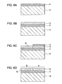
- Figs. 6A to 6D are diagrams illustrating a process for preparing a sample for evaluation by transmission electron microscopy (TEM).
- TEM transmission electron microscopy
- Figs. 7A to 7C are photographs of cross-sectional TEM images and a selected-area diffraction image.
- Figs. 8A and 8B are photographs obtained by scanning ion microscopy (SIM).
- Figs. 9A and 9B are photographs of an SIM image and an electron backscattering pattern (EBSP) image.
- EBSP electron backscattering pattern
- Figs. 10A and 10B are schematic diagrams showing analysis results of an ⁇ -tantalum structure formed in an example of the present invention.
- the inventors have studied methods for forming tantalum thin films and, as a result, have succeeded in forming a tantalum thin film with higher heat resistance and stability than known tantalum thin films. According to analysis, the tantalum thin film was determined to be ⁇ -tantalum.
- a tantalum film formed on a SiO 2 substrate has a ⁇ -tantalum crystal structure.
- heat treatment at high temperature namely, 700°C
- the inventors have achieved a method for forming an ⁇ -tantalum thin film without such heat treatment.
- the tantalum thin film was determined to have a unique structure with a periodic pattern in a plane. To date, there has been no report of such a crystal form as far as the inventors know; this is a unique crystal form first discovered by the inventors.
- Figs. 2A to 2D illustrate an example of a method for forming an ⁇ -tantalum film having the unique periodic structure.
- a silicon oxide film 11 is formed on a silicon substrate 10 by vapor deposition or thermal oxidation (in Fig. 2A).
- a ⁇ -tantalum film 12 is formed on the silicon oxide film 11 by, for example, vapor deposition (in Fig. 2B).
- a TiW film 13 is then formed (in Fig. 2C). Subsequently, the TiW film 13 is removed by etching (in Figs. 2C and 2D).
- the silicon oxide film 11 can be replaced with another substrate material on which a ⁇ -tantalum film is formed.
- a ⁇ -tantalum film examples include silicon, beryllium oxide, and aluminum oxide (e.g., Al 2 O 3 ).
- the tantalum film thus formed has a ⁇ -tantalum structure when deposited on the silicon substrate 10.
- the ⁇ -tantalum structure is transformed to an ⁇ -tantalum structure after the TiW film 13 is deposited and then removed. This allows phase transition from a ⁇ -tantalum structure to an ⁇ -tantalum structure without a heat treatment as used in the related art.
- Fig. 1 is a schematic diagram of a periodic orientation distribution structure of a metal film according to an embodiment of the present invention.
- the crystal planes of the metal film include the (001) plane, the (101) plane, and the (111) plane in terms of Miller indices.
- Fig. 3 is a diagram for illustrating that the metal film shown in Fig. 1 has a periodic pattern of crystal orientation.
- the structural unit of the periodic pattern can be considered to be a hexagon having three (001) planes and three (111) planes at its vertices.
- unit vectors A and B indicate the periodicity of the orientation distribution.
- Fig. 4 is an enlarged view of the hexagonal unit shown in Fig. 3, where individual lattice planes are illustrated with cubes representing space lattices.
- the metal film according to this embodiment has such an orientation distribution that the crystal orientation thereof is gradually rotated about a particular crystal-axis direction 15.
- the (001) plane changes to the (112) plane and then to the (111) plane with respect to the particular crystal-axis direction 15.
- the (111) plane in turn changes to the (101) plane and then back to the (111) plane.
- ⁇ 100 ⁇ planes include the (001) plane
- ⁇ 110 ⁇ planes include the (101) plane
- ⁇ 111 ⁇ planes include the (111) plane.
- the structural unit defined by the planes of the particular Miller indices is repeated in a plane.
- the crystal orientation represented by the particular Miller indices is gradually rotated about the particular crystal-axis direction 15.
- Each region having the periodic structure in a plane extends over a length of at least 10 ⁇ m, a length of at least 20 ⁇ m, or a length of at least 30 ⁇ m.
- adjacent crystal grains of an unoriented polycrystalline film can have a particular orientation relationship, they cannot have an in-plane periodic orientation relationship over a length of at least 10 ⁇ m, a length of at least 20 ⁇ m, or a length of at least 30 ⁇ m as obtained in the present invention.
- an unoriented polycrystalline film ever known has random crystal orientation in a plane. Additionally, even an oriented polycrystalline film cannot have an in-plane periodic orientation relationship over a length of several tens of micrometers.
- the metal film according to this embodiment has a unique structure in comparison with known polycrystalline films.
- Fig. 1, used in the above description, is merely illustrative of the crystal structure; actually, a deformed structure is observed, as shown in examples below.
- One of known stress relaxation mechanisms is cooperative grain boundary sliding, which is a mechanism describing large plastic deformation due to "sliding" of adjacent crystal grains at the boundaries thereof ( H. MUTO, M. SAKAI, Acta Mater. 48(2000)4161 ).
- the above stress relaxation mechanism is developed by a large stress being applied to the tantalum film by the TiW film formed thereon.
- This mechanism will transform a ⁇ -tantalum film, a metastable structure, to an ⁇ -tantalum film having a regular orientation distribution, a more stable, stress-relaxed structure.
- Other metal films in which such a regular orientation distribution occurs include films of metals with a cubic crystal structure, for example, a tungsten film, a chromium film, and a molybdenum film.
- the present invention is directed to regular orientation distribution films formed by the stress relaxation mechanism called cooperative grain boundary sliding.
- Example 1 a method for preparing a sample of a tantalum film and analysis results thereof will be described.
- Figs. 6A to 6D illustrate a process for preparing an evaluation sample.
- a silicon oxide film 11 with a thickness of about 1 ⁇ m was formed on a silicon substrate 10 by thermal oxidation.
- a tantalum film 12 with a thickness of 200 nm was formed by DC magnetron sputtering using tantalum as a target at a power output of 3 kW, a deposition pressure of 1.1 Pa, and an argon flow rate of 80 cm 3 /min.
- the TiW film 13 was removed by being dipped in a 30% hydrogen peroxide etchant heated to 45°C for five minutes.
- Figs. 7A to 7C are cross-sectional transmission electron microscopy (TEM) observation images and a selected-area electron diffraction image of the evaluation sample.
- TEM transmission electron microscopy
- the film structure of a region B where the TiW film 13 was not formed was determined to be ⁇ -tantalum (see Fig. 7C).
- the region A of the sample under measurement was irradiated with an ion beam using a focused ion beam (FIB) system, and secondary electrons emitted from the surface of the sample were detected to obtain a scanning ion microscopy (SIM) image.
- SIM scanning ion microscopy
- Figs. 8A and 8B are the SIM images obtained before and after the removal of the surface oxide film, respectively.
- the depth of penetration of irradiation ions depends on lattice planar density, which varies for different plane orientations of crystal grains (channeling effect). This results in variations in the yield of the secondary electrons, so that an image with contrast is developed. That is, the channeling contrast reveals the state of crystal orientation.
- a pattern of hexagons having vertices linked with black bands is found over the entire image. This pattern is continuously distributed in a plane. This image contrast shows that predetermined units are periodically distributed in a plane.
- An EBSP image is composed of intersecting Kikuchi bands.
- the width and intensity of the Kikuchi bands depend on crystal structure, typically lattice constant.
- the angles at which the Kikuchi bands intersect and the positions where they are developed are uniquely determined by crystal orientation.
- the crystal orientation of a sample can be identified by comparing the graphical features of an EBSP image obtained from the sample with simulation patterns of known crystal systems.
- Fig. 9A shows an SIM image of a certain ⁇ -tantalum region
- Fig. 9B shows a gradation display of orientation determined from an EBSP image of the region.
- the channeling contrast with the regular pattern observed in Fig. 8B was a reflection of the crystal orientation of ⁇ -tantalum.
- the black areas of the channeling contrast were determined to be the (001) plane, the (101) plane, and the (111) plane.
- Fig. 10A schematically illustrates the results of the EBSP image
- Fig. 10B schematically illustrates the change of crystal orientation from the (001) plane to the (111) plane.
- the metal film of this example was a high-quality thin film because no clear grain boundaries were seen in the EBSP results, at least under the condition of the present EBSP resolution.
- Example 2 A sample of Example 2 was prepared by forming a tantalum film on a silicon oxide film formed on a silicon substrate in the same manner as in Example 1, forming a TiW film on the tantalum film, and removing the TiW film therefrom by etching. Also, a sample of Comparative Example was prepared by forming a tantalum film on a silicon oxide film formed on a silicon substrate in the same manner as in Example 1.
- Table 1 shows the results of experiments for heat resistance, oxidation resistance, mechanical strength, and electrical conductivity.
- the grades of these properties are represented by the symbols A, B, and C in descending order of grade.
Landscapes
- Chemical & Material Sciences (AREA)
- Engineering & Computer Science (AREA)
- Materials Engineering (AREA)
- Metallurgy (AREA)
- Organic Chemistry (AREA)
- Mechanical Engineering (AREA)
- Chemical Kinetics & Catalysis (AREA)
- Crystallography & Structural Chemistry (AREA)
- Physical Vapour Deposition (AREA)
- Internal Circuitry In Semiconductor Integrated Circuit Devices (AREA)
- Crystals, And After-Treatments Of Crystals (AREA)
- Laminated Bodies (AREA)
- Chemical Vapour Deposition (AREA)
- Formation Of Insulating Films (AREA)
Abstract
Description
- The present invention relates to crystalline metal films.
- A variety of thin-film formation techniques, including chemical, physical, and combined techniques, have been used in a wide range of industrial fields such as semiconductor materials and magnetic materials.
- Thin films can be generally divided into polycrystalline thin films, single-crystal thin films, and amorphous thin films. The most commonly formed thin films of these are polycrystalline thin films, which can be oriented or unoriented, depending on, for example, deposition conditions. An unoriented polycrystalline thin film includes crystal grains randomly oriented so that the orientations thereof are evenly distributed in all directions. An oriented polycrystalline thin film, on the other hand, has the tendency that a particular crystal axis is preferentially aligned in a particular direction.
- Crystal structures of thin films can vary depending on, for example, the type of substrate on which the films are formed and temperature conditions. Accordingly, thin films are formed under various conditions selected according to target physical properties.
- According to R. Hoogeveen, M. Moske, et al., Thin Solid Films 275(1996)203-206, for example, a tetragonal crystal system of tantalum, namely, β-tantalum, is formed if tantalum is deposited on a substrate such as a SiO2 substrate or a BeO substrate, and a cubic crystal system of tantalum, namely, α-tantalum, is formed if tantalum is deposited on an aluminum substrate. According to this document, additionally, heat treatment up to 700°C is required for substantially complete phase transition from β-tantalum to α-tantalum.
- The present invention provides a metal film having better physical properties than known metal films.
- The present invention in its aspect provides a metal film as specified in
claims 1 to 5. - The metal film according to the present invention has a regular orientation distribution that is not found in known polycrystalline thin films and can provide better physical properties than known metal thin films.
- Further features of the present invention will become apparent from the following description of exemplary embodiments with reference to the attached drawings.
- Fig. 1 is a schematic diagram of the present invention.
- Figs. 2A to 2D are diagrams illustrating a process for forming an α-tantalum film according to an embodiment of the present invention.
- Fig. 3 is a schematic diagram of a periodic structure in the present invention.
- Fig. 4 is a schematic diagram illustrating changes of crystal orientation in the present invention.
- Fig. 5 is a diagram for illustrating a mechanism by which the crystal structure according to the present invention is formed.
- Figs. 6A to 6D are diagrams illustrating a process for preparing a sample for evaluation by transmission electron microscopy (TEM).
- Figs. 7A to 7C are photographs of cross-sectional TEM images and a selected-area diffraction image.
- Figs. 8A and 8B are photographs obtained by scanning ion microscopy (SIM).
- Figs. 9A and 9B are photographs of an SIM image and an electron backscattering pattern (EBSP) image.
- Figs. 10A and 10B are schematic diagrams showing analysis results of an α-tantalum structure formed in an example of the present invention.
- The inventors have studied methods for forming tantalum thin films and, as a result, have succeeded in forming a tantalum thin film with higher heat resistance and stability than known tantalum thin films. According to analysis, the tantalum thin film was determined to be α-tantalum.
- A tantalum film formed on a SiO2 substrate has a β-tantalum crystal structure. Conventionally, heat treatment at high temperature, namely, 700°C, is required to transform the β-tantalum crystal structure to α-tantalum. The inventors have achieved a method for forming an α-tantalum thin film without such heat treatment.
- According to further analysis, the tantalum thin film was determined to have a unique structure with a periodic pattern in a plane. To date, there has been no report of such a crystal form as far as the inventors know; this is a unique crystal form first discovered by the inventors.
- A detailed description will now be given of the unique periodic crystal structure according to the present invention, and of a method for forming such a tantalum thin film which triggered the discovery of the crystal structure.
- Figs. 2A to 2D illustrate an example of a method for forming an α-tantalum film having the unique periodic structure.
- A
silicon oxide film 11 is formed on asilicon substrate 10 by vapor deposition or thermal oxidation (in Fig. 2A). A β-tantalum film 12 is formed on thesilicon oxide film 11 by, for example, vapor deposition (in Fig. 2B). A TiWfilm 13 is then formed (in Fig. 2C). Subsequently, the TiWfilm 13 is removed by etching (in Figs. 2C and 2D). - The
silicon oxide film 11 can be replaced with another substrate material on which a β-tantalum film is formed. Examples of such a material include silicon, beryllium oxide, and aluminum oxide (e.g., Al2O3). - The tantalum film thus formed has a β-tantalum structure when deposited on the
silicon substrate 10. The β-tantalum structure is transformed to an α-tantalum structure after theTiW film 13 is deposited and then removed. This allows phase transition from a β-tantalum structure to an α-tantalum structure without a heat treatment as used in the related art. - Fig. 1 is a schematic diagram of a periodic orientation distribution structure of a metal film according to an embodiment of the present invention. In Fig. 1, the crystal planes of the metal film include the (001) plane, the (101) plane, and the (111) plane in terms of Miller indices. Fig. 3 is a diagram for illustrating that the metal film shown in Fig. 1 has a periodic pattern of crystal orientation. In Fig. 3, the structural unit of the periodic pattern can be considered to be a hexagon having three (001) planes and three (111) planes at its vertices. In Fig. 3, unit vectors A and B indicate the periodicity of the orientation distribution.
- Fig. 4 is an enlarged view of the hexagonal unit shown in Fig. 3, where individual lattice planes are illustrated with cubes representing space lattices. In Fig. 4, the metal film according to this embodiment has such an orientation distribution that the crystal orientation thereof is gradually rotated about a particular crystal-
axis direction 15. The (001) plane changes to the (112) plane and then to the (111) plane with respect to the particular crystal-axis direction 15. The (111) plane in turn changes to the (101) plane and then back to the (111) plane. In a cubic crystal system, {100} planes include the (001) plane, {110} planes include the (101) plane, and {111} planes include the (111) plane. - In the periodic structure of the metal film according to this embodiment, as described above, the structural unit defined by the planes of the particular Miller indices is repeated in a plane. In addition, the crystal orientation represented by the particular Miller indices is gradually rotated about the particular crystal-
axis direction 15. Each region having the periodic structure in a plane extends over a length of at least 10 µm, a length of at least 20 µm, or a length of at least 30 µm. - Although in general adjacent crystal grains of an unoriented polycrystalline film can have a particular orientation relationship, they cannot have an in-plane periodic orientation relationship over a length of at least 10 µm, a length of at least 20 µm, or a length of at least 30 µm as obtained in the present invention. Unlike the metal film according to this embodiment, an unoriented polycrystalline film ever known has random crystal orientation in a plane. Additionally, even an oriented polycrystalline film cannot have an in-plane periodic orientation relationship over a length of several tens of micrometers.
- As described above, the metal film according to this embodiment has a unique structure in comparison with known polycrystalline films. Fig. 1, used in the above description, is merely illustrative of the crystal structure; actually, a deformed structure is observed, as shown in examples below.
- The mechanism by which the regular orientation distribution film according to this embodiment is formed has not yet been clearly understood, although at present the inventors presume the mechanism to be as follows.
- Stress on a thin film is affected by a lower interface with an underlying substrate and, if in contact with an overlying solid, is also affected by an upper interface with the solid. Hence, a change in such a direction as to relax the stress will be facilitated if the lower or upper interface develops any deformation or structural transformation mechanism capable of relaxing the stress in the thin film.
- One of known stress relaxation mechanisms is cooperative grain boundary sliding, which is a mechanism describing large plastic deformation due to "sliding" of adjacent crystal grains at the boundaries thereof (H. MUTO, M. SAKAI, Acta Mater. 48(2000)4161).
- If a single-crystal region with the (111) plane in a cubic crystal system is taken as a starting point, as shown in Fig. 5, three equivalent <110> directions are found every about 120° in the (111) plane (six <110> directions are found if reverse directions are distinguished). Hence, the orientation distribution with the regular pattern having the hexagonal fundamental unit shown in Fig. 3 will be formed if crystal grains are sequentially formed such that the crystal orientation thereof is rotated about the three <110> directions every predetermined angle.
- In this embodiment, the above stress relaxation mechanism is developed by a large stress being applied to the tantalum film by the TiW film formed thereon. This mechanism will transform a β-tantalum film, a metastable structure, to an α-tantalum film having a regular orientation distribution, a more stable, stress-relaxed structure. Other metal films in which such a regular orientation distribution occurs include films of metals with a cubic crystal structure, for example, a tungsten film, a chromium film, and a molybdenum film.
- As discussed above, the present invention is directed to regular orientation distribution films formed by the stress relaxation mechanism called cooperative grain boundary sliding.
- In Example 1, a method for preparing a sample of a tantalum film and analysis results thereof will be described.
- Figs. 6A to 6D illustrate a process for preparing an evaluation sample.
- Referring to Fig. 6A, a
silicon oxide film 11 with a thickness of about 1 µm was formed on asilicon substrate 10 by thermal oxidation. Referring to Fig. 6B, atantalum film 12 with a thickness of 200 nm was formed by DC magnetron sputtering using tantalum as a target at a power output of 3 kW, a deposition pressure of 1.1 Pa, and an argon flow rate of 80 cm3/min. - Referring to Fig. 6C, a
TiW film 13 with a thickness of 200 nm was selectively formed on thetantalum film 12 by DC magnetron sputtering with a metal mask partially covering thetantalum film 12 using a TiW alloy (Ti:W = 1:9) as a target at a power output of 2.7 kW, a deposition pressure of 1.1 Pa, an argon flow rate of 80 cm3/min, a substrate temperature of 150°C, and a deposition rate of 11 nm/min. - Referring to Fig. 6D, the
TiW film 13 was removed by being dipped in a 30% hydrogen peroxide etchant heated to 45°C for five minutes. - Figs. 7A to 7C are cross-sectional transmission electron microscopy (TEM) observation images and a selected-area electron diffraction image of the evaluation sample.
- The cross-sectional TEM observation (see Fig. 7A) and the selected-area electron diffraction (see Fig. 7B) proved that the film structure of a region A (see Fig. 6D) where the
TiW film 13 was selectively formed was transformed to α-tantalum. - On the other hand, the film structure of a region B where the
TiW film 13 was not formed was determined to be β-tantalum (see Fig. 7C). - Next, the region A of the sample under measurement was irradiated with an ion beam using a focused ion beam (FIB) system, and secondary electrons emitted from the surface of the sample were detected to obtain a scanning ion microscopy (SIM) image. Another SIM image was obtained after a surface oxide film was removed with an ion beam.
- Figs. 8A and 8B are the SIM images obtained before and after the removal of the surface oxide film, respectively. In the FIB system, the depth of penetration of irradiation ions depends on lattice planar density, which varies for different plane orientations of crystal grains (channeling effect). This results in variations in the yield of the secondary electrons, so that an image with contrast is developed. That is, the channeling contrast reveals the state of crystal orientation.
- In Fig. 8B, a pattern of hexagons having vertices linked with black bands is found over the entire image. This pattern is continuously distributed in a plane. This image contrast shows that predetermined units are periodically distributed in a plane.
- Next, the crystal orientation, which could not be identified only with the SIM image, was identified in terms of Miller indices using an electron backscattering pattern (EBSP).
- An EBSP image is composed of intersecting Kikuchi bands. The width and intensity of the Kikuchi bands depend on crystal structure, typically lattice constant. In addition, the angles at which the Kikuchi bands intersect and the positions where they are developed are uniquely determined by crystal orientation. Hence, the crystal orientation of a sample can be identified by comparing the graphical features of an EBSP image obtained from the sample with simulation patterns of known crystal systems.
- Fig. 9A shows an SIM image of a certain α-tantalum region, and Fig. 9B shows a gradation display of orientation determined from an EBSP image of the region.
- These results demonstrated that the channeling contrast with the regular pattern observed in Fig. 8B was a reflection of the crystal orientation of α-tantalum. In addition, the black areas of the channeling contrast were determined to be the (001) plane, the (101) plane, and the (111) plane.
- Fig. 10A schematically illustrates the results of the EBSP image, and Fig. 10B schematically illustrates the change of crystal orientation from the (001) plane to the (111) plane. These figures show that the tantalum film of this example had such an in-plane distribution that the crystal orientation thereof was gradually rotated about a particular crystal axis.
- To date, there has been no report of such a film structure as far as the inventors know; this is a unique crystal form first discovered by the inventors. In addition, the metal film of this example was a high-quality thin film because no clear grain boundaries were seen in the EBSP results, at least under the condition of the present EBSP resolution.
- A sample of Example 2 was prepared by forming a tantalum film on a silicon oxide film formed on a silicon substrate in the same manner as in Example 1, forming a TiW film on the tantalum film, and removing the TiW film therefrom by etching. Also, a sample of Comparative Example was prepared by forming a tantalum film on a silicon oxide film formed on a silicon substrate in the same manner as in Example 1.
- Table 1 shows the results of experiments for heat resistance, oxidation resistance, mechanical strength, and electrical conductivity. The grades of these properties are represented by the symbols A, B, and C in descending order of grade. These results show that the regular orientation distribution α-tantalum film had higher film quality than the β-tantalum film.
- It seems that an α-tantalum film with no regular orientation distribution has lower film quality than one with regular orientation distribution because of lower flatness and the presence of clear grain boundaries.
Table 1 Heat resistance Oxidation resistance Mechanical strength Electrical conductivity Example 2 (regular orientation distribution α-tantalum film) A A A A Comparative Example (β-tantalum film) B C A C - While the present invention has been described with reference to exemplary embodiments, it is to be understood that the invention is not limited to the disclosed exemplary embodiments. The scope of the following claims is to be accorded the broadest interpretation so as to encompass all modifications, equivalent structures and functions.
Claims (5)
- A metal film having a cubic crystal structure, the metal film having a periodic pattern of crystal orientation in a plane, the crystal orientation being gradually rotated about a particular crystal-axis direction (15) such that a {100} plane, a {110} plane, and a {111} plane appear.
- The metal film according to Claim 1, wherein each region having the periodic pattern of crystal orientation in a plane extends over a length of 10 µm or more.
- The metal film according to Claim 1, wherein the metal film is a tantalum film, a tungsten film, a chromium film, or a molybdenum film.
- The metal film according to Claim 1, wherein the metal film is formed on a substrate (11).
- The metal film according to Claim 4, wherein the substrate (11) comprises silicon, silicon oxide, beryllium oxide, or aluminum oxide.
Applications Claiming Priority (2)
| Application Number | Priority Date | Filing Date | Title |
|---|---|---|---|
| JP2006219168 | 2006-08-11 | ||
| JP2007165231A JP4290211B2 (en) | 2006-08-11 | 2007-06-22 | Crystalline metal film |
Publications (3)
| Publication Number | Publication Date |
|---|---|
| EP1918428A2 true EP1918428A2 (en) | 2008-05-07 |
| EP1918428A3 EP1918428A3 (en) | 2009-07-01 |
| EP1918428B1 EP1918428B1 (en) | 2013-10-16 |
Family
ID=38924376
Family Applications (1)
| Application Number | Title | Priority Date | Filing Date |
|---|---|---|---|
| EP07015625.2A Not-in-force EP1918428B1 (en) | 2006-08-11 | 2007-08-08 | Crystalline tantalum film and method of forming it |
Country Status (4)
| Country | Link |
|---|---|
| US (1) | US7553381B2 (en) |
| EP (1) | EP1918428B1 (en) |
| JP (1) | JP4290211B2 (en) |
| KR (1) | KR101009964B1 (en) |
Families Citing this family (2)
| Publication number | Priority date | Publication date | Assignee | Title |
|---|---|---|---|---|
| JP6808560B2 (en) * | 2017-04-03 | 2021-01-06 | 株式会社豊田中央研究所 | Sliding system |
| CN118854223B (en) * | 2024-09-24 | 2025-01-03 | 中国科学技术大学 | Body-centered cubic tantalum film and preparation method and application thereof |
Family Cites Families (6)
| Publication number | Priority date | Publication date | Assignee | Title |
|---|---|---|---|---|
| US4192695A (en) * | 1976-04-16 | 1980-03-11 | Shalom Mahalla | Metal crystals and process |
| JPH1148488A (en) | 1997-08-05 | 1999-02-23 | Canon Inc | Method for manufacturing liquid discharge head and liquid discharge head |
| US6374482B1 (en) | 1997-08-05 | 2002-04-23 | Canon Kabushiki Kaisha | Method of manufacturing a liquid discharge head |
| US6955835B2 (en) | 2003-04-30 | 2005-10-18 | Hewlett-Packard Development Company, L.P. | Method for forming compressive alpha-tantalum on substrates and devices including the same |
| JP4593475B2 (en) | 2003-11-06 | 2010-12-08 | Jx日鉱日石金属株式会社 | Tantalum sputtering target |
| JP2008051200A (en) * | 2006-08-24 | 2008-03-06 | Tokai Rubber Ind Ltd | Bush manufacturing method |
-
2007
- 2007-06-22 JP JP2007165231A patent/JP4290211B2/en not_active Expired - Fee Related
- 2007-08-03 KR KR1020070077976A patent/KR101009964B1/en not_active Expired - Fee Related
- 2007-08-07 US US11/834,983 patent/US7553381B2/en not_active Expired - Fee Related
- 2007-08-08 EP EP07015625.2A patent/EP1918428B1/en not_active Not-in-force
Non-Patent Citations (1)
| Title |
|---|
| R. HOOGEVEEN; M. MOSKE ET AL., THIN SOLID FILMS, vol. 275, 1996, pages 203 - 206 |
Also Published As
| Publication number | Publication date |
|---|---|
| US7553381B2 (en) | 2009-06-30 |
| EP1918428B1 (en) | 2013-10-16 |
| JP2008063216A (en) | 2008-03-21 |
| US20080038147A1 (en) | 2008-02-14 |
| JP4290211B2 (en) | 2009-07-01 |
| EP1918428A3 (en) | 2009-07-01 |
| KR20080014617A (en) | 2008-02-14 |
| KR101009964B1 (en) | 2011-01-20 |
Similar Documents
| Publication | Publication Date | Title |
|---|---|---|
| Lu et al. | Surface morphology and microstructure of pulsed DC magnetron sputtered piezoelectric AlN and AlScN thin films | |
| Tselev et al. | Interplay between ferroelastic and metal− insulator phase transitions in strained quasi-two-dimensional VO2 nanoplatelets | |
| Popović et al. | Structural, optical and electrical properties of argon implanted TiN thin films | |
| Signore et al. | Growth assessment of (002)-oriented AlN thin films on Ti bottom electrode deposited on silicon and kapton substrates | |
| Oreshkin et al. | In situ visualization of Ni–Nb bulk metallic glasses phase transition | |
| Pavlovska et al. | Surface roughening and surface melting the high temperature equilibrium shape of small Pb crystals | |
| TW202239981A (en) | Magnetic material, laminate, and method for producing laminate, thermoelectric conversion element, and magnetic sensor | |
| Yoshikawa et al. | Wafer bowing control of free-standing heteroepitaxial diamond (100) films grown on Ir (100) substrates via patterned nucleation growth | |
| Rogge et al. | On the rotational alignment of graphene domains grown on Ge (110) and Ge (111) | |
| KR20240006566A (en) | Manufacturing process of aluminum scandium nitride membrane | |
| Pofelski et al. | Domain nucleation across the metal-insulator transition of self-strained V 2 O 3 films | |
| Hoseinzadeh et al. | Tantalum/Nitrogen and n-type WO3 Semiconductor/FTO Structures as a Cathode for the Future of Nanodevices | |
| EP1918428B1 (en) | Crystalline tantalum film and method of forming it | |
| Müller et al. | Epitaxial growth of boron nitride on a Rh (1 1 1) multilayer system: Formation and fine tuning of a BN-nanomesh | |
| US20170287727A1 (en) | Metal hard mask and method of manufacturing same | |
| Schuler et al. | Comparison of DC and RF sputtered zinc oxide films with post-annealing and dry etching and effect on crystal composition | |
| Yong et al. | Cool copper template for the formation of oriented nanocrystalline α-tantalum | |
| Hanani et al. | Unlocking high capacitive energy-density in Sm-doped Pb (Mg 1/3 Nb 2/3) O 3–PbTiO 3 thin films via strain and domain engineering | |
| Siegal et al. | Improving Bi2Te3-based thermoelectric nanowire microstructure via thermal processing | |
| JP2017163127A (en) | Metal nitride film structure for thermistor and method of manufacturing the same, and thermistor sensor | |
| KR102265089B1 (en) | Graphene synthetic method for conductive property control | |
| JP4913401B2 (en) | Method for forming platinum thin film | |
| Tillmann et al. | Atomic structure of β-Tantalum nanocrystallites | |
| US20250361601A1 (en) | Method for controlling specific resistivity and stress of tungsten through pvd sputtering method | |
| Bovet et al. | Geometrical and electronic structure of Pd clusters on graphite |
Legal Events
| Date | Code | Title | Description |
|---|---|---|---|
| PUAI | Public reference made under article 153(3) epc to a published international application that has entered the european phase |
Free format text: ORIGINAL CODE: 0009012 |
|
| AK | Designated contracting states |
Kind code of ref document: A2 Designated state(s): AT BE BG CH CY CZ DE DK EE ES FI FR GB GR HU IE IS IT LI LT LU LV MC MT NL PL PT RO SE SI SK TR |
|
| AX | Request for extension of the european patent |
Extension state: AL BA HR MK RS |
|
| PUAL | Search report despatched |
Free format text: ORIGINAL CODE: 0009013 |
|
| AK | Designated contracting states |
Kind code of ref document: A3 Designated state(s): AT BE BG CH CY CZ DE DK EE ES FI FR GB GR HU IE IS IT LI LT LU LV MC MT NL PL PT RO SE SI SK TR |
|
| AX | Request for extension of the european patent |
Extension state: AL BA HR MK RS |
|
| RIC1 | Information provided on ipc code assigned before grant |
Ipc: C30B 23/02 20060101ALI20090526BHEP Ipc: C23C 14/18 20060101ALI20090526BHEP Ipc: C30B 29/02 20060101AFI20080118BHEP |
|
| 17P | Request for examination filed |
Effective date: 20100104 |
|
| AKX | Designation fees paid |
Designated state(s): DE FR GB IT |
|
| 17Q | First examination report despatched |
Effective date: 20100330 |
|
| REG | Reference to a national code |
Ref country code: DE Ref legal event code: R079 Ref document number: 602007033308 Country of ref document: DE Free format text: PREVIOUS MAIN CLASS: C30B0029020000 Ipc: C30B0023020000 |
|
| GRAP | Despatch of communication of intention to grant a patent |
Free format text: ORIGINAL CODE: EPIDOSNIGR1 |
|
| RIC1 | Information provided on ipc code assigned before grant |
Ipc: C23C 14/16 20060101ALI20130207BHEP Ipc: C23C 14/02 20060101ALI20130207BHEP Ipc: C30B 29/02 20060101ALI20130207BHEP Ipc: C30B 23/02 20060101AFI20130207BHEP Ipc: C23C 14/58 20060101ALI20130207BHEP |
|
| GRAS | Grant fee paid |
Free format text: ORIGINAL CODE: EPIDOSNIGR3 |
|
| GRAA | (expected) grant |
Free format text: ORIGINAL CODE: 0009210 |
|
| AK | Designated contracting states |
Kind code of ref document: B1 Designated state(s): DE FR GB IT |
|
| REG | Reference to a national code |
Ref country code: GB Ref legal event code: FG4D |
|
| REG | Reference to a national code |
Ref country code: DE Ref legal event code: R096 Ref document number: 602007033308 Country of ref document: DE Effective date: 20131212 |
|
| REG | Reference to a national code |
Ref country code: DE Ref legal event code: R097 Ref document number: 602007033308 Country of ref document: DE |
|
| PLBE | No opposition filed within time limit |
Free format text: ORIGINAL CODE: 0009261 |
|
| STAA | Information on the status of an ep patent application or granted ep patent |
Free format text: STATUS: NO OPPOSITION FILED WITHIN TIME LIMIT |
|
| PG25 | Lapsed in a contracting state [announced via postgrant information from national office to epo] |
Ref country code: IT Free format text: LAPSE BECAUSE OF FAILURE TO SUBMIT A TRANSLATION OF THE DESCRIPTION OR TO PAY THE FEE WITHIN THE PRESCRIBED TIME-LIMIT Effective date: 20131016 |
|
| 26N | No opposition filed |
Effective date: 20140717 |
|
| REG | Reference to a national code |
Ref country code: DE Ref legal event code: R097 Ref document number: 602007033308 Country of ref document: DE Effective date: 20140717 |
|
| REG | Reference to a national code |
Ref country code: FR Ref legal event code: PLFP Year of fee payment: 9 |
|
| PGFP | Annual fee paid to national office [announced via postgrant information from national office to epo] |
Ref country code: GB Payment date: 20150826 Year of fee payment: 9 Ref country code: DE Payment date: 20150831 Year of fee payment: 9 |
|
| PGFP | Annual fee paid to national office [announced via postgrant information from national office to epo] |
Ref country code: FR Payment date: 20150826 Year of fee payment: 9 |
|
| REG | Reference to a national code |
Ref country code: DE Ref legal event code: R119 Ref document number: 602007033308 Country of ref document: DE |
|
| GBPC | Gb: european patent ceased through non-payment of renewal fee |
Effective date: 20160808 |
|
| REG | Reference to a national code |
Ref country code: FR Ref legal event code: ST Effective date: 20170428 |
|
| PG25 | Lapsed in a contracting state [announced via postgrant information from national office to epo] |
Ref country code: DE Free format text: LAPSE BECAUSE OF NON-PAYMENT OF DUE FEES Effective date: 20170301 Ref country code: GB Free format text: LAPSE BECAUSE OF NON-PAYMENT OF DUE FEES Effective date: 20160808 Ref country code: FR Free format text: LAPSE BECAUSE OF NON-PAYMENT OF DUE FEES Effective date: 20160831 |